EP3742257B1 - System und verfahren zur leistungsmodusverwaltung für einen prozessor - Google Patents
System und verfahren zur leistungsmodusverwaltung für einen prozessor Download PDFInfo
- Publication number
- EP3742257B1 EP3742257B1 EP19305638.9A EP19305638A EP3742257B1 EP 3742257 B1 EP3742257 B1 EP 3742257B1 EP 19305638 A EP19305638 A EP 19305638A EP 3742257 B1 EP3742257 B1 EP 3742257B1
- Authority
- EP
- European Patent Office
- Prior art keywords
- power
- standby
- mode
- low power
- processor
- Prior art date
- Legal status (The legal status is an assumption and is not a legal conclusion. Google has not performed a legal analysis and makes no representation as to the accuracy of the status listed.)
- Active
Links
Images


Classifications
-
- G—PHYSICS
- G06—COMPUTING OR CALCULATING; COUNTING
- G06F—ELECTRIC DIGITAL DATA PROCESSING
- G06F1/00—Details not covered by groups G06F3/00 - G06F13/00 and G06F21/00
- G06F1/26—Power supply means, e.g. regulation thereof
- G06F1/32—Means for saving power
- G06F1/3203—Power management, i.e. event-based initiation of a power-saving mode
- G06F1/3206—Monitoring of events, devices or parameters that trigger a change in power modality
-
- G—PHYSICS
- G06—COMPUTING OR CALCULATING; COUNTING
- G06F—ELECTRIC DIGITAL DATA PROCESSING
- G06F1/00—Details not covered by groups G06F3/00 - G06F13/00 and G06F21/00
- G06F1/26—Power supply means, e.g. regulation thereof
-
- G—PHYSICS
- G06—COMPUTING OR CALCULATING; COUNTING
- G06F—ELECTRIC DIGITAL DATA PROCESSING
- G06F1/00—Details not covered by groups G06F3/00 - G06F13/00 and G06F21/00
- G06F1/26—Power supply means, e.g. regulation thereof
- G06F1/32—Means for saving power
- G06F1/3203—Power management, i.e. event-based initiation of a power-saving mode
- G06F1/3234—Power saving characterised by the action undertaken
- G06F1/3287—Power saving characterised by the action undertaken by switching off individual functional units in the computer system
-
- G—PHYSICS
- G06—COMPUTING OR CALCULATING; COUNTING
- G06F—ELECTRIC DIGITAL DATA PROCESSING
- G06F11/00—Error detection; Error correction; Monitoring
- G06F11/07—Responding to the occurrence of a fault, e.g. fault tolerance
- G06F11/0703—Error or fault processing not based on redundancy, i.e. by taking additional measures to deal with the error or fault not making use of redundancy in operation, in hardware, or in data representation
- G06F11/0751—Error or fault detection not based on redundancy
- G06F11/0754—Error or fault detection not based on redundancy by exceeding limits
- G06F11/0757—Error or fault detection not based on redundancy by exceeding limits by exceeding a time limit, i.e. time-out, e.g. watchdogs
-
- G—PHYSICS
- G06—COMPUTING OR CALCULATING; COUNTING
- G06F—ELECTRIC DIGITAL DATA PROCESSING
- G06F11/00—Error detection; Error correction; Monitoring
- G06F11/07—Responding to the occurrence of a fault, e.g. fault tolerance
- G06F11/0796—Safety measures, i.e. ensuring safe condition in the event of error, e.g. for controlling element
-
- G—PHYSICS
- G06—COMPUTING OR CALCULATING; COUNTING
- G06F—ELECTRIC DIGITAL DATA PROCESSING
- G06F11/00—Error detection; Error correction; Monitoring
- G06F11/22—Detection or location of defective computer hardware by testing during standby operation or during idle time, e.g. start-up testing
- G06F11/2284—Detection or location of defective computer hardware by testing during standby operation or during idle time, e.g. start-up testing by power-on test, e.g. power-on self test [POST]
Definitions
- the present invention relates in general to processor power mode management, and more particularly to a system and method of ensuring that power mode transitions take place in a robust and secure manner to reduce potential of failure.
- a processor or processing unit such as a microprocessor, microcontroller, system on chip or any other processing configuration, may be used to process any type of data or information to control certain parameters, functions or operations associated with a particular application.
- Automotive applications may include, for example, gateways (e.g., in-vehicle networking and telematics), adaptive driver assistance systems (ADAS), infotainment (audio and/or video entertainment, information, navigation, hands-free control, etc.), clusters (digital instrumentation, heads-up display, etc.), vehicle to everything (V2X) (e.g., communication between a vehicle and external entities, traffic sign recognition, etc.), radar, vision (e.g., cameras, proximity sensors, collision avoidance, blind spot monitoring, etc.).
- Industrial applications may include, for example, industrial tablets or laptops and the like, internet protocol television (IPTV), industrial control, medical monitoring, home automation and/or alarm systems, etc.
- IPTV internet protocol television
- a processor may have a low power mode, such as a standby mode or the like, to minimize power consumption during periods of inactivity in which all but a minimum amount of logic is powered down.
- An external Power Management IC PMIC
- PMIC may be used to provide supply voltage to the processor, and may further be used to control the power mode of the processor including transitioning between normal and low power modes.
- any miscommunication between the processor and the PMIC could lead to power being removed at an incorrect time, causing the processor and any corresponding peripherals to be unexpectedly powered down.
- safety is a concern including safety critical applications, the consequences of unexpected power down could be inconvenient or even dangerous in the event the system is unable to transition to a safe state.
- US 2016/360106 A1 discloses an electronic circuit capable of entering and exiting a standby mode of operation, wherein a pre-standby mode is disclosed in order to allow a quick recovery in the active mode, if a turn on signal is applied during the pre-standby mode.
- US 2013/086283 A1 discloses an electronic device capable of transitioning between a standard mode of operation and a high speed mode of operation. Furthermore, D3 discloses the use of a safe standard mode of operation when transitioning from the standard mode to the high speed mode of operation as well as a safe high speed mode of operation when transitioning from the high speed mode to the standard mode of operation.
- US 2014/149769 A1 discloses an electronic device capable of transitioning between different power consumption states using a safety supervisor unit, which provides a range of power supply voltages in which the operation of a given frequency is considered not to cause an error due to a critical path during operation.
- the inventors have recognized that it is advantageous to provide a robust and safe method to transition between a normal mode of operation and a low power mode of operation between a processor and a power management IC (PMIC) while also ensuring that communications across the interface are accurate.
- the normal mode means that the system is fully powered to perform the functions and operations for which the system was designed.
- the low power mode represents any reduced power mode (e.g., reduced power mode, sleep mode, standby mode, etc.) that reduces quiescent current in order to reduce overall power consumption.
- a system and method of power mode management as described herein provides dedicated interactions to ensure that transitions between the different modes of operation are safe and robust, such as ensuring that the processor does not unexpectedly transition to its low power mode when system critical functions are being performed.
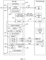
- FIG. 1 is a simplified block diagram of a processing system 102 implemented according to one embodiment of the present disclosure.
- the processing system 102 may be implemented in a discrete manner or may be integrated onto a single module, such as a system on chip (SoC) or the like.
- the processing system 102 includes a power management IC (PMIC) 104, a processor 106, peripheral system 108, and a memory & storage module 110.
- PMIC power management IC
- the PMIC 104 cooperates with the processor 106 to ensure that power mode transitions of the processor 106 (and transitions of any other devices powered by the PMIC 104) take place in a robust and secure manner to reduce potential of failure as further described herein.
- the processor 106 may include any type of processing device or system, such as programmable integrated circuit, a microprocessor, a microcontroller or MCU, a central processing unit (CPU), an application processor, etc., and may include multiple processing devices.
- the memory & storage module 110 may include one or more of any type of memory or storage devices or any combination thereof, including, for example, random access memory (RAM), dynamic RAM (DRAM), synchronous DRAM (SDRAM), low power double data rate (DDR) (LPDDR4), non-volatile memory such as serial peripheral interface (SPI) Flash memory 190, NVRAM, Flash memory, solid state drive/s (SSDs), hard disk drive/s, optical drives, or any other suitable form of internal or external storage.
- RAM random access memory
- DRAM dynamic RAM
- SDRAM synchronous DRAM
- DDR low power double data rate
- SPI serial peripheral interface
- Flash memory 190
- NVRAM non-volatile memory
- Flash memory solid state drive/s
- SSDs solid state drive/
- the processing system 102 may be used to implement or may be part of an automotive application or an industrial application or the like in which safety and robustness are of concern.
- the peripheral system 108 may be used to interface sensors, communication devices, detectors, display devices, keyboards, controllers, mice, etc., to enable the processor 106 to process any type of data or information to control certain parameters, functions or operations associated with the particular application.
- the processor 106 includes a low power mode to reduce power consumption in which only a minimal amount of logic and circuitry remains powered sufficient to reawaken the processing system 102 to resume normal operations.
- the PMIC 104 controls the supply voltage provided to the PROC 106 (and any other peripherals) and further facilitates transitioning the processor 106 between its normal and low power modes as further described herein.
- the PMIC 104 also has a low power mode referred to herein as a "standby" mode in which it maintains a very low yet sufficient level of operation to detect a request by the processor 106 to reawaken the system.
- FIG. 2 is a more detailed block diagram of the PMIC 104 interfacing the processor 106 for controlling power mode transitions according to one embodiment of the present disclosure.
- the PMIC 104 is divided into two different modules for two different domains, including a power management processing module 202 and a safety processing module 204.
- the power management processing module 202 includes a power management (PM) control circuit 203 that generally controls operation of the power management processing module 202.
- the power management processing module 202 includes a power converter 206 including at least one switchable regulator that converts an input voltage VIN into at least one supply voltage (SV) provided on at least one voltage rail 207 sufficient to operate the processor 106.
- the input voltage VIN may be provided by any type of power source depending upon the particular application.
- VIN may be provided by 12 Volt (V), 24V, or 48V battery or the like.
- Industrial applications may be powered by a battery or by a converter or inverter or the like providing VIN converted from an alternating current (AC) source voltage or the like.
- SV may be a single voltage or may include multiple voltages, such as, for example, 0.8V, 1.1V, 1.8V, 3.3V, 5V, etc.
- SV is referred to herein as a single source voltage in which it is understood that SV may include multiple different voltage levels.
- the power converter 206 may include at least one non-switched regulator that remains on to power circuitry of the PMIC 104 during its standby mode.
- the power management processing module 202 also includes a standby timing window (STW) counter 208 that is programmed with a standby timing value that defines a maximum amount of time for the processing system 102 to remain in the standby mode.
- the standby timing value is configurable for different configurations.
- the power management processing module 202 includes a communication interface (COMM I/F) 210 coupled to a communication bus 211 that enables communication with the processor 106.
- the communication interface 210 and the communication bus 211 are configured as a serial communications interface, such as, for example, the inter-integrated circuit (I2C) serial communication interface configured according to the I2C protocol, although any suitable communication interface may be used, such as, for example, a serial peripheral interface (SPI) or the like.
- I2C inter-integrated circuit
- SPI serial peripheral interface
- the PMIC 104 further includes a standby exit (STBY_EXIT) pin and a standby power good (STBY_PGOOD) pin which are both monitored and controlled by the PM control circuit 203 as further described herein.
- STBY_EXIT standby exit
- STBY_PGOOD standby power good
- the STBY_EXIT pin is asserted high by the processor 106 to request exit from its low power mode by requesting that the PMIC 104 exit its standby mode. It is noted that as used throughout this disclosure, a pin or a signal is "asserted” high and “de-asserted” low or otherwise is asserted low and de-asserted high depending upon logical context.
- the state of the STBY_PGOOD pin indicates the voltage level of SV.
- the STBY_PGOOD pin may be asserted high to indicate to the processor 106 that SV is charged above a high voltage threshold level HVTH for entering the normal mode.
- the STBY_PGOOD pin may be asserted low to indicate to the processor 106 that SV is discharged below a configurable low voltage threshold level LVTH for entering its low power mode from the normal mode.
- the HVTH level is determined to indicate that the switchable regulator(s) is fully charged and SV is above a minimum level for fully powering the processor 106.
- the LVTH level is determined to verify that the switchable regulator(s) is sufficiently discharged to ensure that the powered-down portion of the processor 106 may be restarted with no residual internal biasing.
- each individual source voltage may have a different low threshold voltage level and a different high threshold voltage level.
- STBY_PGOOD indicates that each source voltage is above a corresponding one of multiple high voltage threshold levels or is below a corresponding one of multiple low voltage threshold levels.
- STBY_PGOOD may be a single pin with hysteresis function in which it starts low and transitions high only after SV > HVTH, and then transitions back low only after SV ⁇ LVTH.
- STBY_PGOOD may be implemented as two separate pins, such as PHI and PLO (not shown).
- the state of PLO indicates whether or not SV is below LVTH whereas the state of PHI indicates whether or not SV is above HVTH.
- separate power good signals or signal pairs may be provided for each SV. Operation is similar in each of these alternative embodiments in which multiple status signals may be considered in combination.
- the safety processing module 204 includes a safety control circuit 205 that generally controls operation of the safety processing module 204.
- the safety processing module 204 includes cyclic redundancy check (CRC) logic 212 interfaced with the communication interface 210 to protect the integrity of end to end communication with the processor 106.
- the safety processing module 204 includes a standby (STBY) register 214 used for a first step in a two step standby process for transitioning to the standby mode as further described herein.
- the safety processing module 204 includes a standby entry timing (SET) counter 216 that is programmed with a standby entry timing value that defines a maximum time between the first and second steps of the two step standby process as further described herein.
- SET standby entry timing
- the safety processing module 204 includes a memory circuit 217 that includes a first memory element (ME) 218 coupled to a reset pin RSTB and a second memory element 219 coupled to a fail safe pin FSOB of the PMIC 104.
- the fail safe pin FSOB is coupled to external application safe state logic (ASSL) 240 to maintain the safe state of the application, which is not further described herein.
- the safety processing module 204 includes a safety processing supply (SPS) 220 and a memory elements safety processing supply (MES PS) 222, in which the memory elements safety processing supply 222 provides power to the memory elements 218 and 219 of the memory circuit 217.
- SPS safety processing supply
- MES PS memory elements safety processing supply
- the safety processing module 204 includes a standby entry pin (FS_STBY_ENTRY) pin that is coupled to a STBY pin of the processor 106.
- the processor 106 requests entry into its low power mode by asserting its STBY pin low as further described herein, which thus asserts the FS_STBY_ENTRY pin of the PMIC 104 low.
- the safety processing module 204 includes logical built-in self-test (LBIST) circuit 224 to check the integrity of the logic of the safety processing module 204 and also includes analog built-in self-test (ABIST) circuit 226 to check the integrity of the memory circuit 217 and the states of the FSOB and RSTB pins.
- the safety processing module 204 includes an acknowledgement (ACK) timing counter 227 to ensure that the processor 106 is not held up if the power management processing module 202 fails to transition to the standby mode.
- ACK acknowledgement
- STBY and STBY_EXIT are illustrated as two separate outputs of the processor 106, such as, for example, being provided by two separate pins of the processor 106. It is noted, however, that these two outputs may be combined into a single pin of the processor 106 having two different states including a first state indicating STBY and a second state indicating STBY_EXIT.
- a single STBY/STBY_EXIT pin of the processor 106 is coupled to both the STBY_EXIT pin and the FS_STBY_ENTRY pin of the PMIC 104, in which the STBY/STBY_EXIT pin is asserted low to request exit from the normal mode and entry into the low power mode, and is asserted high to request exit from the low power mode and entry into the normal mode.
- the STBY_EXIT and FS_STBY_ENTRY pins of the PMIC 104 may be combined into a single pin in a similar manner.
- the safety processing supply 220 may be powered down during the standby mode, but the memory elements safety processing supply 222 remains powered during standby to maintain power to the memory elements 218 and 219 of the memory circuit 217 during the standby mode.
- the memory element 218 keeps the RSTB pin held high during standby to prevent incidental reset of the processor 106.
- the memory element 219 keeps the FSOB pin held low during standby to keep the processing system 102 in the safe state until standby exit is requested by the processor 106 or upon timeout of the standby timing window counter 208 as further described herein.
- the processor 106 includes a supply voltage circuit (SVC) 228 coupled to the supply voltage rail 207 for receiving SV (which includes one or more supply voltages) for providing power to the circuit of the processor 106.
- the processor 106 includes a low power (LP) domain 230 that remains powered during the low power mode of the processor 106.
- the low power domain 230 is coupled to the STBY_PGOOD pin of the PMIC 104 indicating the status of SV, and is also coupled to the STBY_EXIT of the PMIC 104 to request exit from the standby mode.
- the processor 106 includes a low power (LP) entry control circuit 232 coupled to a communication interface (COMM I/F) 234 which is further interfaced with the communication bus 211 for enabling communications with the PMIC 104.
- the communication interface 234 may also be configured according to the I2C protocol or the like.
- the LP entry control circuit 232 interfaces an LP request circuit 236 which controls the STBY pin of the processor 106.
- the processor 106 also includes a reset pin RESET_B coupled to the RSTB pin of the PMIC 104, in which the PMIC 104 may assert its RSTB pin low to reset the processor 106 under certain conditions as further described herein.
- the LP entry control circuit 232 and the LP request circuit 236 initiate the two step standby process in cooperation with the PMIC 104 to transition from the normal mode to the standby mode.
- the processor 106 determines to enter its low power mode
- the LP entry control circuit 232 sends a predetermined digital code to the PMIC 104 via the communication bus 211.
- the processor 106 executes a power domain isolation sequence to internally ensure that its non-switchable power domain including the low power domain 230 has been cleanly isolated from the switchable power domain which is shut down during the standby mode.
- the LP request circuit 236 asserts the STBY pin low to complete the request to enter the low power mode.
- the PMIC 104 receives the predetermined digital code via the communication interface 210 and stores the digital code into the STBY register 214. Assuming CRC passes, the standby control circuit 205 performs validation in which it compares the received digital code with a predetermined digital value. If the digital code is validated in which it matches the predetermined digital value, then the standby control circuit 205 initiates the standby entry timing counter 216 and monitors the FS_STBY_ENTRY pin. If the FS_STBY_ENTRY pin is pulled low before timeout of the standby entry timing counter 216, then the low power request is considered valid and the standby control circuit 205 advances the standby mode as further described herein. If the standby entry timing counter 216 times out before the FS_STBY_ENTRY is asserted low, then the standby control circuit 205 determines an error condition and asserts the RSTB pin low to reset the processor 106.
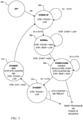
- FIG. 3 is a state diagram illustrating operation of the power management processing module 202 of the PMIC 104 as controlled by the PM control circuit 203 according to one embodiment of the present disclosure.
- the power management processing module 202 converts VIN to SV which is provided to the processor 106, indicates the status of the of SV (e.g., via the STBY_PGOOD pin or the RSTB pin), communicates with the processor 106 via the communication bus 211 (e.g., receiving digital code as part of the two step standby entry process), ensures a maximum duration of the low power mode of the processor 106 (e.g., via the standby timing window counter 208), and detects a request from the processor 106 (e.g., STBY_EXIT) to exit its low power mode and return to the normal mode of operation.
- the processor 106 e.g., STBY_EXIT
- a first OFF state 302 is a state in which the switchable regulators are off (or otherwise held in reset) and the system is in a "safe" state while holding the processor 106 in its off or reset state. Operation transitions to a POWER UP state 304 in response to an ON indication in which the PM control circuit 203 performs a predefined startup sequence including activating one or more switchable regulators in the power converter 206. During the startup sequence while SV is below the high threshold level HVTH, or SV ⁇ HVTH, STBY_PGOOD remains low.
- the PM control circuit 203 transitions to a POWER DOWN state 308 in which it starts the standby timing window counter 208 and begins disabling the switchable regulator(s) of the power converter 206 so that SV begins decreasing. Also, the PM control circuit 203 asserts the STBY_RESP signal high to indicate to the safety processing module 204 that the power management processing module 202 is transitioning to its standby mode.
- the POWER DOWN state 308 is not a complete power down of the PMIC 104 but instead is a state in which power is reduced from the full power normal mode to the low power standby mode.
- the STBY_START signal serves as a standby start indication from the safety control circuit 205 to the PM control circuit 203 for transitioning into the standby mode.
- the STBY_RESP signal serves as a standby response indication from the PM control circuit 203 to the safety control circuit 205 in response to the STBY_START signal. Operation remains in the POWER DOWN state 308 while SV ⁇ LVTH.
- the switchable regulator(s) of the power converter 206 are disabled so that SV ⁇ LVTH, then the PM control circuit 203 transitions to a STANDBY state 310 by placing the power management processing module 202 in its standby mode in which the STBY_PGOOD pin is asserted low.
- the PMIC 104 and the processor 106 are both fully in their respective low power states expending the lowest possible quiescent current for low power operation.
- Operation of the power management processing module 202 remains in its STANDBY state 310 until either the processor 106 asserts STBY_EXIT high to request transition back to the normal mode or upon timeout of the timer standby timing window counter 208. If the standby timing window counter 208 times out during either of the states 308 or 310 before STBY_EXIT is asserted high, then the PM control circuit 203 initiates a full reset and a new power up sequence to reset the entire system, including asserting RSTB low to reset the processor 106.
- the standby timing window counter 208 is programmed with a timing value determining the maximum amount of time to stay in the low power mode to prevent the processor 106 from getting stuck in its low power mode or somehow unable to awake.
- the processor 106 may perform periodic wakeup and power down sequences, such as during longer periods of inactivity or the like, to ensure that the system is ready to power up and perform normal operating functions. If for any reason the processor 106 fails to wakeup the system, timeout of the standby timing window counter 208 causes power cycling of the system.
- the PM control circuit 203 transitions to a STANDBY EXIT state 312 in which it stops the standby timing window counter 208 and begins the power up process.
- the STBY_PGOOD pin remains negated low during the STANDBY EXIT state 312. Operation then transitions back to the POWER UP state 304 in which the PM control circuit 203 performs the predefined startup sequence including activating the switchable regulator(s) of the power converter 206 as previously described.
- SV ⁇ HVTH as previously described, operation once again transitions to the NORMAL state 306 and asserts STBY_PGOOD high to wake up the processor 106.
- FIG. 4 is a state diagram illustrating operation of the safety processing module 204 of the PMIC 104 as controlled by the safety control circuit 205 according to one embodiment of the present disclosure.
- the safety processing module 204 performs integrity testing of the PMIC 104, controls the states of the FSOB and RSTB pins such as freezing the pin states during the standby mode, monitors the state of the FS_STBY_ENTRY pin, resets the processor 106 under certain conditions, monitors SV for overvoltage or undervoltage, times the duration between the two steps of the two step standby entry process to detect a valid standby transition request, times activation of the memory elements of the memory circuit 217, and performs CRC to protect the integrity of communications between the processor 106 and the PMIC 104 via the communication bus 211.
- the safety processing module 204 and the power management processing module 202 operate independently yet in parallel with each other.
- the STBY_START and STBY_RESP signals are handshake signals for controlling transition from the normal mode to the standby mode as
- a first OFF state 402 corresponds with the OFF state 302 of the power management processing module 202.
- the safety control circuit 205 transitions to an LBIST state 404 in which the LBIST circuit 224 is activated to check the integrity of the control logic of the safety processing module 204.
- LBIST OK or LBIST NOK operation transitions to an ABIST state 406 in which the ABIST circuit 226 is activated to check the integrity of the memory circuit 217 and the states of the FS_STBY_ENTRY, FSOB, RSTB pins and analog monitors (not shown).
- the safety control circuit 205 transitions to a NORMAL state 408 of the safety processing module 204 indicating that it is operating in its normal mode.
- the RSTB pin is de-asserted high to enable the processor 106 to power up, and the FSOB pin is also de-asserted high as long as LBIST OK and ABIST OK are both true. Operation remains in the NORMAL state 408 while the processor 106 is in its normal mode and performing its normal functions. If either LBIST NOK or ABIST NOK (either test failed), then entry into the standby mode is not allowed and operation remains in the NORMAL state 408 which prevents the processor 106 from entering its low power mode. It is noted that RSTB may be released to allow the PMIC 104 and the processor 106 to do some additional integrity testing to correct the condition or to indicate error.
- the processor 106 begins the two step standby process by causing the LP entry control circuit 232 to send the digital code to the PMIC 104 via the communication bus 211.
- the PMIC 104 receives the predetermined digital code via the communication bus 211 and stores the digital code into the STBY register 214 of the safety processing module 204. If the safety control circuit 205 determines that the digital code is valid (meaning that it is equal to a predetermined digital code value), and if both LBIST and ABIST integrity tests have passed (LBIST OK and ABIST OK), then operation transitions to a SAFE state 410 in which the safety control circuit 205 starts the standby entry timing counter 216.
- the PMIC 104 prevents the processor 106 from entering the standby mode.
- the FSOB pin which is coupled to the external application safe state logic 240, is asserted low to enter into the safe state of operation. Operation remains in the SAFE state 410 until timeout of the standby entry timing counter 216 or until the FS_STBY_ENTRY pin is asserted low completing the two step standby process.
- the safety control circuit 205 returns operation back to the OFF state 402 and forces a full power down followed by power up of the entire system, which also causes power cycling of the power management processing module 202. Essentially, operation transitions back to OFF state 402 for the safety processing module 204 and back to OFF state 302 of the power management processing module 202 and then the system is powered back up.
- operation may instead return to the NORMAL state 408 with additional assertion of RSTB low to only reset the processor 106 without performing a full power down. Note that RSTB is asserted low during the transition and is then de-asserted back high in the NORMAL state 408 which causes the processor 106 to be reset.
- the safety control circuit 205 transitions to a VALID state 412 in which it asserts the STBY_START signal high causing the power management processing module 202 to transition to the POWER DOWN state 308.
- the safety control circuit 205 also initiates the ACK timing counter 227 in the VALID state 412, and then transitions to a MEMORY state 414 in which it activates the memory circuit 217 to hold the RSTB pin high in its released state and to hold the FSOB pin low to maintain the system in the safe state.
- timeout of the ACK timing counter 227 causes the safety control circuit 205 to return operation back to the OFF state 402 and to force a full power down followed by power up of the entire system, which also causes power cycling of the power management processing module 202.
- operation transitions back to the OFF state 402 for the safety processing module 204 and back to the OFF state 302 of the power management processing module 202 and then the system is powered back up.
- operation may return to the NORMAL state 408 with additional assertion of RSTB low to only reset the processor 106 without performing a full power down.
- the RSTB is asserted low during the transition and is then de-asserted back high in the NORMAL state 408 which causes the processor 106 to be reset.
- operation transitions to a STANDBY state 416 in which the safety control circuit 205 transitions the safety processing module 204 to its standby mode and the ACK timing counter 227 is stopped.
- the safety processing module 204 is powered down in its standby mode except that the memory elements safety processing supply 222 remains minimally powered to power the memory circuit 217 to maintain the states of the RSTB and FSOB pins during the standby mode.
- the safety control circuit 205 When the safety control circuit 205 detects assertion of the STBY_EXIT pin high (such as directly or via another signal in response to STBY_EXIT, not shown), it wakes up and transitions back to the LBIST state 404 to eventually transition to the NORMAL state 408 as previously described. Also, the safety processing module 204 is reset and powered up if the standby timing window counter 208 times out during the standby mode.
- a system and method of power mode management for a processor providing safe and robust transitioning between normal and low power modes to meet low current requirements and to ensure accurate power mode transition communications.
- a two step process includes receiving a digital code, starting a standby entry timer, and receiving a low power request indication before timeout of the standby entry timer to ensure a valid request, and otherwise resetting upon timer timeout.
- a watchdog timer ensures that a maximum standby duration is not exceeded.
- An acknowledge timer ensures valid communication between modules of a power management IC.
- Memory elements ensure and maintain valid states of reset and safe state pins during standby. Self tests are performed in which test failure prevents transition to the low power mode.
- a power good indication ensures the processor that the supply voltages are suitable for both low power and normal operation.
Landscapes
- Engineering & Computer Science (AREA)
- Theoretical Computer Science (AREA)
- General Engineering & Computer Science (AREA)
- Physics & Mathematics (AREA)
- General Physics & Mathematics (AREA)
- Quality & Reliability (AREA)
- Computer Hardware Design (AREA)
- Computing Systems (AREA)
- Power Sources (AREA)
Claims (15)
- Verarbeitungssystem (102), das Folgendes umfasst:
eine Leistungsmanagementschaltung (104), die einen Normalmodus und einen Niederleistungsmodus aufweist, umfassend:ein Leistungsmanagement-Verarbeitungsmodul (202), umfassend:eine Kommunikationsschnittstelle (210); undeine Leistungssteuerungsschaltung (203), die die Leistungsmanagementschaltung aus dem Niederleistungsmodus in den Normalmodus überführt,wenn während des Niederleistungsmodus eine Niederleistung-Verlassen-Anforderung empfangen wird;dadurch gekennzeichnet, dass es Folgendes umfasst:ein Sicherheitsverarbeitungsmodul (204), das Folgendes umfasst:einen Bereitschaftsspeicher (214);einen Bereitschaft-Eintrittstimer (216); undeine Sicherheitssteuerungsschaltung (205), die den Bereitschaft-Eintrittstimer während des Normalmodus auslöst, wenn ein vorbestimmter Digitalwert in den Bereitschaftsspeicher geschrieben wird, und die eine Bereitschaft-Startangabe (STBY_START) liefert, um das Leistungsmanagement-Verarbeitungsmodul in den Niederleistungsmodus nur dann überzuführen,wenn eine Niederleistung-Anforderungsangabe (STBY) vor Zeitablauf des Bereitschaft-Eintrittstimers empfangen wird. - Verarbeitungssystem nach Anspruch 1, wobei die Sicherheitssteuerungsschaltung einen Rücksetzprozess durchführt, wenn der Bereitschaft-Eintrittstimer abläuft, bevor die Bereitschaft-Anforderungsangabe empfangen wird.
- Verarbeitungssystem nach einem vorhergehenden Anspruch, wobei das Leistungsmanagement-Verarbeitungsmodul ferner Folgendes umfasst:einen Leistungswandler (206), der eineVersorgungsspannung liefert; undwobei die Leistungssteuerungsschaltung Herunterfahren des Leistungswandlers auslöst, als Reaktion auf die Bereitschaft-Startangabe von derSicherheitssteuerungsschaltung, und eine Bereitschaft-Antwortangabe (STBY_RESP) liefert.
- Verarbeitungssystem nach Anspruch 3, wobei das Leistungsmanagement-Verarbeitungsmodul ferner Folgendes umfasst:einen Watchdog-Timer (208); undwobei die Leistungssteuerungsschaltung den Watchdog-Timer als Reaktion auf die Bereitschaft-Startangabe von der Sicherheitssteuerungsschaltung startet, wobei die Leistungsverarbeitungsschaltung einen Rücksetzprozess durchführt, wenn der Watchdog-Timer abläuft, und wobei die Leistungssteuerungsschaltung einen Stromversorgung-Gut-Pin bzw. STBY_PGOOD-Pin in einen ersten Zustand,wenn die Versorgungsspannung über einen vorbestimmten Hohe-Schwelle-Pegel geladen ist, und in einen zweiten Zustand, wenn die Versorgungsspannung unter einen vorbestimmten Niedrige-Schwelle-Pegel entladen ist, versetzt.
- Verarbeitungssystem nach Anspruch 4, wobei die Leistungssteuerungsschaltung den Watchdog-Timer stoppt, den Leistungswandler reaktiviert und die Sicherheitssteuerungsschaltung anstößt, das Sicherheitsverarbeitungsmodul als Reaktion auf Empfangen der Niederleistung-Verlassen-Anforderung aufzuwecken.
- Verarbeitungssystem nach einem der Ansprüche 3 bis 5, wobei die Sicherheitsverarbeitungsschaltung einen Bestätigungs-Timer (227) startet, wenn die Bereitschaft-Startangabe geliefert wird, wobei die Sicherheitsverarbeitungsschaltung einen Rücksetzprozess durchführt, wenn der Bestätigungs-Timer abläuft, bevor die Bereitschaft-Antwortangabe geliefert wird, und wobei die Sicherheitsverarbeitungsschaltung in den Niederleistungsmodus eintritt und den Bestätigungs-Timer stoppt, wenn die Bereitschaft-Antwortangabe vor Ablaufen des Bestätigungs-Timers geliefert wird.
- Verarbeitungssystem nach Anspruch 6, wobei das Sicherheitsverarbeitungsmodul ferner mindestens ein Speicherelement (219) umfasst, das einen Zustand von jedem des mindestens einen Pins während des Niederleistungsmodus aufrechterhält.
- Verarbeitungssystem nach einem der Ansprüche 6 oder 7, wobei das Sicherheitsverarbeitungsmodul ferner Folgendes umfasst:eine Testschaltung (224), die einen Selbsttest des Sicherheitsverarbeitungsmoduls während Hochfahrens durchführt und die eine Bestanden-Angabe, die solches angibt, liefert; undwobei die Sicherheitsverarbeitungsschaltung Eintreten in den Bereitschaftsmodus verhindert, wenn die Bestanden-Angabe Test-Fehlgeschlagen angibt.
- Verarbeitungssystem nach einem vorhergehenden Anspruch, ferner umfassend:einen Prozessor (106), der einen Normal-Prozessormodus und einen Niederleistung-Prozessormodus aufweist,wobei der Prozessor Folgendes umfasst:eine Niederleistung-Steuerschaltung (232), die Eintreten in den Niederleistung-Prozessormodus anfordert, indem der vorbestimmte Digitalwert über die Kommunikationsschnittstelle an dieLeistungsmanagementschaltung geliefert wird; und eine Niederleistung-Anforderungsschaltung (236), die die Niederleistung-Anforderungsangabe liefert, nachdem der vorbestimmte Digitalwert geliefert wurde.
- Verarbeitungssystem nach Anspruch 9, wobei der Prozessor ferner eine Niederleistung-Domäne-Schaltung (230) umfasst, die die Niederleistung-Verlassen-Anforderung liefert, um Wiedereintreten in den normalen Verarbeitungsmodus anzufordern, und die Wiedereintreten in den normalen Verarbeitungsmodus nur dann auslöst, wenn ein Stromversorgung-Gut-Pin der Leistungsmanagementschaltung angibt, dass eine Versorgungsspannung über einem vorbestimmten Schwellenpegel liegt.
- Verarbeitungssystem nach Anspruch 10, wobei die Niederleistung-Domäne-Schaltung den Prozessor befähigt zum Übergehen aus dem normalen Verarbeitungsmodus in den Niederleistung-Verarbeitungsmodus nur dann, wenn ein Stromversorgung-Gut-Pin der Leistungsmanagementschaltung angibt, dass eine Versorgungsspannung unter einem vorbestimmten Schwellenpegel liegt.
- Verfahren zum Leistungsmodusmanagement, das Folgendes umfasst:
Übergehen von einem Niederleistungsmodus in einen Normalmodus als Reaktion auf Empfangen einer Niederleistung-Verlassen-Anforderung; gekennzeichnet durch:Empfangen eines Digitalcodes während des normalen Betriebsmodus;Vergleichen des empfangenen Digitalcodes mit einem vorbestimmten Digitalwert;Auslösen eines Bereitschaft-Eintrittstimers, wenn der empfangene Digitalcode mit dem vorbestimmten Digitalwert übereinstimmt;Liefern einer Bereitschaft-Startangabe zum Beginnen des Übergehens in den Niederleistungsbetriebsmodus aus dem Normalmodus nur dann, wenn eine Bereitschaft-Anforderungsangabe vor Ablaufen des Bereitschaft-Eintrittstimers empfangen wird. - Verfahren nach Anspruch 12, ferner umfassend Durchführen eines Rücksetzprozesses, wenn der Bereitschaft-Eintrittstimer abläuft, bevor die Niederleistung-Anforderungsangabe empfangen wird.
- Verfahren nach Anspruch 12 oder 13, ferner umfassend:
Bereitstellen einer Versorgungsspannung; und als Reaktion auf Empfangen der Bereitschaft-Startangabe, Entladen der Versorgungsspannung und Liefern einer Bereitschaft-Antwortangabe. - Verfahren nach einem der Ansprüche 12 bis 14, ferner umfassend:Anfordern, durch einen Prozessor, von Eintreten in den Niederleistungsmodus durch Liefern des Digitalcodes während des Normalmodus;Liefern, durch den Prozessor, der Niederleistung-Anforderung, nachdem der Digitalcode geliefert wurde;Eintreten in den Niederleistungsmodus, durch den Prozessor, wenn eine Stromversorgung-Gut-Angabe angibt,dass eine Versorgungsspannung unter einem vorbestimmten Niedrige-Schwelle-Pegel liegt;Anfordern, durch den Prozessor, von Eintritt in den Normalmodus durch Liefern der Niederleistung-Verlassen-Anforderung; undEintreten in den Normalmodus, durch den Prozessor, wenn die Stromversorgung-Gut-Angabe angibt, dass die Versorgungsspannung über einem vorbestimmten Hohe-Schwelle-Pegel liegt.
Priority Applications (3)
| Application Number | Priority Date | Filing Date | Title |
|---|---|---|---|
| EP19305638.9A EP3742257B1 (de) | 2019-05-20 | 2019-05-20 | System und verfahren zur leistungsmodusverwaltung für einen prozessor |
| CN202010292988.9A CN111966196B (zh) | 2019-05-20 | 2020-04-15 | 用于处理器的电源模式管理的系统和方法 |
| US16/852,936 US11175723B2 (en) | 2019-05-20 | 2020-04-20 | System and method of power mode management for a processor |
Applications Claiming Priority (1)
| Application Number | Priority Date | Filing Date | Title |
|---|---|---|---|
| EP19305638.9A EP3742257B1 (de) | 2019-05-20 | 2019-05-20 | System und verfahren zur leistungsmodusverwaltung für einen prozessor |
Publications (2)
| Publication Number | Publication Date |
|---|---|
| EP3742257A1 EP3742257A1 (de) | 2020-11-25 |
| EP3742257B1 true EP3742257B1 (de) | 2022-02-16 |
Family
ID=67902430
Family Applications (1)
| Application Number | Title | Priority Date | Filing Date |
|---|---|---|---|
| EP19305638.9A Active EP3742257B1 (de) | 2019-05-20 | 2019-05-20 | System und verfahren zur leistungsmodusverwaltung für einen prozessor |
Country Status (3)
| Country | Link |
|---|---|
| US (1) | US11175723B2 (de) |
| EP (1) | EP3742257B1 (de) |
| CN (1) | CN111966196B (de) |
Families Citing this family (13)
| Publication number | Priority date | Publication date | Assignee | Title |
|---|---|---|---|---|
| US12299443B2 (en) * | 2018-06-11 | 2025-05-13 | Traxen Inc. | Safety supervised general purpose computing devices |
| CN111221402A (zh) * | 2018-11-26 | 2020-06-02 | 超威半导体(上海)有限公司 | 多层低功率状态 |
| US11709500B2 (en) | 2020-04-14 | 2023-07-25 | Samsara Inc. | Gateway system with multiple modes of operation in a fleet management system |
| US11983423B2 (en) * | 2021-03-17 | 2024-05-14 | Micron Technology, Inc. | Host recovery for a stuck condition |
| US12097777B2 (en) | 2021-06-04 | 2024-09-24 | Geotab Inc. | Methods and systems for predicting a potential alternator failure |
| US11487315B1 (en) * | 2021-09-30 | 2022-11-01 | Geotab Inc. | Method and system for impact detection in a stationary vehicle |
| US11623534B2 (en) | 2021-06-04 | 2023-04-11 | Geotab Inc. | Systems and methods for determining a vehicle alternator condition |
| CN113438141B (zh) * | 2021-06-21 | 2023-04-25 | 扬州以太智能科技有限公司 | 一种数字接收模块的智能化状态监测方法 |
| US11586269B1 (en) | 2021-09-30 | 2023-02-21 | Geotab Inc. | Method and system for impact detection in a stationary vehicle |
| US12025632B2 (en) | 2021-09-30 | 2024-07-02 | Geotab Inc. | Low-power acceleration detection in a telematics device |
| EP4350481A1 (de) * | 2022-10-05 | 2024-04-10 | NXP USA, Inc. | Verarbeitung von aufweckanfragen unter verwendung eines verarbeitungssystems mit leistungsverwaltungsschaltung und verarbeitungsschaltung |
| US12124309B2 (en) | 2022-11-16 | 2024-10-22 | Nxp Usa, Inc. | Fault detection during entry to or exit from low power mode |
| US20240411354A1 (en) * | 2023-06-08 | 2024-12-12 | Nxp Usa, Inc. | Transitions between low power modes in a processing system |
Family Cites Families (16)
| Publication number | Priority date | Publication date | Assignee | Title |
|---|---|---|---|---|
| US6112320A (en) * | 1997-10-29 | 2000-08-29 | Dien; Ghing-Hsin | Computer watchdog timer |
| US6950951B2 (en) * | 2002-04-30 | 2005-09-27 | Arm Limited | Power control signalling |
| US20040103345A1 (en) * | 2002-11-21 | 2004-05-27 | Dunstan Robert A. | Method, apparatus and system for ensuring reliable power down of a personal computer |
| US7315952B2 (en) * | 2004-06-02 | 2008-01-01 | Intel Corporation | Power state coordination between devices sharing power-managed resources |
| EP1882219A2 (de) * | 2005-05-10 | 2008-01-30 | Nxp B.V. | Sleep-watchdog-schaltung für asynchrone digitale schaltungen |
| US7952401B2 (en) * | 2008-10-24 | 2011-05-31 | Freescale Semiconductor, Inc. | Standby control circuit and method |
| US8156275B2 (en) * | 2009-05-13 | 2012-04-10 | Apple Inc. | Power managed lock optimization |
| US8054120B2 (en) * | 2009-06-30 | 2011-11-08 | Stmicroelectronics Design & Application Gmbh | Integrated circuit operable in a standby mode |
| GB2472050B (en) * | 2009-07-22 | 2013-06-19 | Wolfson Microelectronics Plc | Power management apparatus and methods |
| GB2487945A (en) * | 2011-02-10 | 2012-08-15 | Jaguar Cars | Motor Vehicle Shutdown Control |
| US10126803B1 (en) * | 2011-04-04 | 2018-11-13 | Google Llc | Conditional power management activities |
| US8615610B2 (en) * | 2011-09-29 | 2013-12-24 | Freescale Semiconductor, Inc. | Interface system and method with backward compatibility |
| US9218044B2 (en) * | 2012-11-27 | 2015-12-22 | International Business Machines Corporation | Computing system frequency target monitor |
| US9411394B2 (en) * | 2013-03-15 | 2016-08-09 | Seagate Technology Llc | PHY based wake up from low power mode operation |
| US9426748B2 (en) | 2014-07-11 | 2016-08-23 | Qualcomm Incorporated | Dynamic sleep mode based upon battery charge |
| JP6430896B2 (ja) * | 2015-06-05 | 2018-11-28 | アルパイン株式会社 | 電子機器のスタンバイ処理制御装置およびスタンバイ処理制御方法 |
-
2019
- 2019-05-20 EP EP19305638.9A patent/EP3742257B1/de active Active
-
2020
- 2020-04-15 CN CN202010292988.9A patent/CN111966196B/zh active Active
- 2020-04-20 US US16/852,936 patent/US11175723B2/en active Active
Also Published As
| Publication number | Publication date |
|---|---|
| EP3742257A1 (de) | 2020-11-25 |
| CN111966196B (zh) | 2025-04-25 |
| US20200371581A1 (en) | 2020-11-26 |
| US11175723B2 (en) | 2021-11-16 |
| CN111966196A (zh) | 2020-11-20 |
Similar Documents
| Publication | Publication Date | Title |
|---|---|---|
| EP3742257B1 (de) | System und verfahren zur leistungsmodusverwaltung für einen prozessor | |
| US10346231B2 (en) | Watchdog circuit, power IC and watchdog monitor system | |
| US6944779B2 (en) | Power management fault strategy for automotive multimedia system | |
| US7774648B2 (en) | Microprocessor supervision in a special purpose computer system | |
| EP3796128B1 (de) | Leistungsmodusübergangsverwaltung für leistungsversorgung | |
| EP2843502B1 (de) | Informationsverarbeitungsvorrichtung, informationsverarbeitungsverfahren und programm | |
| US9471140B2 (en) | Valid context status retention in processor power mode management | |
| US12332724B2 (en) | Processing wakeup requests in a processing system having power management circuitry and a processing circuitry | |
| US11216053B2 (en) | Systems, apparatus, and methods for transitioning between multiple operating states | |
| US20240411354A1 (en) | Transitions between low power modes in a processing system | |
| US8423802B2 (en) | Power scaling module and power scaling unit of an electronic system having a function unit in a standby state which is insensitive to change in frequency or voltage during synchronization | |
| US12386406B2 (en) | Power supply system for detecting a rail violation in a multi-rail sequence | |
| US20100332902A1 (en) | Power efficient watchdog service | |
| JP5281625B2 (ja) | コンピュータのリセット方法およびコンピュータ | |
| US20100332874A1 (en) | Microcomputer and microcomputer system | |
| JPH07114401A (ja) | Ramバックアップ回路 | |
| US11847466B2 (en) | Controlled thermal shutdown and recovery | |
| CN120517338A (zh) | 差速锁控制器的控制方法和车辆 | |
| CN113650498A (zh) | 一种电动车的上电方法、装置、电动车及存储介质 | |
| JPH09212201A (ja) | 生産設備用制御回路 | |
| JPH0961470A (ja) | 停電処理方法及びその装置 |
Legal Events
| Date | Code | Title | Description |
|---|---|---|---|
| PUAI | Public reference made under article 153(3) epc to a published international application that has entered the european phase |
Free format text: ORIGINAL CODE: 0009012 |
|
| STAA | Information on the status of an ep patent application or granted ep patent |
Free format text: STATUS: THE APPLICATION HAS BEEN PUBLISHED |
|
| AK | Designated contracting states |
Kind code of ref document: A1 Designated state(s): AL AT BE BG CH CY CZ DE DK EE ES FI FR GB GR HR HU IE IS IT LI LT LU LV MC MK MT NL NO PL PT RO RS SE SI SK SM TR |
|
| AX | Request for extension of the european patent |
Extension state: BA ME |
|
| STAA | Information on the status of an ep patent application or granted ep patent |
Free format text: STATUS: REQUEST FOR EXAMINATION WAS MADE |
|
| 17P | Request for examination filed |
Effective date: 20210525 |
|
| RBV | Designated contracting states (corrected) |
Designated state(s): AL AT BE BG CH CY CZ DE DK EE ES FI FR GB GR HR HU IE IS IT LI LT LU LV MC MK MT NL NO PL PT RO RS SE SI SK SM TR |
|
| GRAP | Despatch of communication of intention to grant a patent |
Free format text: ORIGINAL CODE: EPIDOSNIGR1 |
|
| STAA | Information on the status of an ep patent application or granted ep patent |
Free format text: STATUS: GRANT OF PATENT IS INTENDED |
|
| GRAJ | Information related to disapproval of communication of intention to grant by the applicant or resumption of examination proceedings by the epo deleted |
Free format text: ORIGINAL CODE: EPIDOSDIGR1 |
|
| GRAP | Despatch of communication of intention to grant a patent |
Free format text: ORIGINAL CODE: EPIDOSNIGR1 |
|
| INTG | Intention to grant announced |
Effective date: 20211013 |
|
| INTG | Intention to grant announced |
Effective date: 20211027 |
|
| GRAS | Grant fee paid |
Free format text: ORIGINAL CODE: EPIDOSNIGR3 |
|
| GRAA | (expected) grant |
Free format text: ORIGINAL CODE: 0009210 |
|
| STAA | Information on the status of an ep patent application or granted ep patent |
Free format text: STATUS: THE PATENT HAS BEEN GRANTED |
|
| AK | Designated contracting states |
Kind code of ref document: B1 Designated state(s): AL AT BE BG CH CY CZ DE DK EE ES FI FR GB GR HR HU IE IS IT LI LT LU LV MC MK MT NL NO PL PT RO RS SE SI SK SM TR |
|
| REG | Reference to a national code |
Ref country code: GB Ref legal event code: FG4D |
|
| REG | Reference to a national code |
Ref country code: CH Ref legal event code: EP |
|
| REG | Reference to a national code |
Ref country code: DE Ref legal event code: R096 Ref document number: 602019011660 Country of ref document: DE |
|
| REG | Reference to a national code |
Ref country code: AT Ref legal event code: REF Ref document number: 1469297 Country of ref document: AT Kind code of ref document: T Effective date: 20220315 |
|
| REG | Reference to a national code |
Ref country code: IE Ref legal event code: FG4D |
|
| REG | Reference to a national code |
Ref country code: LT Ref legal event code: MG9D |
|
| REG | Reference to a national code |
Ref country code: NL Ref legal event code: MP Effective date: 20220216 |
|
| REG | Reference to a national code |
Ref country code: AT Ref legal event code: MK05 Ref document number: 1469297 Country of ref document: AT Kind code of ref document: T Effective date: 20220216 |
|
| PG25 | Lapsed in a contracting state [announced via postgrant information from national office to epo] |
Ref country code: SE Free format text: LAPSE BECAUSE OF FAILURE TO SUBMIT A TRANSLATION OF THE DESCRIPTION OR TO PAY THE FEE WITHIN THE PRESCRIBED TIME-LIMIT Effective date: 20220216 Ref country code: RS Free format text: LAPSE BECAUSE OF FAILURE TO SUBMIT A TRANSLATION OF THE DESCRIPTION OR TO PAY THE FEE WITHIN THE PRESCRIBED TIME-LIMIT Effective date: 20220216 Ref country code: PT Free format text: LAPSE BECAUSE OF FAILURE TO SUBMIT A TRANSLATION OF THE DESCRIPTION OR TO PAY THE FEE WITHIN THE PRESCRIBED TIME-LIMIT Effective date: 20220616 Ref country code: NO Free format text: LAPSE BECAUSE OF FAILURE TO SUBMIT A TRANSLATION OF THE DESCRIPTION OR TO PAY THE FEE WITHIN THE PRESCRIBED TIME-LIMIT Effective date: 20220516 Ref country code: NL Free format text: LAPSE BECAUSE OF FAILURE TO SUBMIT A TRANSLATION OF THE DESCRIPTION OR TO PAY THE FEE WITHIN THE PRESCRIBED TIME-LIMIT Effective date: 20220216 Ref country code: LT Free format text: LAPSE BECAUSE OF FAILURE TO SUBMIT A TRANSLATION OF THE DESCRIPTION OR TO PAY THE FEE WITHIN THE PRESCRIBED TIME-LIMIT Effective date: 20220216 Ref country code: HR Free format text: LAPSE BECAUSE OF FAILURE TO SUBMIT A TRANSLATION OF THE DESCRIPTION OR TO PAY THE FEE WITHIN THE PRESCRIBED TIME-LIMIT Effective date: 20220216 Ref country code: ES Free format text: LAPSE BECAUSE OF FAILURE TO SUBMIT A TRANSLATION OF THE DESCRIPTION OR TO PAY THE FEE WITHIN THE PRESCRIBED TIME-LIMIT Effective date: 20220216 Ref country code: BG Free format text: LAPSE BECAUSE OF FAILURE TO SUBMIT A TRANSLATION OF THE DESCRIPTION OR TO PAY THE FEE WITHIN THE PRESCRIBED TIME-LIMIT Effective date: 20220516 |
|
| PG25 | Lapsed in a contracting state [announced via postgrant information from national office to epo] |
Ref country code: PL Free format text: LAPSE BECAUSE OF FAILURE TO SUBMIT A TRANSLATION OF THE DESCRIPTION OR TO PAY THE FEE WITHIN THE PRESCRIBED TIME-LIMIT Effective date: 20220216 Ref country code: LV Free format text: LAPSE BECAUSE OF FAILURE TO SUBMIT A TRANSLATION OF THE DESCRIPTION OR TO PAY THE FEE WITHIN THE PRESCRIBED TIME-LIMIT Effective date: 20220216 Ref country code: GR Free format text: LAPSE BECAUSE OF FAILURE TO SUBMIT A TRANSLATION OF THE DESCRIPTION OR TO PAY THE FEE WITHIN THE PRESCRIBED TIME-LIMIT Effective date: 20220517 Ref country code: FI Free format text: LAPSE BECAUSE OF FAILURE TO SUBMIT A TRANSLATION OF THE DESCRIPTION OR TO PAY THE FEE WITHIN THE PRESCRIBED TIME-LIMIT Effective date: 20220216 Ref country code: AT Free format text: LAPSE BECAUSE OF FAILURE TO SUBMIT A TRANSLATION OF THE DESCRIPTION OR TO PAY THE FEE WITHIN THE PRESCRIBED TIME-LIMIT Effective date: 20220216 |
|
| PG25 | Lapsed in a contracting state [announced via postgrant information from national office to epo] |
Ref country code: IS Free format text: LAPSE BECAUSE OF FAILURE TO SUBMIT A TRANSLATION OF THE DESCRIPTION OR TO PAY THE FEE WITHIN THE PRESCRIBED TIME-LIMIT Effective date: 20220617 |
|
| PG25 | Lapsed in a contracting state [announced via postgrant information from national office to epo] |
Ref country code: SM Free format text: LAPSE BECAUSE OF FAILURE TO SUBMIT A TRANSLATION OF THE DESCRIPTION OR TO PAY THE FEE WITHIN THE PRESCRIBED TIME-LIMIT Effective date: 20220216 Ref country code: SK Free format text: LAPSE BECAUSE OF FAILURE TO SUBMIT A TRANSLATION OF THE DESCRIPTION OR TO PAY THE FEE WITHIN THE PRESCRIBED TIME-LIMIT Effective date: 20220216 Ref country code: RO Free format text: LAPSE BECAUSE OF FAILURE TO SUBMIT A TRANSLATION OF THE DESCRIPTION OR TO PAY THE FEE WITHIN THE PRESCRIBED TIME-LIMIT Effective date: 20220216 Ref country code: EE Free format text: LAPSE BECAUSE OF FAILURE TO SUBMIT A TRANSLATION OF THE DESCRIPTION OR TO PAY THE FEE WITHIN THE PRESCRIBED TIME-LIMIT Effective date: 20220216 Ref country code: DK Free format text: LAPSE BECAUSE OF FAILURE TO SUBMIT A TRANSLATION OF THE DESCRIPTION OR TO PAY THE FEE WITHIN THE PRESCRIBED TIME-LIMIT Effective date: 20220216 Ref country code: CZ Free format text: LAPSE BECAUSE OF FAILURE TO SUBMIT A TRANSLATION OF THE DESCRIPTION OR TO PAY THE FEE WITHIN THE PRESCRIBED TIME-LIMIT Effective date: 20220216 |
|
| REG | Reference to a national code |
Ref country code: DE Ref legal event code: R097 Ref document number: 602019011660 Country of ref document: DE |
|
| PG25 | Lapsed in a contracting state [announced via postgrant information from national office to epo] |
Ref country code: AL Free format text: LAPSE BECAUSE OF FAILURE TO SUBMIT A TRANSLATION OF THE DESCRIPTION OR TO PAY THE FEE WITHIN THE PRESCRIBED TIME-LIMIT Effective date: 20220216 |
|
| PLBE | No opposition filed within time limit |
Free format text: ORIGINAL CODE: 0009261 |
|
| STAA | Information on the status of an ep patent application or granted ep patent |
Free format text: STATUS: NO OPPOSITION FILED WITHIN TIME LIMIT |
|
| REG | Reference to a national code |
Ref country code: CH Ref legal event code: PL |
|
| REG | Reference to a national code |
Ref country code: BE Ref legal event code: MM Effective date: 20220531 |
|
| 26N | No opposition filed |
Effective date: 20221117 |
|
| PG25 | Lapsed in a contracting state [announced via postgrant information from national office to epo] |
Ref country code: MC Free format text: LAPSE BECAUSE OF FAILURE TO SUBMIT A TRANSLATION OF THE DESCRIPTION OR TO PAY THE FEE WITHIN THE PRESCRIBED TIME-LIMIT Effective date: 20220216 Ref country code: LU Free format text: LAPSE BECAUSE OF NON-PAYMENT OF DUE FEES Effective date: 20220520 Ref country code: LI Free format text: LAPSE BECAUSE OF NON-PAYMENT OF DUE FEES Effective date: 20220531 Ref country code: CH Free format text: LAPSE BECAUSE OF NON-PAYMENT OF DUE FEES Effective date: 20220531 |
|
| PG25 | Lapsed in a contracting state [announced via postgrant information from national office to epo] |
Ref country code: SI Free format text: LAPSE BECAUSE OF FAILURE TO SUBMIT A TRANSLATION OF THE DESCRIPTION OR TO PAY THE FEE WITHIN THE PRESCRIBED TIME-LIMIT Effective date: 20220216 |
|
| PG25 | Lapsed in a contracting state [announced via postgrant information from national office to epo] |
Ref country code: IE Free format text: LAPSE BECAUSE OF NON-PAYMENT OF DUE FEES Effective date: 20220520 Ref country code: FR Free format text: LAPSE BECAUSE OF NON-PAYMENT OF DUE FEES Effective date: 20220531 |
|
| PG25 | Lapsed in a contracting state [announced via postgrant information from national office to epo] |
Ref country code: BE Free format text: LAPSE BECAUSE OF NON-PAYMENT OF DUE FEES Effective date: 20220531 |
|
| PG25 | Lapsed in a contracting state [announced via postgrant information from national office to epo] |
Ref country code: IT Free format text: LAPSE BECAUSE OF FAILURE TO SUBMIT A TRANSLATION OF THE DESCRIPTION OR TO PAY THE FEE WITHIN THE PRESCRIBED TIME-LIMIT Effective date: 20220216 |
|
| P01 | Opt-out of the competence of the unified patent court (upc) registered |
Effective date: 20230725 |
|
| PG25 | Lapsed in a contracting state [announced via postgrant information from national office to epo] |
Ref country code: MK Free format text: LAPSE BECAUSE OF FAILURE TO SUBMIT A TRANSLATION OF THE DESCRIPTION OR TO PAY THE FEE WITHIN THE PRESCRIBED TIME-LIMIT Effective date: 20220216 Ref country code: CY Free format text: LAPSE BECAUSE OF FAILURE TO SUBMIT A TRANSLATION OF THE DESCRIPTION OR TO PAY THE FEE WITHIN THE PRESCRIBED TIME-LIMIT Effective date: 20220216 |
|
| PG25 | Lapsed in a contracting state [announced via postgrant information from national office to epo] |
Ref country code: HU Free format text: LAPSE BECAUSE OF FAILURE TO SUBMIT A TRANSLATION OF THE DESCRIPTION OR TO PAY THE FEE WITHIN THE PRESCRIBED TIME-LIMIT; INVALID AB INITIO Effective date: 20190520 |
|
| PG25 | Lapsed in a contracting state [announced via postgrant information from national office to epo] |
Ref country code: TR Free format text: LAPSE BECAUSE OF FAILURE TO SUBMIT A TRANSLATION OF THE DESCRIPTION OR TO PAY THE FEE WITHIN THE PRESCRIBED TIME-LIMIT Effective date: 20220216 |
|
| PG25 | Lapsed in a contracting state [announced via postgrant information from national office to epo] |
Ref country code: MT Free format text: LAPSE BECAUSE OF FAILURE TO SUBMIT A TRANSLATION OF THE DESCRIPTION OR TO PAY THE FEE WITHIN THE PRESCRIBED TIME-LIMIT Effective date: 20220216 |
|
| PGFP | Annual fee paid to national office [announced via postgrant information from national office to epo] |
Ref country code: DE Payment date: 20250423 Year of fee payment: 7 |
|
| PGFP | Annual fee paid to national office [announced via postgrant information from national office to epo] |
Ref country code: GB Payment date: 20250423 Year of fee payment: 7 |