EP3745456A1 - Couches de condensateur de découplage montées perpendiculairement entre une puce à semi-conducteur et un substrat - Google Patents
Couches de condensateur de découplage montées perpendiculairement entre une puce à semi-conducteur et un substrat Download PDFInfo
- Publication number
- EP3745456A1 EP3745456A1 EP19176847.2A EP19176847A EP3745456A1 EP 3745456 A1 EP3745456 A1 EP 3745456A1 EP 19176847 A EP19176847 A EP 19176847A EP 3745456 A1 EP3745456 A1 EP 3745456A1
- Authority
- EP
- European Patent Office
- Prior art keywords
- capacitor
- substrate
- terminals
- decoupling capacitor
- layer
- Prior art date
- Legal status (The legal status is an assumption and is not a legal conclusion. Google has not performed a legal analysis and makes no representation as to the accuracy of the status listed.)
- Withdrawn
Links
Images

Classifications
-
- H—ELECTRICITY
- H10—SEMICONDUCTOR DEVICES; ELECTRIC SOLID-STATE DEVICES NOT OTHERWISE PROVIDED FOR
- H10W—GENERIC PACKAGES, INTERCONNECTIONS, CONNECTORS OR OTHER CONSTRUCTIONAL DETAILS OF DEVICES COVERED BY CLASS H10
- H10W70/00—Package substrates; Interposers; Redistribution layers [RDL]
- H10W70/60—Insulating or insulated package substrates; Interposers; Redistribution layers
- H10W70/67—Insulating or insulated package substrates; Interposers; Redistribution layers characterised by their insulating layers or insulating parts
- H10W70/68—Shapes or dispositions thereof
- H10W70/685—Shapes or dispositions thereof comprising multiple insulating layers
-
- H—ELECTRICITY
- H01—ELECTRIC ELEMENTS
- H01G—CAPACITORS; CAPACITORS, RECTIFIERS, DETECTORS, SWITCHING DEVICES, LIGHT-SENSITIVE OR TEMPERATURE-SENSITIVE DEVICES OF THE ELECTROLYTIC TYPE
- H01G4/00—Fixed capacitors; Processes of their manufacture
- H01G4/002—Details
- H01G4/005—Electrodes
- H01G4/012—Form of non-self-supporting electrodes
-
- H—ELECTRICITY
- H01—ELECTRIC ELEMENTS
- H01G—CAPACITORS; CAPACITORS, RECTIFIERS, DETECTORS, SWITCHING DEVICES, LIGHT-SENSITIVE OR TEMPERATURE-SENSITIVE DEVICES OF THE ELECTROLYTIC TYPE
- H01G4/00—Fixed capacitors; Processes of their manufacture
- H01G4/30—Stacked capacitors
-
- H—ELECTRICITY
- H01—ELECTRIC ELEMENTS
- H01G—CAPACITORS; CAPACITORS, RECTIFIERS, DETECTORS, SWITCHING DEVICES, LIGHT-SENSITIVE OR TEMPERATURE-SENSITIVE DEVICES OF THE ELECTROLYTIC TYPE
- H01G4/00—Fixed capacitors; Processes of their manufacture
- H01G4/40—Structural combinations of fixed capacitors with other electric elements, the structure mainly consisting of a capacitor, e.g. RC combinations
-
- H—ELECTRICITY
- H10—SEMICONDUCTOR DEVICES; ELECTRIC SOLID-STATE DEVICES NOT OTHERWISE PROVIDED FOR
- H10W—GENERIC PACKAGES, INTERCONNECTIONS, CONNECTORS OR OTHER CONSTRUCTIONAL DETAILS OF DEVICES COVERED BY CLASS H10
- H10W70/00—Package substrates; Interposers; Redistribution layers [RDL]
- H10W70/60—Insulating or insulated package substrates; Interposers; Redistribution layers
- H10W70/62—Insulating or insulated package substrates; Interposers; Redistribution layers characterised by their interconnections
- H10W70/65—Shapes or dispositions of interconnections
- H10W70/654—Top-view layouts
- H10W70/655—Fan-out layouts
-
- H—ELECTRICITY
- H10—SEMICONDUCTOR DEVICES; ELECTRIC SOLID-STATE DEVICES NOT OTHERWISE PROVIDED FOR
- H10W—GENERIC PACKAGES, INTERCONNECTIONS, CONNECTORS OR OTHER CONSTRUCTIONAL DETAILS OF DEVICES COVERED BY CLASS H10
- H10W70/00—Package substrates; Interposers; Redistribution layers [RDL]
- H10W70/60—Insulating or insulated package substrates; Interposers; Redistribution layers
- H10W70/67—Insulating or insulated package substrates; Interposers; Redistribution layers characterised by their insulating layers or insulating parts
- H10W70/68—Shapes or dispositions thereof
- H10W70/682—Shapes or dispositions thereof comprising holes having chips therein
-
- H—ELECTRICITY
- H10—SEMICONDUCTOR DEVICES; ELECTRIC SOLID-STATE DEVICES NOT OTHERWISE PROVIDED FOR
- H10W—GENERIC PACKAGES, INTERCONNECTIONS, CONNECTORS OR OTHER CONSTRUCTIONAL DETAILS OF DEVICES COVERED BY CLASS H10
- H10W72/00—Interconnections or connectors in packages
-
- H—ELECTRICITY
- H10—SEMICONDUCTOR DEVICES; ELECTRIC SOLID-STATE DEVICES NOT OTHERWISE PROVIDED FOR
- H10W—GENERIC PACKAGES, INTERCONNECTIONS, CONNECTORS OR OTHER CONSTRUCTIONAL DETAILS OF DEVICES COVERED BY CLASS H10
- H10W72/00—Interconnections or connectors in packages
- H10W72/071—Connecting or disconnecting
- H10W72/072—Connecting or disconnecting of bump connectors
-
- H—ELECTRICITY
- H10—SEMICONDUCTOR DEVICES; ELECTRIC SOLID-STATE DEVICES NOT OTHERWISE PROVIDED FOR
- H10W—GENERIC PACKAGES, INTERCONNECTIONS, CONNECTORS OR OTHER CONSTRUCTIONAL DETAILS OF DEVICES COVERED BY CLASS H10
- H10W72/00—Interconnections or connectors in packages
- H10W72/071—Connecting or disconnecting
- H10W72/072—Connecting or disconnecting of bump connectors
- H10W72/07231—Techniques
- H10W72/07236—Soldering or alloying
-
- H—ELECTRICITY
- H10—SEMICONDUCTOR DEVICES; ELECTRIC SOLID-STATE DEVICES NOT OTHERWISE PROVIDED FOR
- H10W—GENERIC PACKAGES, INTERCONNECTIONS, CONNECTORS OR OTHER CONSTRUCTIONAL DETAILS OF DEVICES COVERED BY CLASS H10
- H10W72/00—Interconnections or connectors in packages
- H10W72/071—Connecting or disconnecting
- H10W72/072—Connecting or disconnecting of bump connectors
- H10W72/07251—Connecting or disconnecting of bump connectors characterised by changes in properties of the bump connectors during connecting
- H10W72/07254—Connecting or disconnecting of bump connectors characterised by changes in properties of the bump connectors during connecting changes in dispositions
-
- H—ELECTRICITY
- H10—SEMICONDUCTOR DEVICES; ELECTRIC SOLID-STATE DEVICES NOT OTHERWISE PROVIDED FOR
- H10W—GENERIC PACKAGES, INTERCONNECTIONS, CONNECTORS OR OTHER CONSTRUCTIONAL DETAILS OF DEVICES COVERED BY CLASS H10
- H10W72/00—Interconnections or connectors in packages
- H10W72/20—Bump connectors, e.g. solder bumps or copper pillars; Dummy bumps; Thermal bumps
- H10W72/241—Dispositions, e.g. layouts
-
- H—ELECTRICITY
- H10—SEMICONDUCTOR DEVICES; ELECTRIC SOLID-STATE DEVICES NOT OTHERWISE PROVIDED FOR
- H10W—GENERIC PACKAGES, INTERCONNECTIONS, CONNECTORS OR OTHER CONSTRUCTIONAL DETAILS OF DEVICES COVERED BY CLASS H10
- H10W72/00—Interconnections or connectors in packages
- H10W72/20—Bump connectors, e.g. solder bumps or copper pillars; Dummy bumps; Thermal bumps
- H10W72/241—Dispositions, e.g. layouts
- H10W72/247—Dispositions of multiple bumps
-
- H—ELECTRICITY
- H10—SEMICONDUCTOR DEVICES; ELECTRIC SOLID-STATE DEVICES NOT OTHERWISE PROVIDED FOR
- H10W—GENERIC PACKAGES, INTERCONNECTIONS, CONNECTORS OR OTHER CONSTRUCTIONAL DETAILS OF DEVICES COVERED BY CLASS H10
- H10W72/00—Interconnections or connectors in packages
- H10W72/20—Bump connectors, e.g. solder bumps or copper pillars; Dummy bumps; Thermal bumps
- H10W72/251—Materials
- H10W72/252—Materials comprising solid metals or solid metalloids, e.g. PbSn, Ag or Cu
-
- H—ELECTRICITY
- H10—SEMICONDUCTOR DEVICES; ELECTRIC SOLID-STATE DEVICES NOT OTHERWISE PROVIDED FOR
- H10W—GENERIC PACKAGES, INTERCONNECTIONS, CONNECTORS OR OTHER CONSTRUCTIONAL DETAILS OF DEVICES COVERED BY CLASS H10
- H10W90/00—Package configurations
- H10W90/701—Package configurations characterised by the relative positions of pads or connectors relative to package parts
- H10W90/721—Package configurations characterised by the relative positions of pads or connectors relative to package parts of bump connectors
- H10W90/724—Package configurations characterised by the relative positions of pads or connectors relative to package parts of bump connectors between a chip and a stacked insulating package substrate, interposer or RDL
-
- H—ELECTRICITY
- H10—SEMICONDUCTOR DEVICES; ELECTRIC SOLID-STATE DEVICES NOT OTHERWISE PROVIDED FOR
- H10W—GENERIC PACKAGES, INTERCONNECTIONS, CONNECTORS OR OTHER CONSTRUCTIONAL DETAILS OF DEVICES COVERED BY CLASS H10
- H10W90/00—Package configurations
- H10W90/701—Package configurations characterised by the relative positions of pads or connectors relative to package parts
- H10W90/721—Package configurations characterised by the relative positions of pads or connectors relative to package parts of bump connectors
- H10W90/728—Package configurations characterised by the relative positions of pads or connectors relative to package parts of bump connectors between a chip and a stacked discrete passive device, e.g. resistors, capacitors or inductors
Definitions
- the present invention relates to a multi layer ceramic capacitor and semiconductor chip carrier package system, more particularly a capacitor embedded into substrate and attached to a semiconductor chip.
- a change in switching activity of logic gates in a semiconductor device causes noise on power and ground lines.
- the power and ground noise leads to performance degradation.
- the power and ground noise is commonly reduced by the employment of decoupling capacitors.
- the ideal connection between the semiconductor device and the decoupling capacitor is without any resistance and inductance. In an actual package this connection is typically as short as possible to reduce parasitic effects that cause unwanted resistance and inductance.
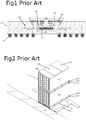
- the substrate 104 of such a package contains wires for power, ground and data signals 108. Near the semiconductor chip there is often a very high wire congestion. When embedding a decoupling capacitor 100 near the semiconductor chip, the required cavity blocks valuable routing space 109 for many wires.
- a multi layer ceramic capacitor ( Fig2 ) have two poles 202 and 203 .
- Each pole comprising a plurality of conducting layers.
- the layers of both poles are isolated by dielectric layers 205 .
- Each pole can have a plurality of terminals that connect to the outside. The advantage of multiple terminals is also to reduce parasitic effects that cause unwanted resistance and inductance.
- An additional object of the invention is to connect two power networks and signal layers of different grid size or pin pitch.
- a decoupling capacitor embedded into the substrate The capacitor is connected to silicon chip and to substrate.
- the capacitor has a dense array of terminals on the side facing the silicon chip.
- the sides facing the substrate have terminals with a lower pin pitch or at least two terminals.
- the multiple terminals on the silicon chip side as well as the short distance to the silicon chip both have the advantage to reduce parasitic effects and both lower the unwanted resistance and inductance.
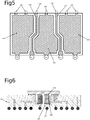
- the capacitor layers are perpendicular to the silicon chip die surface. So current can flow from the substrate (supply side) through the capacitor plates of one pole to the silicon chip (load side). And the return current can flow in opposite direction through the capacitor plates of the other pole. This connection is a substitute for the power network that the capacitor blocks in the substrate routing space.
- the capacitor may have a layer that includes signal wires. These wires are metal shapes on some of the metal layer of the capacitor and is isolated from both poles. They connect a dedicated signal terminal on silicon chip facing side and a dedicated signal terminal on the substrate facing side. These connections can substitute blocked routing space for data signals and differential signal pairs.
- An embodiment of the multi-layer ceramic capacitor can be made by printing different type of metallic layers on dielectric sheets:
- the base shape of the positive pole layer is rectangular, with clearance to all borders. But on the sides where the positive terminals will be added, there is no clearance and metal layer extends to the border.
- the base shape of the negative pole layer is rectangular, with clearance to all borders. But on the sides where the negative terminals will be added, there is no clearance and metal layer extends to the border. If there are signal terminals the shape of a layer contains signal traces between signal pins on two sides. The signal traces have clearance to the poles and other signal traces.
- the finished multi-layer ceramic capacitor then embedded into the substrate by the following steps.
- Some layers of the substrate have holes that form a cavity.
- the size of the cavity is chosen large enough for one or more capacitors. If the capacitor is an embodiment of the invention without solder balls then solder paste is applied to the solder pads at the substrate inside the cavity.
- the capacitors are placed inside the cavities of the substrate. Heating up the assembly for a thermal reflow process of the solder. Remaining gaps between capacitor and substrate can be filled with an underfill adhesive.
- the surface of the assembly can be polished to levelize the capacitor pins and the substrate surface. An additional substrate layer can be applied.
- the plating of the silicon chip facing side of the decoupling capacitor can also be deferred after embedding it into the substrate and be applied in the same plating process together with a substrate layer metal plating or the via metal plating.
- the silicon chip with solder balls is attached to the substrate with the embedded capacitors in a flip chip process.
- a thermal reflow of the solder balls make a permanent electrical joint between the silicon chip and pads of both the capacitor and the substrate.
Landscapes
- Engineering & Computer Science (AREA)
- Power Engineering (AREA)
- Manufacturing & Machinery (AREA)
- Microelectronics & Electronic Packaging (AREA)
- Structures For Mounting Electric Components On Printed Circuit Boards (AREA)
- Fixed Capacitors And Capacitor Manufacturing Machines (AREA)
Priority Applications (1)
| Application Number | Priority Date | Filing Date | Title |
|---|---|---|---|
| EP19176847.2A EP3745456A1 (fr) | 2019-05-27 | 2019-05-27 | Couches de condensateur de découplage montées perpendiculairement entre une puce à semi-conducteur et un substrat |
Applications Claiming Priority (1)
| Application Number | Priority Date | Filing Date | Title |
|---|---|---|---|
| EP19176847.2A EP3745456A1 (fr) | 2019-05-27 | 2019-05-27 | Couches de condensateur de découplage montées perpendiculairement entre une puce à semi-conducteur et un substrat |
Publications (1)
| Publication Number | Publication Date |
|---|---|
| EP3745456A1 true EP3745456A1 (fr) | 2020-12-02 |
Family
ID=66668748
Family Applications (1)
| Application Number | Title | Priority Date | Filing Date |
|---|---|---|---|
| EP19176847.2A Withdrawn EP3745456A1 (fr) | 2019-05-27 | 2019-05-27 | Couches de condensateur de découplage montées perpendiculairement entre une puce à semi-conducteur et un substrat |
Country Status (1)
| Country | Link |
|---|---|
| EP (1) | EP3745456A1 (fr) |
Citations (6)
| Publication number | Priority date | Publication date | Assignee | Title |
|---|---|---|---|---|
| US6292351B1 (en) * | 1999-11-17 | 2001-09-18 | Tdk Corporation | Multilayer ceramic capacitor for three-dimensional mounting |
| US20030161086A1 (en) * | 2000-07-18 | 2003-08-28 | X2Y Attenuators, Llc | Paired multi-layered dielectric independent passive component architecture resulting in differential and common mode filtering with surge protection in one integrated package |
| US20080180878A1 (en) * | 2007-01-31 | 2008-07-31 | Advanced Semiconductor Engineering, Inc. | Package structure with embedded capacitor, fabricating process thereof and applications of the same |
| US20100300740A1 (en) * | 2009-06-01 | 2010-12-02 | Seiji Ichiyanagi | Ceramic Capacitor and Wiring Board |
| US20160055976A1 (en) * | 2014-08-25 | 2016-02-25 | Qualcomm Incorporated | Package substrates including embedded capacitors |
| US20170207024A1 (en) * | 2016-01-18 | 2017-07-20 | Apple Inc. | Multi-layer ceramic capacitors with bottom or side terminations |
-
2019
- 2019-05-27 EP EP19176847.2A patent/EP3745456A1/fr not_active Withdrawn
Patent Citations (6)
| Publication number | Priority date | Publication date | Assignee | Title |
|---|---|---|---|---|
| US6292351B1 (en) * | 1999-11-17 | 2001-09-18 | Tdk Corporation | Multilayer ceramic capacitor for three-dimensional mounting |
| US20030161086A1 (en) * | 2000-07-18 | 2003-08-28 | X2Y Attenuators, Llc | Paired multi-layered dielectric independent passive component architecture resulting in differential and common mode filtering with surge protection in one integrated package |
| US20080180878A1 (en) * | 2007-01-31 | 2008-07-31 | Advanced Semiconductor Engineering, Inc. | Package structure with embedded capacitor, fabricating process thereof and applications of the same |
| US20100300740A1 (en) * | 2009-06-01 | 2010-12-02 | Seiji Ichiyanagi | Ceramic Capacitor and Wiring Board |
| US20160055976A1 (en) * | 2014-08-25 | 2016-02-25 | Qualcomm Incorporated | Package substrates including embedded capacitors |
| US20170207024A1 (en) * | 2016-01-18 | 2017-07-20 | Apple Inc. | Multi-layer ceramic capacitors with bottom or side terminations |
Similar Documents
| Publication | Publication Date | Title |
|---|---|---|
| US6740964B2 (en) | Semiconductor package for three-dimensional mounting, fabrication method thereof, and semiconductor device | |
| JP4606849B2 (ja) | デカップリングコンデンサを有する半導体チップパッケージ及びその製造方法 | |
| US11031371B2 (en) | Semiconductor package and method of fabricating semiconductor package | |
| CN100350602C (zh) | 带内插器的微电子电路封装 | |
| US7889509B2 (en) | Ceramic capacitor | |
| US5475264A (en) | Arrangement having multilevel wiring structure used for electronic component module | |
| US6680218B2 (en) | Fabrication method for vertical electronic circuit package and system | |
| US9839132B2 (en) | Component-embedded substrate | |
| US8791501B1 (en) | Integrated passive device structure and method | |
| US12288756B2 (en) | Semiconductor package with integrated capacitors | |
| US10790225B1 (en) | Chip package structure and chip package method including bare chips with capacitor polar plate | |
| US20200279804A1 (en) | Wiring structure and method for manufacturing the same | |
| US12136613B2 (en) | Chip package with near-die integrated passive device | |
| JP3899059B2 (ja) | 低抵抗高密度信号線をする電子パッケージおよびその製造方法 | |
| US20160284663A1 (en) | Chip package assembly and manufacturing method thereof | |
| WO2003034491A2 (fr) | Composant a semi-conducteur | |
| US9629249B2 (en) | Component-embedded substrate and communication module | |
| KR101134519B1 (ko) | 매립형 인쇄회로기판 및 그 제조방법 | |
| EP2849226B1 (fr) | Boitier pour semi-conducteur | |
| US6888218B2 (en) | Embedded capacitor multi-chip modules | |
| US8324727B2 (en) | Low profile discrete electronic components and applications of same | |
| CN119542260A (zh) | 一种埋入式封装结构、电源装置及电子设备 | |
| US20240363503A1 (en) | Semiconductor devices with double-sided fanout chip packages | |
| RU2653183C1 (ru) | Многокристальная микросхема | |
| US20260068713A1 (en) | Semiconductor package and manufacturing method of the same |
Legal Events
| Date | Code | Title | Description |
|---|---|---|---|
| PUAI | Public reference made under article 153(3) epc to a published international application that has entered the european phase |
Free format text: ORIGINAL CODE: 0009012 |
|
| STAA | Information on the status of an ep patent application or granted ep patent |
Free format text: STATUS: THE APPLICATION HAS BEEN PUBLISHED |
|
| AK | Designated contracting states |
Kind code of ref document: A1 Designated state(s): AL AT BE BG CH CY CZ DE DK EE ES FI FR GB GR HR HU IE IS IT LI LT LU LV MC MK MT NL NO PL PT RO RS SE SI SK SM TR |
|
| AX | Request for extension of the european patent |
Extension state: BA ME |
|
| STAA | Information on the status of an ep patent application or granted ep patent |
Free format text: STATUS: REQUEST FOR EXAMINATION WAS MADE |
|
| 17P | Request for examination filed |
Effective date: 20201213 |
|
| RBV | Designated contracting states (corrected) |
Designated state(s): AL AT BE BG CH CY CZ DE DK EE ES FI FR GB GR HR HU IE IS IT LI LT LU LV MC MK MT NL NO PL PT RO RS SE SI SK SM TR |
|
| STAA | Information on the status of an ep patent application or granted ep patent |
Free format text: STATUS: EXAMINATION IS IN PROGRESS |
|
| STAA | Information on the status of an ep patent application or granted ep patent |
Free format text: STATUS: THE APPLICATION HAS BEEN WITHDRAWN |
|
| 17Q | First examination report despatched |
Effective date: 20220222 |
|
| 18W | Application withdrawn |
Effective date: 20220228 |