EP3745471A1 - Verfahren zur laserbehandlung eines halbleiterwafers mit algainp-leds zur erhöhung ihrer lichterzeugungseffizienz - Google Patents
Verfahren zur laserbehandlung eines halbleiterwafers mit algainp-leds zur erhöhung ihrer lichterzeugungseffizienz Download PDFInfo
- Publication number
- EP3745471A1 EP3745471A1 EP19177581.6A EP19177581A EP3745471A1 EP 3745471 A1 EP3745471 A1 EP 3745471A1 EP 19177581 A EP19177581 A EP 19177581A EP 3745471 A1 EP3745471 A1 EP 3745471A1
- Authority
- EP
- European Patent Office
- Prior art keywords
- laser beam
- algainp
- led
- active layer
- light generating
- Prior art date
- Legal status (The legal status is an assumption and is not a legal conclusion. Google has not performed a legal analysis and makes no representation as to the accuracy of the status listed.)
- Pending
Links
Images

Classifications
-
- H—ELECTRICITY
- H10—SEMICONDUCTOR DEVICES; ELECTRIC SOLID-STATE DEVICES NOT OTHERWISE PROVIDED FOR
- H10H—INORGANIC LIGHT-EMITTING SEMICONDUCTOR DEVICES HAVING POTENTIAL BARRIERS
- H10H20/00—Individual inorganic light-emitting semiconductor devices having potential barriers, e.g. light-emitting diodes [LED]
- H10H20/01—Manufacture or treatment
-
- H—ELECTRICITY
- H10—SEMICONDUCTOR DEVICES; ELECTRIC SOLID-STATE DEVICES NOT OTHERWISE PROVIDED FOR
- H10P—GENERIC PROCESSES OR APPARATUS FOR THE MANUFACTURE OR TREATMENT OF DEVICES COVERED BY CLASS H10
- H10P34/00—Irradiation with electromagnetic or particle radiation of wafers, substrates or parts of devices
- H10P34/40—Irradiation with electromagnetic or particle radiation of wafers, substrates or parts of devices with high-energy radiation
- H10P34/42—Irradiation with electromagnetic or particle radiation of wafers, substrates or parts of devices with high-energy radiation with electromagnetic radiation, e.g. laser annealing
-
- H—ELECTRICITY
- H10—SEMICONDUCTOR DEVICES; ELECTRIC SOLID-STATE DEVICES NOT OTHERWISE PROVIDED FOR
- H10H—INORGANIC LIGHT-EMITTING SEMICONDUCTOR DEVICES HAVING POTENTIAL BARRIERS
- H10H20/00—Individual inorganic light-emitting semiconductor devices having potential barriers, e.g. light-emitting diodes [LED]
- H10H20/01—Manufacture or treatment
- H10H20/011—Manufacture or treatment of bodies, e.g. forming semiconductor layers
- H10H20/013—Manufacture or treatment of bodies, e.g. forming semiconductor layers having light-emitting regions comprising only Group III-V materials
-
- H—ELECTRICITY
- H10—SEMICONDUCTOR DEVICES; ELECTRIC SOLID-STATE DEVICES NOT OTHERWISE PROVIDED FOR
- H10P—GENERIC PROCESSES OR APPARATUS FOR THE MANUFACTURE OR TREATMENT OF DEVICES COVERED BY CLASS H10
- H10P14/00—Formation of materials, e.g. in the shape of layers or pillars
- H10P14/20—Formation of materials, e.g. in the shape of layers or pillars of semiconductor materials
- H10P14/38—Formation of materials, e.g. in the shape of layers or pillars of semiconductor materials characterised by treatments done after the formation of the materials
- H10P14/3824—Intermixing, interdiffusion or disordering of III-V heterostructures, e.g. IILD
-
- H—ELECTRICITY
- H10—SEMICONDUCTOR DEVICES; ELECTRIC SOLID-STATE DEVICES NOT OTHERWISE PROVIDED FOR
- H10H—INORGANIC LIGHT-EMITTING SEMICONDUCTOR DEVICES HAVING POTENTIAL BARRIERS
- H10H20/00—Individual inorganic light-emitting semiconductor devices having potential barriers, e.g. light-emitting diodes [LED]
- H10H20/80—Constructional details
- H10H20/81—Bodies
- H10H20/811—Bodies having quantum effect structures or superlattices, e.g. tunnel junctions
- H10H20/812—Bodies having quantum effect structures or superlattices, e.g. tunnel junctions within the light-emitting regions, e.g. having quantum confinement structures
Definitions
- the present invention generally relates to the field of manufacturing of light-emitting diode chips.
- the present invention relates to increasing the light generating efficiency of aluminum gallium indium phosphide LEDs.
- AlGaInP aluminum gallium indium phosphide
- Zinc diffusion leads to so-called quantum well intermixing, meaning that the bandgap of the optically active material in the LED's mesa edge is increased. This in turn means that less electron-hole pairs can reach the mesa edge. Accordingly, the electron-hole pairs are confined to the LED's center and can recombine optically to generate light.
- this problem is solved by a method of treating a semiconductor wafer comprising a set of Aluminum Gallium Indium Phosphide light emitting diodes or AlGaInP-LEDs to increase the light generating efficiency of the AlGaInP-LEDs, wherein each ALGaInP-LED includes a core active layer for light generation sandwiched between two outer layers, the core active layer having a central light generating area and a peripheral edge surrounding the central light generating area, the method comprising the step of treating the peripheral edge of the core active layer of each AlGaInP-LED with a laser beam, thus increasing the minimum band gap in each peripheral edge to such an extent that, during later operation of the AlGaInP-LED, the electron-hole recombination is essentially confined to the central light generating area.
- the laser beam treatment may involve scanning the wafer with the laser beam according to a predefined pattern.
- the photon energy of the laser beam may be higher than the minimum band gap of the core active layer and lower than the band gaps of the two outer layers such that, during the laser beam treatment, the laser beam energy is primarily transferred to the core active layer's peripheral edge.
- Each AlGaInP-LED may be a red light LED.
- the wavelength of the laser beam may in particular be in the range of 550 to 640 nm.
- the laser beam may have a Gaussian shape/profile.
- the laser beam may be generated by a pulsed laser.
- the wafer Prior to the laser beam treatment, the wafer may be heated to a background temperature to reduce the power requirements of the laser beam treatment.
- the laser beam power density may be between 0.1 and 100 mJ/mm2, and preferably between 1 and 10 mJ/ mm2.
- the wafer may be etched, thus obtaining, for each AlGaInP-LED, a chip preform, wherein, preferably, after the etching, the wafer is diced into individual AlGaInP-LED chips, e.g. by laser cutting.
- the duration of the laser beam treatment may be between 1s and 10min and preferably between 10s and 2min.
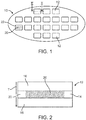
- a semiconductor wafer 10 comprising a set of aluminum gallium indium phosphide light-emitting diodes (AlGaInP-LEDs) 12.
- AlGaInP-LEDs aluminum gallium indium phosphide light-emitting diodes
- Each LED is a PN junction, which has been formed in the wafer 10 according to well-known methods.
- FIG. 2 is a cross section of one of the LEDs 12.
- Each LED 12 includes a core active layer 14 for light generation sandwiched between two outer layers 16 and 18.
- the core active layer 14 has a central light generating area 20. This area 20 is identified by the dotted region.
- the central light generating area 20 is surrounded by a peripheral edge 22.
- the bandgap diagram in Figure 4 shows the bandgap as a function of the depth T into the LED 12, see Figure 2 .
- the upper outer layer 16 of the LED 12 is a P-doped layer.
- the bandgap shape of this P-type doped layer 16 is a P-ramp 24, followed by a P-setback 26.
- the bandgap of the P-setback 26 is denoted by BG1.
- the bandgap shape of the active layer 14 is, along the depth T, a series of quantum wells Q separated by barriers B. In the example shown in Figure 4 , active layer 14 has two quantum wells Q separated by one barrier B.
- the quantum wells Q define a bandgap BG2, which is smaller than the bandgap BG1.
- the bandgap of the quantum wells Q is the minimum bandgap of the core active layer 14.
- the lower outer layer 18 has a bandgap shape comparable to the one of the upper outer layer 16, with a setback 28, and ramp 30. However, the lower outer layer 18 is N-type doped.
- individual LED chips 38 with increased light generating efficiency are obtained from the wafer 10 as follows: In a first step a), a hatched zone Z of the wafer 10 is treated with a laser beam L, as depicted in the small process drawing located right to the flow diagram's first arrow 100.
- the laser beam treatment involves scanning wafer 10 according to a predefined pattern. More precisely, the laser beam L scans the surface of the wafer 10, which is not taken up by the LEDs 12, and, on top of that, the peripheral edges 22 of the core active layers 14 of the LEDs 12. Different scanning patterns are possible, as long as the pattern involves the scanning of the peripheral edges 22 of the core active layers 14 of the LEDs 12.
- the photon energy of the laser beam L is higher than the minimum bandgap BG2 of the core active layer 14 and lower than the bandgap BG1 of the two outer layers 16 and 18. Hence, during the laser beam treatment, the laser beam energy is primarily transferred to the core active layer's peripheral edge 22.
- the laser beam's wavelength is chosen in particular such that only the quantum wells Q, the barriers Band the setbacks 26, 28 are optically stimulated, as illustrated by the arrows E in Figure 4 .
- the wavelength of the laser beam may be chosen anywhere within the range of 550 to 640 nm.
- the shape or profile of the laser beam may in particular correspond to a Gaussian profile.
- the laser beam may be a pulsed laser, such as a nano- pico- or femtosecond laser.
- the power density of the laser beam may be between 0.1 and 100 mJ per mm 2 , and preferably between 1 and 10 mJ per mm 2 .
- the overall duration of the wafer's laser beam treatment may be between 1 second and 10 minutes, and preferably between 10 seconds and 2 minutes.
- the effect of the laser beam treatment on the bandgap structure is shown on the right hand side of Figure 4 . It is apparent that the laser beam L, by locally heating the treated area, effectively destroys the quantum wells Q. Hence, after the laser beam treatment, the peripheral edges 22 no longer have any core active layer 14.
- the laser beam treatment results in a mixing of the quantum well material with the barrier material (so-called quantum well intermixing), which increases the bandgap.
- the semiconductor wafer 10 may be etched (so-called "Mesa etching"), thus obtaining for each LED 12, a chip preform 32.
- the etching step 102 is identified by the letter b) in Figure 3 .
- the etched parts of the wafer 10 are highlighted by a crosshatch pattern Y.
- Each chip preform 32 has a central zone 34 and a peripheral boundary 36.
- the peripheral boundary 36 has been laser treated and thus lacks any core active layer 14.
- the central zone 34 still has a core active layer 14.
- wafer 10 is diced, e.g. by laser cutting, as shown in step 104 of Figure 3 .
- the laser treatment step 100 may optionally be preceded by a step of heating the semiconductor wafer 10 to a background temperature to reduce the power requirements of the laser beam treatment.
- the electron-hole recombination is essentially confined to the central light generating area 20. This is because of the increased bandgap in the peripheral edges 22, which prevents electron-hole pairs from entering the same.
- the laser treatment method of the present disclosure is especially useful for very small red LEDs, which are e.g. used as part of high resolution monitors and displays.
Landscapes
- Led Devices (AREA)
Priority Applications (4)
| Application Number | Priority Date | Filing Date | Title |
|---|---|---|---|
| EP19177581.6A EP3745471A1 (de) | 2019-05-31 | 2019-05-31 | Verfahren zur laserbehandlung eines halbleiterwafers mit algainp-leds zur erhöhung ihrer lichterzeugungseffizienz |
| CN202080041359.7A CN113994483A (zh) | 2019-05-31 | 2020-05-19 | 对包括algainp-led的半导体晶圆进行激光处理以提高其光产生效率的方法 |
| US17/615,487 US12426404B2 (en) | 2019-05-31 | 2020-05-19 | Method of laser treatment of a semiconductor wafer comprising AlGaInP-LEDs to increase their light generating efficiency |
| PCT/EP2020/063906 WO2020239526A1 (en) | 2019-05-31 | 2020-05-19 | Method of laser treatment of a semiconductor wafer comprising algainp-leds to increase their light generating efficiency |
Applications Claiming Priority (1)
| Application Number | Priority Date | Filing Date | Title |
|---|---|---|---|
| EP19177581.6A EP3745471A1 (de) | 2019-05-31 | 2019-05-31 | Verfahren zur laserbehandlung eines halbleiterwafers mit algainp-leds zur erhöhung ihrer lichterzeugungseffizienz |
Publications (1)
| Publication Number | Publication Date |
|---|---|
| EP3745471A1 true EP3745471A1 (de) | 2020-12-02 |
Family
ID=66685397
Family Applications (1)
| Application Number | Title | Priority Date | Filing Date |
|---|---|---|---|
| EP19177581.6A Pending EP3745471A1 (de) | 2019-05-31 | 2019-05-31 | Verfahren zur laserbehandlung eines halbleiterwafers mit algainp-leds zur erhöhung ihrer lichterzeugungseffizienz |
Country Status (4)
| Country | Link |
|---|---|
| US (1) | US12426404B2 (de) |
| EP (1) | EP3745471A1 (de) |
| CN (1) | CN113994483A (de) |
| WO (1) | WO2020239526A1 (de) |
Families Citing this family (1)
| Publication number | Priority date | Publication date | Assignee | Title |
|---|---|---|---|---|
| DE102021104685A1 (de) | 2021-02-26 | 2022-09-01 | OSRAM Opto Semiconductors Gesellschaft mit beschränkter Haftung | Verfahren zur herstellung eines optoelektronischen halbleiterbauelements und optoelektronisches halbleiterbauelement |
Citations (5)
| Publication number | Priority date | Publication date | Assignee | Title |
|---|---|---|---|---|
| US4731338A (en) * | 1986-10-09 | 1988-03-15 | Amoco Corporation | Method for selective intermixing of layered structures composed of thin solid films |
| US20020003918A1 (en) * | 2000-03-08 | 2002-01-10 | Ooi Boon Siew | Quantum well intermixing |
| WO2003038487A2 (en) * | 2001-10-31 | 2003-05-08 | The University Court Of The University Of Glasgow | Improvements in and relating to optoelectronic devices |
| WO2004095662A2 (en) * | 2003-04-23 | 2004-11-04 | Denselight Semiconductors Pte Ltd | Bandgap engineering |
| US20170170360A1 (en) * | 2015-01-06 | 2017-06-15 | Apple Inc. | Led structures for reduced non-radiative sidewall recombination |
Family Cites Families (7)
| Publication number | Priority date | Publication date | Assignee | Title |
|---|---|---|---|---|
| US4771010A (en) * | 1986-11-21 | 1988-09-13 | Xerox Corporation | Energy beam induced layer disordering (EBILD) |
| JP3681535B2 (ja) | 1998-03-13 | 2005-08-10 | 日本オプネクスト株式会社 | 光半導体素子の製造方法 |
| WO2008028130A1 (en) * | 2006-09-01 | 2008-03-06 | William Marsh Rice University | Compositions for surface enhanced infrared absorption spectra and methods of using same |
| KR102334468B1 (ko) * | 2009-10-30 | 2021-12-06 | 가부시키가이샤 한도오따이 에네루기 켄큐쇼 | 반도체 장치 |
| US9460966B2 (en) * | 2013-10-10 | 2016-10-04 | Applied Materials, Inc. | Method and apparatus for dicing wafers having thick passivation polymer layer |
| US9687936B2 (en) * | 2013-12-17 | 2017-06-27 | Corning Incorporated | Transparent material cutting with ultrafast laser and beam optics |
| CN108878612A (zh) | 2018-06-25 | 2018-11-23 | 山东浪潮华光光电子股份有限公司 | 一种提高AlGaInP LED侧面出光的管芯结构 |
-
2019
- 2019-05-31 EP EP19177581.6A patent/EP3745471A1/de active Pending
-
2020
- 2020-05-19 WO PCT/EP2020/063906 patent/WO2020239526A1/en not_active Ceased
- 2020-05-19 US US17/615,487 patent/US12426404B2/en active Active
- 2020-05-19 CN CN202080041359.7A patent/CN113994483A/zh active Pending
Patent Citations (5)
| Publication number | Priority date | Publication date | Assignee | Title |
|---|---|---|---|---|
| US4731338A (en) * | 1986-10-09 | 1988-03-15 | Amoco Corporation | Method for selective intermixing of layered structures composed of thin solid films |
| US20020003918A1 (en) * | 2000-03-08 | 2002-01-10 | Ooi Boon Siew | Quantum well intermixing |
| WO2003038487A2 (en) * | 2001-10-31 | 2003-05-08 | The University Court Of The University Of Glasgow | Improvements in and relating to optoelectronic devices |
| WO2004095662A2 (en) * | 2003-04-23 | 2004-11-04 | Denselight Semiconductors Pte Ltd | Bandgap engineering |
| US20170170360A1 (en) * | 2015-01-06 | 2017-06-15 | Apple Inc. | Led structures for reduced non-radiative sidewall recombination |
Also Published As
| Publication number | Publication date |
|---|---|
| WO2020239526A1 (en) | 2020-12-03 |
| US12426404B2 (en) | 2025-09-23 |
| CN113994483A (zh) | 2022-01-28 |
| US20220238752A1 (en) | 2022-07-28 |
Similar Documents
| Publication | Publication Date | Title |
|---|---|---|
| KR101632768B1 (ko) | 성장 기판을 제거한 직렬 연결 플립칩 led | |
| JP6260601B2 (ja) | 半導体素子の製造方法 | |
| JP5956209B2 (ja) | 金属−炭化珪素オーミックコンタクトの局所的アニーリングおよびそのようにして形成された素子 | |
| US20100006864A1 (en) | Implanted connectors in led submount for pec etching bias | |
| TW201203603A (en) | Bond pad isolation and current confinement in an LED using ion implantation | |
| US20120319149A1 (en) | Light-Emitting Device Structure and Method for Manufacturing the Same | |
| US5994720A (en) | Indirect bandgap semiconductor optoelectronic device | |
| JP5420550B2 (ja) | キャリア注入を用いるシリコン発光素子 | |
| US20130026447A1 (en) | Surface-Emitting Semiconductor Light-Emitting Diode | |
| US12426404B2 (en) | Method of laser treatment of a semiconductor wafer comprising AlGaInP-LEDs to increase their light generating efficiency | |
| JP5998243B2 (ja) | パターン効果を低減したGaNLEDのレーザーアニール | |
| KR20120100193A (ko) | 발광 다이오드 칩 | |
| WO2020119049A1 (zh) | 一种激光剥离方法及系统 | |
| JP2014517543A (ja) | 半導体発光素子及びその製造方法 | |
| CN106981553B (zh) | 发光元件及其制造方法 | |
| CN113544862A (zh) | 光电子半导体芯片和用于制造光电子半导体芯片的方法 | |
| TWI453953B (zh) | 氮化鎵發光二極體及其形成方法 | |
| KR20230117603A (ko) | 광전자 반도체 컴포넌트 및 광전자 반도체 컴포넌트를제조하기 위한 방법 | |
| JP2013048236A (ja) | GaNLED用高速熱アニール | |
| KR100900114B1 (ko) | 반도체 층 내부에 전기 전도도가 감소하는 영역을 형성하기위한 방법 및 광전 반도체 소자 | |
| US11955588B2 (en) | Optoelectronic semiconductor component and method for producing an optoelectronic semiconductor component | |
| CN102861994A (zh) | 一种发光原件的切割方法 | |
| JP5940315B2 (ja) | 半導体発光素子及びその製造方法 | |
| JP2000357818A (ja) | 発光素子およびその製造方法 | |
| CN115799054B (zh) | 一种激光掺杂方法、太阳能电池制作方法、基材及电池 |
Legal Events
| Date | Code | Title | Description |
|---|---|---|---|
| PUAI | Public reference made under article 153(3) epc to a published international application that has entered the european phase |
Free format text: ORIGINAL CODE: 0009012 |
|
| STAA | Information on the status of an ep patent application or granted ep patent |
Free format text: STATUS: THE APPLICATION HAS BEEN PUBLISHED |
|
| AK | Designated contracting states |
Kind code of ref document: A1 Designated state(s): AL AT BE BG CH CY CZ DE DK EE ES FI FR GB GR HR HU IE IS IT LI LT LU LV MC MK MT NL NO PL PT RO RS SE SI SK SM TR |
|
| AX | Request for extension of the european patent |
Extension state: BA ME |
|
| STAA | Information on the status of an ep patent application or granted ep patent |
Free format text: STATUS: REQUEST FOR EXAMINATION WAS MADE |
|
| 17P | Request for examination filed |
Effective date: 20210602 |
|
| RBV | Designated contracting states (corrected) |
Designated state(s): AL AT BE BG CH CY CZ DE DK EE ES FI FR GB GR HR HU IE IS IT LI LT LU LV MC MK MT NL NO PL PT RO RS SE SI SK SM TR |
|
| P01 | Opt-out of the competence of the unified patent court (upc) registered |
Effective date: 20230613 |
|
| STAA | Information on the status of an ep patent application or granted ep patent |
Free format text: STATUS: EXAMINATION IS IN PROGRESS |
|
| 17Q | First examination report despatched |
Effective date: 20241213 |