EP3745527B1 - Flüssigkristallphasenschieber, flüssigkristallantenne und herstellungsverfahren für einen flüssigkristallphasenschieber - Google Patents
Flüssigkristallphasenschieber, flüssigkristallantenne und herstellungsverfahren für einen flüssigkristallphasenschieber Download PDFInfo
- Publication number
- EP3745527B1 EP3745527B1 EP19863992.4A EP19863992A EP3745527B1 EP 3745527 B1 EP3745527 B1 EP 3745527B1 EP 19863992 A EP19863992 A EP 19863992A EP 3745527 B1 EP3745527 B1 EP 3745527B1
- Authority
- EP
- European Patent Office
- Prior art keywords
- substrate
- alignment mark
- metal film
- liquid crystal
- layer
- Prior art date
- Legal status (The legal status is an assumption and is not a legal conclusion. Google has not performed a legal analysis and makes no representation as to the accuracy of the status listed.)
- Active
Links
Images

Classifications
-
- H—ELECTRICITY
- H01—ELECTRIC ELEMENTS
- H01Q—ANTENNAS, i.e. RADIO AERIALS
- H01Q3/00—Arrangements for changing or varying the orientation or the shape of the directional pattern of the waves radiated from an antenna or antenna system
- H01Q3/26—Arrangements for changing or varying the orientation or the shape of the directional pattern of the waves radiated from an antenna or antenna system varying the relative phase or relative amplitude of energisation between two or more active radiating elements; varying the distribution of energy across a radiating aperture
- H01Q3/30—Arrangements for changing or varying the orientation or the shape of the directional pattern of the waves radiated from an antenna or antenna system varying the relative phase or relative amplitude of energisation between two or more active radiating elements; varying the distribution of energy across a radiating aperture varying the relative phase between the radiating elements of an array
- H01Q3/34—Arrangements for changing or varying the orientation or the shape of the directional pattern of the waves radiated from an antenna or antenna system varying the relative phase or relative amplitude of energisation between two or more active radiating elements; varying the distribution of energy across a radiating aperture varying the relative phase between the radiating elements of an array by electrical means
- H01Q3/36—Arrangements for changing or varying the orientation or the shape of the directional pattern of the waves radiated from an antenna or antenna system varying the relative phase or relative amplitude of energisation between two or more active radiating elements; varying the distribution of energy across a radiating aperture varying the relative phase between the radiating elements of an array by electrical means with variable phase-shifters
-
- G—PHYSICS
- G02—OPTICS
- G02F—OPTICAL DEVICES OR ARRANGEMENTS FOR THE CONTROL OF LIGHT BY MODIFICATION OF THE OPTICAL PROPERTIES OF THE MEDIA OF THE ELEMENTS INVOLVED THEREIN; NON-LINEAR OPTICS; FREQUENCY-CHANGING OF LIGHT; OPTICAL LOGIC ELEMENTS; OPTICAL ANALOGUE/DIGITAL CONVERTERS
- G02F1/00—Devices or arrangements for the control of the intensity, colour, phase, polarisation or direction of light arriving from an independent light source, e.g. switching, gating or modulating; Non-linear optics
- G02F1/01—Devices or arrangements for the control of the intensity, colour, phase, polarisation or direction of light arriving from an independent light source, e.g. switching, gating or modulating; Non-linear optics for the control of the intensity, phase, polarisation or colour
- G02F1/13—Devices or arrangements for the control of the intensity, colour, phase, polarisation or direction of light arriving from an independent light source, e.g. switching, gating or modulating; Non-linear optics for the control of the intensity, phase, polarisation or colour based on liquid crystals, e.g. single liquid crystal display cells
- G02F1/133—Constructional arrangements; Operation of liquid crystal cells; Circuit arrangements
- G02F1/1333—Constructional arrangements; Manufacturing methods
-
- H—ELECTRICITY
- H01—ELECTRIC ELEMENTS
- H01P—WAVEGUIDES; RESONATORS, LINES, OR OTHER DEVICES OF THE WAVEGUIDE TYPE
- H01P1/00—Auxiliary devices
- H01P1/18—Phase-shifters
-
- G—PHYSICS
- G02—OPTICS
- G02F—OPTICAL DEVICES OR ARRANGEMENTS FOR THE CONTROL OF LIGHT BY MODIFICATION OF THE OPTICAL PROPERTIES OF THE MEDIA OF THE ELEMENTS INVOLVED THEREIN; NON-LINEAR OPTICS; FREQUENCY-CHANGING OF LIGHT; OPTICAL LOGIC ELEMENTS; OPTICAL ANALOGUE/DIGITAL CONVERTERS
- G02F1/00—Devices or arrangements for the control of the intensity, colour, phase, polarisation or direction of light arriving from an independent light source, e.g. switching, gating or modulating; Non-linear optics
- G02F1/01—Devices or arrangements for the control of the intensity, colour, phase, polarisation or direction of light arriving from an independent light source, e.g. switching, gating or modulating; Non-linear optics for the control of the intensity, phase, polarisation or colour
- G02F1/13—Devices or arrangements for the control of the intensity, colour, phase, polarisation or direction of light arriving from an independent light source, e.g. switching, gating or modulating; Non-linear optics for the control of the intensity, phase, polarisation or colour based on liquid crystals, e.g. single liquid crystal display cells
- G02F1/1303—Apparatus specially adapted to the manufacture of LCDs
-
- G—PHYSICS
- G02—OPTICS
- G02F—OPTICAL DEVICES OR ARRANGEMENTS FOR THE CONTROL OF LIGHT BY MODIFICATION OF THE OPTICAL PROPERTIES OF THE MEDIA OF THE ELEMENTS INVOLVED THEREIN; NON-LINEAR OPTICS; FREQUENCY-CHANGING OF LIGHT; OPTICAL LOGIC ELEMENTS; OPTICAL ANALOGUE/DIGITAL CONVERTERS
- G02F1/00—Devices or arrangements for the control of the intensity, colour, phase, polarisation or direction of light arriving from an independent light source, e.g. switching, gating or modulating; Non-linear optics
- G02F1/01—Devices or arrangements for the control of the intensity, colour, phase, polarisation or direction of light arriving from an independent light source, e.g. switching, gating or modulating; Non-linear optics for the control of the intensity, phase, polarisation or colour
- G02F1/13—Devices or arrangements for the control of the intensity, colour, phase, polarisation or direction of light arriving from an independent light source, e.g. switching, gating or modulating; Non-linear optics for the control of the intensity, phase, polarisation or colour based on liquid crystals, e.g. single liquid crystal display cells
- G02F1/1313—Devices or arrangements for the control of the intensity, colour, phase, polarisation or direction of light arriving from an independent light source, e.g. switching, gating or modulating; Non-linear optics for the control of the intensity, phase, polarisation or colour based on liquid crystals, e.g. single liquid crystal display cells specially adapted for a particular application
-
- H—ELECTRICITY
- H01—ELECTRIC ELEMENTS
- H01P—WAVEGUIDES; RESONATORS, LINES, OR OTHER DEVICES OF THE WAVEGUIDE TYPE
- H01P1/00—Auxiliary devices
- H01P1/18—Phase-shifters
- H01P1/184—Strip line phase-shifters
-
- H—ELECTRICITY
- H01—ELECTRIC ELEMENTS
- H01P—WAVEGUIDES; RESONATORS, LINES, OR OTHER DEVICES OF THE WAVEGUIDE TYPE
- H01P11/00—Apparatus or processes specially adapted for manufacturing waveguides or resonators, lines, or other devices of the waveguide type
-
- H—ELECTRICITY
- H01—ELECTRIC ELEMENTS
- H01Q—ANTENNAS, i.e. RADIO AERIALS
- H01Q1/00—Details of, or arrangements associated with, antennas
- H01Q1/36—Structural form of radiating elements, e.g. cone, spiral, umbrella; Particular materials used therewith
- H01Q1/38—Structural form of radiating elements, e.g. cone, spiral, umbrella; Particular materials used therewith formed by a conductive layer on an insulating support
Definitions
- the present disclosure relates to the technical field of wireless communications, and more particularly relates to a liquid crystal phase shifter, a liquid crystal antenna and a manufacturing method of the liquid crystal phase shifter.
- Hotspot technologies include 5G and satellite mobile Internet communication technologies.
- an antenna As a core device for sending and receiving communication information, an antenna has become a key factor that affects performance indexes of an information network and user application effects.
- a liquid crystal phase shifter is a key component of the liquid crystal antenna. How to design and manufacture a liquid crystal phase shifter and a liquid crystal antenna suitable for the spectrums above the ultra-high frequency bands is a problem to be solved by those skilled in the art.
- Patent document CN 108 493 592A describes a microstrip antenna, a preparation method thereof and electronic equipment.
- Patent document US 2018/159239 A1 describes an electro-magnetic transmission line system having very low loss, which includes a low dielectric material proximate to a conductor on one side, a conductor on the opposite side and a substrate to which at least one of the conductors are attached.
- Patent document US 6 681 005 B2 describes an apparatus for manufacturing a liquid crystal display (LCD) panel with a uniform cell gap which includes a pressurized device, a pressure distribution device and provide heat distribution.
- LCD liquid crystal display
- the present disclosure provides a manufacturing method of a liquid crystal phase shifter, which is used for manufacturing the abovementioned liquid crystal phase shifter.
- the manufacturing method includes the following steps:
- the first substrate and the second substrate are oppositely bonded by using a charge-coupled device (CCD) lens.
- CCD charge-coupled device
- the first alignment mark is a metal alignment mark, and the first alignment mark is obtained by performing exposure and etching on the first metal film layer.
- the second alignment mark is a metal alignment mark, and the second alignment mark is obtained by performing exposure and etching on the second metal film layer.
- a first carrier layer with high light transmittance is disposed between the first metal film layer and the first substrate, and the first carrier layer is used as a supporting layer of the first alignment mark.
- a second carrier with high light transmittance is disposed between the second metal film layer and the second substrate, and the second carrier layer is used as a supporting layer of the second alignment mark.
- step S1 includes the following steps:
- the first through hole completely covers the first alignment mark
- the second through hole completely covers the second alignment mark
- step S3 a large-sized substrate is used.
- the manufacturing method further includes a hot-pressing cell formation step to manufacture a plurality of cells, and then single-grained liquid crystal phase shifter cells according to claim 1 are obtained through a small-piece cutting process.
- the first alignment mark, the second alignment mark, the first through hole and the second through hole are disposed at the edge position of the large-sized substrate during manufacturing of a large board. During the small-piece cutting process, the first alignment mark, the second alignment mark, the first through hole and the second through hole are cut off.
- the present disclosure has the following beneficial effects.
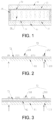
- 11 first substrate; 21: first metal film layer; 31: first alignment layer; 12: second substrate; 22: second metal film layer; 32: second alignment layer; 11: first through hole; 211: metal pattern; 212: first alignment mark; 40: sealant; 50: liquid crystal layer; 61: first adhesive layer; 611: first opening; and 71: first carrier layer.
- the present specific embodiment provides a liquid crystal phase shifter.
- the liquid crystal phase shifter includes a first substrate 11 and a second substrate 12 which are disposed oppositely, and further includes a liquid crystal layer 50 located between the first substrate 11 and the second substrate 12.
- Sealant 40 is further disposed between the first substrate 11 and the second substrate 12.
- the sealant 40 is located at the edges of the first substrate 11 and the second substrate 12, and is used for sealing the liquid crystal layer 50.
- supports containing plastic balls and the epoxy sealant 40 are distributed in the liquid crystal layer 50.
- the first substrate 11 is provided with a first conductive layer
- the second substrate 12 is provided with a second conductive layer.
- the side of the first substrate 11 facing the second substrate 12 is provided with a first metal film layer 21, and the side of the second substrate 12 facing the first substrate 11 is provided with a second metal film layer 22.
- the first metal film layer 21 and the second metal film layer 21 are both patterned metal film layers.
- the first substrate 11 and the second substrate 12 are made of a material with relatively good stability and insulating effect and extremely low dielectric loss.
- the first substrate 11 and the second substrate 12 may be glass substrates, fused quartz, ABS, ceramic base materials, and ceramic thermosetting polymer composite materials.
- the first substrate 11 and the second substrate 12 are preferably PCBs.
- the PCBs used in the present application are used as the substrates of the liquid crystal phase shifter.
- the dielectric constants and the dielectric loss of the PCBs are less than those of the glass substrate usually used by a liquid crystal panel, so that the PCBs are lower in dielectric loss, which is favorable for improving the performance of the liquid crystal phase shifter and a liquid crystal antenna in ultra-high frequency band application.
- the PCBs used as the substrates of the liquid crystal phase shifter may be FR4 (epoxy resin glass fiber) boards, PTFE (polytetrafluoroethylene) boards, PPS (polyphenylene sulfide), PS (polystyrene), PPO (polyphenylene oxide), and other boards, but the PCBs are preferably high-frequency boards, and PTFE high-frequency boards are preferred.
- the PTFE high-frequency boards have lower dielectric constant and dielectric loss. The lower dielectric loss may further improve the performance of the liquid crystal phase shifter and the liquid crystal antenna in the ultra-high frequency band application.
- the first metal film layer 21 and the second metal film layer 22 are made of metal materials with high conductivity and magnetic permeability, and may be made of metals such as aluminum, copper, silver, gold, cadmium, chromium, molybdenum, niobium, nickel, iron, etc., preferably silver, copper, gold, aluminum and their alloys.
- the metal materials of the metal film layers are preferably copper materials.
- the first metal film layer 21 and the second metal film layer 21 are both copper layers.
- the thicknesses of the metal materials and the metal film layers are related to the conductor loss, and the skin effect is a reflection of the conductor loss. Since alternating current has the skin effect, the skin effect indirectly increases the resistance of a conductor, and its energy heat loss also increases accordingly. In high-frequency bands such as microwaves, the skin effect is very obvious. Different metal materials have different skin depths.
- Skin effect when there is alternating current or an alternating electromagnetic field in the conductor, the current distribution inside the conductor is not uniform. The current is concentrated on the outer skin portion of the conductor. The closer to the surface of the conductor is, the greater the current density is. The current inside the conductor wire is actually very low. As a result, the resistance of the conductor increases, and the power loss of the conductor also increases. This phenomenon is the skin effect.
- the skin effect required by the liquid crystal phase shifter and the liquid crystal antenna generally requires that the thicknesses of the metal film layers of the corresponding first metal film layer 21 and second metal film layer 22 are respectively 3 to 5 times the skin depth ⁇ .
- the thicknesses of the metal film layers must reach a film thickness of ⁇ m to better ensure the performance of the liquid crystal antenna.
- the thicknesses of the metal film layers of the first metal film layer 21 and the second metal film layer 22 are not less than 2.0 ⁇ m.
- an oppositely bonding and bonding mechanism needs to perform transparent mark capturing from the backs of the two substrates (that is, from the surfaces, back on to the corresponding metal film layers, of the substrates). Since the PCBs are light-proof, it is not favorable for the oppositely bonding of the two substrates by using the transparent mark capturing method, causing a failure of accurate alignment, which cannot meet the design requirements of the antenna and then greatly reduces the performance of the antenna. If manual blind bonding is used, the accuracy of bonding cannot be guaranteed.
- the first metal film layer 21 is provided with a first alignment mark 212
- the second metal film layer 22 is provided with a second alignment mark.
- the position, corresponding to the first alignment mark 212, of the first substrate 11 is provided with a first through hole 111
- the position, corresponding to the second alignment mark, of the second substrate 12 is provided with a second through hole.
- the alignment marks may be round marks. Or, the alignment marks may also include marking lines in two directions perpendicular to each other. For example, the alignment marks may be cross marks, or two lines at an included angle of 90 degrees.
- This application solves the problem of light transmittance by respectively disposing the alignment marks on the first metal film layer 21 and the second metal film layer 22, and respectively forming the through holes in positions, corresponding to the alignment marks, on the first substrate 11 and the second substrate 12, so that the oppositely bonding mechanism can align the two substrates and then assemble the two aligned substrates through the transparent mark capturing, and then a process of bonding the two substrates to form cells can be favorably implemented.
- the first substrate 11 and the second substrate 12 are oppositely bonded by using a CCD lens.
- the first substrate 11 is taken as an example.
- the CCD lens performs the transparent mark capturing from the first substrate 11 on the back of the first metal film layer 21, and can see the first alignment mark 212 through the first through hole 111 in the first substrate 11.
- the first through hole 111 completely covers the first alignment mark 212: assuming that there is a virtual plane, the plane, for example, is a plane where the first substrate 11 is located. A projection of the first through hole 111 on the plane can completely cover a projection of the first alignment mark 212 on this plane. Similarly, the second through hole completely covers the second alignment mark.
- the first alignment mark 212 and the second alignment mark will be described as follows.
- the first alignment mark 212 may be disposed on the surface, close to the first substrate 11, of the first metal film layer 21, so it can be seen through the first through hole 111.
- a via hole is manufactured as an alignment mark, or only a partially transparent region is manufactured as an alignment mark, or an alignment mark is manufactured through laser, and the like.
- the second alignment mark may be disposed on the surface, close to the second substrate 12, of the second metal film layer 22, so it can be seen through the second through hole.
- the alignment marks are metal alignment marks obtained by performing exposure and etching on the corresponding metal film layers.
- the first alignment mark 212 is obtained by performing the exposure and etching on the first metal film layer 21, and the second alignment mark is obtained by performing the exposure and etching on the second metal film layer 22, and the first alignment mark 212 and the second alignment mark are metal alignment marks. It can be understood that the position of the first alignment mark 212 corresponds to the position of the second alignment mark.
- the first substrate 11 is taken as an example.
- a transparent first carrier layer 71 is arranged between the first metal film layer 21 and the first substrate 11.
- the size of the metal alignment mark is generally smaller than the size of the through hole.
- the first carrier layer 71 and the second carrier layer may be PI (polyimide) layers, PET (polyethylene terephthalate) layers, or PE (polyethylene) layers, all of which have good light transmittance.
- PI polyimide
- PET polyethylene terephthalate
- PE polyethylene
- the first carrier layer 71 and the second carrier layer are the PI layers, and PI has the advantages of better light transmittance, good high-temperature resistance, and the like.
- an integrated copper-cladded PI base material may be used, that is, the PI base material layer is clad with a copper foil layer in a laminating manner, and the copper foil-cladded PI base material can replace the first carrier layer 71 and the first metal film layer 21, and cause the first carrier layer 71 and the first metal film layer 21 to be integrated.
- the copper foil-cladded PI base material may be attached to the corresponding substrate through an adhesive layer. As shown in FIG. 3 , there is a first adhesive layer 61 between the first carrier layer 71 and the first substrate 11, and the first carrier layer 71 is attached to the first substrate 11 through the first adhesive layer 61. Similarly, there is a second adhesive layer between the second carrier layer and the second substrate 12.
- a carrier layer such as a PI layer
- a metal film layer may be manufactured or disposed on the carrier layer.
- this solution is that since the copper foil-cladded PI base material is generally an existing board, it may be purchased directly.
- this solution has the advantages of low cost and more time saving.
- the first adhesive layer 61 and the second adhesive layer may be non-transparent adhesives commonly used in the PCBs, or may be transparent optical adhesives.
- the position, corresponding to the first alignment mark 212, of the first adhesive layer 61 is provided with a first opening 611
- the position, corresponding to the second alignment mark, of the second adhesive layer is provided with a second opening.
- the arrangement of the first opening 611 and the second opening causes the first adhesive layer 61 and the second adhesive layer not to hinder the transparent mark capturing based oppositely bonding
- the first opening 611 completely covers the first alignment mark 212: assuming that there is a virtual plane, the plane, for example, is a plane where the first substrate 11 is located. A projection of the first opening 611 on the plane can completely cover a projection of the first alignment mark 212 on this plane. Similarly, the second opening completely covers the second alignment mark.
- the first opening 611 is not smaller than the first through hole 111 in the first substrate 11, and the second opening is not smaller than the second through hole in the second substrate 12.
- the first through hole 111, the second through hole, the first opening 611 and the second opening are preferably manufactured before the carrier layers are attached, so as to prevent damage to the carrier layers or the metal film layers when the through holes or the openings are manufactured.
- the manufacturing method of the liquid crystal phase shifter further includes the steps of hot-pressing cell formation, small piece cutting, filling and sealing, binding, and the like. It should be noted that the abovementioned arrangement of the first alignment mark 212, the second alignment mark, the first through hole 111 and the second through hole, and the arrangement of the first opening 611 and the second opening are to facilitate the transparent mark capturing of the alignment and bonding mechanism from the backs of the substrates during the oppositely bonding of the two substrates of the liquid crystal phase shifter, so as to realize precise alignment of the first substrate and the second substrate.
- the first alignment mark 212, the second alignment mark, the first through hole 111, and the second through hole are generally disposed at the edge positions of a liquid crystal phase shifter product. During subsequent small piece cutting, the first alignment mark 212, the second alignment mark, the first through hole 111 and the second through hole are generally cut off.
- the liquid crystal phase shifter further includes a first alignment layer 31 and a second alignment layer 32 which are disposed on two sides of the liquid crystal layer 50, respectively.
- the first alignment layer 31 is prepared on the first substrate 11 on which the patterned metal film layer is formed
- the second alignment layer 32 is prepared on the second substrate 12 on which the patterned metal film layer is formed.
- the alignment layer is used to define an initial deflection angle of crystal molecules of the liquid crystal layer 50.
- metal patterns 211 on the patterned second metal film layer 22 include a phase shifter electrode.
- the phase shifter electrode is a planar transmission line used for transmitting microwave signals.
- the planar transmission line is preferably a microstrip line.
- the shape of the microstrip line may be of an S shape or a spiral shape.
- the shape of the microstrip line is not limited, as long as it may realize transmission of the microwave signals.
- Metal patterns 211 on the patterned first metal film layer 21 include a grounding electrode, and the liquid crystal phase shifter further includes an offset line.
- the offset line may be disposed on the second metal film layer 22 of the second substrate 12.
- the liquid crystal molecules are arranged in a preset direction under the action of the first alignment layer and the second alignment layer.
- the electric field drives the deflection of the liquid crystal molecules in the liquid crystal layer 50.
- the microwave signal is transmitted between the microstrip line and the grounding electrode. During the transmission of the microwave signal, the phase will be changed due to the deflection of the liquid crystal molecules, thereby realizing a phase shift function of the microwave signal.
- the deflection angle of the liquid crystals in the liquid crystal layer 50 can be controlled, and thus the phase adjusted during the phase shifting can be controlled.
- the effective dielectric constant of the liquid crystals is changed by controlling the voltage applied to the liquid crystal layer 50, thereby controlling the phase adjusted during the phase shifting.
- a two-dimensional pattern is formed by specially designed liquid crystal antenna units with different electrostatic capacitances. Electromagnetic waves received or emitted from the antenna are endowed with a phase difference corresponding to the electrostatic capacitance of each antenna unit, and the two-dimensional pattern formed by the antenna elements with the different electrostatic capacitances has strong directivity (beam scanning) in a specific direction, thereby realizing a mutual conversion function between the electromagnetic waves received or emitted from the antenna and a radio frequency signal (a voltage signal).
- the present disclosure has the following beneficial effects.
- the present specific embodiment provides a liquid crystal antenna.
- the liquid crystal antenna includes the liquid crystal phase shifter in Embodiment I.
- the liquid crystal antenna further includes an antenna radiation unit used for radiating a microwave signal, thereby realizing feed-in and feed-out of the microwave signal.
- the side, away from the second substrate 12, of the first substrate 11 is provided with an antenna radiation unit.
- the antenna radiation unit is made of a high-conductivity material.
- the antenna radiation unit may be a rectangular, round, or square patch, may realize corner cutting, and may also be attached to the liquid crystal phase shifter by a patch process.
- a more preferable solution is that the antenna radiation unit is a patterned third metal film layer disposed on the side, away from the second substrate 12, of the first substrate 11.
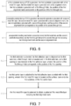
- the present specific embodiment provides a manufacturing method of the liquid crystal phase shifter in Embodiment I. As shown in FIG. 6 , the manufacturing method of the liquid crystal phase shifter includes the following steps.
- the first metal film layer 21 is provided with a first alignment mark 212.
- the first substrate 11 is provided with a first through hole 111.
- the position of the first alignment mark 212 corresponds to the position of the first through hole 111.
- Step S2 a second substrate 12 being a PCB is provided.
- the second substrate 12 is provided with a second metal film layer 22, the second metal film layer 22 is provided with a second alignment mark.
- the second substrate 12 is provided with a second through hole, and the position of the second alignment mark corresponds to the position of the second through hole.
- Step S3 an oppositely bonding and bonding mechanism oppositely bonds the first substrate 11 and the second substrate 12 respectively via the first through hole 111 and the second through hole by using the first alignment mark 212 and the second alignment mark and then assembles the aligned first substrate and second substrate.
- CCD transparent alignment usually used in oppositely bonding of the liquid crystal panel is used to implement accurate bonding: a CCD lens is used.
- the CCD lens pre-aligns the first substrate 11 and the second substrate 12 respectively via the first through hole 111 and the second through hole by using the first alignment mark 212 and the second alignment mark, and the first substrate 11 and the second substrate 12 slowly move to a bonded state after the alignment.
- the first alignment mark 212 may be disposed on the surface, close to the first substrate 11, of the first metal film layer 21, so it can be seen through the first through hole 111.
- a via hole is manufactured as an alignment mark, or only a partially transparent region is manufactured as an alignment mark, or an alignment mark is manufactured through laser, and the like.
- the second alignment mark may be disposed on the surface, close to the second substrate 12, of the second metal film layer 22, so it can be seen through the second through hole.
- the alignment marks are metal alignment marks obtained by performing exposure and etching on the corresponding metal film layers.
- the first alignment mark 212 is obtained by performing the exposure and etching on the first metal film layer 21, and the second alignment mark is obtained by performing the exposure and etching on the second metal film layer 22, and both the first alignment mark 212 and the second alignment mark are metal alignment marks.
- the size of the metal alignment marks is generally smaller than that of the through holes, so as to perform the transparent mark capturing via the through holes.
- metals at the peripheries of the metal alignment marks are etched away, so that the metal alignment marks are not supported.
- a transparent first carrier layer 71 is arranged between the first metal film layer 21 and the first substrate 11, and a transparent second carrier layer is arranged between the second metal film layer 22 and the second substrate 12.
- the first carrier layer 71 and the second carrier layer may be PI layers, PET layers, or PE layers, all of which have good light transmittance.
- the first carrier layer 71 and the second carrier layer are the PI layers, and PI has the advantages of better light transmittance, good high-temperature resistance, and the like, and can endure high-temperature baking in a subsequent alignment layer manufacturing process.
- copper foil-cladded PI base materials may be used as the metal film layers and the carrier layers.
- the copper foil-cladded PI base materials are obtained by cladding PI base material layers with copper foil layers in a laminating manner.
- the copper foil-cladded PI base materials may be attached to the corresponding substrates through adhesive layers. Specifically, a first adhesive layer 61 is arranged between the first carrier layer 71 and the first substrate 11, and a second adhesive layer is arranged between the second carrier layer and the second substrate 12.
- a carrier layer such as a PI layer
- a metal film layer may be manufactured or disposed on the carrier layer.
- step S1 includes the following steps.
- Step S11 the first substrate 11 is provided, the first adhesive layer 61 is disposed on the first substrate 11, a first through hole 111 is manufactured in the first substrate 11, and a first opening 611 is manufactured in the first adhesive layer 61, wherein the position of the first through hole 111 corresponds to the position of the first opening 611.
- Step S12 the first carrier layer 71 is attached to the first adhesive layer 61 provided with the first opening 611, wherein the first metal film layer 21 is located on the surface, back on to the first substrate 11, of the first carrier layer 71.
- Step S13 the first metal film layer 21 is patterned to obtain a patterned first metal film layer 21 including the first alignment mark 212.
- step S11 the first through hole 111 and the first opening 611 may be manufactured at the same time, or manufactured in sequence.
- the first metal film layer 21 and the first carrier layer 71 may be a whole.
- the first carrier layer 71 is attached to the first adhesive layer 61.
- the copper foil-cladded PI base material is directly used to be attached to the first adhesive layer 61.
- the first metal film layer 21 is manufactured or disposed on the first carrier layer 71.
- step S2 includes the following steps.
- Step S21 the second substrate 12 is provided, a second adhesive layer is disposed on the second substrate 12, a second through hole is manufactured in the second substrate 12, and a second opening is manufactured in the second adhesive layer, wherein the position of the second through hole corresponds to the position of the second opening.
- Step S22 the second carrier layer is attached to the second adhesive layer provided with the second opening, wherein the second metal film layer 22 is located on the surface, back on to the second substrate 12, of the second carrier layer.
- Step S23 the second metal film layer 22 is patterned to obtain a patterned second metal film layer 22 including the second alignment mark.
- the second through hole and the second opening may be manufactured at the same time, or manufactured in sequence.
- the second metal film layer 22 and the second carrier layer may be a whole.
- the second carrier layer is attached to the second adhesive layer.
- the copper foil-cladded PI base material is directly used to be attached to the second adhesive layer.
- the second metal film layer 22 is manufactured or disposed on the second carrier layer.
- the manufacturing method of the liquid crystal phase shifter further includes a specific process for patterning the first metal film layer 21 and the second metal film layer 22, and further includes a process step of manufacturing alignment layers and sealant 40 after the metal film layers are patterned.
- the process method for patterning the metal film layers is known to those skilled in the art, and can be obtained through processes of photoresist coating, precuring, exposure, developing, etching, and stripping.
- the alignment layers may be manufactured by using a PI rubbing process in the prior art to form an alignment groove on the surface.
- an APR board may be used to transfer preset dripping alignment liquid onto the corresponding substrates with the metal patterns, and causes the liquid to fully react through high-temperature baking. Meanwhile, solvents are volatilized, and solid alignment film layers are finally formed.
- the alignment film is polished with velvet cloth or cotton cloth in one direction, and finally the liquid crystal molecules are arranged in parallel according to a preset polishing direction, which will not be repeated here.
- the manufacturing method of the liquid crystal phase shifter further includes the steps of hot-pressing cell formation, small-piece cutting, filling and sealing, binding, and the like.
- the first substrate 11 and the second substrate 12 are generally large-sized substrates.
- a large board is used.
- the manufacturing method of the liquid crystal phase shifter further includes the steps of hot-pressing cell formation, small-piece cutting, filling and sealing, binding, and the like.
- pre-bonded substrates are cured by a high-pressure and high-temperature process, and a certain cell gap will be formed. After sufficient curing, a plurality of cells with high bonding strength and high mechanical strength will eventually be formed. Then, a plurality of single-grained liquid crystal phase shifter cells can be obtained through the small-piece cutting process.
- the abovementioned arrangement of the first alignment mark 212, the second alignment mark, the first through hole 111 and the second through hole, and the arrangement of the first opening 611 and the second opening are to facilitate the transparent mark capturing of the oppositely bonding and bonding mechanism from the backs of the substrates during the oppositely bonding of the two substrates of the liquid crystal phase shifter, so as to realize precise alignment of the first substrate and the second substrate.
- FIG. 5 illustrates a schematic diagram of a first substrate 11 of a large-sized substrate.
- the large-sized substrate includes a plurality of independent units.
- the first through hole 111 is located at the edge position of the large-sized substrate.
- Four independent units are illustrated in FIG. 5 only, and each unit includes independent sealant 40, but the number of sealant is not limited to this.
- the first alignment mark 212, the second alignment mark, the first through hole 111, and the second through hole are cut off, and do not exist in the liquid crystal phase shifter product.
- the present disclosure has the following beneficial effects.
- the present disclosure provides the manufacturing method for manufacturing the liquid crystal phase shifters in batches by using the PCBs as the substrates and combining the liquid crystal panel.
- the dielectric constants and the dielectric loss of the PCBs are less than those of the glass substrate usually used by the liquid crystal panel, so that the PCBs are lower in dielectric loss, which is favorable for improving the performance of the liquid crystal phase shifter in ultra-high frequency band application.
- the present disclosure further solves the problem that original non-transparent PCBs cannot use the transparent oppositely bonding and bonding mechanism of the liquid crystal panel to implement accurate bonding of the two substrates.
- the alignment marks are respectively disposed on the first metal film layer and the second metal film layer, and the through holes corresponding to the alignment marks in position are respectively disposed in the first substrate and the second substrate, so that the two substrates can be oppositely bonded by using the transparent mark capturing after the improvement.
- the alignment marks are the metal alignment marks obtained by performing exposure and etching on the corresponding metal film layers.
- the size of the metal alignment marks is smaller than that of the through holes.
Landscapes
- Physics & Mathematics (AREA)
- Nonlinear Science (AREA)
- Engineering & Computer Science (AREA)
- Manufacturing & Machinery (AREA)
- Chemical & Material Sciences (AREA)
- Crystallography & Structural Chemistry (AREA)
- General Physics & Mathematics (AREA)
- Optics & Photonics (AREA)
- Mathematical Physics (AREA)
- Liquid Crystal (AREA)
- Waveguide Switches, Polarizers, And Phase Shifters (AREA)
- Variable-Direction Aerials And Aerial Arrays (AREA)
Claims (6)
- Herstellungsverfahren für einen Flüssigkristall-Phasenschieber, das zur Herstellung des Flüssigkristall-Phasenschiebers verwendet wird, wobei das Herstellungsverfahren die folgenden Schritte einschließt:Schritt S0: Bereitstellen einer Flüssigkristallschicht (50) ;Schritt S1: Bereitstellen eines ersten Substrats (11), das eine Leiterplatte (PCB) ist, wobei das erste Substrat mit einer ersten Metallfilmschicht (21) versehen ist, die erste Metallfilmschicht mit einer ersten Ausrichtungsmarkierung (212) versehen ist, das erste Substrat (11) mit einem ersten Durchgangsloch (111) versehen ist und eine Position der ersten Ausrichtungsmarkierung einer Position des ersten Durchgangslochs (111) entspricht;Schritt S2: Bereitstellen eines zweiten Substrats (12), das eine Leiterplatte ist, wobei das zweite Substrat mit einer zweiten Metallfilmschicht (22) versehen ist, die zweite Metallfilmschicht mit einer zweiten Ausrichtungsmarkierung versehen ist, das zweite Substrat (12) mit einem zweiten Durchgangsloch versehen ist und eine Position der zweiten Ausrichtungsmarkierung einer Position des zweiten Durchgangslochs entspricht; undSchritt S3: Verbinden des ersten Substrats (11) und des zweiten Substrats (12) jeweils über das erste Durchgangsloch (111) und das zweite Durchgangsloch unter Verwendung der ersten Ausrichtungsmarkierung (212) und der zweiten Ausrichtungsmarkierung und Verbinden des ausgerichteten ersten Substrats und zweiten Substrats, wobei die Flüssigkristallschicht (50) zwischen dem ersten Substrat (11) und dem zweiten Substrat (12) angeordnet ist und die Metallfilmschichten (21, 22) in dem ersten und zweiten Substrat (11, 12) jeweils auf den Seiten der Substrate (11, 12) angeordnet sind, die einander zugewandt sind;und wobei die erste Ausrichtungsmarkierung (212) eine Metallausrichtungsmarkierung ist und die erste Ausrichtungsmarkierung (212) durch Ausführen von Belichtung und Ätzen auf der ersten Metallfilmschicht (21) ermittelt wird;die zweite Ausrichtungsmarkierung eine Metallausrichtungsmarkierung ist, und die zweite Ausrichtungsmarkierung durch Ausführen von Belichtung und Ätzen auf der zweiten Metallfilmschicht (22) ermittelt wird;eine erste Trägerschicht (71) mit hoher Lichtdurchlässigkeit zwischen der ersten Metallfilmschicht (21) und dem ersten Substrat (11) angeordnet ist, und die erste Trägerschicht (71) als unterstützende Schicht der ersten Ausrichtungsmarkierung (212) verwendet wird; undein zweiter Träger mit hoher Lichtdurchlässigkeit zwischen der zweiten Metallfilmschicht (22) und dem zweiten Substrat (12) angeordnet ist, und die zweite Trägerschicht als unterstützende Schicht der zweiten Ausrichtungsmarkierung verwendet wird.
- Herstellungsverfahren für einen Flüssigkristall-Phasenschieber nach Anspruch 1, dadurch gekennzeichnet, dass der Schritt S1 die folgenden Schritte einschließt:Bereitstellen des ersten Substrats (11), Anordnen einer ersten Klebstoffschicht (61) auf dem ersten Substrat, Herstellen eines ersten Durchgangslochs (111) in dem ersten Substrat (11), und Herstellen einer ersten Öffnung (611) in der ersten Klebstoffschicht (61), wobei die Position des ersten Durchgangslochs (111) einer Position der ersten Öffnung (611) entspricht;Verbinden der ersten Trägerschicht (71) mit der ersten Klebstoffschicht (61), die mit der ersten Öffnung (611) versehen ist, wobei sich die erste Metallfilmschicht (21) auf der Oberfläche der ersten Trägerschicht auf der Rückseite des ersten Substrats (11) befindet; undStrukturieren der ersten Metallfilmschicht (21), um eine strukturierte erste Metallfilmschicht zu ermitteln, die die erste Ausrichtungsmarkierung (212) einschließt;der Schritt S2 die folgenden Schritte einschließt:Bereitstellen des zweiten Substrats (12), Anordnen einer zweiten Klebstoffschicht auf dem zweiten Substrat, Herstellen eines zweiten Durchgangslochs in dem zweiten Substrat (12) und Herstellen einer zweiten Öffnung in der zweiten Klebstoffschicht, wobei die Position des zweiten Durchgangslochs einer Position der zweiten Öffnung entspricht;Verbinden der zweiten Trägerschicht mit der zweiten Klebstoffschicht, die mit der zweiten Öffnung versehen ist, wobei sich die zweite Metallfilmschicht (22) auf der Oberfläche der zweiten Trägerschicht auf der Rückseite des zweiten Substrats (12) befindet; undStrukturieren der zweiten Metallfilmschicht (22), um eine strukturierte zweite Metallfilmschicht zu ermitteln, die die zweite Ausrichtungsmarkierung einschließt.
- Herstellungsverfahren für einen Flüssigkristall-Phasenschieber nach Anspruch 2, dadurch gekennzeichnet, dass das erste Durchgangsloch (111) die erste Ausrichtungsmarkierung (212) vollständig abdeckt, und das zweite Durchgangsloch die zweite Ausrichtungsmarkierung vollständig abdeckt.
- Herstellungsverfahren für einen Flüssigkristall-Phasenschieber nach Anspruch 1, dadurch gekennzeichnet, dass beim gegenseitigen Verbinden des ersten Substrats (11) und des zweiten Substrats (12) im Schritt S3 ein großformatiges Substrat verwendet wird;
nach dem Schritt S3 das Herstellungsverfahren ferner einen Heißpress-Zellenbildungsschritt einschließt, um eine Vielzahl von Zellen herzustellen, und dann werden Flüssigkristall-Phasenschieberzellen mit einzelnen Körnern durch einen kleinteiligen Schneidprozess ermittelt. - Herstellungsverfahren für einen Flüssigkristall-Phasenschieber nach Anspruch 4, dadurch gekennzeichnet, dass die erste Ausrichtungsmarkierung (212), die zweite Ausrichtungsmarkierung, das erste Durchgangsloch (111) und das zweite Durchgangsloch an einer Position an der Kante des großformatigen Substrats während der Herstellung einer großen Platte angeordnet sind;
während des Prozesses des Kleinteileschneidens werden die erste Ausrichtungsmarkierung (212), die zweite Ausrichtungsmarkierung, das erste Durchgangsloch (111) und das zweite Durchgangsloch abgeschnitten. - Herstellungsverfahren für einen Flüssigkristall-Phasenschieber nach einem der Ansprüche 1 bis 5, dadurch gekennzeichnet, dass die erste Trägerschicht (71) und die zweite Trägerschicht Polyimid (PI)-Schichten sind.
Applications Claiming Priority (2)
| Application Number | Priority Date | Filing Date | Title |
|---|---|---|---|
| CN201910272556.9A CN110034358B (zh) | 2019-04-04 | 2019-04-04 | 一种液晶移相器、液晶天线及液晶移相器的制作方法 |
| PCT/CN2019/082162 WO2020199238A1 (zh) | 2019-04-04 | 2019-04-11 | 一种液晶移相器、液晶天线及液晶移相器的制作方法 |
Publications (3)
| Publication Number | Publication Date |
|---|---|
| EP3745527A1 EP3745527A1 (de) | 2020-12-02 |
| EP3745527A4 EP3745527A4 (de) | 2021-01-13 |
| EP3745527B1 true EP3745527B1 (de) | 2023-11-15 |
Family
ID=67237510
Family Applications (1)
| Application Number | Title | Priority Date | Filing Date |
|---|---|---|---|
| EP19863992.4A Active EP3745527B1 (de) | 2019-04-04 | 2019-04-11 | Flüssigkristallphasenschieber, flüssigkristallantenne und herstellungsverfahren für einen flüssigkristallphasenschieber |
Country Status (7)
| Country | Link |
|---|---|
| US (1) | US11398677B2 (de) |
| EP (1) | EP3745527B1 (de) |
| JP (1) | JP6992184B2 (de) |
| KR (1) | KR102353469B1 (de) |
| CN (1) | CN110034358B (de) |
| TW (1) | TWI730700B (de) |
| WO (1) | WO2020199238A1 (de) |
Families Citing this family (17)
| Publication number | Priority date | Publication date | Assignee | Title |
|---|---|---|---|---|
| CN119209036A (zh) * | 2019-09-05 | 2024-12-27 | 群创光电股份有限公司 | 电子装置 |
| CN110707397B (zh) * | 2019-10-17 | 2023-02-17 | 京东方科技集团股份有限公司 | 液晶移相器及天线 |
| CN113871817B (zh) * | 2020-06-30 | 2022-07-19 | 上海天马微电子有限公司 | 移相器及制作方法、天线 |
| CN114079159B (zh) | 2020-08-13 | 2022-11-11 | 上海天马微电子有限公司 | 液晶天线 |
| CN114388996B (zh) * | 2020-10-22 | 2023-04-07 | 上海天马微电子有限公司 | 液晶移相器及其制作方法、液晶天线 |
| CN114614245B (zh) * | 2020-12-04 | 2023-10-13 | 上海中航光电子有限公司 | 一种天线及其制作方法 |
| CN112909554B (zh) * | 2021-02-22 | 2022-09-13 | 成都天马微电子有限公司 | 一种天线及其制作方法 |
| CN113104332A (zh) * | 2021-04-23 | 2021-07-13 | 深圳市精运达自动化设备有限公司 | 一种显示屏加工工艺 |
| EP4353475A4 (de) * | 2021-06-08 | 2025-05-21 | Agc Inc. | Substrat für hochfrequenzvorrichtung |
| CN114006163B (zh) | 2021-11-22 | 2024-08-13 | 上海天马微电子有限公司 | 液晶天线及其制作方法 |
| CN114069231A (zh) * | 2021-11-26 | 2022-02-18 | 北京华镁钛科技有限公司 | 一种平面透镜天线 |
| US12580304B2 (en) * | 2021-12-23 | 2026-03-17 | Beijing Boe Technology Development Co., Ltd. | Liquid crystal antenna |
| CN114284714B (zh) | 2021-12-31 | 2023-12-15 | 成都天马微电子有限公司 | 液晶天线及其制备方法 |
| WO2023155109A1 (zh) | 2022-02-17 | 2023-08-24 | 京东方科技集团股份有限公司 | 移相器、天线及电子设备 |
| KR102730475B1 (ko) | 2022-11-22 | 2024-11-14 | 충남대학교 산학협력단 | 액정 기반 평면 회로의 성능 측정 장치 |
| KR102837708B1 (ko) | 2022-11-30 | 2025-07-24 | 충남대학교 산학협력단 | 고속 액정형 위상변위기 |
| TWI852585B (zh) * | 2023-05-25 | 2024-08-11 | 友達光電股份有限公司 | 液晶移相器 |
Family Cites Families (25)
| Publication number | Priority date | Publication date | Assignee | Title |
|---|---|---|---|---|
| US6356166B1 (en) * | 1999-08-26 | 2002-03-12 | Metawave Communications Corporation | Multi-layer switched line phase shifter |
| TWI289696B (en) | 2001-06-12 | 2007-11-11 | Himax Tech Ltd | Fabricating apparatus and method for a liquid crystal display panel |
| KR20060086712A (ko) * | 2005-01-27 | 2006-08-01 | 삼성에스디아이 주식회사 | 직부착 필터 얼라인 마크가 형성된 디스플레이 패널 모듈 |
| EP2575211B1 (de) * | 2011-09-27 | 2014-11-05 | Technische Universität Darmstadt | Elektronisch steuerbare Planarphasen-Arrayantenne |
| US9059496B2 (en) * | 2011-11-14 | 2015-06-16 | The Regents Of The University Of Colorado | Nanoparticle-enhanced liquid crystal radio frequency phase shifter |
| EP2768072A1 (de) * | 2013-02-15 | 2014-08-20 | Technische Universität Darmstadt | Phasenschieber |
| US10714838B2 (en) | 2014-10-30 | 2020-07-14 | Mitsubishi Electric Corporation | Array antenna apparatus and method of manufacturing the same |
| US9755286B2 (en) | 2014-12-05 | 2017-09-05 | Huawei Technologies Co., Ltd. | System and method for variable microwave phase shifter |
| US10170826B2 (en) * | 2015-10-09 | 2019-01-01 | Sharp Kabushiki Kaisha | TFT substrate, scanning antenna using same, and method for manufacturing TFT substrate |
| WO2017065255A1 (ja) * | 2015-10-15 | 2017-04-20 | シャープ株式会社 | 走査アンテナおよびその製造方法 |
| US20210181551A1 (en) | 2016-10-04 | 2021-06-17 | Jsr Corporation | Liquid crystal device and method of manufacture therefor |
| KR102364013B1 (ko) * | 2016-12-07 | 2022-02-16 | 웨이퍼 엘엘씨 | 저손실 전기 전송 메커니즘과 이를 이용한 안테나 |
| US11049658B2 (en) | 2016-12-22 | 2021-06-29 | Kymeta Corporation | Storage capacitor for use in an antenna aperture |
| CN110192306B (zh) * | 2017-01-13 | 2021-02-05 | 夏普株式会社 | 扫描天线和扫描天线的制造方法 |
| CN108321503B (zh) * | 2017-01-16 | 2020-05-15 | 群创光电股份有限公司 | 液晶天线装置 |
| US10476136B2 (en) * | 2017-07-20 | 2019-11-12 | Apple Inc. | Electronic device with speaker port aligned antennas |
| JP6596048B2 (ja) * | 2017-09-05 | 2019-10-23 | シャープ株式会社 | アライメントマーク付き基板の製造方法 |
| CN108490706B (zh) * | 2018-04-13 | 2024-04-02 | 京东方科技集团股份有限公司 | 液晶移相器及其制造方法、液晶天线及电子装置 |
| CN108493592B (zh) * | 2018-05-03 | 2019-12-20 | 京东方科技集团股份有限公司 | 微带天线及其制备方法和电子设备 |
| CN108767456B (zh) * | 2018-05-07 | 2020-07-31 | 电子科技大学 | 一种可分块控制的方向图可重构液晶天线及重构方法 |
| CN110518311B (zh) * | 2018-05-21 | 2025-01-28 | 京东方科技集团股份有限公司 | 一种移相器及其工作方法、天线、通信设备 |
| CN109932845B (zh) * | 2018-06-08 | 2020-12-01 | 京东方科技集团股份有限公司 | 液晶移相器及电子装置 |
| CN108803096B (zh) | 2018-06-27 | 2020-06-26 | 成都天马微电子有限公司 | 一种液晶移相单元及其制作方法、液晶移相器及天线 |
| CN108808181B (zh) * | 2018-07-20 | 2020-05-29 | 成都天马微电子有限公司 | 液晶移相器和天线 |
| CN209544568U (zh) * | 2019-04-04 | 2019-10-25 | 信利半导体有限公司 | 一种液晶移相器和液晶天线 |
-
2019
- 2019-04-04 CN CN201910272556.9A patent/CN110034358B/zh active Active
- 2019-04-11 EP EP19863992.4A patent/EP3745527B1/de active Active
- 2019-04-11 WO PCT/CN2019/082162 patent/WO2020199238A1/zh not_active Ceased
- 2019-04-11 KR KR1020207016583A patent/KR102353469B1/ko active Active
- 2019-04-11 JP JP2020531607A patent/JP6992184B2/ja active Active
- 2019-04-11 US US16/770,957 patent/US11398677B2/en active Active
-
2020
- 2020-03-30 TW TW109110778A patent/TWI730700B/zh active
Also Published As
| Publication number | Publication date |
|---|---|
| KR102353469B1 (ko) | 2022-01-19 |
| EP3745527A4 (de) | 2021-01-13 |
| CN110034358A (zh) | 2019-07-19 |
| KR20200117984A (ko) | 2020-10-14 |
| WO2020199238A1 (zh) | 2020-10-08 |
| TWI730700B (zh) | 2021-06-11 |
| EP3745527A1 (de) | 2020-12-02 |
| US20210234268A1 (en) | 2021-07-29 |
| US11398677B2 (en) | 2022-07-26 |
| JP6992184B2 (ja) | 2022-01-13 |
| JP2021520078A (ja) | 2021-08-12 |
| TW202043890A (zh) | 2020-12-01 |
| CN110034358B (zh) | 2024-02-23 |
Similar Documents
| Publication | Publication Date | Title |
|---|---|---|
| US11398677B2 (en) | Liquid crystal phase shifter, liquid crystal antenna and manufacturing method of liquid crystal phase shifter | |
| US11336010B2 (en) | Liquid crystal antenna, method for manufacturing the same, and electronic device | |
| CN209544568U (zh) | 一种液晶移相器和液晶天线 | |
| CN114696058B (zh) | 液晶天线和通信设备 | |
| US11916297B2 (en) | Liquid crystal antena and fabrication thereof | |
| Tian et al. | Flexible and reconfigurable frequency selective surface with wide angular stability fabricated with additive manufacturing procedure | |
| EP3736618A1 (de) | Flache flüssigkristallantenne und herstellungsverfahren dafür | |
| CN109782494B (zh) | 一种液晶移相器及其制作方法 | |
| US11469500B2 (en) | Liquid crystal antenna, manufacturing method thereof and communication device | |
| US11996610B2 (en) | Antenna and manufacturing method thereof | |
| US20180159239A1 (en) | Low loss electrical transmission mechanism and antenna using same | |
| US20190341693A1 (en) | Low cost dielectric for electrical transmission and antenna using same | |
| CN115693130A (zh) | 天线及通信设备 | |
| CN209544616U (zh) | 一种平板液晶天线 | |
| CN113871864B (zh) | 液晶天线及其制作方法 | |
| US12548902B2 (en) | Phase shifter, antenna, and electronic device | |
| EP3788677B1 (de) | Kostengünstiges dielektrikum für elektrische übertragung und antenne mit verwendung davon | |
| Kim et al. | Impedance-Modulating Patch Integration for Gain and Bandwidth Control of Antenna-in-Display in Millimeter-Wave Smartphones | |
| Jaggi et al. | electrically tunable and adaptive antennas using liquid crystals |
Legal Events
| Date | Code | Title | Description |
|---|---|---|---|
| STAA | Information on the status of an ep patent application or granted ep patent |
Free format text: STATUS: UNKNOWN |
|
| STAA | Information on the status of an ep patent application or granted ep patent |
Free format text: STATUS: THE INTERNATIONAL PUBLICATION HAS BEEN MADE |
|
| PUAI | Public reference made under article 153(3) epc to a published international application that has entered the european phase |
Free format text: ORIGINAL CODE: 0009012 |
|
| STAA | Information on the status of an ep patent application or granted ep patent |
Free format text: STATUS: REQUEST FOR EXAMINATION WAS MADE |
|
| 17P | Request for examination filed |
Effective date: 20200403 |
|
| AK | Designated contracting states |
Kind code of ref document: A1 Designated state(s): AL AT BE BG CH CY CZ DE DK EE ES FI FR GB GR HR HU IE IS IT LI LT LU LV MC MK MT NL NO PL PT RO RS SE SI SK SM TR |
|
| AX | Request for extension of the european patent |
Extension state: BA ME |
|
| A4 | Supplementary search report drawn up and despatched |
Effective date: 20201210 |
|
| RIC1 | Information provided on ipc code assigned before grant |
Ipc: H01P 11/00 20060101ALI20201204BHEP Ipc: H01Q 3/36 20060101ALI20201204BHEP Ipc: H01P 1/18 20060101AFI20201204BHEP |
|
| DAV | Request for validation of the european patent (deleted) | ||
| DAX | Request for extension of the european patent (deleted) | ||
| STAA | Information on the status of an ep patent application or granted ep patent |
Free format text: STATUS: EXAMINATION IS IN PROGRESS |
|
| 17Q | First examination report despatched |
Effective date: 20221118 |
|
| GRAP | Despatch of communication of intention to grant a patent |
Free format text: ORIGINAL CODE: EPIDOSNIGR1 |
|
| STAA | Information on the status of an ep patent application or granted ep patent |
Free format text: STATUS: GRANT OF PATENT IS INTENDED |
|
| INTG | Intention to grant announced |
Effective date: 20230717 |
|
| GRAS | Grant fee paid |
Free format text: ORIGINAL CODE: EPIDOSNIGR3 |
|
| GRAA | (expected) grant |
Free format text: ORIGINAL CODE: 0009210 |
|
| STAA | Information on the status of an ep patent application or granted ep patent |
Free format text: STATUS: THE PATENT HAS BEEN GRANTED |
|
| AK | Designated contracting states |
Kind code of ref document: B1 Designated state(s): AL AT BE BG CH CY CZ DE DK EE ES FI FR GB GR HR HU IE IS IT LI LT LU LV MC MK MT NL NO PL PT RO RS SE SI SK SM TR |
|
| REG | Reference to a national code |
Ref country code: CH Ref legal event code: EP Ref country code: GB Ref legal event code: FG4D |
|
| REG | Reference to a national code |
Ref country code: DE Ref legal event code: R096 Ref document number: 602019041660 Country of ref document: DE |
|
| REG | Reference to a national code |
Ref country code: IE Ref legal event code: FG4D |
|
| REG | Reference to a national code |
Ref country code: LT Ref legal event code: MG9D |
|
| REG | Reference to a national code |
Ref country code: NL Ref legal event code: MP Effective date: 20231115 |
|
| PG25 | Lapsed in a contracting state [announced via postgrant information from national office to epo] |
Ref country code: GR Free format text: LAPSE BECAUSE OF FAILURE TO SUBMIT A TRANSLATION OF THE DESCRIPTION OR TO PAY THE FEE WITHIN THE PRESCRIBED TIME-LIMIT Effective date: 20240216 |
|
| PG25 | Lapsed in a contracting state [announced via postgrant information from national office to epo] |
Ref country code: IS Free format text: LAPSE BECAUSE OF FAILURE TO SUBMIT A TRANSLATION OF THE DESCRIPTION OR TO PAY THE FEE WITHIN THE PRESCRIBED TIME-LIMIT Effective date: 20240315 |
|
| PG25 | Lapsed in a contracting state [announced via postgrant information from national office to epo] |
Ref country code: LT Free format text: LAPSE BECAUSE OF FAILURE TO SUBMIT A TRANSLATION OF THE DESCRIPTION OR TO PAY THE FEE WITHIN THE PRESCRIBED TIME-LIMIT Effective date: 20231115 |
|
| REG | Reference to a national code |
Ref country code: AT Ref legal event code: MK05 Ref document number: 1632630 Country of ref document: AT Kind code of ref document: T Effective date: 20231115 |
|
| PG25 | Lapsed in a contracting state [announced via postgrant information from national office to epo] |
Ref country code: NL Free format text: LAPSE BECAUSE OF FAILURE TO SUBMIT A TRANSLATION OF THE DESCRIPTION OR TO PAY THE FEE WITHIN THE PRESCRIBED TIME-LIMIT Effective date: 20231115 |
|
| PG25 | Lapsed in a contracting state [announced via postgrant information from national office to epo] |
Ref country code: AT Free format text: LAPSE BECAUSE OF FAILURE TO SUBMIT A TRANSLATION OF THE DESCRIPTION OR TO PAY THE FEE WITHIN THE PRESCRIBED TIME-LIMIT Effective date: 20231115 |
|
| PG25 | Lapsed in a contracting state [announced via postgrant information from national office to epo] |
Ref country code: ES Free format text: LAPSE BECAUSE OF FAILURE TO SUBMIT A TRANSLATION OF THE DESCRIPTION OR TO PAY THE FEE WITHIN THE PRESCRIBED TIME-LIMIT Effective date: 20231115 |
|
| PG25 | Lapsed in a contracting state [announced via postgrant information from national office to epo] |
Ref country code: NL Free format text: LAPSE BECAUSE OF FAILURE TO SUBMIT A TRANSLATION OF THE DESCRIPTION OR TO PAY THE FEE WITHIN THE PRESCRIBED TIME-LIMIT Effective date: 20231115 Ref country code: LT Free format text: LAPSE BECAUSE OF FAILURE TO SUBMIT A TRANSLATION OF THE DESCRIPTION OR TO PAY THE FEE WITHIN THE PRESCRIBED TIME-LIMIT Effective date: 20231115 Ref country code: IS Free format text: LAPSE BECAUSE OF FAILURE TO SUBMIT A TRANSLATION OF THE DESCRIPTION OR TO PAY THE FEE WITHIN THE PRESCRIBED TIME-LIMIT Effective date: 20240315 Ref country code: GR Free format text: LAPSE BECAUSE OF FAILURE TO SUBMIT A TRANSLATION OF THE DESCRIPTION OR TO PAY THE FEE WITHIN THE PRESCRIBED TIME-LIMIT Effective date: 20240216 Ref country code: ES Free format text: LAPSE BECAUSE OF FAILURE TO SUBMIT A TRANSLATION OF THE DESCRIPTION OR TO PAY THE FEE WITHIN THE PRESCRIBED TIME-LIMIT Effective date: 20231115 Ref country code: BG Free format text: LAPSE BECAUSE OF FAILURE TO SUBMIT A TRANSLATION OF THE DESCRIPTION OR TO PAY THE FEE WITHIN THE PRESCRIBED TIME-LIMIT Effective date: 20240215 Ref country code: AT Free format text: LAPSE BECAUSE OF FAILURE TO SUBMIT A TRANSLATION OF THE DESCRIPTION OR TO PAY THE FEE WITHIN THE PRESCRIBED TIME-LIMIT Effective date: 20231115 Ref country code: PT Free format text: LAPSE BECAUSE OF FAILURE TO SUBMIT A TRANSLATION OF THE DESCRIPTION OR TO PAY THE FEE WITHIN THE PRESCRIBED TIME-LIMIT Effective date: 20240315 |
|
| PG25 | Lapsed in a contracting state [announced via postgrant information from national office to epo] |
Ref country code: SE Free format text: LAPSE BECAUSE OF FAILURE TO SUBMIT A TRANSLATION OF THE DESCRIPTION OR TO PAY THE FEE WITHIN THE PRESCRIBED TIME-LIMIT Effective date: 20231115 Ref country code: RS Free format text: LAPSE BECAUSE OF FAILURE TO SUBMIT A TRANSLATION OF THE DESCRIPTION OR TO PAY THE FEE WITHIN THE PRESCRIBED TIME-LIMIT Effective date: 20231115 Ref country code: PL Free format text: LAPSE BECAUSE OF FAILURE TO SUBMIT A TRANSLATION OF THE DESCRIPTION OR TO PAY THE FEE WITHIN THE PRESCRIBED TIME-LIMIT Effective date: 20231115 Ref country code: NO Free format text: LAPSE BECAUSE OF FAILURE TO SUBMIT A TRANSLATION OF THE DESCRIPTION OR TO PAY THE FEE WITHIN THE PRESCRIBED TIME-LIMIT Effective date: 20240215 Ref country code: LV Free format text: LAPSE BECAUSE OF FAILURE TO SUBMIT A TRANSLATION OF THE DESCRIPTION OR TO PAY THE FEE WITHIN THE PRESCRIBED TIME-LIMIT Effective date: 20231115 Ref country code: HR Free format text: LAPSE BECAUSE OF FAILURE TO SUBMIT A TRANSLATION OF THE DESCRIPTION OR TO PAY THE FEE WITHIN THE PRESCRIBED TIME-LIMIT Effective date: 20231115 |
|
| PG25 | Lapsed in a contracting state [announced via postgrant information from national office to epo] |
Ref country code: DK Free format text: LAPSE BECAUSE OF FAILURE TO SUBMIT A TRANSLATION OF THE DESCRIPTION OR TO PAY THE FEE WITHIN THE PRESCRIBED TIME-LIMIT Effective date: 20231115 |
|
| PG25 | Lapsed in a contracting state [announced via postgrant information from national office to epo] |
Ref country code: CZ Free format text: LAPSE BECAUSE OF FAILURE TO SUBMIT A TRANSLATION OF THE DESCRIPTION OR TO PAY THE FEE WITHIN THE PRESCRIBED TIME-LIMIT Effective date: 20231115 |
|
| PG25 | Lapsed in a contracting state [announced via postgrant information from national office to epo] |
Ref country code: SK Free format text: LAPSE BECAUSE OF FAILURE TO SUBMIT A TRANSLATION OF THE DESCRIPTION OR TO PAY THE FEE WITHIN THE PRESCRIBED TIME-LIMIT Effective date: 20231115 |
|
| PG25 | Lapsed in a contracting state [announced via postgrant information from national office to epo] |
Ref country code: SM Free format text: LAPSE BECAUSE OF FAILURE TO SUBMIT A TRANSLATION OF THE DESCRIPTION OR TO PAY THE FEE WITHIN THE PRESCRIBED TIME-LIMIT Effective date: 20231115 Ref country code: SK Free format text: LAPSE BECAUSE OF FAILURE TO SUBMIT A TRANSLATION OF THE DESCRIPTION OR TO PAY THE FEE WITHIN THE PRESCRIBED TIME-LIMIT Effective date: 20231115 Ref country code: RO Free format text: LAPSE BECAUSE OF FAILURE TO SUBMIT A TRANSLATION OF THE DESCRIPTION OR TO PAY THE FEE WITHIN THE PRESCRIBED TIME-LIMIT Effective date: 20231115 Ref country code: IT Free format text: LAPSE BECAUSE OF FAILURE TO SUBMIT A TRANSLATION OF THE DESCRIPTION OR TO PAY THE FEE WITHIN THE PRESCRIBED TIME-LIMIT Effective date: 20231115 Ref country code: EE Free format text: LAPSE BECAUSE OF FAILURE TO SUBMIT A TRANSLATION OF THE DESCRIPTION OR TO PAY THE FEE WITHIN THE PRESCRIBED TIME-LIMIT Effective date: 20231115 Ref country code: DK Free format text: LAPSE BECAUSE OF FAILURE TO SUBMIT A TRANSLATION OF THE DESCRIPTION OR TO PAY THE FEE WITHIN THE PRESCRIBED TIME-LIMIT Effective date: 20231115 Ref country code: CZ Free format text: LAPSE BECAUSE OF FAILURE TO SUBMIT A TRANSLATION OF THE DESCRIPTION OR TO PAY THE FEE WITHIN THE PRESCRIBED TIME-LIMIT Effective date: 20231115 |
|
| REG | Reference to a national code |
Ref country code: DE Ref legal event code: R097 Ref document number: 602019041660 Country of ref document: DE |
|
| PLBE | No opposition filed within time limit |
Free format text: ORIGINAL CODE: 0009261 |
|
| STAA | Information on the status of an ep patent application or granted ep patent |
Free format text: STATUS: NO OPPOSITION FILED WITHIN TIME LIMIT |
|
| 26N | No opposition filed |
Effective date: 20240819 |
|
| PG25 | Lapsed in a contracting state [announced via postgrant information from national office to epo] |
Ref country code: SI Free format text: LAPSE BECAUSE OF FAILURE TO SUBMIT A TRANSLATION OF THE DESCRIPTION OR TO PAY THE FEE WITHIN THE PRESCRIBED TIME-LIMIT Effective date: 20231115 |
|
| PG25 | Lapsed in a contracting state [announced via postgrant information from national office to epo] |
Ref country code: SI Free format text: LAPSE BECAUSE OF FAILURE TO SUBMIT A TRANSLATION OF THE DESCRIPTION OR TO PAY THE FEE WITHIN THE PRESCRIBED TIME-LIMIT Effective date: 20231115 |
|
| PG25 | Lapsed in a contracting state [announced via postgrant information from national office to epo] |
Ref country code: MC Free format text: LAPSE BECAUSE OF FAILURE TO SUBMIT A TRANSLATION OF THE DESCRIPTION OR TO PAY THE FEE WITHIN THE PRESCRIBED TIME-LIMIT Effective date: 20231115 |
|
| PG25 | Lapsed in a contracting state [announced via postgrant information from national office to epo] |
Ref country code: MC Free format text: LAPSE BECAUSE OF FAILURE TO SUBMIT A TRANSLATION OF THE DESCRIPTION OR TO PAY THE FEE WITHIN THE PRESCRIBED TIME-LIMIT Effective date: 20231115 |
|
| REG | Reference to a national code |
Ref country code: CH Ref legal event code: PL |
|
| PG25 | Lapsed in a contracting state [announced via postgrant information from national office to epo] |
Ref country code: LU Free format text: LAPSE BECAUSE OF NON-PAYMENT OF DUE FEES Effective date: 20240411 |
|
| REG | Reference to a national code |
Ref country code: BE Ref legal event code: MM Effective date: 20240430 |
|
| PG25 | Lapsed in a contracting state [announced via postgrant information from national office to epo] |
Ref country code: LU Free format text: LAPSE BECAUSE OF NON-PAYMENT OF DUE FEES Effective date: 20240411 |
|
| PG25 | Lapsed in a contracting state [announced via postgrant information from national office to epo] |
Ref country code: BE Free format text: LAPSE BECAUSE OF NON-PAYMENT OF DUE FEES Effective date: 20240430 |
|
| PG25 | Lapsed in a contracting state [announced via postgrant information from national office to epo] |
Ref country code: FR Free format text: LAPSE BECAUSE OF NON-PAYMENT OF DUE FEES Effective date: 20240430 |
|
| PG25 | Lapsed in a contracting state [announced via postgrant information from national office to epo] |
Ref country code: FR Free format text: LAPSE BECAUSE OF NON-PAYMENT OF DUE FEES Effective date: 20240430 Ref country code: BE Free format text: LAPSE BECAUSE OF NON-PAYMENT OF DUE FEES Effective date: 20240430 Ref country code: CH Free format text: LAPSE BECAUSE OF NON-PAYMENT OF DUE FEES Effective date: 20240430 |
|
| PG25 | Lapsed in a contracting state [announced via postgrant information from national office to epo] |
Ref country code: IE Free format text: LAPSE BECAUSE OF NON-PAYMENT OF DUE FEES Effective date: 20240411 |
|
| PGFP | Annual fee paid to national office [announced via postgrant information from national office to epo] |
Ref country code: DE Payment date: 20250417 Year of fee payment: 7 |
|
| PG25 | Lapsed in a contracting state [announced via postgrant information from national office to epo] |
Ref country code: CY Free format text: LAPSE BECAUSE OF FAILURE TO SUBMIT A TRANSLATION OF THE DESCRIPTION OR TO PAY THE FEE WITHIN THE PRESCRIBED TIME-LIMIT; INVALID AB INITIO Effective date: 20190411 |
|
| PG25 | Lapsed in a contracting state [announced via postgrant information from national office to epo] |
Ref country code: HU Free format text: LAPSE BECAUSE OF FAILURE TO SUBMIT A TRANSLATION OF THE DESCRIPTION OR TO PAY THE FEE WITHIN THE PRESCRIBED TIME-LIMIT; INVALID AB INITIO Effective date: 20190411 |
|
| PG25 | Lapsed in a contracting state [announced via postgrant information from national office to epo] |
Ref country code: FI Free format text: LAPSE BECAUSE OF FAILURE TO SUBMIT A TRANSLATION OF THE DESCRIPTION OR TO PAY THE FEE WITHIN THE PRESCRIBED TIME-LIMIT Effective date: 20231115 |
|
| PGFP | Annual fee paid to national office [announced via postgrant information from national office to epo] |
Ref country code: GB Payment date: 20260330 Year of fee payment: 8 |