EP3745593A1 - Verfahren zur ansteuerung eines schalter in einem stromwandler, ansteuerungsschaltung und stromwandler - Google Patents
Verfahren zur ansteuerung eines schalter in einem stromwandler, ansteuerungsschaltung und stromwandler Download PDFInfo
- Publication number
- EP3745593A1 EP3745593A1 EP19177203.7A EP19177203A EP3745593A1 EP 3745593 A1 EP3745593 A1 EP 3745593A1 EP 19177203 A EP19177203 A EP 19177203A EP 3745593 A1 EP3745593 A1 EP 3745593A1
- Authority
- EP
- European Patent Office
- Prior art keywords
- voltage
- aux
- current
- electronic switch
- zcd
- Prior art date
- Legal status (The legal status is an assumption and is not a legal conclusion. Google has not performed a legal analysis and makes no representation as to the accuracy of the status listed.)
- Pending
Links
Images


Classifications
-
- H—ELECTRICITY
- H02—GENERATION; CONVERSION OR DISTRIBUTION OF ELECTRIC POWER
- H02M—APPARATUS FOR CONVERSION BETWEEN AC AND AC, BETWEEN AC AND DC, OR BETWEEN DC AND DC, AND FOR USE WITH MAINS OR SIMILAR POWER SUPPLY SYSTEMS; CONVERSION OF DC OR AC INPUT POWER INTO SURGE OUTPUT POWER; CONTROL OR REGULATION THEREOF
- H02M3/00—Conversion of DC power input into DC power output
- H02M3/22—Conversion of DC power input into DC power output with intermediate conversion into AC
- H02M3/24—Conversion of DC power input into DC power output with intermediate conversion into AC by static converters
- H02M3/28—Conversion of DC power input into DC power output with intermediate conversion into AC by static converters using discharge tubes with control electrode or semiconductor devices with control electrode to produce the intermediate AC
- H02M3/325—Conversion of DC power input into DC power output with intermediate conversion into AC by static converters using discharge tubes with control electrode or semiconductor devices with control electrode to produce the intermediate AC using devices of a triode or a transistor type requiring continuous application of a control signal
- H02M3/335—Conversion of DC power input into DC power output with intermediate conversion into AC by static converters using discharge tubes with control electrode or semiconductor devices with control electrode to produce the intermediate AC using devices of a triode or a transistor type requiring continuous application of a control signal using semiconductor devices only
- H02M3/33507—Conversion of DC power input into DC power output with intermediate conversion into AC by static converters using discharge tubes with control electrode or semiconductor devices with control electrode to produce the intermediate AC using devices of a triode or a transistor type requiring continuous application of a control signal using semiconductor devices only with automatic control of the output voltage or current, e.g. flyback converters
-
- H—ELECTRICITY
- H02—GENERATION; CONVERSION OR DISTRIBUTION OF ELECTRIC POWER
- H02M—APPARATUS FOR CONVERSION BETWEEN AC AND AC, BETWEEN AC AND DC, OR BETWEEN DC AND DC, AND FOR USE WITH MAINS OR SIMILAR POWER SUPPLY SYSTEMS; CONVERSION OF DC OR AC INPUT POWER INTO SURGE OUTPUT POWER; CONTROL OR REGULATION THEREOF
- H02M1/00—Details of apparatus for conversion
- H02M1/32—Means for protecting converters other than automatic disconnection
-
- H—ELECTRICITY
- H03—ELECTRONIC CIRCUITRY
- H03K—PULSE TECHNIQUE
- H03K17/00—Electronic switching or gating, i.e. not by contact-making and –breaking
- H03K17/08—Modifications for protecting switching circuit against overcurrent or overvoltage
- H03K17/082—Modifications for protecting switching circuit against overcurrent or overvoltage by feedback from the output to the control circuit
-
- H—ELECTRICITY
- H02—GENERATION; CONVERSION OR DISTRIBUTION OF ELECTRIC POWER
- H02M—APPARATUS FOR CONVERSION BETWEEN AC AND AC, BETWEEN AC AND DC, OR BETWEEN DC AND DC, AND FOR USE WITH MAINS OR SIMILAR POWER SUPPLY SYSTEMS; CONVERSION OF DC OR AC INPUT POWER INTO SURGE OUTPUT POWER; CONTROL OR REGULATION THEREOF
- H02M1/00—Details of apparatus for conversion
- H02M1/0003—Details of control, feedback or regulation circuits
- H02M1/0009—Devices or circuits for detecting current in a converter
-
- H—ELECTRICITY
- H02—GENERATION; CONVERSION OR DISTRIBUTION OF ELECTRIC POWER
- H02M—APPARATUS FOR CONVERSION BETWEEN AC AND AC, BETWEEN AC AND DC, OR BETWEEN DC AND DC, AND FOR USE WITH MAINS OR SIMILAR POWER SUPPLY SYSTEMS; CONVERSION OF DC OR AC INPUT POWER INTO SURGE OUTPUT POWER; CONTROL OR REGULATION THEREOF
- H02M1/00—Details of apparatus for conversion
- H02M1/0048—Circuits or arrangements for reducing losses
- H02M1/0054—Transistor switching losses
- H02M1/0058—Transistor switching losses by employing soft switching techniques, i.e. commutation of transistors when applied voltage is zero or when current flow is zero
-
- Y—GENERAL TAGGING OF NEW TECHNOLOGICAL DEVELOPMENTS; GENERAL TAGGING OF CROSS-SECTIONAL TECHNOLOGIES SPANNING OVER SEVERAL SECTIONS OF THE IPC; TECHNICAL SUBJECTS COVERED BY FORMER USPC CROSS-REFERENCE ART COLLECTIONS [XRACs] AND DIGESTS
- Y02—TECHNOLOGIES OR APPLICATIONS FOR MITIGATION OR ADAPTATION AGAINST CLIMATE CHANGE
- Y02B—CLIMATE CHANGE MITIGATION TECHNOLOGIES RELATED TO BUILDINGS, e.g. HOUSING, HOUSE APPLIANCES OR RELATED END-USER APPLICATIONS
- Y02B70/00—Technologies for an efficient end-user side electric power management and consumption
- Y02B70/10—Technologies improving the efficiency by using switched-mode power supplies [SMPS], i.e. efficient power electronics conversion e.g. power factor correction or reduction of losses in power supplies or efficient standby modes
Definitions
- This disclosure relates in general to a power converter and, more specifically, a method for operating an electronic switch in a switched-mode power converter and a drive circuit.
- Switched-mode power converters which are briefly referred to as power converters in the following, are widely used in various kinds of power supply application.
- a power converter is configured to convert input power (which is given by an input current multiplied with an input voltage) received from a power source into output power (which is given by an output current multiplied with an output voltage) supplied to a load.
- Power converters are available with various kinds of topologies.
- Some converter types such as, for example, flyback converters, buck converters, or boost converters, include an inductor, an electronic switch connected in series with the inductor, and a drive circuit (control circuit) configured to the drive the electronic switch.
- the drive circuit is part of a control loop that may be configured to regulate the output voltage or the output current by a switched-mode operation of the electronic switch.
- the control loop may counteract such variations by suitably controlling the switch.
- a defect in the control loop may result in an uncontrolled increase of the output voltage. It is therefore desirable to monitor the output voltage in order to be able to take suitable measures, such as deactivating the electronic switch, when the output voltage reaches the threshold.
- the method includes driving an electronic switch coupled to an inductor in a power converter based on a feedback signal and a crossing detection voltage, wherein the feedback signal is dependent on an output parameter of the power converter and the crossing detection voltage is dependent on a voltage across an auxiliary winding coupled to the inductor.
- the method further includes clamping the crossing detection voltage, monitoring an auxiliary current associated with clamping the crossing detection voltage, and detecting an overvoltage when the monitored current reaches a predefined threshold.
- the drive circuit is configured to drive an electronic switch connected in series with an inductor in a power converter based on a feedback signal received at a first input of the drive circuit and a crossing detection voltage received at a second input of the drive circuit, clamp the crossing detection voltage, monitor an auxiliary current associated with clamping the crossing detection voltage, and detecting an overvoltage based on monitoring the auxiliary current.
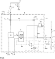
- Figure 1 schematically illustrates one example of a power converter circuit.
- This power converter circuit is configured to receive an input voltage V IN and an input current I IN at an input having a first input node 11 and a second input node 12 and to provide an output voltage V OUT and an output current I OUT at an output 13, 14.
- the power converter may be configured to regulate an output parameter such as the output voltage V OUT , the output current I OUT , or an output power (which is given by the output voltage V OUT multiplied by the output current I OUT ) such that the output parameter has a predefined value.
- the power converter includes a switching circuit 2 connected to the input 11, 12 and a rectifier circuit 3 connected between the switching stage 2 and the output 13, 14.
- the switching circuit 2 includes an electronic switch 22 and an inductor 21 coupled to the electronic switch 22.
- the electronic switch 22 is controlled by a drive signal S DRV received at a drive input of the electronic switch 22 such that the electronic switch 22 switches on or off dependent on the drive signal S DRV .
- the inductor 21 is connected in series with a load path of the electronic switch 22 so that the same current I2 flows through the electronic switch 22 and the inductor 21.
- the electronic switch 22 is configured to conduct a current when the drive signal S DRV switches on the electronic switch 22 (so that the electronic 22 is in an on-state) and is configured to block when the drive signal S DRV switches off the electronic switch 22 (so that the electronic switch 22 is in an off-state).
- Any type of electronic switch such as a MOSFET (Metal Oxide Semiconductor Field-Effect Transistor), an IGBT (Insulated Gate Bipolar Transistor), a HEMT (High Electron-Mobility Transistor), or the like, may be used to implement electronic switch 22.
- the power converter further includes an auxiliary winding 23.
- the auxiliary winding is magnetically coupled to the inductor 21, so that a voltage V AUX across the auxiliary winding 23 is essentially proportional to a voltage V21 across the inductor 21, wherein a proportionality factor between the auxiliary voltage V AUX and the voltage V21 across the inductor 21 is dependent on a ratio between a number of turns of the auxiliary winding 23 and a number of turns of the inductor 21.
- the switching circuit 2 may include further circuit elements and may be coupled to the rectifier circuit 3 in various ways. Different examples are explained herein further below.
- the inductor 21 is coupled to the rectifier circuit 3 in such a way that in a certain operating states of the power converter the voltage V21 across the inductor 21 is representative of the output voltage V OUT .
- the auxiliary voltage V AUX is representative of the output voltage V OUT .
- the operating state in which the voltage V21 across the inductor 21 is representative of the output voltage V OUT is an operating state of the power converter in which the electronic switch 22 is switched off (that is, the electronic switch is in an off-state).
- the power converter further includes a feedback circuit 51.
- the feedback circuit 51 receives an output signal S OUT that represents the output parameter that is to be regulated. That is, the output signal S OUT may represent the output voltage V OUT , the output current I OUT , or the output power P OUT . According to one example, the output signal S OUT represents the output voltage V OUT and is essentially proportional to the output voltage V OUT . According to another example the output signal S OUT represents the output current I OUT and is essentially proportional to the output current I OUT .
- the output signal S OUT may be obtained by measuring the respective output parameter in a conventional way using any kind of voltage, current or power measurement circuit. Such circuits are commonly known, so that no further explanation is required in this regard.
- the feedback circuit 51 is configured to generate a feedback signal S FB based on the output signal S OUT .
- a drive circuit 4 receives the feedback signal S FB at a first input 41 and is configured to generate the drive signal S DRV at an output 40 based on the feedback signal S FB .
- a load Z (illustrated in dashed lines) connected to the output 13, 14 may receive the output voltage V OUT and the output current I OUT .
- the regulated output parameter such as the output voltage V OUT or the output current I OUT , may vary.
- the feedback circuit 51 is configured to generate the feedback signal S FB in such a way that the feedback signal S FB - based on which the electronic switch 22 is driven - counteracts such variations of the regulated output parameter. More specifically, the feedback signal is generated in such a way that, in a steady state of the power converter, the input power, which is controlled by the switched-mode operation of the electronic switch 22, essentially equals the output power received by the load Z.
- the feedback circuit 51 and the drive circuit 4 form a control loop that is configured to regulate the output parameter.
- Regulating the output parameter may include regulating the output parameter such that the output parameter has a predefined value (level).
- the feedback circuit 51 compares the output signal S OUT with a reference signal that represents the predefined value, calculates an error signal based on comparing the output signal S OUT with the reference signal, and generates the feedback signal S FB based on the error signal.
- Generating the feedback signal S FB based on the error signal S ERR may include filtering the error signal S ERR using a filter with any one of a proportional (P) characteristic, an integral (I) characteristic, a proportional-integral (PI) characteristic or a proportional-integrative, derivative (PID) characteristic.
- the switching circuit 2 and the rectifier circuit 3 may be coupled in such way that the input voltage V IN and the output voltage V OUT are referenced to the same ground potential.
- the switching circuit 2 and the rectifier circuit 3 provide for a galvanic isolation between the input 11, 12 and the output 13, 14.
- the power converter may further include a coupler 52 connected between the feedback circuit 51 and the drive circuit 4. This coupler 52 is configured to transmit the feedback signal S FB from the feedback circuit 51 via the galvanic isolation to the drive circuit 4.
- the coupler 52 may include an optocoupler, an inductive coupler, a capacitive coupler, or the like.
- the power converter may be configured in such a way and may be operated in such a way that the auxiliary voltage V AUX in certain operating states of the power converter represents the output voltage V OUT .
- the output voltage V OUT may vary dependent on a power consumption of the load Z, wherein the control loop counteracts such variations of the output voltage V OUT .
- the output voltage V OUT may increase in an uncontrolled fashion.
- the auxiliary voltage V AUX is used to detect an overvoltage at the output 13, 14 in order to be able to promptly react on such overvoltage.
- a voltage V ZCD derived from the auxiliary voltage V AUX is used to detect an overvoltage at the output.
- This voltage V ZCD is referred to as crossing detection voltage in the following, because this voltage V ZCD may further be used to detect time instances when a voltage V21 across the inductor 21 crosses a certain threshold, such as zero. This is explained in detail herein further below.
- the crossing detection voltage V ZCD may be a voltage that is referenced to the same circuit node as the auxiliary voltage V AUX .
- this circuit node is the second input node 12.
- This second input node is also referred to a ground GND node in the following.
- FIG. 2 A block diagram of a method for driving the electronic switch 22 based on the feedback signal S FB and the crossing detection voltage V ZCD , and detecting an overvoltage at the output 13, 14 based on the crossing detection voltage V ZCD , is illustrated in Figure 2 .
- the method includes driving an electronic switch, such as the electronic switch 22 shown in Figure 1 , in a power converter based on a feedback signal, such as the feedback signal S FB shown in Figure 1 , and a crossing detection voltage, such as the crossing detection voltage V ZCD shown in Figure 1 (101).
- the method further includes clamping the crossing detection voltage (102), monitoring a current associated with clamping the crossing detection voltage (103), and detecting an overvoltage scenario based on the monitored current.
- This monitored current is also referred to as auxiliary current or crossing detection current in the following.
- Figure 3 illustrates one example of a drive circuit 4 that is configured to drive the electronic switch 22 in the way explained with reference to Figure 2 .
- the block diagram illustrated in Figure 3 illustrates functional blocks of the drive circuit 4 rather than a specific implementation. Those functional blocks can be implemented in various ways. According to one example, these functional blocks are implemented using dedicated circuits, wherein these circuits may include analog circuits, digital circuits, or mixed circuits including analog and digital circuits.
- the drive circuit 4 is implemented using hardware and software.
- the drive circuit 4 may include a microcontroller and software executed by the microcontroller.
- the drive circuit 4 includes a crossing detection circuit 6.
- the crossing detection circuit 6 is configured to receive the crossing detection voltage V ZCD via the second input 42 of the drive circuit 4 and is configured to clamp the crossing detection voltage V ZCD . Further, the crossing detection circuit 6 is configured to compare the crossing detection voltage V ZCD with a first reference voltage V REF1 in order to detect time periods in which the crossing detection voltage V ZCD crosses the first reference voltage V REF1 .
- the crossing detection circuit 6 includes a voltage limiter 61, and, for comparing the crossing detection voltage V ZCD with the first reference voltage V REF1 , the crossing detection circuit 6 includes a comparator 62.
- a crossing detection signal S ZCD output by the comparator 62 represents those time instances at which the crossing detection voltage V ZCD crosses the first reference voltage V REF1 . More specifically, the crossing detection signal S ZCD may be generated by the crossing detection circuit 6 in such a way that rising and falling edges of the crossing detection signal S ZCD occur each time the crossing detection voltage V ZCD crosses the first reference voltage V REF1 , wherein one of a rising edge and a falling edge occurs when the crossing detection voltage V ZCD crosses the first reference voltage V REF1 in a first direction and the other one of the rising edge and the falling edge occurs when the crossing detection voltage V ZCD crosses the first reference voltage V REF1 in the opposite direction.
- the reference voltage V REF1 is provided by a reference voltage source 63.
- the first reference voltage V REF1 is zero so that the crossing detection signal S ZCD represents those time instances at which the crossing detection voltage V ZCD crosses zero.
- the crossing detection signal S ZCD may be referred to as zero crossing detection signal.
- the voltage source 63 may be omitted.
- a resistor 24 may be connected between the auxiliary winding 23 and the crossing detection circuit 6, so that the crossing detection voltage V ZCD is given by the auxiliary voltage V AUX minus a voltage V24 across the resistor 24. Due to voltage limiter 61 the crossing detection voltage V ZCD is not proportional to the auxiliary voltage V AUX . However, the crossing detection voltage V ZCD turns zero each time the auxiliary voltage V AUX turns zero. Thus, the crossing detection voltage V ZCD can be used to detect time instances when the auxiliary voltage V AUX crosses zero.
- an auxiliary current I AUX flows through the voltage limiter 61.
- the auxiliary current I AUX increases as the auxiliary voltage V AUX increases, wherein, as outlined above, the auxiliary voltage V AUX may be representative of the output voltage V OUT in certain operating states.
- the auxiliary current I AUX is suitable to detect an overvoltage at the output 13, 14.
- a monitoring circuit 7 monitors the auxiliary current I AUX and outputs an overvoltage signal S OV based on monitoring the auxiliary current I AUX .
- the overvoltage signal S OV may have one of two different signal levels, (a) a first signal level, which is referred to as fault level in the following, indicates that an overvoltage has been detected, and (b) a second signal level, which may be referred to as normal level in the following, indicates that an overvoltage has not been detected.
- the monitoring circuit 7 may include a current sensor 71 that is configured to measure the auxiliary current I AUX and provide a current measurement signal S71 that represents the auxiliary current I AUX .
- the monitoring circuit 7 may include an evaluation circuit 72 that receives the current measurement signal S71 and generates the overvoltage signal S OV based on comparing the current measurement signal S71 with a reference signal.
- the drive circuit 4 may further include a drive signal generator 8 that receives the crossing detection signal S ZCD and the feedback signal S FB and that generates the drive signal S DRV based on these signals.
- the drive signal generator 8 may further receive the overvoltage signal S OV in order to drive the electronic switch 22 based on the overvoltage signal S OV in addition to the crossing detection signal S ZCD and the feedback signal S FB .
- FIG 4 schematically illustrates a timing diagram of the drive signal S DRV generated by the drive circuit 4.
- the drive signal S DRV includes a plurality of successive drive periods. Each drive period includes an on-period in which the drive signal S DRV has an on-level that switches on the electronic switch 22, and an off-period in which the drive signal S DRV has an off-level that switches off the electronic switch 22.
- the on-level is a high signal level in the example illustrated in Figure 4
- the off-level is a low signal level of the drive signal S DRV .
- the drive circuit 4 may be configured to vary at least one of a duration T ON of the on-period in the individual drive cycles and a duration T OFF of the off-period of the individual drive cycles in order to regulate the output parameter.
- the switching circuit 2 may be implemented in such a way that energy is stored in the inductor 21 in each on-period and that the stored energy is transferred to the rectifier circuit 3 in each off-period.
- Figure 5 illustrates a modification of the drive circuit 4 shown in Figure 3 .
- the drive circuit 4 according to Figure 5 is further configured to monitor the current I2 through the electronic switch 22 by monitoring a voltage V91 across a first resistor 91 connected in series with the electronic switch 22.
- a load current monitoring circuit 9 is configured to compare the voltage V91 across the first resistor 91 with a second reference voltage V REF2 provided by a reference voltage source 93 and to generate an overcurrent signal S OC based on comparing the voltage V91 across the first resistor 91 with the second reference voltage V REF2 .
- a comparator 92 compares the voltage V91 across the first resistor 91 with the second reference voltage V REF2 and outputs the overcurrent signal S OC .
- the overcurrent signal S OC either has a first level, which is referred to as overcurrent level in the following, and a second level, which is referred to as normal level in the following.
- the comparator 92 is configured to generate the overcurrent level of the overcurrent signal S OC when the voltage V91 across the first resistor 91 is higher than the second reference voltage V REF2 .
- the drive signal generator 8 receives the overcurrent signal S OC and may be configured to immediately switch off the electronic switch 22 when the overcurrent signal S OC indicates that an overcurrent scenario has occurred.
- the evaluation circuit 72 of the auxiliary current monitoring circuit 7 includes a second resistor 711 that is connected between a first circuit node 43 and the first resistor 91. More specifically, the second resistor 711 is connected between the first circuit node 43 and a circuit node at which the first resistor 91 can be connected to the electronic switch 22. Further, the evaluation circuit 72 includes a controlled current source 721 that receives the current measurement signal S71 and is configured to drive a current I AUX2 via the first circuit node 43 through the second resistor 711 and the first resistor 91 when the electronic switch 22 is in the off-state. According to one example, this current I AUX2 is proportional to the auxiliary current I AUX and is therefore referred to as further auxiliary current I AUX2 in the following.
- a resistance R711 of the second resistor 711 is significantly higher than a resistance R91 of the first resistor 91. According to one example, a ratio R711/R91 between these resistances is greater than 1000 (1E3) or greater than 10000 (1E4).
- the resistance R711 of the second resistor 711 is between 1 kiloohm (k ⁇ ) and 10 k ⁇ , for example, and the resistance R91 of the first resistor 91 is between 0.1 ohms ( ⁇ ) and 1 ⁇ , for example.
- a voltage V43 at the first circuit node 43 that is, a voltage across a series circuit including the first resistor 91 and the second resistor 711 is given by a voltage V91 across the first resistor 91 plus a voltage V711 across the second resistor 711.
- the current I2 through the electronic switch 22 is zero so that the voltage V43 at the first circuit node 43 is only dependent on the further auxiliary current I AUX2 .
- the comparator 91 has a high input impedance so that the further auxiliary current I AUX2 essentially only flows through the two resistors 91, 711).
- the evaluation circuit 72 is configured to compare the voltage V43 at the first circuit node 43 with a third reference voltage V REF3 provided by a reference voltage source 724 and output the overvoltage signal S OV . More specifically, a comparator 723 compares the input voltage V43 with the third reference voltage V REF3 and outputs the overvoltage signal S OV .
- the signal level of the auxiliary current I AUX at which an overvoltage level of the overvoltage signal S OV is generated can be adjusted by suitably adjusting a ratio between the auxiliary current I AUX and the further current auxiliary current I AUX2 and by suitably selecting a resistance of the second resistor 711.
- the drive circuit 4 may include an integrated circuit IC wherein the voltage limiter 6 and the drive signal generator 8 may be integrated in the integrated circuit IC. Further, the monitoring circuit 7 except for the second resistor 711 and the load current monitoring circuit 9 except for the first resistor 91 may be integrated in the integrated circuit IC. Thus, the first resistor 91 and the second resistor 72 may be discrete devices externally connected to the integrated circuit IC.
- the first and second inputs 41, 42 and the supply inputs 44, 45 of the drive circuit 4 may be formed by respective input pins of the integrated circuit IC and the output 40 may be formed by an output pin of the integrated circuit IC. Further, the first circuit node 43 may be formed by a further input pin of the integrated circuit IC.
- the same input pin of the integrated circuit IC can be used, so that for the overcurrent detection, which uses the first resistor 91, and the overvoltage detection, which uses the first resistor 91 and the second resistor 92, the same input pin can be used.
- each additional input pin (or output pin) is associated with additional costs.
- the monitoring circuit 7 is configured to generate the further auxiliary current I AUX2 only when the auxiliary voltage V AUX has a certain polarity that only occurs when the electronic switch 22 is in the off-state.
- the voltage V43 received at the first circuit node 43 equals the voltage V91 across the first resistor 91, because in this operating state the further auxiliary current I AUX2 and, therefore, the voltage V711 across the second resistor 711 is zero.
- the current I2 through the electronic switch 22 is zero.
- the input voltage V43 at the third input 43 is only given by the further auxiliary current I AUX2 and by resistances R711, R91 of the first and second resistor 711, 91.
- the overvoltage signal S OV is not the output signal of the comparator 723, but is generated by an evaluation circuit 725 based on the comparator output signal.
- the evaluation circuit 725 may be configured to generate the overvoltage level of the overvoltage signal S OV only when the comparator output signal indicates that the input voltage V43 at the first circuit node 43 is higher than the third reference voltage V REF3 longer than a predefined time period. In this way, voltage spikes of the auxiliary voltage V AUX and, therefore, current spikes of the auxiliary current I AUX that may occur in transition phases of the electronic switch 22 from the on-state to the off-state, or vice versa, do not result in an erroneous detection of an overvoltage scenario.
- the evaluation circuit 725 may be configured to generate the overvoltage level of the overvoltage signal S OV only when the voltage V43 at the first circuit node 43 is higher than the third reference voltage V REF3 in a predefined number of successive drive cycles of the electronic switch 22.
- the evaluation circuit 725 may be configured to generate an overvoltage level of the overvoltage signal S OV only generated when the input voltage V43 is higher than the third reference voltage V REF3 for longer than the predefined time period in each of a predefined number of successive drive cycles.
- the evaluation circuit 725 may receive the drive signal S DRV in order to be able to detect when a new drive cycle starts.
- the drive circuit 4 may further receive a supply voltage VDD between supply nodes 44, 45, wherein one of these supply nodes may be connected to the ground node GND.
- the supply voltage VDD supplies the individual circuit blocks in the drive circuit 4.
- the drive voltage VDD may be generated based on the auxiliary voltage V AUX using a rectifier circuit 25, that may include rectifier element 251 and a capacitor 252.
- generating the supply voltage VDD based on the auxiliary voltage V AUX is only an example.
- a further auxiliary winding coupled to the inductor 21 may be used to generate the supply voltage VDD.
- Figure 6 illustrates a modification of the drive circuit shown in Figure 5 .
- the voltage V43 at the third input is only compared with the second reference voltage V REF2 .
- the output signal of the comparator 92 is used for both overcurrent and overvoltage detection purposes. More specifically, the output signal of the comparator 92 is the overcurrent signal S OC when the electronic switch 22 is in the on-state, and the output signal of the comparator 92 is processed by the evaluation circuit 725 in order to generate the overvoltage signal S OV when the electronic switch 22 is in the off-state.
- Figure 7 illustrates one example of the voltage limiter 61, the current sensor 71 and the current source 721 in greater detail.
- the voltage limiter 61 includes a first transistor N1 connected between the second input node 42 and the ground node 44 of the drive circuit 4.
- the first transistor N1 clamps the crossing detection voltage V ZCD .
- Driving the first transistor N1 in an on-state so that it clamps the crossing detection voltage V ZCD is explained in detail herein further below.
- the voltage limiter 61 further includes a second transistor N2 connected between a first circuit node M1 and the ground node 12, and a third transistor N3 connected between the first circuit node M1 and the second input node 42. Further, a current regulator is configured to control a current I M1 into the first circuit node M1 in two different ways dependent on a polarity of the auxiliary voltage V AUX . The current I M1 into the first circuit node is provided from a supply node M3 where the supply voltage VDD is available.
- the regulator controls the current I M1 into the first circuit node M1 such that the first transistor N1 and the second transistor N2 are operated in the same operating point and a current I N3 through the third transistor N3 is zero.
- a current level of a current I N2 through the second transistor N2 is proportional to a current I N1 through the first transistor N1, wherein the current I N1 through the first transistor N1 equals the auxiliary current I AUX .
- the first transistor N1 and the second transistor N2 have the same length and the same width. In this case, the current I N2 through the second transistor N2 and the auxiliary current I AUX have the same current level.
- the regulator includes an operational amplifier OP1 that has a first input connected to the first circuit node M1 and second input connected to a second circuit node M2.
- a switch S2 that is controlled by a comparator K1 connects the second circuit node M2 to the second input 42 when the auxiliary voltage V AUX has the first polarity.
- the operational amplifier OP1 controls the current I M1 into the first circuit node M1 such that the potential at the first circuit node M1 equals the potential at the second input 42, so that a voltage across the third transistor N3 is zero.
- the current I N3 through the third transistor N3 is zero.
- the regulator further includes a variable resistor N7 driven by the operational amplifier 0P1 and connected between the supply node M3 and the ground node 12, and a current mirror P1, P2.
- the variable resistor N7 includes a transistor driven by the operational amplifier.
- a filter R, C is connected between an output of the operational amplifier OP1 and the transistor of the variable resistor N7.
- the current mirror P1, P2 is configured to mirror a current I N7 through the variable resistor N7 such that the current I M1 into the first circuit node M1 is proportional to the current I N7 through the variable resistor N7, wherein a proportionality factor between the current through the variable resistor N7 and the current I M1 into the first circuit node M1 is given by a current mirror ratio of the current mirror.
- the current mirror ratio is 1:1, so that the current I M1 into the first circuit M1 equals the current I N7 through the variable resistor N7.
- the regulator via the variable resistor N7 and the current mirror P1, P2, adjusts the current I M1 into the first circuit node M1 such that the current I N3 through the third transistor N3 is zero, so that - in a steady state of the regulator - the current I M1 into the first circuit node M1 equals the current I N2 through the second transistor N2, wherein the latter is proportional to the auxiliary current I AUX .
- the current through the variable resistor N7 is proportional to the auxiliary current I AUX .
- This current I N7 through the variable resistor N7 represents the current measurement signal S71 mentioned above.
- the voltage limiter 61 further includes a further transistor N5 connected between an output transistor P2 of the current mirror P1, P2 and the first circuit node M1.
- This further transistor N5 is connected as a diode. That is, a drain node of the further transistor N5 is connected to its gate node.
- gate nodes of the first, second and third transistors N1, N2, N3 are connected to the drain/gate node of the further transistor, so that these transistors N1, N2, N3 have the same electrical potential at their respective gate node.
- the first transistor N1 and the second transistor N2 are activated, so that they may conduct a current, as soon as the potential at their respective gate node reaches a level at which gate-source voltage of these transistors N1, N2 becomes higher than the respective threshold voltages.
- the first, second and third transistor N1-N3 have the same threshold voltage.
- the threshold voltage of the fifth transistor N5 may be lower than the threshold voltages of the first, second and third transistor N1, N2, N3.
- the clamping voltage which is the voltage level at which the crossing detection voltage V ZCD is clamped by the voltage limiter 61, is predefined, but not fixed.
- This clamping voltage is defined by the characteristic curve of the first transistor N1 and is dependent on a current level of the auxiliary current I AUX .
- the clamping voltage is predefined by the first transistor N1, but not fixed.
- the higher the auxiliary current I AUX the higher the clamping voltage.
- there is a square relationship between the clamping voltage and the auxiliary current I AUX so that variations of the clamping voltage dependent on the auxiliary current I AUX are essentially negligible.
- the first transistor N1 is implemented such that a voltage drop across the first transistor N1 is less than 5% or even less than 2% of the auxiliary voltage V AUX during the demagnetization phase.
- a magnitude of the crossing detection voltage V ZCD is almost negligible compared to the magnitude of the auxiliary voltage V AUX , so that in each case the auxiliary current I AUX is essentially proportional to the auxiliary voltage V AUX .
- the current sensor 71 includes a further transistor N6 that is coupled to the variable resistor N7 and the current source 721 includes a further current mirror P3, P4 that is configured to generate the further auxiliary current I AUX2 such that the further auxiliary current I AUX2 is proportional to the current I N7 through the variable resistor N7.
- the further current mirror may include a switch S4 controlled by the comparator K1, wherein the comparator K1 may be configured to close this switch S4 only when the crossing detection voltage V ZCD has the first polarity, so that the further auxiliary current I AUX2 is only provided when the electronic switch 22 is in the off-state.
- the switch S2 controlled by the comparator K1 connects the second circuit node M2 to the ground node 44.
- the operational amplifier OP1 controls the current I M1 into the first circuit node M1 such that the potential at the first circuit node M1 equals the potential at the ground node 44.
- the voltage across the second transistor N2 is zero and the voltage across the third transistor N3 equals the crossing detection voltage V ZCD .
- the current I N2 through the second transistor N2 is zero and the third transistor N3 is operated in the same operating point as the first transistor N1, so that the current IN3 through the third transistor N3 is proportional to the current I N1 through the first transistor N1.
- the further auxiliary current is zero because the switch S4 in the current source 721 is switched off by the comparator.
- the power converter has a flyback topology.
- the inductor 21 is a transformer with a primary winding 21 1 and a secondary winding 21 2 .
- the primary winding 21 1 is connected in series with the electronic switch 22, wherein the series circuit with the primary winding 21 1 and the electronic switch 22 is connected between a first node 11 and a second node 12 of the input 11, 12.
- the secondary winding 21 2 is connected to the rectifier circuit 3.
- the rectifier 3 includes a rectifier element 31, such as a diode, and a capacitor 32, wherein the output voltage V OUT is available across the capacitor 32.
- Figure 9 shows timing diagrams that illustrate the current I2 through the electronic switch 22, the current I3 through the rectifier circuit 3, the voltage V21 1 across the primary winding of the transformer 21, the auxiliary voltage V AUX , the crossing detection voltage V ZCD , the crossing detection signal S ZCD , the voltage V22 across the electronic switch 22, and the drive signal S DRV in one drive cycle of the power converter.
- the electronic switch 22 When the electronic switch 22 is in the on-state, that is, during the on-period T ON , the current through the primary winding 21 1 and the electronic switch 22 increases (wherein an increase of the current I2 is essentially proportional to the input voltage V IN and inversely proportional to an inductance of the transformer 21).
- the voltage V21 1 across the primary winding 21 1 essentially equals the input voltage V IN .
- the voltage V21 1 across the primary winding 21 1 is also referred to as primary voltage in the following.
- the primary winding 21 1 and the auxiliary winding 23 have opposite winding senses.
- the auxiliary voltage V AUX has a polarity that is opposite the polarity of the voltage across the primary winding 21 1 .
- the auxiliary voltage V AUX is negative during the on-period T ON .
- the auxiliary voltage V AUX is proportional to the input voltage V IN during the on-period. A proportionality factor is given by a ratio between the number of turns of the auxiliary winding 23 and a number of turns of the primary winding 21 1 .
- the crossing detection voltage V ZCD follows the auxiliary voltage V AUX , but has its magnitude limited by the voltage limiter explained above.
- the current I2 through the primary winding 21 1 rapidly decreases to zero and the energy previously stored in the transformer 21 during the on-period induces a secondary current I3 through the secondary winding 21 2 , wherein this current I3 decreases over time.
- the primary voltage V21 1 and, therefore, the auxiliary voltage V AUX change their respective polarity. That is, in the example shown in Figure 9 , the primary voltage V21 1 turns negative and the auxiliary voltage V AUX turns positive.
- the voltage V22 across the electronic switch 22 is given by the input voltage V IN plus the primary voltage V21 1 .
- the voltage V AUX is essentially proportional to the output voltage V OUT during the demagnetization period. Further, as explained above, the auxiliary current I AUX that occurs by clamping the crossing detection voltage V ZCD is dependent on the auxiliary voltage V AUX such that the auxiliary current I AUX increases as the auxiliary voltage V AUX increases.
- the voltage limiter 61 is configured to limit (clamp) the crossing detection voltage V ZCD to a voltage of below 500 millivolts (mV) or even below 300 mV and the auxiliary winding 23 is implemented in such a way that the auxiliary voltage V AUX during the demagnetization period is higher than 10V or higher than 15V (when there is no overvoltage at the output 13, 14).
- a magnitude of the crossing detection voltage V ZCD is almost negligible compared to the magnitude of the auxiliary voltage V AUX , so that the auxiliary current I AUX is essentially proportional to the auxiliary voltage V AUX .
- the crossing detection circuit 6 may be configured in such a way that the crossing detection voltage V ZCD is clamped even when the power converter is in a normal operating mode, that is, when no overvoltage at the output 13, 14 occurs.
- the magnitude of the primary voltage V21 1 , the auxiliary voltage V AUX , and the voltage V22 across the switch 22 decreases, wherein the electronic switch 22 is again switched on after the transformer 21 has been demagnetized in order to start a new drive cycle.
- the first reference voltage V REF1 in the crossing detection circuit 6 is zero.
- the crossing detection signal S ZCD changes its polarity each time the auxiliary voltage V AUX changes its polarity.
- the crossing detection signal S ZCD changes its polarity when the primary voltage V21 1 and the auxiliary voltage V AUX turns zero.
- the auxiliary voltage V AUX changes its polarity from positive to negative at the end of the demagnetization period so that the crossing detection signal S ZCD has a falling edge at the end of the demagnetization period.
- each edge of the crossing detection signal S ZCD indicates that the auxiliary voltage crosses the first reference voltage V REF1 (such as zero).
- the drive circuit 4 may be configured to again switch on the electronic switch 22 as soon as the crossing detection signal S ZCD indicates that the transformer has demagnetized.
- the drive circuit 4 it is also possible for the drive circuit 4 to wait a certain time period after the transformer has been demagnetized before again switching on the electronic switch 22. In this case, oscillations of the primary voltage V21 1 , the auxiliary voltage V AUX and the voltage V22 across the electronic switch 22 may occur. Referring to Figure 9 , the voltage V22 across the electronic switch 22 regularly reaches a minimum after the transformer has been demagnetized. According to one example, the drive circuit 4 is configured to switch on the electronic switch 22 at one of those time instances at which the voltage V22 reaches a minimum.
- a voltage minimum of the voltage V22 essentially occurs a quarter (1/4) of the oscillation period after the auxiliary voltage V AUX crosses zero in a certain direction.
- a minimum of the voltage V22 occurs each time after the auxiliary voltage V AUX turns negative, that is, after a falling edge of the crossing detection signal S ZCD occurs.
- the "oscillation period” is the period of the voltage oscillations that occur during the waiting time. This period, inter alia, is dependent on an inductance of the transformer 21 and parasitic capacitances such as a capacitance of the electronic switch 22.
- FIG 10 shows one example of the drive signal generator 8 in greater detail.
- this drive signal generator 8 includes a controller 81 that receives the feedback signal S FB and that optionally receives the overcurrent signal S OC and the overvoltage signal S OV .
- a counter 82 receives the crossing detection signal S ZCD and a reference signal S ZCD_REF from the controller 81. This counter 82 is reset by the drive signal S DRV at the beginning of each drive cycle and is configured to count predefined edges, such as falling edges, of the crossing detection signal S ZCD .
- the counter 82 is configured to cause an on-level of the drive signal S DRV by setting a flip-flop 83 each time the number of detected edges of the crossing detection signal S ZCD reaches the reference value S ZCD_REF provided by the controller 81.
- the controller 81 is configured to adjust the reference value S ZCD_REF dependent on the feedback signal S FB received from the feedback circuit 51.
- a delay element 86 between the counter 82 and the flip-flop 83. This delay element 86 may provide for a delay that is given by one quarter of the oscillation period, so that the flip-flop 83 is set (and the electronic switch 22 switches on) one quarter of the oscillation period after the predefined edge of the crossing detection signal S ZCD .
- the controller 81 is further configured to adjust the duration of the on-period based on the feedback signal S FB .
- a further delay element 84 receives an on-period signal S TON that defines the duration of the on-period from the controller 81.
- This delay element 84 is connected to a reset input of the flip-flop 83 and further receives the counter signal S CTR .
- This delay element 84 ensures that the flip-flop 83 is reset after a time period defined by S TON after the flip-flop 83 has been set.
- the controller 81 may be configured to increase the reference signal S ZCD_REF as the feedback signal S FB indicates that the power consumption of the load Z decreases. Further, at a given reference signal S ZCD_REF , the controller 81 may be configured to reduce the duration T ON of the on-periods as the power consumption of the load Z decreases. In other words, the lower the power consumption of the load Z, the higher the value represented by the reference signal S ZCD_REF and/or the shorter the on-periods.
- the controller 81 receives at least one of the overcurrent signal S OC and the overvoltage signal S OV and is configured to generate an error signal S ER-ROR based on the at least one of these signals S OC , S OV .
- a logic gate 85 such as an OR gate, is optional and receives the error signal S ERROR and the output signal of the delay element 84. This logic element 85 is configured to reset the flip-flop 83 either when an output signal of the delay element 84 indicates that the flip-flop 83 is to be reset in order to end the on-period or when the error signal S ERROR indicates that an error has occurred.
- another logic gate 87 that receives the error signal S ERROR and the counter signal S CTR is connected between the counter 82 and the flip-flop 83.
- This logic gate is configured to prevent the flip-flop 83 from being set when the error signal S ER-ROR indicates that an error has occurred. In this way, as soon as an error occurs, the on-period may be interrupted and further on-periods are prevented.
- the controller 81 may generate the error signal S ERROR based on the overcurrent signal S OV and the overvoltage signal S OV in different ways.
- the overcurrent signal S OC indicates an overcurrent the controller 81 may be configured to generate the error signal S ERROR such that it has an error signal for a short time period that causes the flip-flop 83 to be reset, but does not prevent a further switched-mode operation of the power converter.
- the overvoltage signal S OV indicates an error
- the controller 81 may generate an error level of the error signal S ERROR for a time period that is long enough to interrupt the switched-mode operation of the power converter for a certain time period.
- the controller 81 may reset the error signal S ERROR after a certain period.
- the error signal S ERROR is only reset after the drive circuit 4 has been reset. "Resetting" the drive circuit 4 may include interrupting the supply voltage VDD of the drive circuit 4.
Landscapes
- Engineering & Computer Science (AREA)
- Power Engineering (AREA)
- Dc-Dc Converters (AREA)
Priority Applications (2)
| Application Number | Priority Date | Filing Date | Title |
|---|---|---|---|
| EP19177203.7A EP3745593A1 (de) | 2019-05-29 | 2019-05-29 | Verfahren zur ansteuerung eines schalter in einem stromwandler, ansteuerungsschaltung und stromwandler |
| US16/860,475 US11616445B2 (en) | 2019-05-29 | 2020-04-28 | Method for driving a switch in a power converter, drive circuit and power converter |
Applications Claiming Priority (1)
| Application Number | Priority Date | Filing Date | Title |
|---|---|---|---|
| EP19177203.7A EP3745593A1 (de) | 2019-05-29 | 2019-05-29 | Verfahren zur ansteuerung eines schalter in einem stromwandler, ansteuerungsschaltung und stromwandler |
Publications (1)
| Publication Number | Publication Date |
|---|---|
| EP3745593A1 true EP3745593A1 (de) | 2020-12-02 |
Family
ID=66676328
Family Applications (1)
| Application Number | Title | Priority Date | Filing Date |
|---|---|---|---|
| EP19177203.7A Pending EP3745593A1 (de) | 2019-05-29 | 2019-05-29 | Verfahren zur ansteuerung eines schalter in einem stromwandler, ansteuerungsschaltung und stromwandler |
Country Status (2)
| Country | Link |
|---|---|
| US (1) | US11616445B2 (de) |
| EP (1) | EP3745593A1 (de) |
Families Citing this family (3)
| Publication number | Priority date | Publication date | Assignee | Title |
|---|---|---|---|---|
| EP3758204A1 (de) * | 2019-06-28 | 2020-12-30 | Infineon Technologies Austria AG | Verfahren zur ansteuerung einer elektronischen schaltung in einem stromwandlerkreislauf sowie stromwandlerkreislauf |
| EP3761494A1 (de) | 2019-07-02 | 2021-01-06 | Infineon Technologies Austria AG | Verfahren zur ansteuerung einer elektronischen schaltung in einem stromwandlerkreislauf sowie stromwandlerkreislauf |
| TWI711248B (zh) * | 2020-04-17 | 2020-11-21 | 通嘉科技股份有限公司 | 應用於電源轉換器的一次側的初級控制器及其操作方法 |
Citations (2)
| Publication number | Priority date | Publication date | Assignee | Title |
|---|---|---|---|---|
| US20150043252A1 (en) * | 2013-08-09 | 2015-02-12 | Chengdu Monolithic Power Systems Co., Ltd. | Switching mode power supply and the control method thereof |
| US20150280575A1 (en) * | 2014-03-31 | 2015-10-01 | Delta Electronics (Shanghai) Co., Ltd. | Control device, control method of power converter and switching power supply |
Family Cites Families (9)
| Publication number | Priority date | Publication date | Assignee | Title |
|---|---|---|---|---|
| US5784231A (en) * | 1997-04-25 | 1998-07-21 | Philips Electronics North America Corp. | Overvoltage protection for SMPS based on demagnetization signal |
| TW200845529A (en) * | 2007-05-11 | 2008-11-16 | Richtek Technology Corp | An apparatus and method for utilizing an auxiliary coil in an isolation voltage-converter to accomplish multiple functions and protections |
| US8054656B2 (en) * | 2008-04-11 | 2011-11-08 | System General Corp. | Switching control circuit for a switching power converter |
| KR101745704B1 (ko) * | 2009-10-26 | 2017-06-12 | 페어차일드코리아반도체 주식회사 | 역률 보상 회로 및 역률 보상 회로의 구동 방법 |
| TWI403078B (zh) * | 2009-12-16 | 2013-07-21 | Leadtrend Tech Corp | 適用於開關式電源供應器之開關控制器及其方法 |
| TWI487255B (zh) * | 2012-07-13 | 2015-06-01 | Power Forest Technology Corp | 以反馳式架構為基礎的電源轉換裝置及其電源轉換方法 |
| CN104660022B (zh) * | 2015-02-02 | 2017-06-13 | 昂宝电子(上海)有限公司 | 为电源变换器提供过流保护的系统和方法 |
| TWI671982B (zh) * | 2017-10-03 | 2019-09-11 | 偉詮電子股份有限公司 | 可提供不同保護之電源轉換器、電源控制器、以及相關之控制方法 |
| CN109742964A (zh) * | 2018-12-28 | 2019-05-10 | 成都芯源系统有限公司 | 具有输入功率限制的ac/dc变换器的控制电路和方法 |
-
2019
- 2019-05-29 EP EP19177203.7A patent/EP3745593A1/de active Pending
-
2020
- 2020-04-28 US US16/860,475 patent/US11616445B2/en active Active
Patent Citations (2)
| Publication number | Priority date | Publication date | Assignee | Title |
|---|---|---|---|---|
| US20150043252A1 (en) * | 2013-08-09 | 2015-02-12 | Chengdu Monolithic Power Systems Co., Ltd. | Switching mode power supply and the control method thereof |
| US20150280575A1 (en) * | 2014-03-31 | 2015-10-01 | Delta Electronics (Shanghai) Co., Ltd. | Control device, control method of power converter and switching power supply |
Also Published As
| Publication number | Publication date |
|---|---|
| US20200382005A1 (en) | 2020-12-03 |
| US11616445B2 (en) | 2023-03-28 |
Similar Documents
| Publication | Publication Date | Title |
|---|---|---|
| EP1215808B1 (de) | Stromversorgungsschaltung und dazugehöriges Verfahren zur Entmagnetisierungsdetektion der Stromversorgung | |
| US6665197B2 (en) | Circuit configuration for producing a switching signal for a current-controlled switch-mode power supply | |
| US10491117B2 (en) | Soft-start circuit for buck converter control | |
| US10879811B2 (en) | Switching power supply device and semiconductor device | |
| US8018694B1 (en) | Over-current protection for a power converter | |
| JP5453508B2 (ja) | 効率的軽負荷動作を有する分離フライバックコンバータ | |
| US11601044B2 (en) | Method for driving an electronic switch in a power converter circuit and control circuit | |
| US9948187B2 (en) | System and method for a switched-mode power supply | |
| US9647562B2 (en) | Power conversion with switch turn-off delay time compensation | |
| TW201946351A (zh) | 電源控制用半導體裝置以及開關電源裝置及其設計方法 | |
| US9136767B2 (en) | Switching power-supply device | |
| US8611110B2 (en) | Switching power supply apparatus | |
| KR101365502B1 (ko) | 전원 장치 | |
| US10897194B2 (en) | Power factor improvement circuit and semiconductor apparatus | |
| KR100583670B1 (ko) | 스위칭 전원 장치 | |
| US11616445B2 (en) | Method for driving a switch in a power converter, drive circuit and power converter | |
| US11228242B2 (en) | Power converter and method for driving an electronic switch | |
| JPH06311734A (ja) | 出力短絡保護回路 | |
| WO2012077588A1 (ja) | 絶縁型直流電源装置 | |
| JP2019080433A (ja) | 同期整流回路及びスイッチング電源装置 | |
| US12051964B2 (en) | Current detection circuit including non-linear circuit and power supply circuit containing the same | |
| KR20130044979A (ko) | 전원 공급 장치 | |
| US9054591B2 (en) | Switching power supply apparatus and method of controlling switching power supply apparatus | |
| EP4503412A1 (de) | Stromwandler mit einer erfassungsschaltung und verfahren | |
| GB2578931A (en) | Test apparatus |
Legal Events
| Date | Code | Title | Description |
|---|---|---|---|
| PUAI | Public reference made under article 153(3) epc to a published international application that has entered the european phase |
Free format text: ORIGINAL CODE: 0009012 |
|
| STAA | Information on the status of an ep patent application or granted ep patent |
Free format text: STATUS: THE APPLICATION HAS BEEN PUBLISHED |
|
| AK | Designated contracting states |
Kind code of ref document: A1 Designated state(s): AL AT BE BG CH CY CZ DE DK EE ES FI FR GB GR HR HU IE IS IT LI LT LU LV MC MK MT NL NO PL PT RO RS SE SI SK SM TR |
|
| AX | Request for extension of the european patent |
Extension state: BA ME |
|
| STAA | Information on the status of an ep patent application or granted ep patent |
Free format text: STATUS: REQUEST FOR EXAMINATION WAS MADE |
|
| 17P | Request for examination filed |
Effective date: 20210602 |
|
| RBV | Designated contracting states (corrected) |
Designated state(s): AL AT BE BG CH CY CZ DE DK EE ES FI FR GB GR HR HU IE IS IT LI LT LU LV MC MK MT NL NO PL PT RO RS SE SI SK SM TR |
|
| STAA | Information on the status of an ep patent application or granted ep patent |
Free format text: STATUS: EXAMINATION IS IN PROGRESS |
|
| 17Q | First examination report despatched |
Effective date: 20221031 |
|
| REG | Reference to a national code |
Ref country code: DE Ref legal event code: R079 Free format text: PREVIOUS MAIN CLASS: H03K0017080000 Ipc: H02M0001000000 |
|
| GRAP | Despatch of communication of intention to grant a patent |
Free format text: ORIGINAL CODE: EPIDOSNIGR1 |
|
| STAA | Information on the status of an ep patent application or granted ep patent |
Free format text: STATUS: GRANT OF PATENT IS INTENDED |
|
| RIC1 | Information provided on ipc code assigned before grant |
Ipc: H02M 1/00 20060101AFI20260318BHEP Ipc: H02M 1/32 20070101ALI20260318BHEP Ipc: H02M 3/335 20060101ALI20260318BHEP Ipc: H03K 17/082 20060101ALI20260318BHEP |
|
| INTG | Intention to grant announced |
Effective date: 20260330 |