EP3747088B1 - Connecteur à fiche mâle modulaire ayant une carte de circuit imprimé multicouche pour des applications à très haute vitesse - Google Patents
Connecteur à fiche mâle modulaire ayant une carte de circuit imprimé multicouche pour des applications à très haute vitesse Download PDFInfo
- Publication number
- EP3747088B1 EP3747088B1 EP19705667.4A EP19705667A EP3747088B1 EP 3747088 B1 EP3747088 B1 EP 3747088B1 EP 19705667 A EP19705667 A EP 19705667A EP 3747088 B1 EP3747088 B1 EP 3747088B1
- Authority
- EP
- European Patent Office
- Prior art keywords
- plug
- pcb
- contact
- contacts
- conductive shield
- Prior art date
- Legal status (The legal status is an assumption and is not a legal conclusion. Google has not performed a legal analysis and makes no representation as to the accuracy of the status listed.)
- Active
Links
Images


Classifications
-
- H—ELECTRICITY
- H01—ELECTRIC ELEMENTS
- H01R—ELECTRICALLY-CONDUCTIVE CONNECTIONS; STRUCTURAL ASSOCIATIONS OF A PLURALITY OF MUTUALLY-INSULATED ELECTRICAL CONNECTING ELEMENTS; COUPLING DEVICES; CURRENT COLLECTORS
- H01R24/00—Two-part coupling devices, or either of their cooperating parts, characterised by their overall structure
- H01R24/60—Contacts spaced along planar side wall transverse to longitudinal axis of engagement
- H01R24/62—Sliding engagements with one side only, e.g. modular jack coupling devices
- H01R24/64—Sliding engagements with one side only, e.g. modular jack coupling devices for high frequency, e.g. RJ 45
-
- H—ELECTRICITY
- H01—ELECTRIC ELEMENTS
- H01R—ELECTRICALLY-CONDUCTIVE CONNECTIONS; STRUCTURAL ASSOCIATIONS OF A PLURALITY OF MUTUALLY-INSULATED ELECTRICAL CONNECTING ELEMENTS; COUPLING DEVICES; CURRENT COLLECTORS
- H01R13/00—Details of coupling devices of the kinds covered by groups H01R12/70 or H01R24/00 - H01R33/00
- H01R13/46—Bases; Cases
- H01R13/502—Bases; Cases composed of different pieces
- H01R13/506—Bases; Cases composed of different pieces assembled by snap action of the parts
-
- H—ELECTRICITY
- H01—ELECTRIC ELEMENTS
- H01R—ELECTRICALLY-CONDUCTIVE CONNECTIONS; STRUCTURAL ASSOCIATIONS OF A PLURALITY OF MUTUALLY-INSULATED ELECTRICAL CONNECTING ELEMENTS; COUPLING DEVICES; CURRENT COLLECTORS
- H01R13/00—Details of coupling devices of the kinds covered by groups H01R12/70 or H01R24/00 - H01R33/00
- H01R13/46—Bases; Cases
- H01R13/514—Bases; Cases composed as a modular blocks or assembly, i.e. composed of co-operating parts provided with contact members or holding contact members between them
-
- H—ELECTRICITY
- H01—ELECTRIC ELEMENTS
- H01R—ELECTRICALLY-CONDUCTIVE CONNECTIONS; STRUCTURAL ASSOCIATIONS OF A PLURALITY OF MUTUALLY-INSULATED ELECTRICAL CONNECTING ELEMENTS; COUPLING DEVICES; CURRENT COLLECTORS
- H01R13/00—Details of coupling devices of the kinds covered by groups H01R12/70 or H01R24/00 - H01R33/00
- H01R13/646—Details of coupling devices of the kinds covered by groups H01R12/70 or H01R24/00 - H01R33/00 specially adapted for high-frequency, e.g. structures providing an impedance match or phase match
- H01R13/6461—Means for preventing cross-talk
- H01R13/6464—Means for preventing cross-talk by adding capacitive elements
- H01R13/6466—Means for preventing cross-talk by adding capacitive elements on substrates, e.g. printed circuit boards [PCB]
-
- H—ELECTRICITY
- H01—ELECTRIC ELEMENTS
- H01R—ELECTRICALLY-CONDUCTIVE CONNECTIONS; STRUCTURAL ASSOCIATIONS OF A PLURALITY OF MUTUALLY-INSULATED ELECTRICAL CONNECTING ELEMENTS; COUPLING DEVICES; CURRENT COLLECTORS
- H01R13/00—Details of coupling devices of the kinds covered by groups H01R12/70 or H01R24/00 - H01R33/00
- H01R13/646—Details of coupling devices of the kinds covered by groups H01R12/70 or H01R24/00 - H01R33/00 specially adapted for high-frequency, e.g. structures providing an impedance match or phase match
- H01R13/6461—Means for preventing cross-talk
- H01R13/6467—Means for preventing cross-talk by cross-over of signal conductors
- H01R13/6469—Means for preventing cross-talk by cross-over of signal conductors on substrates
-
- H—ELECTRICITY
- H01—ELECTRIC ELEMENTS
- H01R—ELECTRICALLY-CONDUCTIVE CONNECTIONS; STRUCTURAL ASSOCIATIONS OF A PLURALITY OF MUTUALLY-INSULATED ELECTRICAL CONNECTING ELEMENTS; COUPLING DEVICES; CURRENT COLLECTORS
- H01R13/00—Details of coupling devices of the kinds covered by groups H01R12/70 or H01R24/00 - H01R33/00
- H01R13/648—Protective earth or shield arrangements on coupling devices, e.g. anti-static shielding
- H01R13/658—High frequency shielding arrangements, e.g. against EMI [Electro-Magnetic Interference] or EMP [Electro-Magnetic Pulse]
- H01R13/6581—Shield structure
- H01R13/6585—Shielding material individually surrounding or interposed between mutually spaced contacts
- H01R13/6586—Shielding material individually surrounding or interposed between mutually spaced contacts for separating multiple connector modules
- H01R13/6587—Shielding material individually surrounding or interposed between mutually spaced contacts for separating multiple connector modules for mounting on PCBs
-
- H—ELECTRICITY
- H01—ELECTRIC ELEMENTS
- H01R—ELECTRICALLY-CONDUCTIVE CONNECTIONS; STRUCTURAL ASSOCIATIONS OF A PLURALITY OF MUTUALLY-INSULATED ELECTRICAL CONNECTING ELEMENTS; COUPLING DEVICES; CURRENT COLLECTORS
- H01R13/00—Details of coupling devices of the kinds covered by groups H01R12/70 or H01R24/00 - H01R33/00
- H01R13/66—Structural association with built-in electrical component
- H01R13/665—Structural association with built-in electrical component with built-in electronic circuit
- H01R13/6658—Structural association with built-in electrical component with built-in electronic circuit on printed circuit board
-
- H—ELECTRICITY
- H01—ELECTRIC ELEMENTS
- H01R—ELECTRICALLY-CONDUCTIVE CONNECTIONS; STRUCTURAL ASSOCIATIONS OF A PLURALITY OF MUTUALLY-INSULATED ELECTRICAL CONNECTING ELEMENTS; COUPLING DEVICES; CURRENT COLLECTORS
- H01R13/00—Details of coupling devices of the kinds covered by groups H01R12/70 or H01R24/00 - H01R33/00
- H01R13/62—Means for facilitating engagement or disengagement of coupling parts or for holding them in engagement
- H01R13/627—Snap or like fastening
-
- H—ELECTRICITY
- H01—ELECTRIC ELEMENTS
- H01R—ELECTRICALLY-CONDUCTIVE CONNECTIONS; STRUCTURAL ASSOCIATIONS OF A PLURALITY OF MUTUALLY-INSULATED ELECTRICAL CONNECTING ELEMENTS; COUPLING DEVICES; CURRENT COLLECTORS
- H01R13/00—Details of coupling devices of the kinds covered by groups H01R12/70 or H01R24/00 - H01R33/00
- H01R13/648—Protective earth or shield arrangements on coupling devices, e.g. anti-static shielding
- H01R13/658—High frequency shielding arrangements, e.g. against EMI [Electro-Magnetic Interference] or EMP [Electro-Magnetic Pulse]
- H01R13/6598—Shield material
- H01R13/6599—Dielectric material made conductive, e.g. plastic material coated with metal
-
- H—ELECTRICITY
- H01—ELECTRIC ELEMENTS
- H01R—ELECTRICALLY-CONDUCTIVE CONNECTIONS; STRUCTURAL ASSOCIATIONS OF A PLURALITY OF MUTUALLY-INSULATED ELECTRICAL CONNECTING ELEMENTS; COUPLING DEVICES; CURRENT COLLECTORS
- H01R2107/00—Four or more poles
-
- H—ELECTRICITY
- H01—ELECTRIC ELEMENTS
- H01R—ELECTRICALLY-CONDUCTIVE CONNECTIONS; STRUCTURAL ASSOCIATIONS OF A PLURALITY OF MUTUALLY-INSULATED ELECTRICAL CONNECTING ELEMENTS; COUPLING DEVICES; CURRENT COLLECTORS
- H01R2201/00—Connectors or connections adapted for particular applications
- H01R2201/04—Connectors or connections adapted for particular applications for network, e.g. LAN connectors
Definitions
- the present disclosure relates generally to modular plugs for data transmission. More particularly, embodiments of a modular plug design are disclosed herein for very high-speed data transmission applications in support of 10, 25 and 40 Gigabit Ethernet protocols, sometimes referred as MULTI-G-BASE-T protocols.
- Plugs are attached to ends of an electrical cable connecting two electronic devices such as switches or routers in data centers or computers in offices.
- the cables have multiple conductors, or wires.
- For Ethernet protocol connectivity typically eight wires are used.
- the electronic equipment While the cable is terminated by plugs, the electronic equipment must have jacks corresponding to the plugs.
- Plugs and jacks are designed to be intermateable to provide both mechanical and electrical coupling. Mechanical dimensions of the plugs and jacks, and their interface therebetween, are governed by international standards. In the case of the connectors employed in the Ethernet signal transmission the governing standards are International Electrotechnical Commission standards 60603-7 series.
- the jacks, cable and plug represent components of a channel.
- the channels and corresponding components performance are referred as classes and categories specified in the IEC/ISO 11801 standards shown in the following table:
- the channels must be able to support the Ethernet protocols and may affect the auto-negotiation. If any component is designed for the older Ethernet speeds, it will force the newer and faster networking equipment to run below its intended speed.
- the modular plugs connected to the cables can be plugged into jacks disposed within the various generations of the Ethernet equipment.
- the modular plugs are configured to work with equipment of relatively slow speed (i.e. 100 MHz) and also at the other extreme with the highest speed equipment (i.e. 2000 MHz).
- a conventional objective of plug design is to assure safe electrical isolation.
- the equipment should withstand 1000 VDC between adjacent contacts and 1500 VDC between all the contacts and shields without shorting or flash-over.
- Ethernet protocols divide the electromagnetic signals into four streams. These streams are transmitted over the same cable. Thus, with a mated connector pair, there are four streams or channels of signals operating simultaneously. The unwanted interaction of these signals is called near end cross talk (or NEXT).
- the NEXT must be minimized to allow substantially error-free transmission of data.
- the most common method of reducing NEXT is through compensation. Compensation can be provided by creating signals of similar amplitude but opposite polarity from the NEXT signals that are inherently present at the interface between the jack and the plug. Thus, the compensation NEXT will cancel out the original NEXT.
- the cable contacts prefferably have low self-inductance and high capacitive coupling.
- the design corresponds in relevant mechanical details, size and shape to the industry standard RJ45 plug, and further enables operation within a wide spectra, such as for example from 10 to 2000 MHz, with minimized phase shift and corresponding signal degradation.
- Another exemplary aspect of the apparatus is that the components that are used for a field-terminable and factory-terminable plugs are essentially the same.
- a modular connector plug apparatus for forming a connector interface with a connector jack in a high speed data transmission network.
- the apparatus includes a housing comprising an insulative front portion and a conductive shield portion attachable to define an interior.
- a contact subassembly is configured for positioning within the interior of said housing and comprises a first printed circuit board (PCB), a plurality of elongate plug contacts, and a second PCB.
- the first PCB has a first end and a second end, the second end comprising conductive mounting pads for each of a plurality of cable pairs.
- the contacts each comprise a first end mounted on the first end of the first PCB, a second end distal from the first end, and a bridge portion there between, the bridge portions of the plurality of plug contacts collectively defining an interface for corresponding contacts of a connector jack.
- the respective second ends of the plurality of plug contacts are mounted on the second PCB, wherein the second PCB comprises desired electrical characteristics which provide the apparatus with certain capacitance compensation properties, and wherein the capacitance compensation is offset from a signal path defined between the jack-plug connector interface and the cable pairs.
- the primary compensation is provided in the immediate vicinity of the connector interface.
- the plug contact blades may be very short and have very low intrinsic self-inductance and high capacitance between adjacent contacts.
- the plug uses two separate PCBs rather a single combined PCB. This may generally simplify the manufacturability and result in better control of electrical properties on both PCBs, further eliminating any chances of unwanted electrical interactions.
- the first PCB further comprises through holes for receiving the respective first ends of the plug contacts, and an air gap slotted from the second end and extending in parallel with electrical traces between the through-holes and the mounting pads.
- a desirable aspect of such an embodiment of the apparatus is that the position of the cable pairs, and thus the mutual electrical interactions, are tightly controlled by the design of the conductor trace pattern on the primary printed circuit board.
- a substantially planar conductive shield is located within the slotted air gap and commoned to one or more ground planes within the first PCB, in an orthogonal orientation with respect to a surface plane of the first PCB.
- first and second pairs of conductive mounting pads are provided on a first surface of the first PCB, respectively positioned on opposing first and second sides of the planar conductive shield, and third and fourth pairs of conductive mounting pads are provided on an opposing second surface of the first PCB, respectively positioned on the opposing first and second sides of the planar conductive shield.
- the second PCB comprises a plurality of substrate layers having parallel plates disposed therein, and a value of the capacitance compensation is defined by an area, distance and dielectric constant associated therewith.
- the contact subassembly comprises a contact retainer configured to receive the plurality of contacts and composed of an isolative material having characteristic dielectric properties providing a supplemental capacitance compensation between adjacent contact pairs and offset from the signal path.
- the contact retainer comprises first and second opposing side portions with protrusions extending therefrom, and the front portion of the housing comprises corresponding first and second interior slots configured to slidably receive the first and second opposing side portions via the protrusions.
- the first and second interior slots comprise notches along their respective lengths, and the protrusions are configured to compress during insertion into the front portion of the housing and then extend outward to engage the notches.
- the front portion of the housing comprises a top side having one or more apertures
- the conductive shield portion of the housing comprises a respective one or more latches configured to engage the one or more apertures when the front portion and the conductive shield portion are slidably engaged.
- the conductive shield portion comprises jack grounding tabs extending along first and second opposing outer side walls of the front portion of the housing when the front portion and the conductive shield portion are slidably engaged.
- first and second jack grounding tabs further respectively comprise shield retention tabs configured to fold over the notches of the first and second interior slots when the front portion and the conductive shield portion are slidably engaged, further to engage the protrusions of the contact retainer as extended outward and retained therein.
- the bridge portion for each plug contact has a maximum width extending in a direction perpendicular to a PCB length, at least one plug contact having a maximum width greater than the maximum width of another plug contact.
- Each plug contact defines an electrode of a further compensating capacitance formed between adjacent pairs of plug contacts, each further compensating capacitance defined at least partially by a distance between the respective adjacent pair of plug contacts at the contact interface.
- the respective bridge portion for each plug contact has a length extending between the first end and the second end, at least one plug contact having a bridge portion length shorter than the bridge portion length of another plug contact.
- the respective first ends for a first plurality of plug contacts and a second plurality of plug contacts are situated in first and second parallel spaced planes.
- the contact subassembly is configured to withstand 1000 VDC between any two adjacent contacts, and 1500 VDC between any two non-adjacent contacts and/or between any one contact and the conductive shield, without shorting or flash-over.
- FIG. 17 various exemplary embodiments of a modular connector plug may now be described in detail. Where the various figures may describe embodiments sharing various common elements and features with other embodiments, similar elements and features are given the same reference numerals and redundant description thereof may be omitted below.
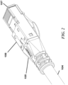
- An initial embodiment of a modular connector plug as represented in Figs. 1 and 2 is configured to form a connector interface with a corresponding female connector jack (not shown) including a plurality of female jack contacts in a high speed data transmission network.
- a housing is formed of an insulating (e.g., plastic) plug body 107 in operative attachment with a conductive (e.g., metal) shield 106 and an insulating (e.g., plastic) strain relieving body 105.
- the plug is applied to shielded twisted pair cable 104.
- Within the plug body is a plug sub-assembly 108. When the plug is to be terminated in the field, it may be supplied in an unassembled configuration (see, e.g., as represented in Figure 3 ).
- Figure 4 shows the strain relief 105 and the outer shield 106 in greater detail. Integral to the strain relief 105 are a cable flexing portion 105a, a tab anti-snag portion 105b and a plurality of latch features 105c that engage with shield apertures (e.g., cut-outs) 106e thus locating and retaining the outer shield 106.
- shield apertures e.g., cut-outs
- the outer shield 106 may also be constructed with additional integral features.
- shield retention tabs 106a are formed over once the shield 106 and strain relief 105 are assembled to the plug sub assembly 108 and plug body 107. These retention tabs 106a assist in holding the plug together.
- the electrical ground path of the plug connector is maintained by the cable ground springs 106b and the jack ground tabs 106c.
- the cable ground springs 106b are formed inward from the main shield 106 and make contact with the foil shields 170a of the twisted pairs 170.
- the ground path continues through the shield 106 and then continues through the plug ground tabs 106c.
- These plug ground tabs 106c are disposed on either side of the plug body 107 and make contact with ground springs that are present in typical jack connectors.
- Plug housing latches 106f engage with cut-outs 107d in the front housing 107.
- FIGS 5 and 6 show an exemplary embodiment of the plug sub-assembly 108. These two figures are shown in the assembled ( Figure 5 ) and unassembled or exploded ( Figure 6 ) configurations.
- the crimp ferrule 160 is shown in an uncrimped state 160a and in a crimped state 160b. Exemplary assembly and functionality of this plug subassembly 108 may be further detailed hereinafter.
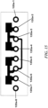
- Figure 7 shows the contacts 130 inserted into a contact retainer 140 and placed onto a primary printed circuit board (PCB) 110.
- the contacts are held in place by the interference between slots 140b in the contact retainer 140 and an integral barb portion 130a of the contacts 130.
- PCB 110 is a multilayer circuit board that provides electrical signal and ground connection paths between the shielded twisted pair cable 104 and the plug signal contacts 130 and ground contacts 106c.
- the plug contacts 130 are electrically connected to PCB 110 by means of plated-through-holes 110b , and as further noted below, the cable pairs 170 are electrically connected to conductive pads 110a.
- the electrical paths between the plug contacts 130 and the cable pairs 170 are controlled by matched impedance conductive traces. Also controlled are the inductance and electrical length of the electrical pathways.
- each plug contact 130 includes a first end connected to the PCB 110 via a respective through-hole 110b.
- the first ends of each respective plug contact 130 extend in transverse orientation with respect to a length of the PCB 110.
- the first end of each plug contact 130 may in an embodiment also be at least coincident with a lower plane of the PCB 110.
- Each plug contact 130 further includes a second end which extends in parallel with the other respective second ends of the other plug contacts and in transverse orientation with respect to the length of the PCB 110. In the configuration shown, when the first end of each plug contact 130 is connected to the PCB 110 at a respective contact hole 110b, the second end of each plug contact overhangs the end of the PCB.
- Each plug contact 130 further includes what may be referred to herein as a bridge portion between the respective first end and second end.
- the resulting shape of each plug contact 130 may resemble a staple as shown in Fig. 8 , having, for example, rounded engagement portions between the bridge and the respective ends.
- plug contact configurations are not necessarily so limited, however, and in alternative embodiments within the scope of the present disclosure it may be understood that the engagement portions may be squared, beveled, or the like.
- some of the contacts namely 130-3 and 130-5 (see contact detail in figure 8 ) are partially wider (see, e.g., 130d) than other contacts. All contacts are aligned linearly in the connector front facing the jack, but the odd-numbered contacts 130-1, 130-3, 130-5 and 130-7 are in general shorter the even-numbered contacts 130-2, 130-4, 130-6, 130-8.
- the contact through-holes 110b may accordingly form two rows including a row of first contact through-holes and a row of second contact through-holes, wherein the first contact through-holes are closer to the front end of the PCB 110 as facing the jack.
- a high capacitive coupling is selectively created, e.g., between contact pair 130-3 and 130-4 and also contact pair 130-5 and 130-6.
- These contact pairs are located in the contact retainer 140 which is composed of an isolative material.
- the characteristic dielectric properties of this isolative material are known and controlled, thus producing a controlled capacitance between the contact pairs. Because this capacitance is intimately located at the point of contact between the plug and jack contacts, there is little to no signal delay (and phase shift) resulting in very effective capacitive compensation.
- _additional capacitive compensation is provided by the secondary PCB 120 (see Figure 6 ).
- the capacitance values developed by the secondary PCB 120 are generated by controlling the area and separation distance between parallel plates 120b constructed within the layers of the secondary PCB. Controlling the area, distance and dielectric constant of the insulative PCB material will control the capacitance values in the compensation zones 120c.
- the compensation plates 120b may in an exemplary embodiment be created as integral portions of the top copper layer 120d and the bottom copper layer 120e. They provide compensation for both near end cross-talk (NEXT) and return loss (RL).
- the value of each of said capacitors is from 100 femto-farads to 3000 femto-farads, depending for example upon the design intent.
- PCB 120 is located at a distal end (e.g., on the tips) of the plug contacts.
- the plug contacts are preferably relatively short in length, such that the compensation capacitance provided by the secondary PCB 120 is located in the immediate vicinity of the jack! plug interface. This location of the compensation capacitance is also specifically offset from or otherwise outside of the current path between the jack/plug interface and the plug cable.
- the connection between the compensation 120c and the plug contacts 130 is made by way of plated-through-holes 120a-1 through 120a-8.
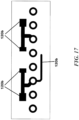
- the primary PCB 110 Within the primary PCB 110 are two or more horizontal ground planes 110g that provide electrical shielding and isolation between cable pairs 170 that are terminated to the top and bottom of the primary PCB.
- An additional vertical (i.e., orthogonal in orientation with respect to a surface plane of the primary PCB) shield 150 is attached to the primary PCB 110 and commoned to the ground plane(s) that reside in the primary PCB 110.
- This shield 150 composed of metal or other conductive substance, provides electrical shielding and isolation between cable pairs 170 that are terminated to the right and left sides of the primary PCB. This electrical shielding acts to mitigate exchange of high frequency electrical signals between cable pairs 170.
- Shield 150 is located by a plated-through-hole 110c and within an air-gap slot 110d.
- the air-gap 110d is arranged along a longitudinal axis of the primary PCB and in parallel with the adjacent conductor traces. This is done to avoid any inductive resonance coupling between the paths of the signal pairs.
- the conductive paths between the cable solder pads 110a and the contact plated through holes 110b-1 through 110b-8 are shown as signal traces 110t. These are portions of both the top copper layer 110h and bottom copper layer 110k. For each signal pair, the traces 110t are located over a ground plane 110g in parallel orientation to generate controlled impedance zones 110i. The control is maintained by prescribing the width of the traces 110t, the spacing between the traces 110t and ground planes 110g.
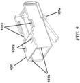
- FIG. 9 An exemplary embodiment of the front plug housing 107 is shown in Figure 9 .
- the plug latch 107a engages with the latching feature in standard jacks to provide easily accessible and positive connector engagement and retention.
- At the rear of the plug housing 107 are the entrances of the plug subassembly guide slots 107b.
- the terminated plug subassembly 108 is inserted into these slots.
- the slots locate and retain the subassembly 108 to ensure proper electrical and mechanical performance.
- the contact retainer latches 140a engage with the notches 107c in the sides of the front housing 107. This ensures retention and location of the subassembly 108.
- Latching holes 107d are also provided to retain the main shield 106 and the front housing 107 during the manufacturing process and after final assembly.
- Figure 10 shows the plug subassembly 108 terminated to the shielded twisted pair cable 104.
- the strain relief and main shield are threaded over the end of the cable.
- the crimp ferrule 160a is also threaded over the end of the cable. These are then pushed up the cable and out of the way during cable preparation.
- the cable jacket 104a is initially removed from the end of the cable 104, and the four twisted pairs 170 are separated.
- the shielding foil 170a is cut back from the ends of the pairs 170, and a short section of the wire insulation 170b is cut off, exposing the signal conductors 170c.
- the conductors 170c are arranged in the proper wiring pattern.
- the conductors 170c are terminated to the conductive pads 110a on PCB 110.
- the conductors are attached by means of welding, soldering or similar process.
- the crimp ferrule 160a is pushed toward the plug subassembly 108.
- the crimp ferrule 160a is aligned with the notch 150a in the vertical shield 150, and then crimped with an appropriate termination tool. Crimping of the crimp ferrule, now 160b, acts to common the shielding of the twisted pairs 170a and the vertical shield of the plug subassembly 108 and thus to the ground plane(s) of the primary PCB 110.
- the terminated plug assembly 108 is then inserted into the slots 107b in the front housing 107.
- the subassembly is pushed forward until the latches 140a fully engage with the front housing notches 107c.
- the strain relief 105 and main shield 106 are then pushed up over the front housing 107 and latched in place.
- the plug is now fully assembled and ready for testing and use.
Landscapes
- Engineering & Computer Science (AREA)
- Microelectronics & Electronic Packaging (AREA)
- Details Of Connecting Devices For Male And Female Coupling (AREA)
Claims (15)
- Appareil de fiche de connecteur modulaire pour former une interface de connecteur avec une prise jack de connecteur dans un réseau de transmission de données à grande vitesse, comprenant un boîtier et un sous-ensemble de contacts configuré pour être positionné à l'intérieur dudit boîtier et comprenant en outre une première carte de circuit imprimé (PCB) présentant une première extrémité et une seconde extrémité, la seconde extrémité comprenant des plots de montage conducteurs (110a) pour chacune d'une pluralité de paires de câbles (170), dans lequel :le boîtier comprend une partie avant isolante (107) et une partie de blindage conductrice (106) pouvant être fixées pour définir l'intérieur, etle sous-ensemble de contacts (108) comprend une pluralité de contacts enfichables allongés (130) comprenant chacun une première extrémité montée sur la première extrémité de la première PCB (110), une seconde extrémité distale par rapport à la première extrémité, et une partie de pont entre celles-ci, les parties de pont de la pluralité de contacts enfichables définissant collectivement une interface pour des contacts correspondants d'une prise jack de connecteur, l'appareil étant caractérisé en ce que :les secondes extrémités respectives de la pluralité de contacts enfichables sont montées sur une seconde PCB (120),dans lequel la seconde PCB comprend des plaques parallèles (120b) construites dans des couches de la seconde PCB et dont la surface et la distance de séparation sont configurées pour conférer à l'appareil des propriétés de compensation de capacité supplémentaires, et dans lequel l'emplacement de la compensation de capacité est décalé par rapport à un trajet de signal défini entre l'interface connecteur-prise jack et les paires de câbles.
- Appareil selon la revendication 1, dans lequel la première PCB comprend en outre :des trous traversants (110b) pour recevoir les premières extrémités respectives des contacts enfichables ; etun entrefer (110d) fendu à partir de la seconde extrémité et s'étendant parallèlement à des traçages électriques (110i) entre les trous traversants et les plots de montage (110a).
- Appareil selon la revendication 2, comprenant un blindage conducteur sensiblement plan (150) situé à l'intérieur de l'entrefer fendu et commun à un ou plusieurs plans de masse (110g) à l'intérieur de la première PCB, dans une orientation orthogonale par rapport à un plan de surface de la première PCB.
- Appareil selon la revendication 3, dans lequel des première et deuxième paires de plots de montage conducteurs sont prévues sur une première surface de la première PCB, et positionnées respectivement sur des premier et second côtés opposés du blindage conducteur plan, et
des troisième et quatrième paires de plots de montage conducteurs sont prévues sur une seconde surface opposée de la première PCB, et positionnées respectivement sur les premier et second côtés opposés du blindage conducteur plan. - Appareil selon l'une quelconque des revendications 1 à 4, dans lequel le sous-ensemble de contacts comprend un dispositif de retenue de contacts (140) configuré pour recevoir la pluralité de contacts et composé d'un matériau isolant présentant des propriétés diélectriques caractéristiques fournissant une compensation de capacité supplémentaire entre des paires de contacts adjacentes et un décalage par rapport au trajet de signal.
- Appareil selon la revendication 5, dans lequel le dispositif de retenue de contacts comprend des première et seconde parties latérales opposées avec des saillies (140a) s'étendant à partir de celles-ci, et
dans lequel la partie avant du boîtier comprend des première et seconde fentes intérieures correspondantes (107b) configurées pour recevoir de manière coulissante les première et seconde parties latérales opposées via les saillies. - Appareil selon la revendication 6, dans lequel les première et seconde fentes intérieures comprennent des encoches (107c) le long de leurs longueurs respectives, et les saillies sont configurées pour se comprimer lors de l'insertion dans la partie avant du boîtier et s'étendre ensuite vers l'extérieur pour venir en prise avec les encoches.
- Appareil selon la revendication 7, dans lequel la partie avant du boîtier comprend un côté supérieur présentant une ou plusieurs ouvertures (107d), et la partie de blindage conductrice du boîtier comprend un ou plusieurs verrous respectifs (106f) configurés pour venir en prise avec les une ou plusieurs ouvertures lorsque la partie avant et la partie de blindage conductrice viennent en prise de manière coulissante.
- Appareil selon la revendication 8, dans lequel la partie de blindage conductrice comprend des pattes de mise à la terre de prise jack (106c) s'étendant le long de première et seconde parois latérales extérieures opposées de la partie avant du boîtier lorsque la partie avant et la partie de blindage conductrice viennent en prise de manière coulissante.
- Appareil selon la revendication 9, dans lequel les première et seconde pattes de mise à la terre de prise jack comprennent en outre respectivement des pattes de retenue de blindage (106a) configurées pour se replier sur les encoches des première et seconde fentes intérieures lorsque la partie avant et la partie de blindage conductrice viennent en prise de manière coulissante, en outre pour venir en prise avec les saillies du dispositif de retenue de contacts lorsqu'étendues vers l'extérieur et retenues à l'intérieur.
- Appareil selon l'une quelconque des revendications 1 à 10, dans lequel la partie de pont pour chaque contact enfichable présente une largeur maximale s'étendant dans une direction perpendiculaire à une longueur de PCB, au moins un contact enfichable présentant une largeur maximale supérieure à la largeur maximale d'un autre contact enfichable,
dans lequel chaque contact enfichable définit une électrode d'une autre capacité de compensation formée entre des paires adjacentes de contacts enfichables, chaque autre capacité de compensation étant définie au moins partiellement par une distance entre la paire adjacente respective de contacts enfichables au niveau de l'interface de contact. - Appareil selon la revendication 11, dans lequel la partie de pont respective pour chaque contact enfichable présente une longueur s'étendant entre la première extrémité et la seconde extrémité, au moins un contact enfichable présentant une longueur de partie de pont plus courte que la longueur de partie de pont d'un autre contact enfichable.
- Appareil selon la revendication 12, dans lequel les premières extrémités respectives pour une première pluralité de contacts enfichables et une seconde pluralité de contacts enfichables sont situées dans des premier et second plans espacés parallèles.
- Appareil selon l'une quelconque des revendications 1 à 13, dans lequel une valeur de la compensation de capacité est définie par une constante diélectrique associée aux plaques parallèles (120b).
- Appareil selon l'une quelconque des revendications 1 à 14, dans lequel le sous-ensemble de contacts est configuré pour faire face à 1 000 VDC entre deux contacts adjacents quelconques, et 1 500 VDC entre deux contacts non adjacents quelconques et/ou entre un contact quelconque et le blindage conducteur, sans court-circuit ou choc électrique.
Applications Claiming Priority (3)
| Application Number | Priority Date | Filing Date | Title |
|---|---|---|---|
| US201862624479P | 2018-01-31 | 2018-01-31 | |
| US16/262,696 US10530106B2 (en) | 2018-01-31 | 2019-01-30 | Modular plug connector with multilayer PCB for very high speed applications |
| PCT/US2019/016042 WO2019152644A1 (fr) | 2018-01-31 | 2019-01-31 | Connecteur à fiche mâle modulaire ayant une carte de circuit imprimé multicouche pour des applications à très haute vitesse |
Publications (2)
| Publication Number | Publication Date |
|---|---|
| EP3747088A1 EP3747088A1 (fr) | 2020-12-09 |
| EP3747088B1 true EP3747088B1 (fr) | 2023-02-22 |
Family
ID=67391638
Family Applications (1)
| Application Number | Title | Priority Date | Filing Date |
|---|---|---|---|
| EP19705667.4A Active EP3747088B1 (fr) | 2018-01-31 | 2019-01-31 | Connecteur à fiche mâle modulaire ayant une carte de circuit imprimé multicouche pour des applications à très haute vitesse |
Country Status (5)
| Country | Link |
|---|---|
| US (1) | US10530106B2 (fr) |
| EP (1) | EP3747088B1 (fr) |
| JP (1) | JP2021507490A (fr) |
| CN (1) | CN111699595A (fr) |
| WO (1) | WO2019152644A1 (fr) |
Families Citing this family (4)
| Publication number | Priority date | Publication date | Assignee | Title |
|---|---|---|---|---|
| US11476616B2 (en) | 2020-02-05 | 2022-10-18 | Panduit Corp. | Modular communications plug |
| DE102020105994A1 (de) * | 2020-03-05 | 2021-09-09 | Te Connectivity Germany Gmbh | Robustes, hochfrequenz-geeignetes elektrisches Terminal |
| KR102818147B1 (ko) * | 2021-03-04 | 2025-06-11 | 엘에스전선 주식회사 | 모듈러잭 |
| DE102022127543A1 (de) * | 2022-10-19 | 2024-04-25 | Weidmüller Interface GmbH & Co. KG | Steckanordnung und Ethernet-Datensteckverbinder |
Citations (1)
| Publication number | Priority date | Publication date | Assignee | Title |
|---|---|---|---|---|
| US9601886B1 (en) * | 2016-02-23 | 2017-03-21 | Panduit Corp. | Communication plugs and components thereof |
Family Cites Families (76)
| Publication number | Priority date | Publication date | Assignee | Title |
|---|---|---|---|---|
| US5639266A (en) | 1994-01-11 | 1997-06-17 | Stewart Connector Systems, Inc. | High frequency electrical connector |
| JP2003522368A (ja) | 1998-04-16 | 2003-07-22 | トーマス アンド ベッツ インターナショナル,インク. | 漏話低減電気ジャックおよびプラグコネクタ |
| US6642456B2 (en) | 1998-05-15 | 2003-11-04 | Servicios Condumex | Flexible automotive electrical conductor of high mechanical strength using a central wire of copper clad steel and the process for manufacture thereof |
| US6042427A (en) | 1998-06-30 | 2000-03-28 | Lucent Technologies Inc. | Communication plug having low complementary crosstalk delay |
| GB2343558B (en) | 1998-11-04 | 2002-10-30 | Itt Mfg Enterprises Inc | Electrical connector |
| US6447326B1 (en) * | 2000-08-09 | 2002-09-10 | Panduit Corp. | Patch cord connector |
| WO2001052364A1 (fr) * | 2000-01-14 | 2001-07-19 | Panduit Corp. | Connecteur de communication modulaire a faible diaphonie |
| EP1128491B1 (fr) | 2000-02-21 | 2004-09-15 | Reichle & De-Massari AG | Elément de connecteur électrique |
| US6896557B2 (en) | 2001-03-28 | 2005-05-24 | Ortronics, Inc. | Dual reactance low noise modular connector insert |
| US6464541B1 (en) | 2001-05-23 | 2002-10-15 | Avaya Technology Corp. | Simultaneous near-end and far-end crosstalk compensation in a communication connector |
| US6749444B2 (en) | 2002-01-16 | 2004-06-15 | Tyco Electronics Corporation | Connector with interchangeable impedance tuner |
| US6881096B2 (en) | 2002-04-15 | 2005-04-19 | Lantronix, Inc. | Compact serial-to-ethernet conversion port |
| US7153163B2 (en) | 2002-07-16 | 2006-12-26 | Tyco Electronics Corporation | Modular jack for ethernet applications |
| US6695649B1 (en) | 2002-08-05 | 2004-02-24 | Panduit Corp | Vertical PCB jack with shield |
| US7182649B2 (en) | 2003-12-22 | 2007-02-27 | Panduit Corp. | Inductive and capacitive coupling balancing electrical connector |
| WO2005091444A1 (fr) | 2004-03-12 | 2005-09-29 | Panduit Corp. | Methodes et appareil pour reduire la diaphonie dans des connecteurs electriques |
| US7153168B2 (en) | 2004-04-06 | 2006-12-26 | Panduit Corp. | Electrical connector with improved crosstalk compensation |
| US7229309B2 (en) * | 2004-06-24 | 2007-06-12 | James A. Carroll | Network connection system |
| EP1774625B1 (fr) | 2004-07-13 | 2014-06-25 | Panduit Corporation | Connecteur de communication avec une carte de circuit imprime flexible |
| US7201618B2 (en) | 2005-01-28 | 2007-04-10 | Commscope Solutions Properties, Llc | Controlled mode conversion connector for reduced alien crosstalk |
| US20070040645A1 (en) | 2005-08-19 | 2007-02-22 | Sedio Stephen M | Transformer And Method Of Winding Same |
| US10049803B2 (en) | 2005-09-22 | 2018-08-14 | Radial Electronics, Inc. | Arrayed embedded magnetic components and methods |
| US7628656B2 (en) | 2006-03-10 | 2009-12-08 | Tyco Electronics Corporation | Receptacle with crosstalk optimizing contact array |
| JP2007250818A (ja) | 2006-03-16 | 2007-09-27 | Fujitsu Ltd | 回路基板 |
| US7686650B2 (en) | 2006-05-17 | 2010-03-30 | Bel Fuse Ltd. | High speed modular jack with flexible compensation circuit |
| WO2008076813A2 (fr) | 2006-12-13 | 2008-06-26 | Panduit Corp. | Prise de communication comportant des contacts d'interface de fiche en couches |
| US20080200060A1 (en) | 2007-02-16 | 2008-08-21 | Buckmeier Brian J | Electrical Isolation Device Capable Of Limiting Magnetic Saturation Even Upon Receipt Of High Power DC Bias And Method For Making The Same |
| US7429195B2 (en) | 2007-02-16 | 2008-09-30 | Bel Fuse (Macao Commercial Offshore) Ltd. | Connector including isolation magnetic devices capable of handling high speed communications |
| US7481678B2 (en) | 2007-06-14 | 2009-01-27 | Ortronics, Inc. | Modular insert and jack including bi-sectional lead frames |
| FR2919434B1 (fr) | 2007-07-25 | 2009-10-23 | Legrand France | Connecteur pour reseaux informatiques. |
| US7857635B2 (en) | 2007-09-12 | 2010-12-28 | Commscope, Inc. Of North Carolina | Board edge termination back-end connection assemblies and communications connectors including such assemblies |
| US7736195B1 (en) | 2009-03-10 | 2010-06-15 | Leviton Manufacturing Co., Inc. | Circuits, systems and methods for implementing high speed data communications connectors that provide for reduced modal alien crosstalk in communications systems |
| US20090265918A1 (en) | 2008-04-23 | 2009-10-29 | Dounaevsky Oleg | System and method for automated production of rf chokes |
| US7658651B2 (en) | 2008-04-25 | 2010-02-09 | Tyco Electronics Corporation | Electrical connectors and circuit boards having non-ohmic plates |
| DE102008027512B4 (de) * | 2008-06-10 | 2010-07-01 | Tyco Electronics Amp Gmbh | Elektrischer Stecker |
| US7914345B2 (en) | 2008-08-13 | 2011-03-29 | Tyco Electronics Corporation | Electrical connector with improved compensation |
| TW201010211A (en) | 2008-08-19 | 2010-03-01 | John Peng | Network jack and method for processing the same |
| AU2009282836A1 (en) | 2008-08-20 | 2010-02-25 | Panduit Corp. | High-speed connector with multi-stage compensation |
| US7924130B2 (en) | 2008-08-20 | 2011-04-12 | Bel Fuse (Macao Commercial Offshore) Limited | Isolation magnetic devices capable of handling high speed communications |
| US8167661B2 (en) | 2008-12-02 | 2012-05-01 | Panduit Corp. | Method and system for improving crosstalk attenuation within a plug/jack connection and between nearby plug/jack combinations |
| US7794286B2 (en) | 2008-12-12 | 2010-09-14 | Hubbell Incorporated | Electrical connector with separate contact mounting and compensation boards |
| US8197286B2 (en) * | 2009-06-11 | 2012-06-12 | Commscope, Inc. Of North Carolina | Communications plugs having capacitors that inject offending crosstalk after a plug-jack mating point and related connectors and methods |
| GB0914025D0 (en) | 2009-08-11 | 2009-09-16 | 3M Innovative Properties Co | Telecommunications connector |
| US8435082B2 (en) | 2010-08-03 | 2013-05-07 | Tyco Electronics Corporation | Electrical connectors and printed circuits having broadside-coupling regions |
| US7967644B2 (en) | 2009-08-25 | 2011-06-28 | Tyco Electronics Corporation | Electrical connector with separable contacts |
| US8395329B2 (en) | 2009-09-09 | 2013-03-12 | Bel Fuse (Macao Commercial Offshore) | LED ballast power supply having digital controller |
| AU2010315929A1 (en) | 2009-11-03 | 2012-05-24 | Bel Fuse (Macao Commercial Offshore) Limited | Modular connector plug for high speed applications |
| TWI452582B (zh) | 2010-02-23 | 2014-09-11 | Pulse Electronics Corp | 編織導線、感應裝置及製造其之方法 |
| US20120076459A1 (en) | 2010-09-28 | 2012-03-29 | Bel Fuse (Macao Commercial Offshore) Limited | Fiber Optic Cable Assembly And Methods |
| US8690598B2 (en) | 2010-10-21 | 2014-04-08 | Panduit Corp. | Communication plug with improved crosstalk |
| US8480438B2 (en) | 2010-10-22 | 2013-07-09 | Adc Telecommunications, Inc. | Contact set arrangement for right angle jack |
| US8952707B2 (en) | 2011-01-21 | 2015-02-10 | Commscope, Inc. Of North Carolina | Plug insertion detection circuits and related methods and communications connectors |
| EP2487761B1 (fr) | 2011-02-10 | 2013-07-31 | 3M Innovative Properties Company | Connecteur de télécommunication |
| SG185162A1 (en) | 2011-04-28 | 2012-11-29 | 3M Innovative Properties Co | An electrical connector |
| JP5854761B2 (ja) * | 2011-10-28 | 2016-02-09 | スリーエム イノベイティブ プロパティズ カンパニー | 電気コネクタ |
| US8920199B2 (en) * | 2012-02-13 | 2014-12-30 | Commscope, Inc. Of North Carolina | Patch cord having a plug with differential transmission lines |
| US9509107B2 (en) * | 2012-02-13 | 2016-11-29 | Commscope, Inc. Of North Carolina | Communication patch cord having a plug with contact blades connected to conductors of a cable |
| CN104247165B (zh) | 2012-02-13 | 2016-11-09 | 美国北卡罗来纳康普公司 | 具有低剖面表面安装的印刷电路板插头叶片的小形状因数模块化插头 |
| US9112320B2 (en) * | 2012-02-23 | 2015-08-18 | Commscope, Inc. Of North Carolina | Communications connectors having electrically parallel sets of contacts |
| CA2782486A1 (fr) | 2012-06-28 | 2013-12-28 | Belden Cdt (Canada) Inc. | Ensemble interconnecteur haute vitesse apparie |
| US8961239B2 (en) | 2012-09-07 | 2015-02-24 | Commscope, Inc. Of North Carolina | Communication jack having a plurality of contacts mounted on a flexible printed circuit board |
| EP2765656B1 (fr) | 2013-01-23 | 2018-11-14 | CommScope, Inc. of North Carolina | Cordon de connexion |
| US8915756B2 (en) | 2013-01-23 | 2014-12-23 | Commscope, Inc. Of North Carolina | Communication connector having a printed circuit board with thin conductive layers |
| US8858268B2 (en) | 2013-03-14 | 2014-10-14 | Commscope, Inc. Of North Carolina | Communications plugs and patch cords with mode conversion control circuitry |
| US8894447B2 (en) | 2013-03-14 | 2014-11-25 | Commscope, Inc. Of North Carolina | Communication plug having a plurality of coupled conductive paths |
| US9124101B2 (en) | 2013-04-02 | 2015-09-01 | Bel Fuse (Macao Commercial Offshore) Limited | Power supply having selectable operation based on communications with load |
| CH708283A1 (de) | 2013-07-11 | 2015-01-15 | Christian Rohrer | Verwendung eines Kabels für die Übertragung von Tonsignalen. |
| FR3016740B1 (fr) * | 2014-01-17 | 2016-02-12 | Legrand France | Prise rj45 male pour cordon de raccordement electrique rj45 |
| WO2016190888A1 (fr) | 2014-06-05 | 2016-12-01 | Bel Fuse (Macao Commercial Offshore) Ltd. | Connecteur d'interface de réseau à compensation de proximité |
| US9588564B2 (en) | 2014-08-20 | 2017-03-07 | Bel Fuse (Macao Commercial Offshore) Ltd. | Power over ethernet for 10GBase-T ethernet |
| CN106019491B (zh) * | 2015-03-25 | 2019-11-01 | 富士康(昆山)电脑接插件有限公司 | 混合插座连接器及混合插头连接器 |
| US10050383B2 (en) | 2015-05-19 | 2018-08-14 | Panduit Corp. | Communication connectors |
| WO2017015459A1 (fr) | 2015-07-21 | 2017-01-26 | Bel Fuse (Macao Commercial Offshore) Limited | Fiche de connecteur modulaire pour réseaux de transmission de données à grande vitesse |
| JP6080922B2 (ja) * | 2015-08-26 | 2017-02-15 | スリーエム イノベイティブ プロパティズ カンパニー | 電気コネクタ |
| US10135207B2 (en) * | 2016-01-31 | 2018-11-20 | Leviton Manufacturing Co., Inc. | High-speed data communications connector |
| US20170317450A1 (en) * | 2016-04-29 | 2017-11-02 | Panduit Corp. | RJ Communication Connectors |
-
2019
- 2019-01-30 US US16/262,696 patent/US10530106B2/en active Active
- 2019-01-31 EP EP19705667.4A patent/EP3747088B1/fr active Active
- 2019-01-31 CN CN201980011352.8A patent/CN111699595A/zh active Pending
- 2019-01-31 WO PCT/US2019/016042 patent/WO2019152644A1/fr not_active Ceased
- 2019-01-31 JP JP2020541699A patent/JP2021507490A/ja not_active Ceased
Patent Citations (1)
| Publication number | Priority date | Publication date | Assignee | Title |
|---|---|---|---|---|
| US9601886B1 (en) * | 2016-02-23 | 2017-03-21 | Panduit Corp. | Communication plugs and components thereof |
Also Published As
| Publication number | Publication date |
|---|---|
| CN111699595A (zh) | 2020-09-22 |
| US10530106B2 (en) | 2020-01-07 |
| JP2021507490A (ja) | 2021-02-22 |
| US20190237920A1 (en) | 2019-08-01 |
| EP3747088A1 (fr) | 2020-12-09 |
| WO2019152644A8 (fr) | 2019-09-06 |
| WO2019152644A1 (fr) | 2019-08-08 |
Similar Documents
| Publication | Publication Date | Title |
|---|---|---|
| CN102668267B (zh) | 具有改进的串扰补偿的通信连接器 | |
| US11245210B2 (en) | High speed connector system | |
| JP3534478B2 (ja) | 電気コネクタ | |
| US7824231B2 (en) | Internal crosstalk compensation circuit formed on a flexible printed circuit board positioned within a communications outlet, and methods and system relating to same | |
| EP2815466B1 (fr) | Fiches rj-45 à petit facteur de forme, avec lames extraplates de fiche à carte de circuit imprimé montées en surface | |
| US9819124B2 (en) | Low crosstalk printed circuit board based communications plugs and patch cords including such plugs | |
| US8992248B2 (en) | Modular jack with enhanced port isolation | |
| EP2089889B1 (fr) | Connecteur modulaire avec une aptitude reduite a la variation des terminaisons | |
| CA2405101C (fr) | Element de connexion pour des communications de donnees a grande vitesse | |
| EP1188204B1 (fr) | Fiche electrique modulaire, ensembles fiche et cable comprenant cette fiche, et barre de charge et broche de borne pour cette fiche | |
| US7901238B1 (en) | Terminal block and board assembly for an electrical connector | |
| US9490586B1 (en) | Electrical connector having a ground shield | |
| EP3747088B1 (fr) | Connecteur à fiche mâle modulaire ayant une carte de circuit imprimé multicouche pour des applications à très haute vitesse | |
| EP2765656B1 (fr) | Cordon de connexion | |
| EP3175515B1 (fr) | Connecteurs de communication comprenant des segments de ligne de transmission à basse impédance qui améliorent l'affaiblissement de réflexion | |
| US20180248318A1 (en) | Modular jack connector | |
| WO2014186033A1 (fr) | Connecteurs de communication ayant des cartes à circuits imprimés flexibles avec compensation de diaphonie en mode commun | |
| US20180097297A1 (en) | Printed circuit board based communications plugs that are suitable for field termination and patch cords including such plugs | |
| US10439329B2 (en) | Modular connector plug for high speed data transmission networks | |
| US9819131B2 (en) | RJ-45 communication plug with plug blades received in apertures in a front edge of a printed circuit board | |
| US7967614B1 (en) | Plug connector and connector assembly having a pluggable board substrate | |
| US20140162477A1 (en) | Communications Jacks Having Low-Coupling Contacts | |
| US10637196B2 (en) | Modular jack contact assembly having controlled capacitive coupling positioned within a jack housing | |
| GB2510675A (en) | Communications jacks with contacts mounted on springs |
Legal Events
| Date | Code | Title | Description |
|---|---|---|---|
| STAA | Information on the status of an ep patent application or granted ep patent |
Free format text: STATUS: UNKNOWN |
|
| STAA | Information on the status of an ep patent application or granted ep patent |
Free format text: STATUS: THE INTERNATIONAL PUBLICATION HAS BEEN MADE |
|
| PUAI | Public reference made under article 153(3) epc to a published international application that has entered the european phase |
Free format text: ORIGINAL CODE: 0009012 |
|
| STAA | Information on the status of an ep patent application or granted ep patent |
Free format text: STATUS: REQUEST FOR EXAMINATION WAS MADE |
|
| 17P | Request for examination filed |
Effective date: 20200826 |
|
| AK | Designated contracting states |
Kind code of ref document: A1 Designated state(s): AL AT BE BG CH CY CZ DE DK EE ES FI FR GB GR HR HU IE IS IT LI LT LU LV MC MK MT NL NO PL PT RO RS SE SI SK SM TR |
|
| AX | Request for extension of the european patent |
Extension state: BA ME |
|
| DAV | Request for validation of the european patent (deleted) | ||
| DAX | Request for extension of the european patent (deleted) | ||
| STAA | Information on the status of an ep patent application or granted ep patent |
Free format text: STATUS: EXAMINATION IS IN PROGRESS |
|
| 17Q | First examination report despatched |
Effective date: 20210714 |
|
| GRAP | Despatch of communication of intention to grant a patent |
Free format text: ORIGINAL CODE: EPIDOSNIGR1 |
|
| STAA | Information on the status of an ep patent application or granted ep patent |
Free format text: STATUS: GRANT OF PATENT IS INTENDED |
|
| INTG | Intention to grant announced |
Effective date: 20220914 |
|
| GRAS | Grant fee paid |
Free format text: ORIGINAL CODE: EPIDOSNIGR3 |
|
| GRAA | (expected) grant |
Free format text: ORIGINAL CODE: 0009210 |
|
| STAA | Information on the status of an ep patent application or granted ep patent |
Free format text: STATUS: THE PATENT HAS BEEN GRANTED |
|
| AK | Designated contracting states |
Kind code of ref document: B1 Designated state(s): AL AT BE BG CH CY CZ DE DK EE ES FI FR GB GR HR HU IE IS IT LI LT LU LV MC MK MT NL NO PL PT RO RS SE SI SK SM TR |
|
| REG | Reference to a national code |
Ref country code: GB Ref legal event code: FG4D |
|
| REG | Reference to a national code |
Ref country code: CH Ref legal event code: EP |
|
| REG | Reference to a national code |
Ref country code: DE Ref legal event code: R096 Ref document number: 602019025510 Country of ref document: DE |
|
| REG | Reference to a national code |
Ref country code: AT Ref legal event code: REF Ref document number: 1550115 Country of ref document: AT Kind code of ref document: T Effective date: 20230315 Ref country code: IE Ref legal event code: FG4D |
|
| REG | Reference to a national code |
Ref country code: LT Ref legal event code: MG9D |
|
| REG | Reference to a national code |
Ref country code: NL Ref legal event code: MP Effective date: 20230222 |
|
| REG | Reference to a national code |
Ref country code: AT Ref legal event code: MK05 Ref document number: 1550115 Country of ref document: AT Kind code of ref document: T Effective date: 20230222 |
|
| PG25 | Lapsed in a contracting state [announced via postgrant information from national office to epo] |
Ref country code: RS Free format text: LAPSE BECAUSE OF FAILURE TO SUBMIT A TRANSLATION OF THE DESCRIPTION OR TO PAY THE FEE WITHIN THE PRESCRIBED TIME-LIMIT Effective date: 20230222 Ref country code: PT Free format text: LAPSE BECAUSE OF FAILURE TO SUBMIT A TRANSLATION OF THE DESCRIPTION OR TO PAY THE FEE WITHIN THE PRESCRIBED TIME-LIMIT Effective date: 20230622 Ref country code: NO Free format text: LAPSE BECAUSE OF FAILURE TO SUBMIT A TRANSLATION OF THE DESCRIPTION OR TO PAY THE FEE WITHIN THE PRESCRIBED TIME-LIMIT Effective date: 20230522 Ref country code: NL Free format text: LAPSE BECAUSE OF FAILURE TO SUBMIT A TRANSLATION OF THE DESCRIPTION OR TO PAY THE FEE WITHIN THE PRESCRIBED TIME-LIMIT Effective date: 20230222 Ref country code: LV Free format text: LAPSE BECAUSE OF FAILURE TO SUBMIT A TRANSLATION OF THE DESCRIPTION OR TO PAY THE FEE WITHIN THE PRESCRIBED TIME-LIMIT Effective date: 20230222 Ref country code: LT Free format text: LAPSE BECAUSE OF FAILURE TO SUBMIT A TRANSLATION OF THE DESCRIPTION OR TO PAY THE FEE WITHIN THE PRESCRIBED TIME-LIMIT Effective date: 20230222 Ref country code: HR Free format text: LAPSE BECAUSE OF FAILURE TO SUBMIT A TRANSLATION OF THE DESCRIPTION OR TO PAY THE FEE WITHIN THE PRESCRIBED TIME-LIMIT Effective date: 20230222 Ref country code: ES Free format text: LAPSE BECAUSE OF FAILURE TO SUBMIT A TRANSLATION OF THE DESCRIPTION OR TO PAY THE FEE WITHIN THE PRESCRIBED TIME-LIMIT Effective date: 20230222 Ref country code: AT Free format text: LAPSE BECAUSE OF FAILURE TO SUBMIT A TRANSLATION OF THE DESCRIPTION OR TO PAY THE FEE WITHIN THE PRESCRIBED TIME-LIMIT Effective date: 20230222 |
|
| PG25 | Lapsed in a contracting state [announced via postgrant information from national office to epo] |
Ref country code: SE Free format text: LAPSE BECAUSE OF FAILURE TO SUBMIT A TRANSLATION OF THE DESCRIPTION OR TO PAY THE FEE WITHIN THE PRESCRIBED TIME-LIMIT Effective date: 20230222 Ref country code: PL Free format text: LAPSE BECAUSE OF FAILURE TO SUBMIT A TRANSLATION OF THE DESCRIPTION OR TO PAY THE FEE WITHIN THE PRESCRIBED TIME-LIMIT Effective date: 20230222 Ref country code: IS Free format text: LAPSE BECAUSE OF FAILURE TO SUBMIT A TRANSLATION OF THE DESCRIPTION OR TO PAY THE FEE WITHIN THE PRESCRIBED TIME-LIMIT Effective date: 20230622 Ref country code: GR Free format text: LAPSE BECAUSE OF FAILURE TO SUBMIT A TRANSLATION OF THE DESCRIPTION OR TO PAY THE FEE WITHIN THE PRESCRIBED TIME-LIMIT Effective date: 20230523 Ref country code: FI Free format text: LAPSE BECAUSE OF FAILURE TO SUBMIT A TRANSLATION OF THE DESCRIPTION OR TO PAY THE FEE WITHIN THE PRESCRIBED TIME-LIMIT Effective date: 20230222 |
|
| PG25 | Lapsed in a contracting state [announced via postgrant information from national office to epo] |
Ref country code: SM Free format text: LAPSE BECAUSE OF FAILURE TO SUBMIT A TRANSLATION OF THE DESCRIPTION OR TO PAY THE FEE WITHIN THE PRESCRIBED TIME-LIMIT Effective date: 20230222 Ref country code: RO Free format text: LAPSE BECAUSE OF FAILURE TO SUBMIT A TRANSLATION OF THE DESCRIPTION OR TO PAY THE FEE WITHIN THE PRESCRIBED TIME-LIMIT Effective date: 20230222 Ref country code: EE Free format text: LAPSE BECAUSE OF FAILURE TO SUBMIT A TRANSLATION OF THE DESCRIPTION OR TO PAY THE FEE WITHIN THE PRESCRIBED TIME-LIMIT Effective date: 20230222 Ref country code: DK Free format text: LAPSE BECAUSE OF FAILURE TO SUBMIT A TRANSLATION OF THE DESCRIPTION OR TO PAY THE FEE WITHIN THE PRESCRIBED TIME-LIMIT Effective date: 20230222 Ref country code: CZ Free format text: LAPSE BECAUSE OF FAILURE TO SUBMIT A TRANSLATION OF THE DESCRIPTION OR TO PAY THE FEE WITHIN THE PRESCRIBED TIME-LIMIT Effective date: 20230222 |
|
| REG | Reference to a national code |
Ref country code: DE Ref legal event code: R097 Ref document number: 602019025510 Country of ref document: DE |
|
| PG25 | Lapsed in a contracting state [announced via postgrant information from national office to epo] |
Ref country code: SK Free format text: LAPSE BECAUSE OF FAILURE TO SUBMIT A TRANSLATION OF THE DESCRIPTION OR TO PAY THE FEE WITHIN THE PRESCRIBED TIME-LIMIT Effective date: 20230222 |
|
| PLBE | No opposition filed within time limit |
Free format text: ORIGINAL CODE: 0009261 |
|
| STAA | Information on the status of an ep patent application or granted ep patent |
Free format text: STATUS: NO OPPOSITION FILED WITHIN TIME LIMIT |
|
| 26N | No opposition filed |
Effective date: 20231123 |
|
| PG25 | Lapsed in a contracting state [announced via postgrant information from national office to epo] |
Ref country code: SI Free format text: LAPSE BECAUSE OF FAILURE TO SUBMIT A TRANSLATION OF THE DESCRIPTION OR TO PAY THE FEE WITHIN THE PRESCRIBED TIME-LIMIT Effective date: 20230222 |
|
| PG25 | Lapsed in a contracting state [announced via postgrant information from national office to epo] |
Ref country code: IT Free format text: LAPSE BECAUSE OF FAILURE TO SUBMIT A TRANSLATION OF THE DESCRIPTION OR TO PAY THE FEE WITHIN THE PRESCRIBED TIME-LIMIT Effective date: 20230222 |
|
| PG25 | Lapsed in a contracting state [announced via postgrant information from national office to epo] |
Ref country code: MC Free format text: LAPSE BECAUSE OF FAILURE TO SUBMIT A TRANSLATION OF THE DESCRIPTION OR TO PAY THE FEE WITHIN THE PRESCRIBED TIME-LIMIT Effective date: 20230222 |
|
| PG25 | Lapsed in a contracting state [announced via postgrant information from national office to epo] |
Ref country code: MC Free format text: LAPSE BECAUSE OF FAILURE TO SUBMIT A TRANSLATION OF THE DESCRIPTION OR TO PAY THE FEE WITHIN THE PRESCRIBED TIME-LIMIT Effective date: 20230222 |
|
| PG25 | Lapsed in a contracting state [announced via postgrant information from national office to epo] |
Ref country code: LU Free format text: LAPSE BECAUSE OF NON-PAYMENT OF DUE FEES Effective date: 20240131 |
|
| PG25 | Lapsed in a contracting state [announced via postgrant information from national office to epo] |
Ref country code: LU Free format text: LAPSE BECAUSE OF NON-PAYMENT OF DUE FEES Effective date: 20240131 |
|
| PG25 | Lapsed in a contracting state [announced via postgrant information from national office to epo] |
Ref country code: BE Free format text: LAPSE BECAUSE OF NON-PAYMENT OF DUE FEES Effective date: 20240131 |
|
| PG25 | Lapsed in a contracting state [announced via postgrant information from national office to epo] |
Ref country code: BE Free format text: LAPSE BECAUSE OF NON-PAYMENT OF DUE FEES Effective date: 20240131 |
|
| REG | Reference to a national code |
Ref country code: BE Ref legal event code: MM Effective date: 20240131 |
|
| PG25 | Lapsed in a contracting state [announced via postgrant information from national office to epo] |
Ref country code: BG Free format text: LAPSE BECAUSE OF FAILURE TO SUBMIT A TRANSLATION OF THE DESCRIPTION OR TO PAY THE FEE WITHIN THE PRESCRIBED TIME-LIMIT Effective date: 20230222 |
|
| PG25 | Lapsed in a contracting state [announced via postgrant information from national office to epo] |
Ref country code: BG Free format text: LAPSE BECAUSE OF FAILURE TO SUBMIT A TRANSLATION OF THE DESCRIPTION OR TO PAY THE FEE WITHIN THE PRESCRIBED TIME-LIMIT Effective date: 20230222 |
|
| PG25 | Lapsed in a contracting state [announced via postgrant information from national office to epo] |
Ref country code: IE Free format text: LAPSE BECAUSE OF NON-PAYMENT OF DUE FEES Effective date: 20240131 |
|
| PG25 | Lapsed in a contracting state [announced via postgrant information from national office to epo] |
Ref country code: IE Free format text: LAPSE BECAUSE OF NON-PAYMENT OF DUE FEES Effective date: 20240131 |
|
| PGFP | Annual fee paid to national office [announced via postgrant information from national office to epo] |
Ref country code: CH Payment date: 20250201 Year of fee payment: 7 |
|
| PG25 | Lapsed in a contracting state [announced via postgrant information from national office to epo] |
Ref country code: CY Free format text: LAPSE BECAUSE OF FAILURE TO SUBMIT A TRANSLATION OF THE DESCRIPTION OR TO PAY THE FEE WITHIN THE PRESCRIBED TIME-LIMIT; INVALID AB INITIO Effective date: 20190131 |
|
| PG25 | Lapsed in a contracting state [announced via postgrant information from national office to epo] |
Ref country code: HU Free format text: LAPSE BECAUSE OF FAILURE TO SUBMIT A TRANSLATION OF THE DESCRIPTION OR TO PAY THE FEE WITHIN THE PRESCRIBED TIME-LIMIT; INVALID AB INITIO Effective date: 20190131 |
|
| PG25 | Lapsed in a contracting state [announced via postgrant information from national office to epo] |
Ref country code: TR Free format text: LAPSE BECAUSE OF FAILURE TO SUBMIT A TRANSLATION OF THE DESCRIPTION OR TO PAY THE FEE WITHIN THE PRESCRIBED TIME-LIMIT Effective date: 20230222 |
|
| REG | Reference to a national code |
Ref country code: CH Ref legal event code: U11 Free format text: ST27 STATUS EVENT CODE: U-0-0-U10-U11 (AS PROVIDED BY THE NATIONAL OFFICE) Effective date: 20260201 |
|
| PGFP | Annual fee paid to national office [announced via postgrant information from national office to epo] |
Ref country code: GB Payment date: 20260114 Year of fee payment: 8 |
|
| PGFP | Annual fee paid to national office [announced via postgrant information from national office to epo] |
Ref country code: DE Payment date: 20260115 Year of fee payment: 8 |
|
| PGFP | Annual fee paid to national office [announced via postgrant information from national office to epo] |
Ref country code: FR Payment date: 20260115 Year of fee payment: 8 |