EP3748221A1 - Led-hintergrundbeleuchtungsfolie und led-hintergrundbeleuchtung - Google Patents
Led-hintergrundbeleuchtungsfolie und led-hintergrundbeleuchtung Download PDFInfo
- Publication number
- EP3748221A1 EP3748221A1 EP19748048.6A EP19748048A EP3748221A1 EP 3748221 A1 EP3748221 A1 EP 3748221A1 EP 19748048 A EP19748048 A EP 19748048A EP 3748221 A1 EP3748221 A1 EP 3748221A1
- Authority
- EP
- European Patent Office
- Prior art keywords
- led backlight
- light guide
- refractive index
- film
- guide plate
- Prior art date
- Legal status (The legal status is an assumption and is not a legal conclusion. Google has not performed a legal analysis and makes no representation as to the accuracy of the status listed.)
- Pending
Links
- 239000010410 layer Substances 0.000 claims abstract description 154
- 239000004820 Pressure-sensitive adhesive Substances 0.000 claims abstract description 102
- 239000011800 void material Substances 0.000 claims abstract description 13
- NIXOWILDQLNWCW-UHFFFAOYSA-M Acrylate Chemical compound [O-]C(=O)C=C NIXOWILDQLNWCW-UHFFFAOYSA-M 0.000 description 54
- 239000002245 particle Substances 0.000 description 39
- 239000000463 material Substances 0.000 description 37
- 239000000178 monomer Substances 0.000 description 34
- -1 polyethylene terephthalate Polymers 0.000 description 31
- 239000007788 liquid Substances 0.000 description 30
- 150000003377 silicon compounds Chemical class 0.000 description 28
- 238000000034 method Methods 0.000 description 23
- HRPVXLWXLXDGHG-UHFFFAOYSA-N Acrylamide Chemical compound NC(=O)C=C HRPVXLWXLXDGHG-UHFFFAOYSA-N 0.000 description 17
- NIXOWILDQLNWCW-UHFFFAOYSA-N acrylic acid group Chemical group C(C=C)(=O)O NIXOWILDQLNWCW-UHFFFAOYSA-N 0.000 description 15
- 125000000217 alkyl group Chemical group 0.000 description 14
- 238000004519 manufacturing process Methods 0.000 description 13
- 239000000243 solution Substances 0.000 description 13
- 229920000058 polyacrylate Polymers 0.000 description 12
- 239000000047 product Substances 0.000 description 12
- IJGRMHOSHXDMSA-UHFFFAOYSA-N Atomic nitrogen Chemical compound N#N IJGRMHOSHXDMSA-UHFFFAOYSA-N 0.000 description 11
- 239000003054 catalyst Substances 0.000 description 11
- 239000003431 cross linking reagent Substances 0.000 description 11
- 238000010298 pulverizing process Methods 0.000 description 11
- 238000001035 drying Methods 0.000 description 10
- ZWEHNKRNPOVVGH-UHFFFAOYSA-N 2-Butanone Chemical compound CCC(C)=O ZWEHNKRNPOVVGH-UHFFFAOYSA-N 0.000 description 9
- 125000000524 functional group Chemical group 0.000 description 9
- 229920001296 polysiloxane Polymers 0.000 description 9
- 239000011347 resin Substances 0.000 description 9
- 229920005989 resin Polymers 0.000 description 9
- 125000004432 carbon atom Chemical group C* 0.000 description 8
- 238000010438 heat treatment Methods 0.000 description 8
- 239000000470 constituent Substances 0.000 description 7
- IAZDPXIOMUYVGZ-UHFFFAOYSA-N Dimethylsulphoxide Chemical compound CS(C)=O IAZDPXIOMUYVGZ-UHFFFAOYSA-N 0.000 description 6
- XEKOWRVHYACXOJ-UHFFFAOYSA-N Ethyl acetate Chemical compound CCOC(C)=O XEKOWRVHYACXOJ-UHFFFAOYSA-N 0.000 description 6
- MUBZPKHOEPUJKR-UHFFFAOYSA-N Oxalic acid Chemical compound OC(=O)C(O)=O MUBZPKHOEPUJKR-UHFFFAOYSA-N 0.000 description 6
- VYPSYNLAJGMNEJ-UHFFFAOYSA-N Silicium dioxide Chemical compound O=[Si]=O VYPSYNLAJGMNEJ-UHFFFAOYSA-N 0.000 description 6
- 239000011248 coating agent Substances 0.000 description 6
- 238000000576 coating method Methods 0.000 description 6
- 238000009826 distribution Methods 0.000 description 6
- BLRPTPMANUNPDV-UHFFFAOYSA-N Silane Chemical compound [SiH4] BLRPTPMANUNPDV-UHFFFAOYSA-N 0.000 description 5
- 229910001873 dinitrogen Inorganic materials 0.000 description 5
- 238000011156 evaluation Methods 0.000 description 5
- 229920000139 polyethylene terephthalate Polymers 0.000 description 5
- 239000005020 polyethylene terephthalate Substances 0.000 description 5
- 239000011148 porous material Substances 0.000 description 5
- 229910000077 silane Inorganic materials 0.000 description 5
- 238000002834 transmittance Methods 0.000 description 5
- OZAIFHULBGXAKX-UHFFFAOYSA-N 2-(2-cyanopropan-2-yldiazenyl)-2-methylpropanenitrile Chemical compound N#CC(C)(C)N=NC(C)(C)C#N OZAIFHULBGXAKX-UHFFFAOYSA-N 0.000 description 4
- 239000004925 Acrylic resin Substances 0.000 description 4
- 229920000178 Acrylic resin Polymers 0.000 description 4
- 125000003647 acryloyl group Chemical group O=C([*])C([H])=C([H])[H] 0.000 description 4
- 125000003277 amino group Chemical group 0.000 description 4
- 125000003178 carboxy group Chemical group [H]OC(*)=O 0.000 description 4
- 239000001913 cellulose Substances 0.000 description 4
- 229920002678 cellulose Polymers 0.000 description 4
- 230000000052 comparative effect Effects 0.000 description 4
- 230000018044 dehydration Effects 0.000 description 4
- 238000006297 dehydration reaction Methods 0.000 description 4
- 229920001971 elastomer Polymers 0.000 description 4
- 239000011521 glass Substances 0.000 description 4
- 125000002887 hydroxy group Chemical group [H]O* 0.000 description 4
- ZXEKIIBDNHEJCQ-UHFFFAOYSA-N isobutanol Chemical compound CC(C)CO ZXEKIIBDNHEJCQ-UHFFFAOYSA-N 0.000 description 4
- 239000012948 isocyanate Substances 0.000 description 4
- 150000002513 isocyanates Chemical class 0.000 description 4
- 239000004973 liquid crystal related substance Substances 0.000 description 4
- 239000002904 solvent Substances 0.000 description 4
- 239000000126 substance Substances 0.000 description 4
- 125000001302 tertiary amino group Chemical group 0.000 description 4
- SMZOUWXMTYCWNB-UHFFFAOYSA-N 2-(2-methoxy-5-methylphenyl)ethanamine Chemical compound COC1=CC=C(C)C=C1CCN SMZOUWXMTYCWNB-UHFFFAOYSA-N 0.000 description 3
- QTBSBXVTEAMEQO-UHFFFAOYSA-N Acetic acid Chemical compound CC(O)=O QTBSBXVTEAMEQO-UHFFFAOYSA-N 0.000 description 3
- 239000004593 Epoxy Substances 0.000 description 3
- LFQSCWFLJHTTHZ-UHFFFAOYSA-N Ethanol Chemical compound CCO LFQSCWFLJHTTHZ-UHFFFAOYSA-N 0.000 description 3
- KFZMGEQAYNKOFK-UHFFFAOYSA-N Isopropanol Chemical compound CC(C)O KFZMGEQAYNKOFK-UHFFFAOYSA-N 0.000 description 3
- OKKJLVBELUTLKV-UHFFFAOYSA-N Methanol Chemical compound OC OKKJLVBELUTLKV-UHFFFAOYSA-N 0.000 description 3
- KWYUFKZDYYNOTN-UHFFFAOYSA-M Potassium hydroxide Chemical compound [OH-].[K+] KWYUFKZDYYNOTN-UHFFFAOYSA-M 0.000 description 3
- HEMHJVSKTPXQMS-UHFFFAOYSA-M Sodium hydroxide Chemical compound [OH-].[Na+] HEMHJVSKTPXQMS-UHFFFAOYSA-M 0.000 description 3
- 125000003368 amide group Chemical group 0.000 description 3
- BTANRVKWQNVYAZ-UHFFFAOYSA-N butan-2-ol Chemical compound CCC(C)O BTANRVKWQNVYAZ-UHFFFAOYSA-N 0.000 description 3
- 150000001875 compounds Chemical class 0.000 description 3
- 238000006482 condensation reaction Methods 0.000 description 3
- 238000001879 gelation Methods 0.000 description 3
- 125000004435 hydrogen atom Chemical group [H]* 0.000 description 3
- 230000035800 maturation Effects 0.000 description 3
- 238000005259 measurement Methods 0.000 description 3
- 239000002121 nanofiber Substances 0.000 description 3
- 229910052757 nitrogen Inorganic materials 0.000 description 3
- 238000006116 polymerization reaction Methods 0.000 description 3
- 239000000377 silicon dioxide Substances 0.000 description 3
- HBGXFGADFJLHST-UHFFFAOYSA-N silylmethanetriol Chemical compound OC(O)(O)[SiH3] HBGXFGADFJLHST-UHFFFAOYSA-N 0.000 description 3
- 239000000758 substrate Substances 0.000 description 3
- 125000000391 vinyl group Chemical group [H]C([*])=C([H])[H] 0.000 description 3
- XLPJNCYCZORXHG-UHFFFAOYSA-N 1-morpholin-4-ylprop-2-en-1-one Chemical compound C=CC(=O)N1CCOCC1 XLPJNCYCZORXHG-UHFFFAOYSA-N 0.000 description 2
- NJRHMGPRPPEGQL-UHFFFAOYSA-N 2-hydroxybutyl prop-2-enoate Chemical compound CCC(O)COC(=O)C=C NJRHMGPRPPEGQL-UHFFFAOYSA-N 0.000 description 2
- VHUUQVKOLVNVRT-UHFFFAOYSA-N Ammonium hydroxide Chemical compound [NH4+].[OH-] VHUUQVKOLVNVRT-UHFFFAOYSA-N 0.000 description 2
- 239000004342 Benzoyl peroxide Substances 0.000 description 2
- OMPJBNCRMGITSC-UHFFFAOYSA-N Benzoylperoxide Chemical compound C=1C=CC=CC=1C(=O)OOC(=O)C1=CC=CC=C1 OMPJBNCRMGITSC-UHFFFAOYSA-N 0.000 description 2
- VZCYOOQTPOCHFL-OWOJBTEDSA-N Fumaric acid Chemical compound OC(=O)\C=C\C(O)=O VZCYOOQTPOCHFL-OWOJBTEDSA-N 0.000 description 2
- VEXZGXHMUGYJMC-UHFFFAOYSA-N Hydrochloric acid Chemical compound Cl VEXZGXHMUGYJMC-UHFFFAOYSA-N 0.000 description 2
- CERQOIWHTDAKMF-UHFFFAOYSA-N Methacrylic acid Chemical compound CC(=C)C(O)=O CERQOIWHTDAKMF-UHFFFAOYSA-N 0.000 description 2
- LRHPLDYGYMQRHN-UHFFFAOYSA-N N-Butanol Chemical compound CCCCO LRHPLDYGYMQRHN-UHFFFAOYSA-N 0.000 description 2
- AMQJEAYHLZJPGS-UHFFFAOYSA-N N-Pentanol Chemical compound CCCCCO AMQJEAYHLZJPGS-UHFFFAOYSA-N 0.000 description 2
- PPBRXRYQALVLMV-UHFFFAOYSA-N Styrene Chemical compound C=CC1=CC=CC=C1 PPBRXRYQALVLMV-UHFFFAOYSA-N 0.000 description 2
- ZJCCRDAZUWHFQH-UHFFFAOYSA-N Trimethylolpropane Chemical compound CCC(CO)(CO)CO ZJCCRDAZUWHFQH-UHFFFAOYSA-N 0.000 description 2
- 150000001252 acrylic acid derivatives Chemical class 0.000 description 2
- 239000000654 additive Substances 0.000 description 2
- 230000000996 additive effect Effects 0.000 description 2
- 230000032683 aging Effects 0.000 description 2
- 238000007754 air knife coating Methods 0.000 description 2
- XXROGKLTLUQVRX-UHFFFAOYSA-N allyl alcohol Chemical compound OCC=C XXROGKLTLUQVRX-UHFFFAOYSA-N 0.000 description 2
- 235000011114 ammonium hydroxide Nutrition 0.000 description 2
- 235000019400 benzoyl peroxide Nutrition 0.000 description 2
- 239000011230 binding agent Substances 0.000 description 2
- 230000015572 biosynthetic process Effects 0.000 description 2
- CQEYYJKEWSMYFG-UHFFFAOYSA-N butyl acrylate Chemical compound CCCCOC(=O)C=C CQEYYJKEWSMYFG-UHFFFAOYSA-N 0.000 description 2
- 150000001925 cycloalkenes Chemical class 0.000 description 2
- 238000007607 die coating method Methods 0.000 description 2
- 238000003618 dip coating Methods 0.000 description 2
- 238000002296 dynamic light scattering Methods 0.000 description 2
- 230000000694 effects Effects 0.000 description 2
- 238000005227 gel permeation chromatography Methods 0.000 description 2
- 238000007756 gravure coating Methods 0.000 description 2
- 125000002768 hydroxyalkyl group Chemical group 0.000 description 2
- 125000001972 isopentyl group Chemical group [H]C([H])([H])C([H])(C([H])([H])[H])C([H])([H])C([H])([H])* 0.000 description 2
- GNARHXWTMJZNTP-UHFFFAOYSA-N methoxy-[3-(oxiran-2-ylmethoxy)propyl]silane Chemical compound CO[SiH2]CCCOCC1CO1 GNARHXWTMJZNTP-UHFFFAOYSA-N 0.000 description 2
- 239000000203 mixture Substances 0.000 description 2
- 125000004108 n-butyl group Chemical group [H]C([H])([H])C([H])([H])C([H])([H])C([H])([H])* 0.000 description 2
- 239000003921 oil Substances 0.000 description 2
- 230000003287 optical effect Effects 0.000 description 2
- 235000006408 oxalic acid Nutrition 0.000 description 2
- 229920006267 polyester film Polymers 0.000 description 2
- 239000003505 polymerization initiator Substances 0.000 description 2
- 229920002635 polyurethane Polymers 0.000 description 2
- 239000004814 polyurethane Substances 0.000 description 2
- 230000001737 promoting effect Effects 0.000 description 2
- 238000010926 purge Methods 0.000 description 2
- 238000007763 reverse roll coating Methods 0.000 description 2
- 239000007787 solid Substances 0.000 description 2
- 238000001179 sorption measurement Methods 0.000 description 2
- 238000003756 stirring Methods 0.000 description 2
- DVKJHBMWWAPEIU-UHFFFAOYSA-N toluene 2,4-diisocyanate Chemical compound CC1=CC=C(N=C=O)C=C1N=C=O DVKJHBMWWAPEIU-UHFFFAOYSA-N 0.000 description 2
- VZCYOOQTPOCHFL-UHFFFAOYSA-N trans-butenedioic acid Natural products OC(=O)C=CC(O)=O VZCYOOQTPOCHFL-UHFFFAOYSA-N 0.000 description 2
- BPSIOYPQMFLKFR-UHFFFAOYSA-N trimethoxy-[3-(oxiran-2-ylmethoxy)propyl]silane Chemical compound CO[Si](OC)(OC)CCCOCC1CO1 BPSIOYPQMFLKFR-UHFFFAOYSA-N 0.000 description 2
- JWYVGKFDLWWQJX-UHFFFAOYSA-N 1-ethenylazepan-2-one Chemical compound C=CN1CCCCCC1=O JWYVGKFDLWWQJX-UHFFFAOYSA-N 0.000 description 1
- RESPXSHDJQUNTN-UHFFFAOYSA-N 1-piperidin-1-ylprop-2-en-1-one Chemical compound C=CC(=O)N1CCCCC1 RESPXSHDJQUNTN-UHFFFAOYSA-N 0.000 description 1
- WLPAQAXAZQUXBG-UHFFFAOYSA-N 1-pyrrolidin-1-ylprop-2-en-1-one Chemical compound C=CC(=O)N1CCCC1 WLPAQAXAZQUXBG-UHFFFAOYSA-N 0.000 description 1
- WULAHPYSGCVQHM-UHFFFAOYSA-N 2-(2-ethenoxyethoxy)ethanol Chemical compound OCCOCCOC=C WULAHPYSGCVQHM-UHFFFAOYSA-N 0.000 description 1
- HLIQLHSBZXDKLV-UHFFFAOYSA-N 2-(2-hydroxyethoxy)-1-phenoxyethanol Chemical compound OCCOCC(O)OC1=CC=CC=C1 HLIQLHSBZXDKLV-UHFFFAOYSA-N 0.000 description 1
- JAHNSTQSQJOJLO-UHFFFAOYSA-N 2-(3-fluorophenyl)-1h-imidazole Chemical compound FC1=CC=CC(C=2NC=CN=2)=C1 JAHNSTQSQJOJLO-UHFFFAOYSA-N 0.000 description 1
- IMSODMZESSGVBE-UHFFFAOYSA-N 2-Oxazoline Chemical compound C1CN=CO1 IMSODMZESSGVBE-UHFFFAOYSA-N 0.000 description 1
- VUIWJRYTWUGOOF-UHFFFAOYSA-N 2-ethenoxyethanol Chemical compound OCCOC=C VUIWJRYTWUGOOF-UHFFFAOYSA-N 0.000 description 1
- 125000000954 2-hydroxyethyl group Chemical group [H]C([*])([H])C([H])([H])O[H] 0.000 description 1
- RASDUGQQSMMINZ-UHFFFAOYSA-N 2-methyl-1-piperidin-1-ylprop-2-en-1-one Chemical compound CC(=C)C(=O)N1CCCCC1 RASDUGQQSMMINZ-UHFFFAOYSA-N 0.000 description 1
- QOXOZONBQWIKDA-UHFFFAOYSA-N 3-hydroxypropyl Chemical group [CH2]CCO QOXOZONBQWIKDA-UHFFFAOYSA-N 0.000 description 1
- HMBNQNDUEFFFNZ-UHFFFAOYSA-N 4-ethenoxybutan-1-ol Chemical compound OCCCCOC=C HMBNQNDUEFFFNZ-UHFFFAOYSA-N 0.000 description 1
- SXIFAEWFOJETOA-UHFFFAOYSA-N 4-hydroxy-butyl Chemical group [CH2]CCCO SXIFAEWFOJETOA-UHFFFAOYSA-N 0.000 description 1
- GAWIXWVDTYZWAW-UHFFFAOYSA-N C[CH]O Chemical group C[CH]O GAWIXWVDTYZWAW-UHFFFAOYSA-N 0.000 description 1
- 229920000049 Carbon (fiber) Polymers 0.000 description 1
- SJIXRGNQPBQWMK-UHFFFAOYSA-N DEAEMA Natural products CCN(CC)CCOC(=O)C(C)=C SJIXRGNQPBQWMK-UHFFFAOYSA-N 0.000 description 1
- 239000004793 Polystyrene Substances 0.000 description 1
- OFOBLEOULBTSOW-UHFFFAOYSA-N Propanedioic acid Natural products OC(=O)CC(O)=O OFOBLEOULBTSOW-UHFFFAOYSA-N 0.000 description 1
- XTXRWKRVRITETP-UHFFFAOYSA-N Vinyl acetate Chemical compound CC(=O)OC=C XTXRWKRVRITETP-UHFFFAOYSA-N 0.000 description 1
- URLYGBGJPQYXBN-UHFFFAOYSA-N [4-(hydroxymethyl)cyclohexyl]methyl prop-2-enoate Chemical compound OCC1CCC(COC(=O)C=C)CC1 URLYGBGJPQYXBN-UHFFFAOYSA-N 0.000 description 1
- 239000006096 absorbing agent Substances 0.000 description 1
- 239000003377 acid catalyst Substances 0.000 description 1
- 230000001070 adhesive effect Effects 0.000 description 1
- 239000004964 aerogel Substances 0.000 description 1
- 150000001336 alkenes Chemical class 0.000 description 1
- 125000004183 alkoxy alkyl group Chemical group 0.000 description 1
- PNEYBMLMFCGWSK-UHFFFAOYSA-N aluminium oxide Inorganic materials [O-2].[O-2].[O-2].[Al+3].[Al+3] PNEYBMLMFCGWSK-UHFFFAOYSA-N 0.000 description 1
- 125000004103 aminoalkyl group Chemical group 0.000 description 1
- 239000000908 ammonium hydroxide Substances 0.000 description 1
- 239000003963 antioxidant agent Substances 0.000 description 1
- 230000003078 antioxidant effect Effects 0.000 description 1
- 239000007864 aqueous solution Substances 0.000 description 1
- 125000003118 aryl group Chemical group 0.000 description 1
- 229920005601 base polymer Polymers 0.000 description 1
- 239000000440 bentonite Substances 0.000 description 1
- 229910000278 bentonite Inorganic materials 0.000 description 1
- SVPXDRXYRYOSEX-UHFFFAOYSA-N bentoquatam Chemical compound O.O=[Si]=O.O=[Al]O[Al]=O SVPXDRXYRYOSEX-UHFFFAOYSA-N 0.000 description 1
- 125000001797 benzyl group Chemical group [H]C1=C([H])C([H])=C(C([H])=C1[H])C([H])([H])* 0.000 description 1
- 239000004917 carbon fiber Substances 0.000 description 1
- 239000013522 chelant Substances 0.000 description 1
- 239000003795 chemical substances by application Substances 0.000 description 1
- 238000007796 conventional method Methods 0.000 description 1
- 229920001577 copolymer Polymers 0.000 description 1
- LDHQCZJRKDOVOX-NSCUHMNNSA-N crotonic acid Chemical compound C\C=C\C(O)=O LDHQCZJRKDOVOX-NSCUHMNNSA-N 0.000 description 1
- 238000010908 decantation Methods 0.000 description 1
- SWXVUIWOUIDPGS-UHFFFAOYSA-N diacetone alcohol Chemical compound CC(=O)CC(C)(C)O SWXVUIWOUIDPGS-UHFFFAOYSA-N 0.000 description 1
- 238000010894 electron beam technology Methods 0.000 description 1
- YXOGSLZKOVPUMH-UHFFFAOYSA-N ethene;phenol Chemical group C=C.OC1=CC=CC=C1 YXOGSLZKOVPUMH-UHFFFAOYSA-N 0.000 description 1
- UIWXSTHGICQLQT-UHFFFAOYSA-N ethenyl propanoate Chemical compound CCC(=O)OC=C UIWXSTHGICQLQT-UHFFFAOYSA-N 0.000 description 1
- 125000005448 ethoxyethyl group Chemical group [H]C([H])([H])C([H])([H])OC([H])([H])C([H])([H])* 0.000 description 1
- 125000001495 ethyl group Chemical group [H]C([H])([H])C([H])([H])* 0.000 description 1
- 239000010419 fine particle Substances 0.000 description 1
- 239000001530 fumaric acid Substances 0.000 description 1
- 239000007789 gas Substances 0.000 description 1
- 239000008187 granular material Substances 0.000 description 1
- 125000003187 heptyl group Chemical group [H]C([*])([H])C([H])([H])C([H])([H])C([H])([H])C([H])([H])C([H])([H])C([H])([H])[H] 0.000 description 1
- 125000004051 hexyl group Chemical group [H]C([H])([H])C([H])([H])C([H])([H])C([H])([H])C([H])([H])C([H])([H])* 0.000 description 1
- 229920001519 homopolymer Polymers 0.000 description 1
- 239000000413 hydrolysate Substances 0.000 description 1
- 230000003301 hydrolyzing effect Effects 0.000 description 1
- 239000003112 inhibitor Substances 0.000 description 1
- 239000011256 inorganic filler Substances 0.000 description 1
- 229910010272 inorganic material Inorganic materials 0.000 description 1
- 239000011147 inorganic material Substances 0.000 description 1
- 229940035429 isobutyl alcohol Drugs 0.000 description 1
- 125000000959 isobutyl group Chemical group [H]C([H])([H])C([H])(C([H])([H])[H])C([H])([H])* 0.000 description 1
- 125000001449 isopropyl group Chemical group [H]C([H])([H])C([H])(*)C([H])([H])[H] 0.000 description 1
- 239000004611 light stabiliser Substances 0.000 description 1
- 238000011068 loading method Methods 0.000 description 1
- 239000000314 lubricant Substances 0.000 description 1
- VZCYOOQTPOCHFL-UPHRSURJSA-N maleic acid Chemical compound OC(=O)\C=C/C(O)=O VZCYOOQTPOCHFL-UPHRSURJSA-N 0.000 description 1
- 239000011976 maleic acid Substances 0.000 description 1
- 229910052751 metal Inorganic materials 0.000 description 1
- 239000002184 metal Substances 0.000 description 1
- VNWKTOKETHGBQD-UHFFFAOYSA-N methane Chemical compound C VNWKTOKETHGBQD-UHFFFAOYSA-N 0.000 description 1
- LVHBHZANLOWSRM-UHFFFAOYSA-N methylenebutanedioic acid Natural products OC(=O)CC(=C)C(O)=O LVHBHZANLOWSRM-UHFFFAOYSA-N 0.000 description 1
- BFXIKLCIZHOAAZ-UHFFFAOYSA-N methyltrimethoxysilane Chemical compound CO[Si](C)(OC)OC BFXIKLCIZHOAAZ-UHFFFAOYSA-N 0.000 description 1
- JMCVCHBBHPFWBF-UHFFFAOYSA-N n,n-diethyl-2-methylprop-2-enamide Chemical compound CCN(CC)C(=O)C(C)=C JMCVCHBBHPFWBF-UHFFFAOYSA-N 0.000 description 1
- RQAKESSLMFZVMC-UHFFFAOYSA-N n-ethenylacetamide Chemical compound CC(=O)NC=C RQAKESSLMFZVMC-UHFFFAOYSA-N 0.000 description 1
- 125000000740 n-pentyl group Chemical group [H]C([H])([H])C([H])([H])C([H])([H])C([H])([H])C([H])([H])* 0.000 description 1
- 239000012802 nanoclay Substances 0.000 description 1
- 239000002105 nanoparticle Substances 0.000 description 1
- JRZJOMJEPLMPRA-UHFFFAOYSA-N olefin Natural products CCCCCCCC=C JRZJOMJEPLMPRA-UHFFFAOYSA-N 0.000 description 1
- 239000012766 organic filler Substances 0.000 description 1
- 150000002978 peroxides Chemical class 0.000 description 1
- 239000000049 pigment Substances 0.000 description 1
- 239000004014 plasticizer Substances 0.000 description 1
- 229920000515 polycarbonate Polymers 0.000 description 1
- 239000004417 polycarbonate Substances 0.000 description 1
- 229920002223 polystyrene Polymers 0.000 description 1
- 239000002243 precursor Substances 0.000 description 1
- 238000002360 preparation method Methods 0.000 description 1
- 125000002914 sec-butyl group Chemical group [H]C([H])([H])C([H])([H])C([H])(*)C([H])([H])[H] 0.000 description 1
- 125000000467 secondary amino group Chemical group [H]N([*:1])[*:2] 0.000 description 1
- 125000005372 silanol group Chemical group 0.000 description 1
- 229910052710 silicon Inorganic materials 0.000 description 1
- 239000010703 silicon Substances 0.000 description 1
- 239000002356 single layer Substances 0.000 description 1
- 238000003980 solgel method Methods 0.000 description 1
- 239000012798 spherical particle Substances 0.000 description 1
- 125000004079 stearyl group Chemical group [H]C([*])([H])C([H])([H])C([H])([H])C([H])([H])C([H])([H])C([H])([H])C([H])([H])C([H])([H])C([H])([H])C([H])([H])C([H])([H])C([H])([H])C([H])([H])C([H])([H])C([H])([H])C([H])([H])C([H])([H])C([H])([H])[H] 0.000 description 1
- 239000004094 surface-active agent Substances 0.000 description 1
- 125000000999 tert-butyl group Chemical group [H]C([H])([H])C(*)(C([H])([H])[H])C([H])([H])[H] 0.000 description 1
- 238000010998 test method Methods 0.000 description 1
- 229920005992 thermoplastic resin Polymers 0.000 description 1
- 229920001187 thermosetting polymer Polymers 0.000 description 1
- LDHQCZJRKDOVOX-UHFFFAOYSA-N trans-crotonic acid Natural products CC=CC(O)=O LDHQCZJRKDOVOX-UHFFFAOYSA-N 0.000 description 1
- JCGDCINCKDQXDX-UHFFFAOYSA-N trimethoxy(2-trimethoxysilylethyl)silane Chemical compound CO[Si](OC)(OC)CC[Si](OC)(OC)OC JCGDCINCKDQXDX-UHFFFAOYSA-N 0.000 description 1
- 229920001567 vinyl ester resin Polymers 0.000 description 1
- XLYOFNOQVPJJNP-UHFFFAOYSA-N water Substances O XLYOFNOQVPJJNP-UHFFFAOYSA-N 0.000 description 1
- 238000005303 weighing Methods 0.000 description 1
Images

Classifications
-
- F—MECHANICAL ENGINEERING; LIGHTING; HEATING; WEAPONS; BLASTING
- F21—LIGHTING
- F21K—NON-ELECTRIC LIGHT SOURCES USING LUMINESCENCE; LIGHT SOURCES USING ELECTROCHEMILUMINESCENCE; LIGHT SOURCES USING CHARGES OF COMBUSTIBLE MATERIAL; LIGHT SOURCES USING SEMICONDUCTOR DEVICES AS LIGHT-GENERATING ELEMENTS; LIGHT SOURCES NOT OTHERWISE PROVIDED FOR
- F21K9/00—Light sources using semiconductor devices as light-generating elements, e.g. using light-emitting diodes [LED] or lasers
- F21K9/60—Optical arrangements integrated in the light source, e.g. for improving the colour rendering index or the light extraction
-
- G—PHYSICS
- G02—OPTICS
- G02B—OPTICAL ELEMENTS, SYSTEMS OR APPARATUS
- G02B6/00—Light guides; Structural details of arrangements comprising light guides and other optical elements, e.g. couplings
- G02B6/0001—Light guides; Structural details of arrangements comprising light guides and other optical elements, e.g. couplings specially adapted for lighting devices or systems
- G02B6/0011—Light guides; Structural details of arrangements comprising light guides and other optical elements, e.g. couplings specially adapted for lighting devices or systems the light guides being planar or of plate-like form
- G02B6/0013—Means for improving the coupling-in of light from the light source into the light guide
- G02B6/0023—Means for improving the coupling-in of light from the light source into the light guide provided by one optical element, or plurality thereof, placed between the light guide and the light source, or around the light source
-
- F—MECHANICAL ENGINEERING; LIGHTING; HEATING; WEAPONS; BLASTING
- F21—LIGHTING
- F21S—NON-PORTABLE LIGHTING DEVICES; SYSTEMS THEREOF; VEHICLE LIGHTING DEVICES SPECIALLY ADAPTED FOR VEHICLE EXTERIORS
- F21S2/00—Systems of lighting devices, not provided for in main groups F21S4/00 - F21S10/00 or F21S19/00, e.g. of modular construction
-
- G—PHYSICS
- G02—OPTICS
- G02B—OPTICAL ELEMENTS, SYSTEMS OR APPARATUS
- G02B6/00—Light guides; Structural details of arrangements comprising light guides and other optical elements, e.g. couplings
- G02B6/0001—Light guides; Structural details of arrangements comprising light guides and other optical elements, e.g. couplings specially adapted for lighting devices or systems
- G02B6/0011—Light guides; Structural details of arrangements comprising light guides and other optical elements, e.g. couplings specially adapted for lighting devices or systems the light guides being planar or of plate-like form
- G02B6/0066—Light guides; Structural details of arrangements comprising light guides and other optical elements, e.g. couplings specially adapted for lighting devices or systems the light guides being planar or of plate-like form characterised by the light source being coupled to the light guide
- G02B6/0073—Light emitting diode [LED]
-
- H—ELECTRICITY
- H10—SEMICONDUCTOR DEVICES; ELECTRIC SOLID-STATE DEVICES NOT OTHERWISE PROVIDED FOR
- H10H—INORGANIC LIGHT-EMITTING SEMICONDUCTOR DEVICES HAVING POTENTIAL BARRIERS
- H10H20/00—Individual inorganic light-emitting semiconductor devices having potential barriers, e.g. light-emitting diodes [LED]
- H10H20/80—Constructional details
- H10H20/85—Packages
- H10H20/855—Optical field-shaping means, e.g. lenses
- H10H20/856—Reflecting means
-
- F—MECHANICAL ENGINEERING; LIGHTING; HEATING; WEAPONS; BLASTING
- F21—LIGHTING
- F21V—FUNCTIONAL FEATURES OR DETAILS OF LIGHTING DEVICES OR SYSTEMS THEREOF; STRUCTURAL COMBINATIONS OF LIGHTING DEVICES WITH OTHER ARTICLES, NOT OTHERWISE PROVIDED FOR
- F21V2200/00—Use of light guides, e.g. fibre optic devices, in lighting devices or systems
- F21V2200/20—Use of light guides, e.g. fibre optic devices, in lighting devices or systems of light guides of a generally planar shape
-
- G—PHYSICS
- G02—OPTICS
- G02B—OPTICAL ELEMENTS, SYSTEMS OR APPARATUS
- G02B6/00—Light guides; Structural details of arrangements comprising light guides and other optical elements, e.g. couplings
- G02B6/0001—Light guides; Structural details of arrangements comprising light guides and other optical elements, e.g. couplings specially adapted for lighting devices or systems
- G02B6/0011—Light guides; Structural details of arrangements comprising light guides and other optical elements, e.g. couplings specially adapted for lighting devices or systems the light guides being planar or of plate-like form
- G02B6/0033—Means for improving the coupling-out of light from the light guide
- G02B6/005—Means for improving the coupling-out of light from the light guide provided by one optical element, or plurality thereof, placed on the light output side of the light guide
- G02B6/0055—Reflecting element, sheet or layer
-
- G—PHYSICS
- G02—OPTICS
- G02B—OPTICAL ELEMENTS, SYSTEMS OR APPARATUS
- G02B6/00—Light guides; Structural details of arrangements comprising light guides and other optical elements, e.g. couplings
- G02B6/0001—Light guides; Structural details of arrangements comprising light guides and other optical elements, e.g. couplings specially adapted for lighting devices or systems
- G02B6/0011—Light guides; Structural details of arrangements comprising light guides and other optical elements, e.g. couplings specially adapted for lighting devices or systems the light guides being planar or of plate-like form
- G02B6/0065—Manufacturing aspects; Material aspects
-
- G—PHYSICS
- G02—OPTICS
- G02B—OPTICAL ELEMENTS, SYSTEMS OR APPARATUS
- G02B6/00—Light guides; Structural details of arrangements comprising light guides and other optical elements, e.g. couplings
- G02B6/0001—Light guides; Structural details of arrangements comprising light guides and other optical elements, e.g. couplings specially adapted for lighting devices or systems
- G02B6/0011—Light guides; Structural details of arrangements comprising light guides and other optical elements, e.g. couplings specially adapted for lighting devices or systems the light guides being planar or of plate-like form
- G02B6/0081—Mechanical or electrical aspects of the light guide and light source in the lighting device peculiar to the adaptation to planar light guides, e.g. concerning packaging
- G02B6/0086—Positioning aspects
- G02B6/0088—Positioning aspects of the light guide or other optical sheets in the package
Definitions
- the present invention relates to a film for an LED backlight and an LED backlight using the same.
- Liquid crystal displays for displaying images are widely adopted in portable terminals, personal computers, car navigation systems, televisions, and the like.
- a planar backlight which is arranged on a back surface side of a liquid crystal display panel, and is configured to emit planar light.
- planar backlights a sidelight-type planar backlight is often adopted, in which a light source is arranged on a side end surface (hereinafter referred to as entrance surface) of a light guide plate, and light that has entered through the entrance surface is emitted from a main surface (hereinafter referred to as emission surface) of the light guide plate.
- entrance surface a side end surface
- emission surface a main surface
- planar light unit it is a general task to improve waveguide efficiency in the light guide plate, lightness uniformity in the emission surface, and the like.
- An object of the present invention is to provide a film for an LED backlight, which can enhance the waveguide efficiency and lightness uniformity of a light guide plate in a sidelight-type planar backlight.
- a film for an LED backlight including: a low-refractive index layer; and a first pressure-sensitive adhesive layer arranged on at least one side of the low-refractive index layer, wherein the low-refractive index layer has a refractive index of 1.25 or less.
- the low-refractive index layer is configured to be a porous body having voids.
- the low-refractive index layer has a void ratio of 35 vol% or less.
- the film for an LED backlight has a thickness of 100 ⁇ m or less.
- a light guide unit includes: the above-mentioned film for an LED backlight; and a light guide plate, wherein the film for an LED backlight is bonded to the light guide plate so as to cover part of one surface of the light guide plate in a light guiding direction of the light guide plate, and so as to cover an entirety of the one surface of the light guide plate in a direction perpendicular to the light guiding direction.
- an LED backlight includes: the above-mentioned light guide unit; and an LED light source arranged on the end surface of the light guide plate on a side on which the film for an LED backlight is arranged.
- the film for an LED backlight has a thickness of from ⁇ (thickness of LED light source-thickness of light guide plate) ⁇ 50% ⁇ to ⁇ (thickness of LED light source-thickness of light guide plate) ⁇ 100% ⁇ .
- the film for an LED backlight of the present invention includes the low-refractive index layer having a refractive index of 1.25 or less.
- the use of the film for an LED backlight can enhance the waveguide efficiency and lightness uniformity of a light guide plate in a sidelight-type planar backlight.
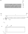
- FIG. 1 is a schematic cross-sectional view of a film for an LED backlight according to one embodiment of the present invention.
- a film 110 for an LED backlight according to this embodiment includes a low-refractive index layer 10 and a first pressure-sensitive adhesive layer 20 arranged on at least one side of the low-refractive index layer 10.
- the low-refractive index layer 10 has a refractive index of 1.25 or less.
- the film 110 for an LED backlight may further include a base material 30 as required. In one embodiment, when the film 110 for an LED backlight includes the base material 30, the first pressure-sensitive adhesive layer 20, the low-refractive index layer 10, and the base material 30 are arranged in the stated order.
- the base material 30 is arranged so as to be peelable from the low-refractive index layer 10.
- the film 110 for an LED backlight further includes a second pressure-sensitive adhesive layer 40 as required.
- the film 110 for an LED backlight includes the second pressure-sensitive adhesive layer 40, the first pressure-sensitive adhesive layer 20, the low-refractive index layer 10, the base material 30, and the second pressure-sensitive adhesive layer 40 are arranged in the stated order.
- each constituent member in the drawings is schematically illustrated, and the size and/or scale thereof in the illustration is different from the actual size and/or scale thereof.
- FIG. 2(a) is a schematic cross-sectional view of a light guide unit according to one embodiment of the present invention
- FIG. 2(b) is a schematic plan view of the light guide unit of FIG. 2(a).
- FIG. 2(b) is a view of a light guide unit 100 of FIG. 2(a) seen from below (lower side of the drawing sheet) .
- the light guide unit 100 includes the film 110 for an LED backlight and a light guide plate 120.
- the film 110 for an LED backlight of the present invention may be used by being bonded to part of a main surface of the light guide plate 120.
- the film 110 for an LED backlight may be used by being bonded in the vicinity of an end surface 121 of the light guide plate 120 in its light guiding direction (end surface 121 on which a light source is to be arranged) .
- the film 110 for a LED backlight film may be preferably used by being bonded to the light guide plate 120 so as to cover part of one surface of the light guide plate 120 in a light guiding direction X, and so as to cover the entirety of the one surface of the light guide plate 120 in a direction Y perpendicular to the light guiding direction X in a plane including the light guiding direction X.
- the film 110 for an LED backlight may be bonded in such a manner that the light guide plate 120 and the low-refractive index layer 10 are arranged via the first pressure-sensitive adhesive layer 20.
- the film 110 for an LED backlight is preferably directly arranged on the light guide plate.
- the film 110 for an LED backlight includes the base material 30, the film 110 for an LED backlight is preferably directly arranged in such a manner that the low-refractive index layer 10 is arranged inside (light guide plate side) with respect to the base material 30.
- the light guide unit 100 may be applied to a sidelight-type planar backlight.
- the light guide unit 100 may be used with an LED light source 130 being arranged on the end surface 121 of the light guide plate 120, and constitute an LED backlight 200 together with the LED light source 130 ( FIG. 3 ).
- the term "light guiding direction" means a direction perpendicular to the end surface on which the light source is to be arranged.
- the light guide plate can be fixed to the main body of the LED backlight.
- light can be satisfactorily reflected at an interface between the light guide plate and the film for an LED backlight, and hence an improvement in waveguide efficiency of light can be achieved.
- the emitted light intensity of the light guide plate as a whole can be enhanced.
- the film for an LED backlight of the present invention is used as described above, light leakage in the vicinity of the entrance surface of the light guide plate and unevenness in lightness can be prevented.
- positioning of the light guide plate can be performed, and hence a positional relationship between the LED light source and the light guide plate can be easily made proper.
- the thickness of the film for an LED backlight is preferably 120 ⁇ m or less, more preferably 110 ⁇ m or less, still more preferably 100 ⁇ m or less, particularly preferably 60 ⁇ m or less. When the thickness falls within such ranges, in the application of the film for an LED backlight to a backlight, the positional relationship between the LED light source and the light guide plate can be appropriately adjusted.
- the thickness of the film for an LED backlight may be set to an appropriate thickness depending on the form of the backlight to which the film for an LED backlight is applied. The lower limit of the thickness of the film for an LED backlight is, for example, 10 ⁇ m.
- the film for an LED backlight has a heat resistance of preferably 60°C or more, more preferably 80°C or more. When the heat resistance falls within such ranges, there can be obtained a film for an LED backlight, which is suited for use in the vicinity of an LED light source and can satisfactorily maintain the above-mentioned effect.
- the "heat resistance” means that, when the film for an LED backlight is placed in an oven at 60° or 80°C or more for 300 hours or more, changes in characteristics (emitted light quantity, directivity, and adhesion strength for a layer with which the film for an LED backlight is brought into direct contact) after the placement in the oven as compared to those therebefore fall within ranges in which use for an LED backlight is not affected.
- the low-refractive index layer has a refractive index of 1.25 or less.
- a film for an LED backlight including a low-refractive index layer having such refractive index is laminated on the light guide plate, there can be obtained an LED backlight capable of satisfactorily reflecting light at the interface between the light guide plate and the film for an LED backlight, thereby being excellent in waveguide efficiency of light and excellent in emission intensity.
- the refractive index of the low-refractive index layer is preferably 1.20 or less, more preferably 1.18 or less, still more preferably 1.15 or less.
- the refractive index of the low-refractive index layer is preferably as low as possible, but the lower limit thereof is, for example, 1.07 or more (preferably 1.05 or more).
- the term "refractive index" refers to a refractive index measured at a wavelength of 550 nm.
- the thickness of the low-refractive index layer is preferably from 0.01 ⁇ m to 100 ⁇ m, more preferably from 0.05 ⁇ m to 70 ⁇ m, still more preferably from 0.1 ⁇ m to 48 ⁇ m, particularly preferably from 0.3 ⁇ m to 40 ⁇ m, most preferably from 0.3 ⁇ m to 30 ⁇ m.
- the low-refractive index layer may have any appropriate form as long as its refractive index falls within the above-mentioned ranges.
- the low-refractive index layer is configured to be a porous body having predetermined voids.
- the void ratio of the low-refractive index layer configured to be a porous body is preferably from 5 vol% to 95 vol%, more preferably from 15 vol% to 95 vol%, still more preferably from 25 vol% to 90 vol%, still more preferably from 35 vol% to 90 vol%, particularly preferably from 38 vol% to 85 vol%, most preferably from 40 vol% to 80 vol%.
- a low-refractive index layer having a particularly low refractive index can be formed.
- a ratio (volume ratio) between a material forming the layer and air may be calculated by a conventional method (involving, for example, measuring the weight and volume of the layer and calculating the density thereof), and hence the void ratio (vol%) may be thus calculated.
- the refractive index and the void ratio correlate with each other, and hence, for example, the void ratio may also be calculated from the value of the refractive index as a layer.
- the void ratio is calculated by Lorentz-Lorenz's formula from the value of the refractive index measured with an ellipsometer.
- the size of each of the voids is preferably from 2 nm to 500 nm, more preferably from 5 nm to 500 nm, still more preferably from 10 nm to 200 nm, particularly preferably from 20 nm to 100 nm.
- the size of each of the voids may be measured by a BET test method.
- the void size may be evaluated from a pore distribution obtained by: loading 0.1 g of a low-refractive index layer sample into a capillary of a specific surface area measurement apparatus (product name: "ASAP2020", manufactured by Micromeritics Instrument Corporation); then removing gas in its void structure through drying under reduced pressure at room temperature for 24 hours; and then adsorbing a nitrogen gas onto the low-refractive index layer sample.
- a specific surface area measurement apparatus product name: "ASAP2020”, manufactured by Micromeritics Instrument Corporation
- the peak pore diameter of the low-refractive index layer configured to be a porous body is preferably from 5 nm to 50 nm, more preferably from 10 nm to 40 nm, still more preferably from 20 nm to 30 nm.
- the peak pore diameter is determined from a BJH plot and a BET plot, and an isothermal adsorption curve, each of which is based on nitrogen adsorption, through use of a pore distribution/specific surface area measurement apparatus (product name: "BELLSORP MINI", from MicrotracBEL Corp.).
- the low-refractive index layer configured to be a porous body contains, for example, approximately spherical particles, such as silicone particles, silicone particles having fine pores, or silica hollow nanoparticles, fibrous particles, such as a cellulose nanofiber, an alumina nanofiber, or a silica nanofiber, or flat plate-like particles, such as nanoclay formed of bentonite.
- the low-refractive index layer configured to be a porous body is a porous body formed by chemical bonding between particles.
- the particles forming the low-refractive index layer configured to be a porous body may be bonded to each other via a small amount of a binder component (e.g., a binder component having a weight equal to or smaller than that of the particles).
- a binder component e.g., a binder component having a weight equal to or smaller than that of the particles.
- the void ratio and refractive index of the low-refractive index layer configured to be a porous body may be adjusted on the basis of, for example, the particle diameters and particle diameter distribution of the particles forming the low-refractive index layer.
- the low-refractive index layer configured to be a porous body there are given, for example, methods described in JP 2010-189212 A , JP 2008-040171 A , JP 2006-011175 A , WO 2004/113966 A1 , and references thereof.
- the low-refractive index layer may be produced by any production method, which is not limited to the above-mentioned production methods.
- the low-refractive index layer is preferably a silicone porous body.
- the silicone porous body may be formed of fine porous particles of a silicon compound that are bonded to each other.
- An example of the fine porous particles of a silicon compound is a pulverized product of a gelled silicon compound.
- the silicone porous body may be formed by, for example, applying an application liquid containing the pulverized product of a gelled silicon compound to a base material.
- the pulverized product of a gelled silicon compound may be subjected to, for example, the action of a catalyst, light irradiation, or heating, to form a chemical bond (e.g., a siloxane bond).
- silicon compound is a compound represented by the following formula (1).
- R 1 represents preferably a linear or branched alkyl group having 1 to 6 carbon atoms, more preferably a linear or branched alkyl group having 1 to 4 carbon atoms, still more preferably an alkyl group having 1 or 2 carbon atoms.
- R 2 represents preferably a hydrogen atom or a linear or branched alkyl group having 1 to 6 carbon atoms, more preferably a hydrogen atom or a linear or branched alkyl group having 1 to 4 carbon atoms, still more preferably a hydrogen atom or an alkyl group having 1 or 2 carbon atoms.
- silicon compound examples include tris(hydroxy)methylsilane and trimethoxy(methyl)silane.
- the silicon compound is a trifunctional silane.
- a low-refractive index layer having a particularly low refractive index can be formed.
- the silicon compound is a tetrafunctional silane. When the tetrafunctional silane is used, a low-refractive index layer excellent in scratch resistance can be formed.
- the gelation of the silicon compound may be performed by, for example, a dehydration condensation reaction of the silicon compound. Any appropriate method may be adopted as a method for the dehydration condensation reaction.
- pulverization method for the gelled silicon compound.
- An example of the pulverization method is a method involving using a pulverization apparatus making use of a cavitation phenomenon, such as an ultrasonic homogenizer or a high-speed rotating homogenizer.
- the volume-average particle diameter of the fine porous particles of a silicon compound is preferably from 0.1 ⁇ m to 2 ⁇ m, more preferably from 0.2 ⁇ m to 1.5 ⁇ m, still more preferably from 0.4 ⁇ m to 1 ⁇ m.
- the volume-average particle diameter may be measured by a dynamic light scattering method.
- the ratio of particles each having a particle diameter of from 0.4 ⁇ m to 1 ⁇ m to all particles is preferably from 50 wt% to 99.9 wt%, more preferably from 80 wt% to 99.8 wt%, still more preferably from 90 wt% to 99.7 wt%.
- the ratio of particles each having a particle diameter of from 1 ⁇ m to 2 ⁇ m to all particles is preferably from 0.1 wt% to 50 wt%, more preferably from 0.2 wt% to 20 wt%, still more preferably from 0.3 wt% to 10 wt%.
- the particle size distribution may be measured with a particle size distribution evaluation apparatus.
- the base material may be formed of any appropriate material.
- a material for forming the base material there are given, for example: thermoplastic resins, such as a polyethylene terephthalate-based resin, an acrylic resin, a cellulose-based resin, a cycloolefin-based resin, and an olefin-based resin; thermosetting resins; inorganic materials, such as glass and silicon; and carbon fiber materials.
- the thickness of the base material is not particularly limited, and may be set to any appropriate thickness depending on applications.
- the thickness of the base material is, for example, from 1 ⁇ m to 100 ⁇ m, preferably from 1 ⁇ m to 60 ⁇ m, more preferably from 2 ⁇ m to 40 ⁇ m.
- the base material may be transparent, or may be non-transparent.
- the base material is transparent.
- its transmittance is preferably from 50% to 99%, more preferably from 60% to 99%, still more preferably from 70% to 99%.
- the transmittance falls within such ranges, there can be obtained a film for an LED backlight, which can enable appropriate guiding of light, even in the case where light leakage to the base material occurs.
- the first pressure-sensitive adhesive layer contains any appropriate pressure-sensitive adhesive.
- the pressure-sensitive adhesive preferably has transparency and optical isotropy.
- Specific examples of the pressure-sensitive adhesive include a rubber-based pressure-sensitive adhesive, an acrylic pressure-sensitive adhesive, a silicone-based pressure-sensitive adhesive, an epoxy-based pressure-sensitive adhesive, and a cellulose-based pressure-sensitive adhesive. Of those, a rubber-based pressure-sensitive adhesive or an acrylic pressure-sensitive adhesive is preferred.
- the acrylic pressure-sensitive adhesive is used as the pressure-sensitive adhesive.
- An example of the acrylic pressure-sensitive adhesive is an acrylic pressure-sensitive adhesive including as a base polymer an acrylic polymer (homopolymer or copolymer) containing a constituent unit derived from an alkyl (meth)acrylate.
- the alkyl group of the alkyl (meth) acrylate has, for example, 2 to 18 carbon atoms.
- the alkyl group may be linear or branched.
- the number of carbon atoms of the alkyl group is preferably from 2 to 14, more preferably from 3 to 12, still more preferably from 4 to 9.
- alkyl (meth)acrylate examples include ethyl (meth)acrylate, n-butyl (meth)acrylate, s-butyl (meth)acrylate, t-butyl (meth)acrylate, isobutyl (meth)acrylate, n-pentyl (meth)acrylate, isopentyl (meth)acrylate, hexyl (meth)acrylate, heptyl (meth)acrylate, isoamyl (meth)acrylate, 2-ethylhexyl (meth)acrylate, n-octyl (meth)acrylate, isooctyl (meth)acrylate, n-nonyl (meth)acrylate, isononyl (meth)acrylate, n-decyl (meth)acrylate, isodecyl (meth)acrylate, n-dodecyl (meth)acrylate, iso
- the content ratio of the constituent unit derived from an alkyl (meth)acrylate is preferably from 30 parts by weight to 100 parts by weight, more preferably from 85 parts by weight to 99.99 parts by weight, still preferably from 90 parts by weight to 99.95 parts by weight, particularly preferably from 95 parts by weight to 99 parts by weight with respect to 100 parts by weight of the acrylic polymer.
- a pressure-sensitive adhesive layer excellent in pressure-sensitive adhesive property can be formed.
- the acrylic polymer further has a constituent unit derived from a functional group-containing monomer .
- a monomer having any appropriate functional group may be used as the functional group-containing monomer.
- Specific examples of the functional group-containing monomer include a carboxyl group-containing monomer, a hydroxyl group-containing monomer, an amide group-containing monomer, and an amino group-containing monomer. When any such monomer is used, a pressure-sensitive adhesive layer excellent in heat resistance can be formed.
- the functional group-containing monomers may be used alone or in combination thereof.
- a monomer having a polymerizable functional group having an unsaturated double bond, such as a (meth)acryloyl group or a vinyl group, and a carboxyl group may be used as the carboxyl group-containing monomer.
- the carboxyl group-containing monomer include (meth)acrylic acid, carboxyethyl (meth)acrylate, carboxypentyl (meth)acrylate, itaconic acid, maleic acid, fumaric acid, and crotonic acid. Of those, (meth) acrylic acid is preferred, and acrylic acid is particularly preferred.
- a monomer having a polymerizable functional group having an unsaturated double bond, such as a (meth)acryloyl group or a vinyl group, and a hydroxyl group may be used as the hydroxyl group-containing monomer.
- the hydroxyl group-containing monomer include: hydroxyalkyl (meth)acrylates, such as 2-hydroxyethyl (meth)acrylate, 2-hydroxybutyl (meth)acrylate, 3-hydroxypropyl (meth)acrylate, 4-hydroxybutyl (meth)acrylate, 6-hydroxyhexyl (meth)acrylate, 8-hydroxyoctyl (meth)acrylate, 10-hydroxydecyl (meth)acrylate, and 12-hydroxylauryl (meth)acrylate; and hydroxyethyl(meth)acrylamide, N-methylol(meth)acrylamide, and besides, (4-hydroxymethylcyclohexyl)methyl acrylate, N-methylol(meth)acrylamide, N-hydroxy(meth
- a monomer having a polymerizable functional group having an unsaturated double bond, such as a (meth)acryloyl group or a vinyl group, and an amide bond may be used as the amide group-containing monomer.
- the amide group-containing monomer include (meth)acrylamide, N-substituted amide-based monomers, such as N,N-dimethyl(meth)acrylamide, N,N-diethyl(meth)acrylamide, N,N-diethylmethacrylamide, N-isopropyl(meth)acrylamide, N-methoxymethyl(meth)acrylamide, N-butoxymethyl(meth)acrylamide, N-vinylcaprolactam, N-acryloylmorpholine, N-acryloylpiperidine, N-methacryloylpiperidine, and N-acryloylpyrrolidine, diacetone (meth)acrylamide, and N-vinylacetamide.
- a monomer having a (meth)acryloyl group and an amino group may be used as the amino group-containing monomer.
- the amino group-containing monomer is preferably a monomer having a tertiary amino group.
- the tertiary amino group is preferably a tertiary aminoalkyl group. Examples of such tertiary amino group-containing monomer include an N,N-dialkylaminoalkyl(meth)acrylamide and an N,N-dialkylaminoalkyl (meth)acrylate.
- tertiary amino group-containing monomer examples include N,N-dimethylaminoethyl(meth)acrylamide, N,N-dimethylaminopropyl(meth)acrylamide, N,N-diethylaminoethyl(meth)acrylamide, N,N-diethylaminopropyl(meth)acrylamide, N,N-dimethylaminoethyl (meth)acrylate, N,N-dimethylaminopropyl (meth)acrylate, N,N-diethylaminoethyl (meth)acrylate, and N,N-diethylaminopropyl(meth)acrylamide.
- a monomer having a secondary amino group there is given, for example, t-butylaminoethyl (meth)acrylate.
- the content ratio of the constituent unit derived from a functional group-containing monomer is preferably from 0.01 part by weight to 15 parts by weight, more preferably from 0.05 part by weight to 10 parts by weight with respect to 100 parts by weight of the (meth)acrylic polymer.
- the acrylic polymer may have a constituent unit derived from any appropriate other monomer as required.
- the other monomer include: aromatic ring-containing monomers, such as phenoxyethyl (meth)acrylate, benzyl (meth)acrylate, phenol ethylene oxide-modified (meth)acrylate, 2-naphthoethyl (meth)acrylate, 2-(4-methoxy-1-naphthoxy)ethyl (meth)acrylate, phenoxypropyl (meth)acrylate, phenoxydiethylene glycol (meth)acrylate, polystyryl (meth)acrylate, and styrene; vinyl ester-based monomers, such as vinyl acetate and vinyl propionate; and alkoxyalkyl (meth) acrylate-basedmonomers, such as methoxyethyl (meth)acrylate and ethoxyethyl (meth)acrylate.
- aromatic ring-containing monomers such as
- the weight-average molecular weight of the acrylic polymer is preferably from 1,000,000 to 3,000,000, more preferably from 1,500,000 to 2,500,000, still more preferably from 1,700,000 to 2,500,000.
- the weight-average molecular weight refers to a value measured by gel permeation chromatography (GPC) and calculated in terms of polystyrene.
- the pressure-sensitive adhesive may further contain any appropriate additive as required.
- the additive include a cross-linking agent, a pigment, a dye, a surfactant, a plasticizer, a tackifier, a surface lubricant, a leveling agent, a softener, an antioxidant, an age resistor, a light stabilizer, a UV absorber, a polymerization inhibitor, and an inorganic or organic filler.
- the cross-linking agent include an isocyanate-based cross-linking agent, an epoxy-based cross-linking agent, a peroxide-based cross-linking agent, a metal chelate-based cross-linking agent, and an oxazoline-based cross-linking agent.
- an isocyanate-based cross-linking agent is preferred.
- the content of the cross-linking agent is preferably 2 parts by weight or less, more preferably 1.5 parts by weight or less, still more preferably 1 part by weight or less with respect to 100 parts by weight of the acrylic polymer.
- the thickness of the first pressure-sensitive adhesive layer is preferably from 0.1 ⁇ m to 100 ⁇ m, more preferably from 5 ⁇ m to 50 ⁇ m, still more preferably from 5 ⁇ m to 25 ⁇ m.
- the refractive index of the first pressure-sensitive adhesive layer is from 1.42 to 1.60, more preferably from 1.47 to 1.58. When the refractive index falls within such ranges, an LED backlight excellent in waveguide efficiency of light and excellent in emission intensity can be obtained.
- the light transmittance of the first pressure-sensitive adhesive layer is preferably from 85% to 99%, more preferably from 88% to 99%, still more preferably from 90% to 99%.
- the haze value of the first pressure-sensitive adhesive layer is preferably 5 or less, more preferably 3 or less, still more preferably 1 or less.
- the first pressure-sensitive adhesive layer is preferably bonded to a light guide plate side in each of a light guide unit and an LED backlight.
- the first pressure-sensitive adhesive layer is brought into close contact with the light guide plate directly or indirectly via a resin layer directly laminated on the light guide plate.
- the pressure-sensitive adhesive strength of the first pressure-sensitive adhesive layer for a layer adjacent to the opposite side of the first pressure-sensitive adhesive layer to the low-refractive index layer is preferably 0.8 N/25 mm or more, more preferably 1 N/25 mm or more, still more preferably 1.5 N/25 mm or more.
- the upper limit of the pressure-sensitive adhesive strength is, for example, 30 N/25 mm.
- pressure-sensitive adhesive strength refers to a pressure-sensitive adhesive strength measured under an environment at 23°C by a method in conformity with JIS Z 0237:2000 (bonding condition: 1 pass back and forth with a 2 kg roller, peel rate: 300 mm/min, peel angle: 180°).
- the second pressure-sensitive adhesive layer contains any appropriate pressure-sensitive adhesive.
- the pressure-sensitive adhesive preferably has transparency and optical isotropy.
- Specific examples of the pressure-sensitive adhesive include a rubber-based pressure-sensitive adhesive, an acrylic pressure-sensitive adhesive, a silicone-based pressure-sensitive adhesive, an epoxy-based pressure-sensitive adhesive, and a cellulose-based pressure-sensitive adhesive. Of those, a rubber-based pressure-sensitive adhesive or an acrylic pressure-sensitive adhesive is preferred.
- the acrylic pressure-sensitive adhesive described in the section A-4 may be used.
- the thickness of the second pressure-sensitive adhesive layer is preferably from 0.1 ⁇ m to 100 ⁇ m, more preferably from 5 ⁇ m to 50 ⁇ m, still more preferably from 5 ⁇ m to 25 ⁇ m.
- the second pressure-sensitive adhesive layer is preferably bonded to a flexible substrate (flexible printed circuit: FPC) in each of a light guide unit and an LED backlight.
- FPC flexible printed circuit
- the second pressure-sensitive adhesive layer is brought into close contact with the FPC directly or indirectly via a resin layer, an insulating layer, or the like directly laminated on the FPC.
- the pressure-sensitive adhesive strength of the second pressure-sensitive adhesive layer for a layer adjacent to the opposite side of the second pressure-sensitive adhesive layer to the low-refractive index layer is preferably 0.5 N/25 mm or more, more preferably 0.7 N/25 mm or more, still more preferably 1.0 N/25 mm or more.
- the upper limit of the pressure-sensitive adhesive strength is, for example, 30 N/25 mm.
- the second pressure-sensitive adhesive layer may be transparent, or may be non-transparent. In one embodiment, the second pressure-sensitive adhesive layer is transparent. When the second pressure-sensitive adhesive layer is transparent, its transmittance is preferably from 50% to 99%, more preferably from 60% to 99%, still more preferably from 70% to 99%. When the transmittance falls within such ranges, there can be obtained a film for an LED backlight, which can enable appropriate guiding of light, even in the case where light leakage occurs beyond the low-refractive index layer.
- the film for an LED backlight may be produced by any appropriate method.
- the low-refractive index layer may be formed on the base material by applying an application liquid for forming a low-refractive index layer containing predetermined particles (e.g., the fine porous particles of a silicon compound, preferably the pulverized product of a gelled silicon compound) onto the base material, followed by drying.
- predetermined particles e.g., the fine porous particles of a silicon compound, preferably the pulverized product of a gelled silicon compound
- the application liquid for forming a low-refractive index layer contains any appropriate solvent.
- the solvent include isopropyl alcohol, ethanol, methanol, n-butanol, 2-butanol, isobutyl alcohol, and pentanol.
- the application liquid for forming a low-refractive index layer further contains a catalyst.
- a catalyst capable of promoting the chemical bonding of the particles is used as the catalyst.
- the catalyst include: base catalysts, such as potassium hydroxide, sodium hydroxide, and ammonium hydroxide; and acid catalysts, such as hydrochloric acid, acetic acid, and oxalic acid. Of those, a base catalyst is preferred.
- the content ratio of the catalyst is preferably from 0.01 part by weight to 20 parts by weight, more preferably from 0.1 part by weight to 5 parts by weight with respect to 100 parts by weight of the particles in the application liquid for forming a low-refractive index layer.
- any appropriate method may be adopted as an application method for the application liquid for forming a low-refractive index layer.
- the application method include bar coater coating, air knife coating, gravure coating, gravure reverse coating, reverse roll coating, lip coating, die coating, and dip coating.
- drying method for the application liquid for forming a low-refractive index layer may be natural drying, drying by heating, or drying under reduced pressure.
- heating means there are given, for example, a hot air fan, a heating roll, and a far-infrared heater.
- the applied layer may be subjected to heating treatment.
- the heating treatment can promote bonding between the particles forming the low-refractive index layer.
- a heating temperature is preferably 200°C or more.
- the drying step may double as the heating treatment.
- the first pressure-sensitive adhesive layer and the second pressure-sensitive adhesive layer may each be formed by any appropriate method.
- the first pressure-sensitive adhesive layer and the second pressure-sensitive adhesive layer may each be formed by applying a pressure-sensitive adhesive by a method such as bar coater coating, air knife coating, gravure coating, gravure reverse coating, reverse roll coating, lip coating, die coating, or dip coating.
- the first pressure-sensitive adhesive layer and the second pressure-sensitive adhesive layer may each be formed by a method involving transferring a pressure-sensitive adhesive layer formed on a release liner.
- the pressure-sensitive adhesive after its application may be irradiated with an active energy ray (preferably UV light) .
- the irradiation dose of an electron beam is preferably from 2 kGy to 100 kGy, more preferably from 2 kGy to 70 kGy, still more preferably from 5 kGy to 50 kGy.
- a light guide unit of the present invention includes the film 110 for an LED backlight and the light guide plate 120.
- the film 110 for an LED backlight is arranged by being laminated on part of one surface of the light guide plate 120. More specifically, the film 110 for an LEDbacklight is arranged by being bonded in the vicinity of the end surface 121 of the light guide plate 120 in its light guiding direction (end surface 121 on which a light source is to be arranged) .
- the film 110 for a LED backlight may be preferably bonded to the light guide plate 120 so as to cover part of one surface 122 of the light guide plate 120 in the light guiding direction X of the light guide plate 120, and so as to cover the entirety of the one surface 122 of the light guide plate 120 in the direction Y perpendicular to the light guiding direction X in a plane including the light guiding direction X.
- the film 110 for an LED backlight may be bonded in such a manner that the light guide plate and the low-refractive index layer are arranged via the first pressure-sensitive adhesive layer.
- the film 110 for an LED backlight is preferably directly arranged on the light guide plate.
- the film 110 for an LED backlight when the film 110 for an LED backlight includes the base material, the film 110 for an LED backlight is preferably directly arranged on the light guide plate in such a manner that the low-refractive index layer is arranged inside (light guide plate side) with respect to the base material.
- the term "directly arranged" means that the film 110 for an LED backlight and the light guide plate 120 are arranged without any other layer arranged between the film 110 for an LED backlight and the light guide plate 120.
- the surface of the light guide plate to which the film for an LED backlight is bonded corresponds to the surface of the light guide plate on the opposite side to its light emission surface when the light guide unit is applied to an LED backlight.
- the film for an LED backlight may be arranged in such a manner that one end portion thereof is brought into contact with the end surface of the light guide plate, or may be arranged at a slight distance from the end surface of the light guide plate.
- the distance by which the film for an LED backlight is separated from the light guide plate is preferably 5 mm or less, more preferably 3 mm or less, particularly preferably 1 mm or less.
- a length Lx of the film for an LED backlight in the light guiding direction is preferably 10 mm or less, more preferably 8 mmorless, still more preferably 5 mm or less, particularly preferably 3 mm or less.
- the lower limit of the length Lx is, for example, 0.5 mm.
- a ratio (Lx/L) between the length Lx of the film for an LED backlight in the light guiding direction and a length L of the light guide plate in the light guiding direction is preferably from 1/3,000 to 1/10, more preferably from 1/1,000 to 1/20. In the present invention, light can be satisfactorily reflected in the vicinity of the entrance surface to enhance the emitted light intensity of the light guide plate as a whole.
- the film for an LED backlight may be applied to a region of the light guide plate where light emission is not performed.
- any appropriate material may be used as a material for forming the light guide plate as long as light radiated from the LED light source can be efficiently guided.
- the material for forming the light guide plate include an acrylic resin, a polycarbonate-based resin, and a cycloolefin-based resin.
- the thickness of the light guide plate is, for example, from 100 ⁇ m to 2,000 ⁇ m.
- the refractive index of the light guide plate is preferably 1.4 or more, more preferably more than 1.45, still more preferably more than 1.45 and 2 or less, particularly preferably from 1.48 to 1.8.
- a difference between the refractive index of the light guide plate and the refractive index of the low-refractive index layer is preferably 0.2 or more, more preferably 0.23 or more, still more preferably 0.25 or more.
- the difference falls within such ranges, there can be obtained an LED backlight unit capable of satisfactorily reflecting light at the interface between the light guide plate and the film for an LED backlight, thereby being excellent in waveguide efficiency of light and excellent in emission intensity.
- the refractive index of the light guide plate is higher than the refractive index of the low-refractive index layer.
- FIG. 3 is a schematic cross-sectional view of an LED backlight according to one embodiment of the present invention.
- the LED backlight 200 may include the light guide unit 100 and the LED light source 130 arranged on the end surface 121 of the light guide plate 120 included in the light guide unit 100 on the side on which the film 110 for an LED backlight is arranged.
- the thickness of the film for an LED backlight is preferably equal to or smaller than (thickness of LED light source-thickness of light guide plate). More specifically, the thickness of the film for an LED backlight is preferably from ⁇ (thickness of LED light source-thickness of light guide plate) ⁇ 10% ⁇ to ⁇ (thickness of LED light source-thickness of light guide plate) ⁇ 100% ⁇ , more preferably from ⁇ (thickness of LED light source-thickness of light guide plate) ⁇ 30% ⁇ to ⁇ (thickness of LED light source-thickness of light guide plate) ⁇ 100% ⁇ , still more preferably from ⁇ (thickness of LED light source-thickness of light guide plate) ⁇ 50% ⁇ to ⁇ (thickness of LED light source-thickness of light guide plate) ⁇ 100% ⁇ .
- the thickness of the LED light source is generally from 200
- the LED backlight may include any appropriate other member.
- the LED backlight 200 may further include a reflective plate 140 arranged via an air layer on a surface of the light guide plate 120 on which the film 110 for an LED backlight is not arranged.
- a flexible substrate 150 for an LED may be arranged beneath the film 110 for an LED backlight (opposite side to the light guide plate 120 ).
- the flexible substrate for an LED may include a colored layer (e.g., a white-colored ink layer) on its surface on the side of the film for an LED backlight.
- the LED backlight 200 may include a chassis 160 configured to receive the above-mentioned members.
- a low-refractive index layer was cut into a size of 50 mm ⁇ 50 mm, and the resultant was bonded to the front surface of a glass plate (thickness: 3 mm) via a pressure-sensitive adhesion layer.
- a central portion (diameter: about 20 mm) of the back surface of the glass plate was painted over with a black felt-tip pen to provide a sample prevented from reflection at the back surface of the glass plate.
- the sample was set in an ellipsometer (manufactured by J.A. Woollam Japan: VASE), and its refractive index was measured under the conditions of a wavelength of 500 nm and an incident angle of from 50° to 80°.
- a white color was displayed on the entire screen of a liquid crystal display apparatus, and its front brightness (white brightness) wasmeasured (unit: cd/m 2 ) with a conoscope (manufactured by Autronic-Melchers GmbH).
- a film for an LED backlight obtained in each of Example and Comparative Example was, as illustrated in FIG. 3 , incorporated into an LED backlight (refractive index of light guide plate: 1.49, thickness of LED light source: 300 ⁇ m), and lightness unevenness of the emission surface of the light guide plate at a time when the LED light source was turned on was visually observed.
- a case in which uniform lighting was able to be performed was defined as acceptable (" ⁇ " in Table 1), and a case in which lightness unevenness and light leakage were able to be observed was defined as unacceptable (“ ⁇ " in Table 1).
- a mixed liquid A 0.95 g of MTMS serving as a precursor of a silicon compound was dissolved in 2.2 g of DMSO to prepare a mixed liquid A.
- a mixed liquid B 0.5 g of a 0.01 mol/L oxalic acid aqueous solution was added, and the mixture was stirred at room temperature for 30 minutes to hydrolyze MTMS.
- a mixed liquid B containing tris(hydroxy)methylsilane was produced.
- the mixed liquid C containing the gelled silicon compound prepared as described above was subjected as it was to maturation treatment by being incubated at 40°C for 20 hours.
- the gelled silicon compound subjected to maturation treatment as described above was crushed using a spatula into granules each having a size of from several mm to several cm. Then, 40 g of IBA was added to the mixed liquid C, and the whole was lightly stirred and then left to stand still at room temperature for 6 hours to decant the solvent and the catalyst in the gel. Similar decantation treatment was performed three times to perform solvent replacement, to thereby provide a mixed liquid D. Then, the gelled silicon compound in the mixed liquid D was subjected to pulverization treatment (high-pressure media-less pulverization).
- the pulverization treatment (high-pressure media-less pulverization) was performed by weighing 1.85 g of the gelled compound in the mixed liquid D' and 1.15 g of IBA into a 5 cc screw-capped vial and then pulverizing the contents under the conditions of 50 W and 20 kHz for 2 minutes through use of a homogenizer (manufactured by SMT Co., Ltd., product name: "UH-50").
- the gelled silicon compound in the mixed liquid D was pulverized, and thus the mixed liquid D' became a sol liquid of a pulverized product.
- a volume-average particle diameter indicating a variation in particle size of the pulverized product contained in the mixed liquid D' was found to be from 0.50 to 0.70 with a dynamic light scattering Nanotrac particle size analyzer (manufactured by Nikkiso Co., Ltd., model UPA-EX150) .
- a solution of a photobase generator (Wako Pure Chemical Industries, Ltd.: product name: WPBG-266) in methyl ethyl ketone (MEK) at a concentration of 1.5 wt% and a solution of bis(trimethoxysilyl)ethane in MEK at a concentration of 5% were added at a ratio of 0.062 g:0.036 g to provide an application liquid for a low-refractive index layer.
- a four-necked flask with a stirring blade, a temperature gauge, a nitrogen gas inlet tube, and a condenser was loaded with 90.7 parts of butyl acrylate, 6 parts of N-acryloylmorpholine, 3 parts of acrylic acid, 0.3 part of 2-hydroxybutyl acrylate, and 0.1 part by weight of 2,2'-azobisisobutyronitrile serving as a polymerization initiator together with 100 g of ethyl acetate. While the contents were gently stirred, a nitrogen gas was introduced to perform nitrogen purge. After that, with the liquid temperature in the flask being kept around 55°C, a polymerization reaction was performed for 8 hours to prepare an acrylic polymer solution.
- an isocyanate cross-linking agent CORONATE L manufactured by Nippon Polyurethane Industry Co., Ltd., tolylene diisocyanate adduct of trimethylolpropane
- benzoyl peroxide NYPER BMT manufactured by Nippon Oil & Fats Co., Ltd.
- ⁇ -glycidoxypropylmethoxysilane manufactured by Shin-Etsu Chemical Co., Ltd.: KBM-403
- the acrylic pressure-sensitive adhesive solution was applied to one surface of a silicone-treated polyethylene terephthalate (PET) film (manufactured by Mitsubishi Polyester Film Corporation, thickness: 38 ⁇ m) so that a pressure-sensitive adhesive layer after drying had a thickness of 10 ⁇ m, and the applied solution was dried at 150°C for 3 minutes to form the first pressure-sensitive adhesive layer.
- PET polyethylene terephthalate
- a four-necked flask with a stirring blade, a temperature gauge, a nitrogen gas inlet tube, and a condenser was loaded with 97 parts of butyl acrylate, 3 parts of acrylic acid, 1 part of 2-hydroxybutyl acrylate, and 0.1 part by weight of 2,2'-azobisisobutyronitrile serving as a polymerization initiator together with 100 g of ethyl acetate. While the contents were gently stirred, a nitrogen gas was introduced to perform nitrogen purge. After that, with the liquid temperature in the flask being kept around 55°C, a polymerization reaction was performed for 8 hours to prepare an acrylic polymer solution.
- an isocyanate cross-linking agent CORONATE L manufactured by Nippon Polyurethane Industry Co., Ltd., tolylene diisocyanate adduct of trimethylolpropane
- benzoyl peroxide NYPER BMT manufactured by Nippon Oil & Fats Co., Ltd.
- ⁇ -glycidoxypropylmethoxysilane manufactured by Shin-Etsu Chemical Co., Ltd.: KBM-403
- the acrylic pressure-sensitive adhesive solution was applied to one surface of a silicone-treated polyethylene terephthalate (PET) film (manufactured by Mitsubishi Polyester Film Corporation, thickness: 38 ⁇ m) so that a pressure-sensitive adhesive layer after drying had a thickness of 15 ⁇ m, and the applied solution was dried at 150°C for 3 minutes to form the second pressure-sensitive adhesive layer.
- PET polyethylene terephthalate
- the application liquid for a low-refractive index layer prepared in Production Example 1 was applied to an acrylic resin film (thickness: 20 ⁇ m) serving as a base material, and was dried to provide a laminate in which a low-refractive index layer (refractive index: 1.18) having a thickness of 850 nm was arranged on one surface of the base material.
- the low-refractive index layer was subjected to UV (300 mJ) irradiation, and then the pressure-sensitive adhesive layer of Production Example 2 (first pressure-sensitive adhesive layer) and the pressure-sensitive adhesive layer of Production Example 3 (second pressure-sensitive adhesive layer) were transferred onto the low-refractive index layer side and base material side of the laminate, respectively, followed by aging at 60°C for 20 hours, to provide a film for an LED backlight (first pressure-sensitive adhesive layer/low-refractive index layer/base material/second pressure-sensitive adhesive layer).
- the pressure-sensitive adhesive layer of Production Example 2 was transferred onto one surface of an acrylic resin film (thickness : 20 ⁇ m) serving as a base material, and the pressure-sensitive adhesive layer of Production Example 3 was transferred onto the other surface, followed by aging at 60°C for 20 hours, to provide a film for an LED backlight (first pressure-sensitive adhesive layer/base material/second pressure-sensitive adhesive layer).
- the use of the film for an LED backlight of the present invention can provide an LED backlight capable of efficiently guiding entering light.
Landscapes
- Physics & Mathematics (AREA)
- Optics & Photonics (AREA)
- Engineering & Computer Science (AREA)
- General Physics & Mathematics (AREA)
- Microelectronics & Electronic Packaging (AREA)
- General Engineering & Computer Science (AREA)
- Planar Illumination Modules (AREA)
Applications Claiming Priority (2)
| Application Number | Priority Date | Filing Date | Title |
|---|---|---|---|
| JP2018017206 | 2018-02-02 | ||
| PCT/JP2019/002036 WO2019151073A1 (ja) | 2018-02-02 | 2019-01-23 | Ledバックライト用フィルム、ledバックライト |
Publications (2)
| Publication Number | Publication Date |
|---|---|
| EP3748221A1 true EP3748221A1 (de) | 2020-12-09 |
| EP3748221A4 EP3748221A4 (de) | 2021-10-13 |
Family
ID=67478722
Family Applications (1)
| Application Number | Title | Priority Date | Filing Date |
|---|---|---|---|
| EP19748048.6A Pending EP3748221A4 (de) | 2018-02-02 | 2019-01-23 | Led-hintergrundbeleuchtungsfolie und led-hintergrundbeleuchtung |
Country Status (7)
| Country | Link |
|---|---|
| US (1) | US20200355866A1 (de) |
| EP (1) | EP3748221A4 (de) |
| JP (2) | JPWO2019151073A1 (de) |
| KR (1) | KR20200118009A (de) |
| CN (1) | CN111656087A (de) |
| TW (1) | TWI846684B (de) |
| WO (1) | WO2019151073A1 (de) |
Cited By (1)
| Publication number | Priority date | Publication date | Assignee | Title |
|---|---|---|---|---|
| WO2024104664A1 (de) * | 2022-11-16 | 2024-05-23 | Webasto SE | Fahrzeugscheibe mit einem verbundaufbau |
Families Citing this family (14)
| Publication number | Priority date | Publication date | Assignee | Title |
|---|---|---|---|---|
| EP4130809A4 (de) | 2020-03-24 | 2024-04-17 | Nitto Denko Corporation | Optisches laminat mit doppelseitiger haftschicht und optische vorrichtung |
| KR102861239B1 (ko) | 2020-03-26 | 2025-09-17 | 닛토덴코 가부시키가이샤 | 광학 부재 그리고 그 광학 부재를 사용한 백라이트 유닛 및 화상 표시 장치 |
| WO2021193896A1 (ja) | 2020-03-27 | 2021-09-30 | 日東電工株式会社 | バックライトユニットおよび画像表示装置 |
| CN115315648B (zh) * | 2020-03-27 | 2026-04-10 | 日东电工株式会社 | 光学构件、以及使用了该光学构件的背光灯单元及图像显示装置 |
| WO2021193894A1 (ja) * | 2020-03-27 | 2021-09-30 | 日東電工株式会社 | 照明装置 |
| TWI877338B (zh) | 2020-03-30 | 2025-03-21 | 日商日東電工股份有限公司 | 背光單元及影像顯示裝置 |
| WO2022265050A1 (ja) | 2021-06-18 | 2022-12-22 | ローム株式会社 | トランスデューサ及び電子機器 |
| JP2023125213A (ja) | 2022-02-28 | 2023-09-07 | 日東電工株式会社 | 積層フィルム |
| US20250172741A1 (en) | 2022-02-28 | 2025-05-29 | Nitto Denko Corporation | Optical member and ar glasses and head-mounted display using said optical member |
| JP2023142896A (ja) | 2022-03-25 | 2023-10-06 | 日東電工株式会社 | 光学積層体 |
| JP2023150234A (ja) * | 2022-03-31 | 2023-10-16 | 日東電工株式会社 | 光学積層体および光学積層体の製造方法 |
| CN115175387B (zh) * | 2022-07-15 | 2025-09-16 | 上海骏珲新材料科技有限公司 | 自限温远红外碳纤维复合面状电热材料及其制备方法 |
| JP2024145876A (ja) | 2023-03-31 | 2024-10-15 | 日東電工株式会社 | 積層体および積層体の製造方法 |
| JP2025059267A (ja) | 2023-09-29 | 2025-04-10 | 日東電工株式会社 | 積層体 |
Family Cites Families (21)
| Publication number | Priority date | Publication date | Assignee | Title |
|---|---|---|---|---|
| JPH03261988A (ja) * | 1990-03-12 | 1991-11-21 | Sumitomo Chem Co Ltd | 面状発光体 |
| JPH09145903A (ja) * | 1995-11-27 | 1997-06-06 | Dainippon Printing Co Ltd | 反射防止フィルム |
| TW200500630A (en) | 2003-06-18 | 2005-01-01 | Asahi Chemical Ind | Antireflective film |
| JP4448392B2 (ja) | 2004-06-28 | 2010-04-07 | Hoya株式会社 | 反射防止膜を有する光学素子の製造方法 |
| US20070264447A1 (en) * | 2004-08-30 | 2007-11-15 | Teijin Dupont Films Japan Limited | Optical Film Laminated Body |
| JP2008040171A (ja) | 2006-08-07 | 2008-02-21 | Pentax Corp | セルフクリーニング効果を有する反射防止膜を設けた光学素子及びその製造方法 |
| JP5007416B2 (ja) | 2009-02-17 | 2012-08-22 | 国立大学法人信州大学 | 多孔質シリカ膜の製造方法 |
| KR20120115568A (ko) * | 2010-02-10 | 2012-10-18 | 쓰리엠 이노베이티브 프로퍼티즈 컴파니 | 점탄성 층을 구비한 조명 장치 |
| JP5652270B2 (ja) * | 2010-03-11 | 2015-01-14 | 三菱化学株式会社 | シリカ系多孔質膜の製造方法 |
| JP6356420B2 (ja) * | 2010-04-14 | 2018-07-11 | スリーエム イノベイティブ プロパティズ カンパニー | パターン付き勾配ポリマーフィルム及び方法 |
| JP2012059645A (ja) * | 2010-09-10 | 2012-03-22 | Fujikura Ltd | 面状発光装置および照明モジュール |
| TWI534458B (zh) * | 2010-10-20 | 2016-05-21 | 3M新設資產公司 | 經保護之低折射率光學元件 |
| JP2012114284A (ja) | 2010-11-25 | 2012-06-14 | Toshiba Corp | Ledモジュール及び照明装置 |
| KR20130028270A (ko) * | 2011-09-09 | 2013-03-19 | 엘지디스플레이 주식회사 | 반사 시트 및 그의 제조방법, 반사 시트를 포함하는 액정표시장치 |
| KR102064751B1 (ko) * | 2014-02-27 | 2020-01-10 | 엘지디스플레이 주식회사 | 베젤이 최소화된 액정표시소자 |
| EP3187927B1 (de) * | 2014-08-28 | 2022-06-29 | Sony Group Corporation | Anzeigevorrichtung und beleuchtungsvorrichtung |
| JP6713871B2 (ja) | 2015-07-31 | 2020-06-24 | 日東電工株式会社 | 光学積層体、光学積層体の製造方法、光学部材、画像表示装置、光学部材の製造方法および画像表示装置の製造方法 |
| JP2017064954A (ja) * | 2015-09-28 | 2017-04-06 | 日東電工株式会社 | 積層フィルムの製造方法および画像表示装置の製造方法 |
| JP6966850B2 (ja) * | 2016-03-18 | 2021-11-17 | 日東電工株式会社 | 光学部材、ならびに、該光学部材を用いたバックライトユニットおよび液晶表示装置 |
| JP6809824B2 (ja) * | 2016-07-04 | 2021-01-06 | 日東電工株式会社 | 光学積層体の製造方法、および光学積層体中間体 |
| TWI587052B (zh) * | 2016-07-18 | 2017-06-11 | 恆顥科技股份有限公司 | 光源模組及顯示裝置 |
-
2019
- 2019-01-23 KR KR1020207021709A patent/KR20200118009A/ko not_active Ceased
- 2019-01-23 JP JP2019569043A patent/JPWO2019151073A1/ja active Pending
- 2019-01-23 EP EP19748048.6A patent/EP3748221A4/de active Pending
- 2019-01-23 WO PCT/JP2019/002036 patent/WO2019151073A1/ja not_active Ceased
- 2019-01-23 CN CN201980010198.2A patent/CN111656087A/zh active Pending
- 2019-01-25 TW TW108102907A patent/TWI846684B/zh active
-
2020
- 2020-07-23 US US16/937,131 patent/US20200355866A1/en not_active Abandoned
-
2021
- 2021-04-09 JP JP2021066529A patent/JP7181961B2/ja active Active
Cited By (1)
| Publication number | Priority date | Publication date | Assignee | Title |
|---|---|---|---|---|
| WO2024104664A1 (de) * | 2022-11-16 | 2024-05-23 | Webasto SE | Fahrzeugscheibe mit einem verbundaufbau |
Also Published As
| Publication number | Publication date |
|---|---|
| JPWO2019151073A1 (ja) | 2021-01-07 |
| WO2019151073A1 (ja) | 2019-08-08 |
| EP3748221A4 (de) | 2021-10-13 |
| JP7181961B2 (ja) | 2022-12-01 |
| CN111656087A (zh) | 2020-09-11 |
| TWI846684B (zh) | 2024-07-01 |
| KR20200118009A (ko) | 2020-10-14 |
| JP2021101437A (ja) | 2021-07-08 |
| US20200355866A1 (en) | 2020-11-12 |
| TW201935113A (zh) | 2019-09-01 |
Similar Documents
| Publication | Publication Date | Title |
|---|---|---|
| EP3748221A1 (de) | Led-hintergrundbeleuchtungsfolie und led-hintergrundbeleuchtung | |
| EP3745015B1 (de) | Folie für eine led-beleuchtungsvorrichtung und led-beleuchtungsvorrichtung | |
| JP5590582B2 (ja) | バックライトユニット | |
| KR101496457B1 (ko) | 광학 기능성 필름용 점착제, 점착제 부착 광학 기능성 필름 및 그의 제조방법 | |
| EP2910616A1 (de) | Transparente, doppelseitige klebefolie und bildanzeigevorrichtung damit | |
| KR101522231B1 (ko) | 금속면 첩부용 점착 시트 | |
| KR20140118763A (ko) | 점착 시트 및 적층체 | |
| TW201439267A (zh) | 活性能量線固化性黏接劑、黏接片以及積層體 | |
| KR20150038591A (ko) | 인쇄용 시트, 가식 시트 및 점착성 가식 시트 | |
| TWI707023B (zh) | 黏著片 | |
| KR101775187B1 (ko) | 터치패널용 점착제 조성물, 점착 필름 및 터치 패널 | |
| JP2011168652A (ja) | 飛散防止用粘着シート、飛散防止ガラスパネル、および携帯情報端末機器 | |
| CN101680971B (zh) | 防眩性透光性硬涂膜 | |
| TW201016822A (en) | Surface-protective film and laminate | |
| JP6768024B2 (ja) | 活性エネルギー線硬化性粘着剤、粘着シートおよび積層体 | |
| JP2019196468A (ja) | 粘着剤層、その製造方法、粘着シート、粘着剤層付光学フィルムおよび画像表示装置 | |
| TWI527871B (zh) | Adhesive compositions, adhesives, and adhesive sheets | |
| JP6094226B2 (ja) | 保護粘着フィルム、スクリーンパネル及びタッチパネル | |
| US12124071B2 (en) | Backlight unit and image display device | |
| US11921311B2 (en) | Illumination device | |
| JP7112227B2 (ja) | アクリル系粘着剤組成物及び粘着シート | |
| JP2013097041A (ja) | 画像表示装置及び保護フィルム |
Legal Events
| Date | Code | Title | Description |
|---|---|---|---|
| STAA | Information on the status of an ep patent application or granted ep patent |
Free format text: STATUS: THE INTERNATIONAL PUBLICATION HAS BEEN MADE |
|
| PUAI | Public reference made under article 153(3) epc to a published international application that has entered the european phase |
Free format text: ORIGINAL CODE: 0009012 |
|
| STAA | Information on the status of an ep patent application or granted ep patent |
Free format text: STATUS: REQUEST FOR EXAMINATION WAS MADE |
|
| 17P | Request for examination filed |
Effective date: 20200724 |
|
| AK | Designated contracting states |
Kind code of ref document: A1 Designated state(s): AL AT BE BG CH CY CZ DE DK EE ES FI FR GB GR HR HU IE IS IT LI LT LU LV MC MK MT NL NO PL PT RO RS SE SI SK SM TR |
|
| AX | Request for extension of the european patent |
Extension state: BA ME |
|
| DAV | Request for validation of the european patent (deleted) | ||
| DAX | Request for extension of the european patent (deleted) | ||
| A4 | Supplementary search report drawn up and despatched |
Effective date: 20210914 |
|
| RIC1 | Information provided on ipc code assigned before grant |
Ipc: F21Y 115/10 20160101ALI20210908BHEP Ipc: F21Y 105/00 20160101ALI20210908BHEP Ipc: H01L 33/60 20100101ALI20210908BHEP Ipc: H01L 33/58 20100101ALI20210908BHEP Ipc: G02B 6/00 20060101ALI20210908BHEP Ipc: F21S 2/00 20160101AFI20210908BHEP |
|
| STAA | Information on the status of an ep patent application or granted ep patent |
Free format text: STATUS: EXAMINATION IS IN PROGRESS |
|
| 17Q | First examination report despatched |
Effective date: 20230117 |