EP3748295B1 - Systèmes et procédés pour un capteur atomique optique intégré - Google Patents
Systèmes et procédés pour un capteur atomique optique intégré Download PDFInfo
- Publication number
- EP3748295B1 EP3748295B1 EP20177276.1A EP20177276A EP3748295B1 EP 3748295 B1 EP3748295 B1 EP 3748295B1 EP 20177276 A EP20177276 A EP 20177276A EP 3748295 B1 EP3748295 B1 EP 3748295B1
- Authority
- EP
- European Patent Office
- Prior art keywords
- laser light
- photonic integrated
- atom
- grating
- integrated circuit
- Prior art date
- Legal status (The legal status is an assumption and is not a legal conclusion. Google has not performed a legal analysis and makes no representation as to the accuracy of the status listed.)
- Active
Links
Images




Classifications
-
- G—PHYSICS
- G01—MEASURING; TESTING
- G01D—MEASURING NOT SPECIALLY ADAPTED FOR A SPECIFIC VARIABLE; ARRANGEMENTS FOR MEASURING TWO OR MORE VARIABLES NOT COVERED IN A SINGLE OTHER SUBCLASS; TARIFF METERING APPARATUS; MEASURING OR TESTING NOT OTHERWISE PROVIDED FOR
- G01D5/00—Mechanical means for transferring the output of a sensing member; Means for converting the output of a sensing member to another variable where the form or nature of the sensing member does not constrain the means for converting; Transducers not specially adapted for a specific variable
- G01D5/26—Mechanical means for transferring the output of a sensing member; Means for converting the output of a sensing member to another variable where the form or nature of the sensing member does not constrain the means for converting; Transducers not specially adapted for a specific variable characterised by optical transfer means, i.e. using infrared, visible, or ultraviolet light
- G01D5/32—Mechanical means for transferring the output of a sensing member; Means for converting the output of a sensing member to another variable where the form or nature of the sensing member does not constrain the means for converting; Transducers not specially adapted for a specific variable characterised by optical transfer means, i.e. using infrared, visible, or ultraviolet light with attenuation or whole or partial obturation of beams of light
- G01D5/34—Mechanical means for transferring the output of a sensing member; Means for converting the output of a sensing member to another variable where the form or nature of the sensing member does not constrain the means for converting; Transducers not specially adapted for a specific variable characterised by optical transfer means, i.e. using infrared, visible, or ultraviolet light with attenuation or whole or partial obturation of beams of light the beams of light being detected by photocells
- G01D5/353—Mechanical means for transferring the output of a sensing member; Means for converting the output of a sensing member to another variable where the form or nature of the sensing member does not constrain the means for converting; Transducers not specially adapted for a specific variable characterised by optical transfer means, i.e. using infrared, visible, or ultraviolet light with attenuation or whole or partial obturation of beams of light the beams of light being detected by photocells influencing the transmission properties of an optical fibre
- G01D5/35306—Mechanical means for transferring the output of a sensing member; Means for converting the output of a sensing member to another variable where the form or nature of the sensing member does not constrain the means for converting; Transducers not specially adapted for a specific variable characterised by optical transfer means, i.e. using infrared, visible, or ultraviolet light with attenuation or whole or partial obturation of beams of light the beams of light being detected by photocells influencing the transmission properties of an optical fibre using an interferometer arrangement
- G01D5/35332—Mechanical means for transferring the output of a sensing member; Means for converting the output of a sensing member to another variable where the form or nature of the sensing member does not constrain the means for converting; Transducers not specially adapted for a specific variable characterised by optical transfer means, i.e. using infrared, visible, or ultraviolet light with attenuation or whole or partial obturation of beams of light the beams of light being detected by photocells influencing the transmission properties of an optical fibre using an interferometer arrangement using other interferometers
-
- G—PHYSICS
- G01—MEASURING; TESTING
- G01C—MEASURING DISTANCES, LEVELS OR BEARINGS; SURVEYING; NAVIGATION; GYROSCOPIC INSTRUMENTS; PHOTOGRAMMETRY OR VIDEOGRAMMETRY
- G01C19/00—Gyroscopes; Turn-sensitive devices using vibrating masses; Turn-sensitive devices without moving masses; Measuring angular rate using gyroscopic effects
- G01C19/58—Turn-sensitive devices without moving masses
-
- G—PHYSICS
- G01—MEASURING; TESTING
- G01C—MEASURING DISTANCES, LEVELS OR BEARINGS; SURVEYING; NAVIGATION; GYROSCOPIC INSTRUMENTS; PHOTOGRAMMETRY OR VIDEOGRAMMETRY
- G01C19/00—Gyroscopes; Turn-sensitive devices using vibrating masses; Turn-sensitive devices without moving masses; Measuring angular rate using gyroscopic effects
- G01C19/58—Turn-sensitive devices without moving masses
- G01C19/64—Gyrometers using the Sagnac effect, i.e. rotation-induced shifts between counter-rotating electromagnetic beams
-
- G—PHYSICS
- G01—MEASURING; TESTING
- G01P—MEASURING LINEAR OR ANGULAR SPEED, ACCELERATION, DECELERATION, OR SHOCK; INDICATING PRESENCE, ABSENCE, OR DIRECTION, OF MOVEMENT
- G01P15/00—Measuring acceleration; Measuring deceleration; Measuring shock, i.e. sudden change of acceleration
-
- G—PHYSICS
- G01—MEASURING; TESTING
- G01P—MEASURING LINEAR OR ANGULAR SPEED, ACCELERATION, DECELERATION, OR SHOCK; INDICATING PRESENCE, ABSENCE, OR DIRECTION, OF MOVEMENT
- G01P15/00—Measuring acceleration; Measuring deceleration; Measuring shock, i.e. sudden change of acceleration
- G01P15/02—Measuring acceleration; Measuring deceleration; Measuring shock, i.e. sudden change of acceleration by making use of inertia forces using solid seismic masses
- G01P15/08—Measuring acceleration; Measuring deceleration; Measuring shock, i.e. sudden change of acceleration by making use of inertia forces using solid seismic masses with conversion into electric or magnetic values
-
- G—PHYSICS
- G01—MEASURING; TESTING
- G01P—MEASURING LINEAR OR ANGULAR SPEED, ACCELERATION, DECELERATION, OR SHOCK; INDICATING PRESENCE, ABSENCE, OR DIRECTION, OF MOVEMENT
- G01P15/00—Measuring acceleration; Measuring deceleration; Measuring shock, i.e. sudden change of acceleration
- G01P15/02—Measuring acceleration; Measuring deceleration; Measuring shock, i.e. sudden change of acceleration by making use of inertia forces using solid seismic masses
- G01P15/08—Measuring acceleration; Measuring deceleration; Measuring shock, i.e. sudden change of acceleration by making use of inertia forces using solid seismic masses with conversion into electric or magnetic values
- G01P15/093—Measuring acceleration; Measuring deceleration; Measuring shock, i.e. sudden change of acceleration by making use of inertia forces using solid seismic masses with conversion into electric or magnetic values by photoelectric pick-up
-
- G—PHYSICS
- G01—MEASURING; TESTING
- G01R—MEASURING ELECTRIC VARIABLES; MEASURING MAGNETIC VARIABLES
- G01R33/00—Arrangements or instruments for measuring magnetic variables
- G01R33/20—Arrangements or instruments for measuring magnetic variables involving magnetic resonance
- G01R33/24—Arrangements or instruments for measuring magnetic variables involving magnetic resonance for measuring direction or magnitude of magnetic fields or magnetic flux
- G01R33/26—Arrangements or instruments for measuring magnetic variables involving magnetic resonance for measuring direction or magnitude of magnetic fields or magnetic flux using optical pumping
-
- G—PHYSICS
- G02—OPTICS
- G02B—OPTICAL ELEMENTS, SYSTEMS OR APPARATUS
- G02B6/00—Light guides; Structural details of arrangements comprising light guides and other optical elements, e.g. couplings
- G02B6/24—Coupling light guides
- G02B6/42—Coupling light guides with opto-electronic elements
- G02B6/4201—Packages, e.g. shape, construction, internal or external details
- G02B6/4204—Packages, e.g. shape, construction, internal or external details the coupling comprising intermediate optical elements, e.g. lenses, holograms
- G02B6/4206—Optical features
-
- G—PHYSICS
- G02—OPTICS
- G02B—OPTICAL ELEMENTS, SYSTEMS OR APPARATUS
- G02B6/00—Light guides; Structural details of arrangements comprising light guides and other optical elements, e.g. couplings
- G02B6/24—Coupling light guides
- G02B6/42—Coupling light guides with opto-electronic elements
- G02B6/4201—Packages, e.g. shape, construction, internal or external details
- G02B6/4249—Packages, e.g. shape, construction, internal or external details comprising arrays of active devices and fibres
- G02B6/425—Optical features
-
- G—PHYSICS
- G02—OPTICS
- G02B—OPTICAL ELEMENTS, SYSTEMS OR APPARATUS
- G02B6/00—Light guides; Structural details of arrangements comprising light guides and other optical elements, e.g. couplings
- G02B6/24—Coupling light guides
- G02B6/42—Coupling light guides with opto-electronic elements
- G02B6/43—Arrangements comprising a plurality of opto-electronic elements and associated optical interconnections
-
- G—PHYSICS
- G04—HOROLOGY
- G04F—TIME-INTERVAL MEASURING
- G04F5/00—Apparatus for producing preselected time intervals for use as timing standards
- G04F5/14—Apparatus for producing preselected time intervals for use as timing standards using atomic clocks
-
- H—ELECTRICITY
- H03—ELECTRONIC CIRCUITRY
- H03L—AUTOMATIC CONTROL, STARTING, SYNCHRONISATION OR STABILISATION OF GENERATORS OF ELECTRONIC OSCILLATIONS OR PULSES
- H03L7/00—Automatic control of frequency or phase; Synchronisation
- H03L7/26—Automatic control of frequency or phase; Synchronisation using energy levels of molecules, atoms, or subatomic particles as a frequency reference
Definitions
- Optical atomic sensors in the art today leverage atomic transitions that occur in a collection of laser cooled atoms in order to realize instruments such as inertial sensors to sense and measure inertial forces, or instruments such as clocks to measure the local passage of time.
- instruments such as inertial sensors to sense and measure inertial forces, or instruments such as clocks to measure the local passage of time.
- laser light By operating using laser light in the optical range of frequencies, such sensors represent a substantial performance leap in terms of both precision and accuracy with the potential to provide corresponding benefits in navigation, communications, or other devices in which they are utilized.
- optical atomic sensors require many laser beams to precisely intersect one another inside an ultra-high vacuum chamber containing an atomic vapor.
- the laser beam's parameters such as the Gaussian parameters (waist position and divergence angle) and polarization need to be precisely matched between many different beams.
- Gaussian parameters tilt position and divergence angle
- polarization polarization
- these alignments and parameters are achieved in laboratory settings using bulk optical components (for example, lenses, mirrors, polarizers, other free space optical elements, and the like) which are relatively large in size and require tedious and time-consuming alignment of each component of the system.
- challenges remain in adapting and scaling these sensors for utilization in compact mass-produced devices.
- Embodiments of the present disclosure provide optical atomic sensors according to the appended claims.
- Embodiments of the present disclosure provide for compact optical atom sensors that utilize multiple grating emitters integrated into photonic integrated circuits (PICs).
- PICs photonic integrated circuits
- the grating emitters launch multiple laser beams into a free space vacuum chamber where the beams are precisely aligned by the structure and arrangement of the grating emitters on the photonic integrated circuits.
- the resulting sensors are robust, small, and easy to manufacture because the grating emitters have their optical parameters, such as beam polarization, divergence, and pointing fixed by their fabrication.
- the embodiments described herein further provide for sensors that can produce a dipole trap that comprises two accurately overlapping atomic traps within the vacuum chamber.
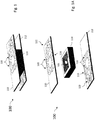
- Figure 1 is a diagram illustrating an optical atomic sensor 100 of one embodiment of the present disclosure.
- the optical atomic sensor comprises a first photonic integrated circuit 110 and a second photonic integrated circuit 112 aligned parallel to each other, and an atom trapping chamber 114 positioned between the first and second photonic integrated circuits 110, 112.
- Figure 1A is a partially exploded view of the optical atomic sensor 100 where the first photonic integrated circuit 110 is pulled away to reveal the inside of the atom trapping chamber 114.
- a portion of the lower surface first photonic integrated circuit 110 defines a first wall 116 exposed to the inside of the atom trapping chamber 114 while a portion of the upper surface of the second photonic integrated circuit 112 defines an opposing second wall 118 exposed to the inside of the atom trapping chamber 114.
- the atom trapping chamber 114 may be secured to first and second photonic integrated circuits 110, 112 by a bonding material.
- the atom trapping chamber 114 comprises an ultra-high vacuum chamber containing an atomic vapor.
- the atomic vapor is laser cooled by lasers emitted from the first and second photonic integrated circuits 110, 112 (as further discussed below) to form a sample of laser cooled atoms 105 at the center of the atom trapping chamber 114.
- the particular atoms 105 selected for loading into the chamber 114 would be based on the specific parameters the resulting sensor is intended to sense. This selection may be readily determined by one of ordinary skill in the art who has studied this disclosure.
- the atomic vapor may comprise atoms such as, but not limited to, cesium, strontium, ytterbium or rubidium, for example.
- any sample of atoms 105 that are known to those in the art as having cycling transition states and can be trapped and cooled by applying a combination of lasers and magnetic field may be utilized within the chamber 114.
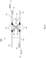
- the first and second photonic integrated circuits 110, 112 each comprise a plurality of grating emitters 120 that emit laser light into the atom trapping chamber 114, such as the example pattern of grating emitters 120 shown in Figure 2 .
- a first pattern of grating emitters 120 is arranged on a surface of the first photonic integrated circuits 110 that defines the first wall 116
- a coordinated second pattern of grating emitters 120 is arranged on the a surface of the second photonic integrated circuits 110 that defines the second wall 118 in order to launch laser light into the atom trapping chamber 114 from opposing directions.
- these grating emitters 120 on the first and second photonic integrated circuits 110, 112 deliver all the laser light needed to implement collecting, cooling, and trapping the atomic vapor to form a sample of laser cooled atoms 105 at the center of the atom trapping chamber 114, and for probing the states of the laser cooled atom sample in order to derive sensor measurements.
- the grating emitters 120 are lithographically patterned diffraction gratings fabricated into the surfaces of the first and second photonic integrated circuits 110, 112.
- the grating emitters 120 are lithographically patterned onto one or more thin film material layers on the first and second photonic integrated circuits 110, 112, such as a silicon nitride thin film layer.
- the grating emitters 120 may be arranged patterns on the first and second photonic integrated circuits 110, 112 so as to produce at least one atom trap inside the chamber 114, but may also be utilized to produce a plurality of overlapping atom traps of different types inside the chamber 114.
- Laser light is delivered to the grating emitters 120 via a system of waveguide circuits 122 fabricated within each of the first and second photonic integrated circuits 110, 112.
- the grating emitters 120 may each be considered as form of passive optical mode converter that converts light beams from a waveguide mode to free space travelling mode.
- the laser beams are directed from the waveguides 122 into free space by the grating emitters 120 with a defined direction, gaussian waist parameters, and polarization, for critical proper functioning of the sensor 100.
- these parameters being implemented using bulk optic, they are instead established by the lithographic patterns which make up the waveguides 122 and grating emitters 120. Thus, during mass-production they are highly reproducible from part to part.
- the one or more laser light sources 130 that generate the laser light carried by the waveguides 122 to the grating emitters 120 may be fabricated on-chip. That is, the laser light sources 130 may be laser devices fabricated into or onto the first and second photonic integrated circuits 110, 112 and directly feed laser light into the waveguides 122 that feed the grating emitters 120. In another embodiment, the laser light sources 130 may be off-chip laser devices (as shown at 135) and their laser light output is coupled into the waveguides 122 of the first and second photonic integrated circuits 110, 112.
- the particular wavelengths, and the number of different wavelengths, of laser light emitted into the chamber 114 will vary. As such the number of laser light sources 130 and the wavelengths they emit are selected accordingly.
- the laser light wavelengths generated by the laser sources 130 may match transition frequency characteristics of the particular atoms in the atom sample that need to be cooled.
- at least one laser light wavelength generated by the laser sources 130 may be adjustable to approximately match an energy gap of the atoms in the atom sample. It should be understood that the parameters of wavelength and frequency for laser light beams are by definition inversely proportional parameters for characterizing the color of that light beam.
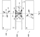
- Figure 4 is a diagram illustrating an example embodiment of sensor 100 generating one form of an atom trap 140 holding the atom sample 105.
- the grating emitters 120 are arranged in a coordinated pattern of three emitters on each of the first and second photonic integrated circuits 110, 112 as shown generally at 410 and 430.
- these two grating emitters 120 which may be referred to herein together as a set of “trapping emitter pairs” are arranged to aim the light they emit directly at each other and such that their respective laser light beams both pass through the center of the trapped cloud of atom vapor 105.
- the atom trap 140 is implemented using sets of the trapping emitter pairs arranged to produce mutually orthogonal laser light beams 138.
- the grating emitters 120 for the three sets of trapping emitter pairs may be arranged in a pattern such as a circle of uniform radius centered on the axis 440 which passes through the position of the trapped atom cloud along the edges of a hypothetical cube commonly referred to as the "[111]" configuration.
- a launch angle of 54.7 degrees would result in each of the six laser beams intersecting at the center of the trapped atomic sample in an orthogonal configuration.
- another form of atom trap 140 (such as traps referred to as an optical dipole, or optical dipole lattice trap) may be formed by a single set of trapping emitter pairs that are each fabricated to launch light beams into the chamber 114 at angles of 90 degrees with respect the plane of their respective photonic integrated circuits 110, 112.
- atom cooling and trapping within the chamber may be implemented using multiple laser beams of different wavelengths.
- the different wavelengths may be selected to align with different atomic transition levels of the atomic vapor, or for other reasons such as to produce multiple traps 140 within the chamber 114.
- the same grating emitters 120 may be utilized to emit light at each of the different wavelengths. By tailoring the parameters of the grating emitters 120, such as the period, spacing, and duty cycle of the patterned features that make up the grating emitters 120, laser beams with different wavelengths can be emitted at the same angle relative to the planes of their respective photonic integrated circuits 110, 112.
- the grating emitters 120 For example, by designing the grating emitters 120 to be fed by waveguides 122 from non-parallel directions on the photonic integrated circuits 110, 112, and by tailoring the shape of the patterned features that make up the grating emitters 120, two different wavelengths of laser light 138 can be made to emit from the same grating emitter 120 at the same angular direction.
- Such a grating emitter may be referred to as a "free space wavelength multiplexer grating emitter", which is an advancement over a single wavelength emitter, in that fewer emitters need be fabricated onto the photonic integrated circuits.
- the plurality of beams emitted by one emitter are overlapped and co-propagating, with no angle between them.
- Such a configuration is advantageous for some kinds of atom sensors such as clocks and gyroscopes.
- additional instances of set of trapping emitter pairs may be formed using additional grating emitters 120.
- multiple sets of three trapping emitter pairs of the type shown in Figure 4 may be used to project multiple instances of mutually orthogonal sets of laser light beams.
- cold atom sensors utilize two or more overlapping atom traps to function.
- a cold atom sensor 100 for operation as one particular type of laser cooled strontium optical lattice clock
- another type of atom trap 140 in which a so-called two stage magneto-optical-trap (“MOT") 140 is implemented.
- MOT magneto-optical-trap
- 12 laser beams 138 from 12 grating emitters 120 intersect at right angles at the atom sample 105 to produce two overlapping MOTS.
- these overlapping traps may be formed by laser beams with vastly different wavelengths (such as 461nm and 689nm, for example).
- the grating emitters 120 by arranging the grating emitters 120 in a pattern (such as the circle of uniform radius centered on the axis which passes through the position of the trapped atom cloud along the edges of the [111] cube configuration, for example) one or more MOTS can be made at the same position in the chamber 114.
- the emitted laser light beams 138 can be made to diverge, converge, or travel in a collimated fashion.
- 6 beams emitted from 6 grating emitters 120 e.g., arranged as two instances of three trapping emitter pairs
- 6 other beams may be of 2mm radius, but all 12 beams intersect in the same region.
- the photonic integrated circuits 110, 112 may comprise additional grating emitters 120 that can emit other beams at any desirable angle that does not interfere with the trapping laser beams (for example, not along the [111] angles) and can be located at other convenient places on the photonic integrated circuits 110, 112. Additional grating emitters 120 need not be arranged as emitter pairs, and may implement other functions such as launching repumping beams or probe beams which may be used for cold atom sensors.
- each grating emitter 120 may be fed with a waveguide or waveguides 122 carrying a potentially different wavelength or wavelengths from the other grating emitters 120.
- a waveguide or waveguides 122 carrying a potentially different wavelength or wavelengths from the other grating emitters 120.
- many large or small beams, of a variety of wavelengths and gaussian beam parameters, can all be directed and focused into the atom trapping chamber 114 and focused into the atom sample 105 without bulk mirrors or lenses. This makes pointing and focusing of the sensor 100 robust against shock, vibration, or thermal excursion which can cause bulk elements to move out of position.
- each of the emitted beams used for cooling and trapping are circularly polarized.
- This polarization can be achieved by tailoring the structures which make up the grating emitters 120 (and/or the waveguides 120 that feed those emitters 120) to produce linear, elliptical, or circular polarization, and can be done so for any emitted wavelength.
- the many beams used in the atom trap 140 can have tailored polarization without using bulk waveplates or retarders. This also makes the polarization robust against shock, vibration, or thermal excursions which can cause bulk elements to change their polarizing properties.
- the sensor 100 may be used to implement a third, different kind of trap, that is overlapped with one or more atom traps 140 within the atom tapping chamber 114.
- a third, different kind of trap that is overlapped with one or more atom traps 140 within the atom tapping chamber 114.
- One example of such an implementation would be for a strontium optical lattice clock.
- either a one-dimensional or three- dimensional optical dipole lattice trap 540 overlaps with a three orthogonal axis atom trap 140 (such as shown in Figure 4 ), within the atom tapping chamber 114.
- the optical dipole lattice trap 540 is produced by a grating emitter 120 (shown at 520 in Figure 5 ) that is structured to emit a laser light beam from the first photonic integrated circuit 110 into the chamber 114 to produce a beam 148 that exhibits a gaussian waist at the surface 118 of the second photonic integrated circuit 112 that is in a hemispherical resonator spatial optical mode with interference fringes in the three orthogonal axis atom trap 140.
- a grating emitter 120 shown at 520 in Figure 5
- the optical dipole lattice trap 540 is produced by a grating emitter 120 (shown at 520 in Figure 5 ) that is structured to emit a laser light beam from the first photonic integrated circuit 110 into the chamber 114 to produce a beam 148 that exhibits a gaussian waist at the surface 118 of the second photonic integrated circuit 112 that is in a hemispherical resonator spatial optical mode with interference fringes in the three
- the probe beam (which has a different wavelength of laser light than the beam(s) forming the optical dipole lattice trap 540) can be emitted from a grating emitter 120 that is located at the waist of the lattice (dipole) beam on the photonic integrated circuit 110.
- the grating emitter 120 may comprise an optical coating that reflects at the wavelength of the lattice (dipole) laser beam, but transmits at the wavelength of the probe beam such that the probe beam propagates along the axis of the lattice (dipole) trap, probing the trapped atoms.
- two laser light beams are emitted, one from a grating emitter 120 of the first photonic integrated circuit 110 (Shown at 620 in Figure 6 ) and one from a grating emitter 120 of the second photonic integrated circuit 112 (Shown at 622 in Figure 6 ).
- Each of these two grating emitters 620, 622 is structured to emit a laser light beam that beam exhibits a gaussian waist at the location of the three orthogonal axis atom trap 140, in a confocal resonator spatial optical mode with interference fringes in the three orthogonal axis atom trap 140.
- the two grating emitters 620, 622 may be considered to form a single set of trapping emitter pairs (such as previously described above) that are each fabricated to launch light beams into the chamber 114 at angles of 90 degrees (or other set of supplementary angles) with respect the plane of their respective photonic integrated circuits 110, 112.
- the three orthogonal axis atom trap 140 and optical dipole lattice trap 640 formed in this way overlap is guaranteed by virtue of the arrangement and design of the multiple grating emitters 120 on the photonic integrated circuits 110, 112. As such, this configuration allows the various traps to remain well aligned, so that the atomic sensor 100 performance is optimal.
- control of the light beams 138 emitted from the grating emitters 120 can be implemented in various ways.
- the sensor 100 may include, or otherwise be coupled to, a control circuit 750 to control various aspects of the light beams 138 entering the chamber 114.
- the control circuit 150 may control operation of one or more of the laser light sources 130 or 135 in order cycle the light output on and off, or control the wavelength of light generated by the laser light sources 140.
- the controller 750 may further operated optical control elements such as shutters 752 or modulators 754 (which in some embodiments may be fabricated into or on to the photonic integrated circuits 110, 112). By controlling of the laser light beams entering the chamber 114, the controller 750 may cycle the trapped atoms through atomic transitions and cycle the sensor 100 between trapping and probing states. In some embodiments, the controller 750 may cycle the laser light beams so that beams of different wavelengths are emitted into the chamber 114 at different times.
- optical control elements such as shutters 752 or modulators 754 (which in some embodiments may be fabricated into or on to the photonic integrated circuits 110, 112).
- the senor 100 cycles between trapping and probing modes under control of the controller 750. It is during probing that characteristics of the atomic sample are measured by emitting a laser light beam from a grating emitter 120.
- the sensor 100 may further comprise at least one optical detector 760 (which in some embodiments may be fabricated into or on to the photonic integrated circuits 110, 112) to capture measurements or images from within the chamber 114. The output of the optical detector 760 may then be provided back to the controller 750 or other device for processing.
- the frequency of the laser light beam used for probing is adjusted by the controller 750 to match the corresponding energy gap of the atoms that make up the atom cloud 105.
- the energy gap has an invariant frequency associated with it that is proportion to the energy of the gap of the atoms.
- the laser beam is directed by a grating emitter 120 through the atom cloud 105 and measured on the other side (for example, by optical detector 760) and used to servo control the light source 130,135 producing the laser beam.
- the frequency of the laser light When the frequency of the laser light is adjusted so that it matches the frequency of the atoms' energy gap, a minimum in the amount of light passing thought the cloud 105 will be observed due to absorption of a percentage of the light by the atom cloud.
- the frequency of the laser light may then be used for the purpose of accurately measuring time.
- the operation of the sensor 100 is substantially similar.
- the difference would be what characteristic or state of the atom cloud 105 is measured by the probing laser beam while the trapping laser beams are cycled off.
- the atoms will shift in position as they "fall” or become displaced within the chamber 114 due to linear acceleration of the sensor 100.
- the probing laser beam passes through the atom cloud 105 and detector 760 reads an atomic fringe or interferometric pattern to characterize motion of the atoms based on their quantum properties.
- the atoms of atom cloud 105 are typically alkali atoms for such an embodiment and may comprise rubidium or cesium atoms.
- the laser cooling cools the atoms of cloud 105 down to a temperature of approximately 1 micro-Kelvin. Once cooled, the cold atom cloud 105 is released into an optical lattice and subjected to optical pulses from the grating emitters 120 to form an inertial sensor. After the atom cloud 105 is cooled, interfering laser beams of offsetting frequency are applied into the chamber 114.
- the optical lattice creates an energy/potential well for the atoms.
- the lattice By slightly detuning the relative frequency difference of the two interfering laser beams to form that optical lattice, the lattice to begins to move and the atoms trapped in various antinodes of the lattice potential will begin to accelerate with it.
- a plane is selected in which to create the interferometer split wave-function paths, and that plane will be perpendicular to the rotation axis along which rotation sensing is desired.
- the structure of sensor 100 contributed to efficiencies in device fabrication.
- alignment of the photonic integrated circuits 110, 112 may be achieved by emitting light beams from grating emitters 120 on one of the photonic integrated circuits and measuring the power of light beam received at corresponding grating emitters 120 on the other of the photonic integrated circuits.
- the photonic integrated circuit 110 may be held by a pick-and-place positioner while the photonic integrated circuit 120 is held in a manifold of an optical detector.
- the two photonic integrated circuits 110, 112 are aligned and may be cemented in place to the walls of the chamber 114.
- the two photonic integrated circuits 110, 112 are registered relative to one another in an alignment procedure.
- the photonic integrated circuits 110, 112 are situated on either side of the chamber 114. Alignment of the two photonic integrated circuits 110, 112 is achieved by maximizing the coupling of light from the grating emitter 120 on photonic integrated circuits 110 into the grating emitters 120 photonic integrated circuits 112 (which are now acting as "receivers").
- the amount light coupled from the one emitter emitting light into its paired emitter on the other photonic integrated circuits receiving light can be maximized.
- cross coupled power may be maximized both ways. In this way the alignment can be done with real time feedback during manufacture.
- the photonic integrated circuits 110, 112 are permanently bonded to the opposing sides of the chamber 114 (for example, via optical contacting to the glass walls of the vacuum cell, or to a hollow spacer into which the vacuum cell can be inserted).
- the region of beam overlap of the MOT beams emitted from both photonic integrated circuit 110, 112 is thus defined with no need for adjustable bulk optics. This results in an optical atomic sensor 100 in which the optics system can be first optimized for performance, then locked down to make the sensor robust.
Landscapes
- Physics & Mathematics (AREA)
- General Physics & Mathematics (AREA)
- Optics & Photonics (AREA)
- Engineering & Computer Science (AREA)
- Radar, Positioning & Navigation (AREA)
- Remote Sensing (AREA)
- Electromagnetism (AREA)
- Power Engineering (AREA)
- Condensed Matter Physics & Semiconductors (AREA)
- Investigating Or Analysing Materials By Optical Means (AREA)
- Lasers (AREA)
Claims (10)
- Capteur atomique optique (100), le capteur (100) comprenant :un premier circuit intégré photonique (110) ;un second circuit intégré photonique (112) ; etune chambre de piégeage d'atomes (114) positionnée entre et liée au premier circuit intégré photonique (110) et second circuit intégré photonique (112), le premier circuit intégré photonique (110) et le second circuit intégré photonique (112) étant alignés parallèlement l'un à l'autre ; etun échantillon de vapeur atomique (105) enfermé à l'intérieur de la chambre de piégeage d'atomes (114) ;dans lequel le premier circuit intégré photonique (110) et le second circuit intégré photonique (112) comprennent chacun :une pluralité d'émetteurs de réseau (120) fabriqués dans des surfaces respectives des premier et second circuits intégrés photoniques (112) ;un système de guides d'ondes (122) conçu pour coupler la lumière laser d'une ou plusieurs sources de lumière laser à la pluralité d'émetteurs de réseau (120) ;dans lequel au moins l'un de la pluralité d'émetteurs de réseau (120) de chacun du premier circuit intégré photonique (110) et du second circuit intégré photonique (112) est agencé pour lancer des faisceaux de lumière laser (138) dans la chambre de piégeage d'atomes (114) selon un motif structuré pour refroidir la vapeur atomique (105) et pour produire au moins un piège à atomes (140) à l'intérieur de la chambre de piégeage d'atomes (114) ; etdans lequel la pluralité d'émetteurs de réseau (120) comporte en outre au moins un émetteur de réseau (120) conçu pour émettre une sonde de lumière laser dans la vapeur atomique (105).
- Capteur (100) selon la revendication 1, dans lequel les faisceaux de lumière laser (138) sont dirigés depuis le système de guides d'ondes (122) vers l'espace libre à l'intérieur de la chambre de piégeage d'atomes (114) à un angle défini par une structure des émetteurs de réseau (120).
- Capteur (100) selon la revendication 2, dans lequel l'un ou les deux parmi le système de guides d'ondes (122) et les émetteurs de réseau (120) sont conçus pour régler soit les paramètres de taille gaussienne, soit la polarisation des faisceaux de lumière laser (138).
- Système selon la revendication 1, dans lequel la vapeur atomique (105) comprend des atomes ayant des états de transition cycliques et caractérisés par le fait qu'ils peuvent être refroidis et piégés à l'aide de la lumière laser.
- Capteur (100) selon la revendication 1, dans lequel pour chacun de la pluralité d'émetteurs de réseau (120) sur le premier circuit intégré photonique (110), il y a un émetteur de réseau complémentaire (120) de la pluralité d'émetteurs de réseau (120) sur le second circuit intégré photonique (112) définissant un ensemble de paires d'émetteurs de piégeage, l'ensemble de paires d'émetteurs de piégeage étant agencé pour diriger les faisceaux de lumière laser respectifs (138) qu'ils émettent directement l'un sur l'autre et de telle sorte que leurs faisceaux de lumière laser respectifs (138) passent par le centre de l'au moins un piège à atomes (140).
- Capteur (100) selon la revendication 1, dans lequel l'au moins un piège à atomes (140) à l'intérieur de la chambre comprend soit un piège à atomes (140) à trois axes orthogonaux, un piège à réseau dipolaire optique, ou une combinaison d'un piège à atomes (140) à trois axes orthogonaux et d'un piège à réseau dipolaire optique.
- Capteur (100) selon la revendication 6, dans lequel le piège à réseau dipolaire optique est généré par un premier émetteur de réseau (120) structuré pour émettre un faisceau de lumière laser depuis le premier circuit intégré photonique (110) vers la chambre de piégeage d'atomes (114) de sorte que le faisceau de lumière laser présente une taille gaussienne à une surface du second circuit intégré photonique (112), dans un mode optique spatial à résonateur hémisphérique avec des franges d'interférence dans l'au moins un piège à atomes (140) formé à l'intérieur de la chambre de piégeage d'atomes (114).
- Capteur (100) selon la revendication 6, dans lequel le piège à réseau dipolaire optique est généré par un premier émetteur de réseau (120) sur le premier circuit intégré photonique (110) et un second émetteur de réseau (120) à partir du second circuit intégré photonique (112), dans lequel chacun des premier et second émetteurs de réseau (120) est structuré pour émettre un faisceau de lumière laser dont le faisceau présente une taille gaussienne à un emplacement de l'au moins un piège à atomes (140) également formé dans la chambre de piégeage des atomes (114), dans un mode optique spatial de résonateur confocal avec des franges d'interférence dans l'au moins un piège à atomes (140).
- Capteur (100) selon la revendication 1, dans lequel un premier ensemble de la pluralité d'émetteurs de réseau (120) transmet des faisceaux de lumière laser (138) d'une première longueur d'onde, et un second ensemble de la pluralité d'émetteurs de réseau (120) émet des faisceaux de lumière laser (138) d'une seconde longueur d'onde, la première longueur d'onde étant différente de la seconde longueur d'onde ;
dans lequel le premier ensemble de la pluralité d'émetteurs de réseau (120) et le second ensemble de la pluralité d'émetteurs de réseau (120) sont structurés pour projeter les faisceaux de lumière laser (138) de la première longueur d'onde et les faisceaux de lumière laser (138) de la seconde longueur d'onde afin qu'ils se croisent au centre de l'au moins un piège à atomes (140) à l'intérieur de la chambre. - Capteur (100) selon la revendication 1, dans lequel pour un premier ensemble de la pluralité d'émetteurs de réseau (120), chacun des émetteurs de réseau (120) reçoit une lumière laser d'une première longueur d'onde du système de guides d'ondes (122) et une lumière laser d'une seconde longueur d'onde du système de guides d'ondes (122), la première longueur d'onde étant différente de la seconde longueur d'onde ;
dans lequel chacun dudit premier ensemble de la pluralité d'émetteurs de réseau (120) est structuré pour projeter les faisceaux de lumière laser (138) de la première longueur d'onde et les faisceaux de lumière laser (138) de la seconde longueur d'onde pour qu'ils se croisent en un centre de l'au moins un piège à atomes (140) à l'intérieur de la chambre.
Applications Claiming Priority (1)
| Application Number | Priority Date | Filing Date | Title |
|---|---|---|---|
| US16/431,360 US11402241B2 (en) | 2019-06-04 | 2019-06-04 | Systems and methods for an integrated optical atomic sensor |
Publications (2)
| Publication Number | Publication Date |
|---|---|
| EP3748295A1 EP3748295A1 (fr) | 2020-12-09 |
| EP3748295B1 true EP3748295B1 (fr) | 2021-09-22 |
Family
ID=70921732
Family Applications (1)
| Application Number | Title | Priority Date | Filing Date |
|---|---|---|---|
| EP20177276.1A Active EP3748295B1 (fr) | 2019-06-04 | 2020-05-28 | Systèmes et procédés pour un capteur atomique optique intégré |
Country Status (3)
| Country | Link |
|---|---|
| US (1) | US11402241B2 (fr) |
| EP (1) | EP3748295B1 (fr) |
| CN (1) | CN112034696B (fr) |
Families Citing this family (10)
| Publication number | Priority date | Publication date | Assignee | Title |
|---|---|---|---|---|
| US11402241B2 (en) * | 2019-06-04 | 2022-08-02 | Honeywell International Inc. | Systems and methods for an integrated optical atomic sensor |
| WO2021005235A1 (fr) * | 2019-07-10 | 2021-01-14 | Rockley Photonics Limited | Structure de trou d'interconnexion de moule |
| EP4091005B1 (fr) * | 2020-01-16 | 2026-01-28 | SRI International | Ensembles de cellules sous vide intégrées |
| EP4120905A4 (fr) * | 2020-03-19 | 2024-04-03 | SRI International | Capteur de champ électromagnétique quantique et imageur |
| US12046387B2 (en) * | 2020-09-16 | 2024-07-23 | ColdQuanta, Inc. | Vacuum cell with integrated guide stack wall |
| CN112729355B (zh) * | 2020-12-24 | 2023-03-17 | 华中光电技术研究所(中国船舶重工集团公司第七一七研究所) | 一种适用于原子干涉仪的标定拉曼光入射角度的方法 |
| CN112864790B (zh) * | 2021-01-26 | 2021-12-28 | 北京大学 | 一种10mHz极窄线宽激光器及其实现方法 |
| US12411263B2 (en) * | 2021-09-08 | 2025-09-09 | ColdQuanta, Inc. | Ultra-high-vacuum cell with integrated meta-optics |
| US20230232561A1 (en) * | 2021-12-21 | 2023-07-20 | ColdQuanta, Inc. | Method and system for providing multiple seals for a compact vacuum cell |
| CN115988727A (zh) * | 2022-12-01 | 2023-04-18 | 华中光电技术研究所(中国船舶集团有限公司第七一七研究所) | 一种光集成一体式原子芯片及其制作方法 |
Family Cites Families (12)
| Publication number | Priority date | Publication date | Assignee | Title |
|---|---|---|---|---|
| US7102451B2 (en) | 2004-02-18 | 2006-09-05 | Princeton University, Office Of Technology, Licensing & Intellectual Property | Method and system for operating an atomic clock with alternating-polarization light |
| US8829423B2 (en) | 2012-07-12 | 2014-09-09 | Honeywell International Inc. | Folded optics for batch fabricated atomic sensor |
| US9410885B2 (en) | 2013-07-22 | 2016-08-09 | Honeywell International Inc. | Atomic sensor physics package having optically transparent panes and external wedges |
| US9778328B2 (en) * | 2014-05-30 | 2017-10-03 | Northrop Grumman Systems Corporation | Optical probe beam stabilization in an atomic sensor system |
| EP3170052B1 (fr) * | 2014-07-17 | 2023-04-26 | CSEM Centre Suisse D'electronique Et De Microtechnique SA | Horloge atomique |
| US9175960B1 (en) * | 2014-09-10 | 2015-11-03 | Honeywell International Inc. | Optically dithered atomic gyro-compass |
| FR3044398B1 (fr) * | 2015-11-27 | 2019-07-19 | Thales | Source laser pour capteur inertiel a atomes froids |
| US10278275B2 (en) * | 2016-02-12 | 2019-04-30 | Utah State University Research Foundation | Grating magneto optical trap |
| US9989926B2 (en) * | 2016-02-19 | 2018-06-05 | Honeywell International Inc. | Systems and methods for positionally stable magneto-optical trapping over temperature |
| US10352702B2 (en) | 2016-09-02 | 2019-07-16 | Honeywell International Inc. | Fully reciprocal atomic interferometric gyroscope |
| US11291103B2 (en) * | 2018-10-11 | 2022-03-29 | Government Of The United States Of America, As Represented By The Secretary Of Commerce | Uniaxial counter-propagating monolaser atom trap |
| US11402241B2 (en) * | 2019-06-04 | 2022-08-02 | Honeywell International Inc. | Systems and methods for an integrated optical atomic sensor |
-
2019
- 2019-06-04 US US16/431,360 patent/US11402241B2/en active Active
-
2020
- 2020-05-28 EP EP20177276.1A patent/EP3748295B1/fr active Active
- 2020-06-04 CN CN202010502888.4A patent/CN112034696B/zh active Active
Also Published As
| Publication number | Publication date |
|---|---|
| CN112034696A (zh) | 2020-12-04 |
| US20200386581A1 (en) | 2020-12-10 |
| EP3748295A1 (fr) | 2020-12-09 |
| US11402241B2 (en) | 2022-08-02 |
| CN112034696B (zh) | 2024-04-30 |
Similar Documents
| Publication | Publication Date | Title |
|---|---|---|
| EP3748295B1 (fr) | Systèmes et procédés pour un capteur atomique optique intégré | |
| JP7216110B2 (ja) | 静止面および回転面上において横揺れ角を測定するための光学分度器 | |
| US8373112B2 (en) | Cold atom interferometry sensor | |
| US9134450B2 (en) | Cold atom gravity gradiometer | |
| CN111561920B (zh) | 圆形谐振器倏逝波捕集的原子陀螺仪 | |
| KR20130100693A (ko) | 조명 광학계, 분광 측정용 광조사 장치 및 분광 측정 장치 | |
| US20240203616A1 (en) | Photonic Integrated Beamlines for 3D Magneto-Optical Trap | |
| CN114441794B (zh) | 基于固态原子自旋几何相的光悬浮角速度测量装置与方法 | |
| CN110231088B (zh) | 基于量子弱测量的oam光束重心位移测量装置及方法 | |
| JP6285808B2 (ja) | 干渉計 | |
| KR101028061B1 (ko) | 결맞은 광섬유 테이퍼를 이용한 간섭무늬 안정화된 간섭계 | |
| EP4409226A1 (fr) | Filtrage d'espace de phase dans des capteurs inertiels à faisceaux thermiques | |
| EP4481326A1 (fr) | Capteurs atomiques à base de puce photonique | |
| US20240412888A1 (en) | Photonically integrated atomic tweezer clock | |
| Lee et al. | A cold-atom interferometer with microfabricated gratings and a single seed laser | |
| CA2807120C (fr) | Dispositif de resonance optique a trois dimensions, procede d'oscillation laser polarisee, et systeme d'oscillation laser polarisee | |
| US12424810B1 (en) | Compact atom interferometry inertial navigation sensors with tailored diffractive optics | |
| CN118633214A (zh) | 磁光阱装置、物理封装、光晶格钟用物理封装、原子钟用物理封装、原子干涉仪用物理封装、量子信息处理设备用物理封装以及物理封装系统 | |
| Morris | Development Of A Prototype Atomic Interferometer For Fundamental Physics Searches. | |
| US20250208162A1 (en) | Quantum inertial measurement unit and method for acquiring at least one physical measured quantity | |
| JP2010520994A (ja) | 光学計測システム | |
| US12449256B1 (en) | Compact grating magneto-optical trap sensor head for inertial navigation in dynamic environments | |
| Heffer | Towards precision gravimetry using light-pulse atom interferometry | |
| JP2009294165A (ja) | 周回光路装置及び3軸リングレーザジャイロ | |
| Benito | Optical cavity integrated surface ion trap for enhanced light collection |
Legal Events
| Date | Code | Title | Description |
|---|---|---|---|
| PUAI | Public reference made under article 153(3) epc to a published international application that has entered the european phase |
Free format text: ORIGINAL CODE: 0009012 |
|
| STAA | Information on the status of an ep patent application or granted ep patent |
Free format text: STATUS: THE APPLICATION HAS BEEN PUBLISHED |
|
| AK | Designated contracting states |
Kind code of ref document: A1 Designated state(s): AL AT BE BG CH CY CZ DE DK EE ES FI FR GB GR HR HU IE IS IT LI LT LU LV MC MK MT NL NO PL PT RO RS SE SI SK SM TR |
|
| AX | Request for extension of the european patent |
Extension state: BA ME |
|
| STAA | Information on the status of an ep patent application or granted ep patent |
Free format text: STATUS: REQUEST FOR EXAMINATION WAS MADE |
|
| 17P | Request for examination filed |
Effective date: 20210104 |
|
| RBV | Designated contracting states (corrected) |
Designated state(s): AL AT BE BG CH CY CZ DE DK EE ES FI FR GB GR HR HU IE IS IT LI LT LU LV MC MK MT NL NO PL PT RO RS SE SI SK SM TR |
|
| GRAP | Despatch of communication of intention to grant a patent |
Free format text: ORIGINAL CODE: EPIDOSNIGR1 |
|
| STAA | Information on the status of an ep patent application or granted ep patent |
Free format text: STATUS: GRANT OF PATENT IS INTENDED |
|
| INTG | Intention to grant announced |
Effective date: 20210413 |
|
| GRAS | Grant fee paid |
Free format text: ORIGINAL CODE: EPIDOSNIGR3 |
|
| GRAA | (expected) grant |
Free format text: ORIGINAL CODE: 0009210 |
|
| STAA | Information on the status of an ep patent application or granted ep patent |
Free format text: STATUS: THE PATENT HAS BEEN GRANTED |
|
| AK | Designated contracting states |
Kind code of ref document: B1 Designated state(s): AL AT BE BG CH CY CZ DE DK EE ES FI FR GB GR HR HU IE IS IT LI LT LU LV MC MK MT NL NO PL PT RO RS SE SI SK SM TR |
|
| REG | Reference to a national code |
Ref country code: GB Ref legal event code: FG4D |
|
| REG | Reference to a national code |
Ref country code: IE Ref legal event code: FG4D |
|
| REG | Reference to a national code |
Ref country code: DE Ref legal event code: R096 Ref document number: 602020000593 Country of ref document: DE |
|
| REG | Reference to a national code |
Ref country code: CH Ref legal event code: EP Ref country code: AT Ref legal event code: REF Ref document number: 1432664 Country of ref document: AT Kind code of ref document: T Effective date: 20211015 |
|
| REG | Reference to a national code |
Ref country code: LT Ref legal event code: MG9D |
|
| REG | Reference to a national code |
Ref country code: NL Ref legal event code: MP Effective date: 20210922 |
|
| PG25 | Lapsed in a contracting state [announced via postgrant information from national office to epo] |
Ref country code: SE Free format text: LAPSE BECAUSE OF FAILURE TO SUBMIT A TRANSLATION OF THE DESCRIPTION OR TO PAY THE FEE WITHIN THE PRESCRIBED TIME-LIMIT Effective date: 20210922 Ref country code: RS Free format text: LAPSE BECAUSE OF FAILURE TO SUBMIT A TRANSLATION OF THE DESCRIPTION OR TO PAY THE FEE WITHIN THE PRESCRIBED TIME-LIMIT Effective date: 20210922 Ref country code: HR Free format text: LAPSE BECAUSE OF FAILURE TO SUBMIT A TRANSLATION OF THE DESCRIPTION OR TO PAY THE FEE WITHIN THE PRESCRIBED TIME-LIMIT Effective date: 20210922 Ref country code: FI Free format text: LAPSE BECAUSE OF FAILURE TO SUBMIT A TRANSLATION OF THE DESCRIPTION OR TO PAY THE FEE WITHIN THE PRESCRIBED TIME-LIMIT Effective date: 20210922 Ref country code: NO Free format text: LAPSE BECAUSE OF FAILURE TO SUBMIT A TRANSLATION OF THE DESCRIPTION OR TO PAY THE FEE WITHIN THE PRESCRIBED TIME-LIMIT Effective date: 20211222 Ref country code: BG Free format text: LAPSE BECAUSE OF FAILURE TO SUBMIT A TRANSLATION OF THE DESCRIPTION OR TO PAY THE FEE WITHIN THE PRESCRIBED TIME-LIMIT Effective date: 20211222 Ref country code: LT Free format text: LAPSE BECAUSE OF FAILURE TO SUBMIT A TRANSLATION OF THE DESCRIPTION OR TO PAY THE FEE WITHIN THE PRESCRIBED TIME-LIMIT Effective date: 20210922 |
|
| REG | Reference to a national code |
Ref country code: AT Ref legal event code: MK05 Ref document number: 1432664 Country of ref document: AT Kind code of ref document: T Effective date: 20210922 |
|
| PG25 | Lapsed in a contracting state [announced via postgrant information from national office to epo] |
Ref country code: LV Free format text: LAPSE BECAUSE OF FAILURE TO SUBMIT A TRANSLATION OF THE DESCRIPTION OR TO PAY THE FEE WITHIN THE PRESCRIBED TIME-LIMIT Effective date: 20210922 Ref country code: GR Free format text: LAPSE BECAUSE OF FAILURE TO SUBMIT A TRANSLATION OF THE DESCRIPTION OR TO PAY THE FEE WITHIN THE PRESCRIBED TIME-LIMIT Effective date: 20211223 |
|
| PG25 | Lapsed in a contracting state [announced via postgrant information from national office to epo] |
Ref country code: AT Free format text: LAPSE BECAUSE OF FAILURE TO SUBMIT A TRANSLATION OF THE DESCRIPTION OR TO PAY THE FEE WITHIN THE PRESCRIBED TIME-LIMIT Effective date: 20210922 |
|
| PG25 | Lapsed in a contracting state [announced via postgrant information from national office to epo] |
Ref country code: IS Free format text: LAPSE BECAUSE OF FAILURE TO SUBMIT A TRANSLATION OF THE DESCRIPTION OR TO PAY THE FEE WITHIN THE PRESCRIBED TIME-LIMIT Effective date: 20220122 Ref country code: SK Free format text: LAPSE BECAUSE OF FAILURE TO SUBMIT A TRANSLATION OF THE DESCRIPTION OR TO PAY THE FEE WITHIN THE PRESCRIBED TIME-LIMIT Effective date: 20210922 Ref country code: RO Free format text: LAPSE BECAUSE OF FAILURE TO SUBMIT A TRANSLATION OF THE DESCRIPTION OR TO PAY THE FEE WITHIN THE PRESCRIBED TIME-LIMIT Effective date: 20210922 Ref country code: PT Free format text: LAPSE BECAUSE OF FAILURE TO SUBMIT A TRANSLATION OF THE DESCRIPTION OR TO PAY THE FEE WITHIN THE PRESCRIBED TIME-LIMIT Effective date: 20220124 Ref country code: PL Free format text: LAPSE BECAUSE OF FAILURE TO SUBMIT A TRANSLATION OF THE DESCRIPTION OR TO PAY THE FEE WITHIN THE PRESCRIBED TIME-LIMIT Effective date: 20210922 Ref country code: NL Free format text: LAPSE BECAUSE OF FAILURE TO SUBMIT A TRANSLATION OF THE DESCRIPTION OR TO PAY THE FEE WITHIN THE PRESCRIBED TIME-LIMIT Effective date: 20210922 Ref country code: ES Free format text: LAPSE BECAUSE OF FAILURE TO SUBMIT A TRANSLATION OF THE DESCRIPTION OR TO PAY THE FEE WITHIN THE PRESCRIBED TIME-LIMIT Effective date: 20210922 Ref country code: EE Free format text: LAPSE BECAUSE OF FAILURE TO SUBMIT A TRANSLATION OF THE DESCRIPTION OR TO PAY THE FEE WITHIN THE PRESCRIBED TIME-LIMIT Effective date: 20210922 Ref country code: CZ Free format text: LAPSE BECAUSE OF FAILURE TO SUBMIT A TRANSLATION OF THE DESCRIPTION OR TO PAY THE FEE WITHIN THE PRESCRIBED TIME-LIMIT Effective date: 20210922 Ref country code: AL Free format text: LAPSE BECAUSE OF FAILURE TO SUBMIT A TRANSLATION OF THE DESCRIPTION OR TO PAY THE FEE WITHIN THE PRESCRIBED TIME-LIMIT Effective date: 20210922 |
|
| REG | Reference to a national code |
Ref country code: DE Ref legal event code: R097 Ref document number: 602020000593 Country of ref document: DE |
|
| PG25 | Lapsed in a contracting state [announced via postgrant information from national office to epo] |
Ref country code: DK Free format text: LAPSE BECAUSE OF FAILURE TO SUBMIT A TRANSLATION OF THE DESCRIPTION OR TO PAY THE FEE WITHIN THE PRESCRIBED TIME-LIMIT Effective date: 20210922 |
|
| PLBE | No opposition filed within time limit |
Free format text: ORIGINAL CODE: 0009261 |
|
| STAA | Information on the status of an ep patent application or granted ep patent |
Free format text: STATUS: NO OPPOSITION FILED WITHIN TIME LIMIT |
|
| 26N | No opposition filed |
Effective date: 20220623 |
|
| PG25 | Lapsed in a contracting state [announced via postgrant information from national office to epo] |
Ref country code: SI Free format text: LAPSE BECAUSE OF FAILURE TO SUBMIT A TRANSLATION OF THE DESCRIPTION OR TO PAY THE FEE WITHIN THE PRESCRIBED TIME-LIMIT Effective date: 20210922 |
|
| REG | Reference to a national code |
Ref country code: DE Ref legal event code: R119 Ref document number: 602020000593 Country of ref document: DE |
|
| REG | Reference to a national code |
Ref country code: BE Ref legal event code: MM Effective date: 20220531 |
|
| PG25 | Lapsed in a contracting state [announced via postgrant information from national office to epo] |
Ref country code: MC Free format text: LAPSE BECAUSE OF FAILURE TO SUBMIT A TRANSLATION OF THE DESCRIPTION OR TO PAY THE FEE WITHIN THE PRESCRIBED TIME-LIMIT Effective date: 20210922 Ref country code: LU Free format text: LAPSE BECAUSE OF NON-PAYMENT OF DUE FEES Effective date: 20220528 Ref country code: IT Free format text: LAPSE BECAUSE OF FAILURE TO SUBMIT A TRANSLATION OF THE DESCRIPTION OR TO PAY THE FEE WITHIN THE PRESCRIBED TIME-LIMIT Effective date: 20210922 |
|
| PG25 | Lapsed in a contracting state [announced via postgrant information from national office to epo] |
Ref country code: IE Free format text: LAPSE BECAUSE OF NON-PAYMENT OF DUE FEES Effective date: 20220528 |
|
| PG25 | Lapsed in a contracting state [announced via postgrant information from national office to epo] |
Ref country code: DE Free format text: LAPSE BECAUSE OF NON-PAYMENT OF DUE FEES Effective date: 20221201 Ref country code: BE Free format text: LAPSE BECAUSE OF NON-PAYMENT OF DUE FEES Effective date: 20220531 |
|
| P01 | Opt-out of the competence of the unified patent court (upc) registered |
Effective date: 20230526 |
|
| REG | Reference to a national code |
Ref country code: CH Ref legal event code: PL |
|
| PG25 | Lapsed in a contracting state [announced via postgrant information from national office to epo] |
Ref country code: LI Free format text: LAPSE BECAUSE OF NON-PAYMENT OF DUE FEES Effective date: 20230531 Ref country code: CH Free format text: LAPSE BECAUSE OF NON-PAYMENT OF DUE FEES Effective date: 20230531 |
|
| PG25 | Lapsed in a contracting state [announced via postgrant information from national office to epo] |
Ref country code: SM Free format text: LAPSE BECAUSE OF FAILURE TO SUBMIT A TRANSLATION OF THE DESCRIPTION OR TO PAY THE FEE WITHIN THE PRESCRIBED TIME-LIMIT Effective date: 20210922 Ref country code: MK Free format text: LAPSE BECAUSE OF FAILURE TO SUBMIT A TRANSLATION OF THE DESCRIPTION OR TO PAY THE FEE WITHIN THE PRESCRIBED TIME-LIMIT Effective date: 20210922 Ref country code: CY Free format text: LAPSE BECAUSE OF FAILURE TO SUBMIT A TRANSLATION OF THE DESCRIPTION OR TO PAY THE FEE WITHIN THE PRESCRIBED TIME-LIMIT Effective date: 20210922 |
|
| PG25 | Lapsed in a contracting state [announced via postgrant information from national office to epo] |
Ref country code: HU Free format text: LAPSE BECAUSE OF FAILURE TO SUBMIT A TRANSLATION OF THE DESCRIPTION OR TO PAY THE FEE WITHIN THE PRESCRIBED TIME-LIMIT; INVALID AB INITIO Effective date: 20200528 |
|
| PG25 | Lapsed in a contracting state [announced via postgrant information from national office to epo] |
Ref country code: MT Free format text: LAPSE BECAUSE OF FAILURE TO SUBMIT A TRANSLATION OF THE DESCRIPTION OR TO PAY THE FEE WITHIN THE PRESCRIBED TIME-LIMIT Effective date: 20210922 |
|
| GBPC | Gb: european patent ceased through non-payment of renewal fee |
Effective date: 20240528 |
|
| PG25 | Lapsed in a contracting state [announced via postgrant information from national office to epo] |
Ref country code: GB Free format text: LAPSE BECAUSE OF NON-PAYMENT OF DUE FEES Effective date: 20240528 |
|
| PGFP | Annual fee paid to national office [announced via postgrant information from national office to epo] |
Ref country code: FR Payment date: 20250526 Year of fee payment: 6 |
|
| PG25 | Lapsed in a contracting state [announced via postgrant information from national office to epo] |
Ref country code: TR Free format text: LAPSE BECAUSE OF FAILURE TO SUBMIT A TRANSLATION OF THE DESCRIPTION OR TO PAY THE FEE WITHIN THE PRESCRIBED TIME-LIMIT Effective date: 20210922 |