EP3748618A1 - Procédé de détection pour circuit de pixel, procédé d'excitation pour écran d'affichage et dispositif d'affichage - Google Patents
Procédé de détection pour circuit de pixel, procédé d'excitation pour écran d'affichage et dispositif d'affichage Download PDFInfo
- Publication number
- EP3748618A1 EP3748618A1 EP18882298.5A EP18882298A EP3748618A1 EP 3748618 A1 EP3748618 A1 EP 3748618A1 EP 18882298 A EP18882298 A EP 18882298A EP 3748618 A1 EP3748618 A1 EP 3748618A1
- Authority
- EP
- European Patent Office
- Prior art keywords
- voltage
- driving transistor
- data voltage
- sensing
- sensing voltage
- Prior art date
- Legal status (The legal status is an assumption and is not a legal conclusion. Google has not performed a legal analysis and makes no representation as to the accuracy of the status listed.)
- Withdrawn
Links
Images






Classifications
-
- G—PHYSICS
- G09—EDUCATION; CRYPTOGRAPHY; DISPLAY; ADVERTISING; SEALS
- G09G—ARRANGEMENTS OR CIRCUITS FOR CONTROL OF INDICATING DEVICES USING STATIC MEANS TO PRESENT VARIABLE INFORMATION
- G09G3/00—Control arrangements or circuits, of interest only in connection with visual indicators other than cathode-ray tubes
-
- G—PHYSICS
- G09—EDUCATION; CRYPTOGRAPHY; DISPLAY; ADVERTISING; SEALS
- G09G—ARRANGEMENTS OR CIRCUITS FOR CONTROL OF INDICATING DEVICES USING STATIC MEANS TO PRESENT VARIABLE INFORMATION
- G09G3/00—Control arrangements or circuits, of interest only in connection with visual indicators other than cathode-ray tubes
- G09G3/006—Electronic inspection or testing of displays and display drivers, e.g. of LED or LCD displays
-
- G—PHYSICS
- G09—EDUCATION; CRYPTOGRAPHY; DISPLAY; ADVERTISING; SEALS
- G09G—ARRANGEMENTS OR CIRCUITS FOR CONTROL OF INDICATING DEVICES USING STATIC MEANS TO PRESENT VARIABLE INFORMATION
- G09G3/00—Control arrangements or circuits, of interest only in connection with visual indicators other than cathode-ray tubes
- G09G3/20—Control arrangements or circuits, of interest only in connection with visual indicators other than cathode-ray tubes for presentation of an assembly of a number of characters, e.g. a page, by composing the assembly by combination of individual elements arranged in a matrix no fixed position being assigned to or needed to be assigned to the individual characters or partial characters
- G09G3/22—Control arrangements or circuits, of interest only in connection with visual indicators other than cathode-ray tubes for presentation of an assembly of a number of characters, e.g. a page, by composing the assembly by combination of individual elements arranged in a matrix no fixed position being assigned to or needed to be assigned to the individual characters or partial characters using controlled light sources
- G09G3/30—Control arrangements or circuits, of interest only in connection with visual indicators other than cathode-ray tubes for presentation of an assembly of a number of characters, e.g. a page, by composing the assembly by combination of individual elements arranged in a matrix no fixed position being assigned to or needed to be assigned to the individual characters or partial characters using controlled light sources using electroluminescent panels
- G09G3/32—Control arrangements or circuits, of interest only in connection with visual indicators other than cathode-ray tubes for presentation of an assembly of a number of characters, e.g. a page, by composing the assembly by combination of individual elements arranged in a matrix no fixed position being assigned to or needed to be assigned to the individual characters or partial characters using controlled light sources using electroluminescent panels semiconductive, e.g. using light-emitting diodes [LED]
- G09G3/3208—Control arrangements or circuits, of interest only in connection with visual indicators other than cathode-ray tubes for presentation of an assembly of a number of characters, e.g. a page, by composing the assembly by combination of individual elements arranged in a matrix no fixed position being assigned to or needed to be assigned to the individual characters or partial characters using controlled light sources using electroluminescent panels semiconductive, e.g. using light-emitting diodes [LED] organic, e.g. using organic light-emitting diodes [OLED]
- G09G3/3225—Control arrangements or circuits, of interest only in connection with visual indicators other than cathode-ray tubes for presentation of an assembly of a number of characters, e.g. a page, by composing the assembly by combination of individual elements arranged in a matrix no fixed position being assigned to or needed to be assigned to the individual characters or partial characters using controlled light sources using electroluminescent panels semiconductive, e.g. using light-emitting diodes [LED] organic, e.g. using organic light-emitting diodes [OLED] using an active matrix
- G09G3/3233—Control arrangements or circuits, of interest only in connection with visual indicators other than cathode-ray tubes for presentation of an assembly of a number of characters, e.g. a page, by composing the assembly by combination of individual elements arranged in a matrix no fixed position being assigned to or needed to be assigned to the individual characters or partial characters using controlled light sources using electroluminescent panels semiconductive, e.g. using light-emitting diodes [LED] organic, e.g. using organic light-emitting diodes [OLED] using an active matrix with pixel circuitry controlling the current through the light-emitting element
-
- G—PHYSICS
- G09—EDUCATION; CRYPTOGRAPHY; DISPLAY; ADVERTISING; SEALS
- G09G—ARRANGEMENTS OR CIRCUITS FOR CONTROL OF INDICATING DEVICES USING STATIC MEANS TO PRESENT VARIABLE INFORMATION
- G09G2300/00—Aspects of the constitution of display devices
- G09G2300/08—Active matrix structure, i.e. with use of active elements, inclusive of non-linear two terminal elements, in the pixels together with light emitting or modulating elements
- G09G2300/0809—Several active elements per pixel in active matrix panels
- G09G2300/0842—Several active elements per pixel in active matrix panels forming a memory circuit, e.g. a dynamic memory with one capacitor
-
- G—PHYSICS
- G09—EDUCATION; CRYPTOGRAPHY; DISPLAY; ADVERTISING; SEALS
- G09G—ARRANGEMENTS OR CIRCUITS FOR CONTROL OF INDICATING DEVICES USING STATIC MEANS TO PRESENT VARIABLE INFORMATION
- G09G2320/00—Control of display operating conditions
- G09G2320/02—Improving the quality of display appearance
- G09G2320/0233—Improving the luminance or brightness uniformity across the screen
-
- G—PHYSICS
- G09—EDUCATION; CRYPTOGRAPHY; DISPLAY; ADVERTISING; SEALS
- G09G—ARRANGEMENTS OR CIRCUITS FOR CONTROL OF INDICATING DEVICES USING STATIC MEANS TO PRESENT VARIABLE INFORMATION
- G09G2320/00—Control of display operating conditions
- G09G2320/02—Improving the quality of display appearance
- G09G2320/029—Improving the quality of display appearance by monitoring one or more pixels in the display panel, e.g. by monitoring a fixed reference pixel
- G09G2320/0295—Improving the quality of display appearance by monitoring one or more pixels in the display panel, e.g. by monitoring a fixed reference pixel by monitoring each display pixel
-
- G—PHYSICS
- G09—EDUCATION; CRYPTOGRAPHY; DISPLAY; ADVERTISING; SEALS
- G09G—ARRANGEMENTS OR CIRCUITS FOR CONTROL OF INDICATING DEVICES USING STATIC MEANS TO PRESENT VARIABLE INFORMATION
- G09G2320/00—Control of display operating conditions
- G09G2320/04—Maintaining the quality of display appearance
- G09G2320/043—Preventing or counteracting the effects of ageing
- G09G2320/045—Compensation of drifts in the characteristics of light emitting or modulating elements
-
- G—PHYSICS
- G09—EDUCATION; CRYPTOGRAPHY; DISPLAY; ADVERTISING; SEALS
- G09G—ARRANGEMENTS OR CIRCUITS FOR CONTROL OF INDICATING DEVICES USING STATIC MEANS TO PRESENT VARIABLE INFORMATION
- G09G2360/00—Aspects of the architecture of display systems
- G09G2360/16—Calculation or use of calculated indices related to luminance levels in display data
Definitions
- Embodiments of the present disclosure relate to a detecting method of a pixel circuit, a driving method of a display panel and a display device.
- Organic light emitting diode (OLED) display panel has received increasing attention due to their wide viewing angle, high contrast ratio, fast response speed, higher light-emitting brightness and lower driving voltage than inorganic light-emitting display devices. Wide attention. Due to the above characteristics, the organic light emitting diode (OLED) display panel can be applied to a device having a display function such as a mobile phone, a display, a notebook computer, a digital camera, an instrument meter, and the like.
- At least one embodiment of the present disclosure provides a detecting method of a pixel circuit, the pixel circuit comprises a driving transistor, and the detecting method comprises: in a first charging cycle, applying a first data voltage to a gate electrode of the driving transistor, and in a first time duration after applying the first data voltage and before the driving transistor is turned off, obtaining a first sensing voltage at a first electrode of the driving transistor and determining whether the first sensing voltage is equal to a first reference sensing voltage; and in a second charging cycle, applying a second data voltage to the gate electrode of the driving transistor, and in a second time duration after applying the second data voltage and before the driving transistor is turned off, obtaining a second sensing voltage at the first electrode of the driving transistor and determining whether the second sensing voltage is equal to a second reference sensing voltage.
- a detecting method provided by an embodiment of the present disclosure further comprises: in a case where the first sensing voltage is not equal to the first reference sensing voltage, in a third charging cycle, applying a third data voltage to the gate electrode of the driving transistor, and in the first time duration after applying the third data voltage, obtaining a third sensing voltage at the first electrode of the driving transistor; and selecting the third data voltage such that a difference between the third sensing voltage and the first reference sensing voltage is less than a difference between the first sensing voltage and the first reference sensing voltage.
- a detecting method provided by an embodiment of the present disclosure further comprises: in a case where the second sensing voltage is not equal to the second reference sensing voltage, in a fourth charging cycle, applying a fourth data voltage to the gate electrode of the driving transistor, and in the second time duration after applying the fourth data voltage, obtaining a fourth sensing voltage at the first electrode of the driving transistor; and selecting the fourth data voltage such that a difference between the fourth sensing voltage and the second reference sensing voltage is less than a difference between the second sensing voltage and the first reference sensing voltage.
- a detecting method in a case where the first sensing voltage is less than the first reference sensing voltage, causing the third data voltage to be greater than the first data voltage; and in a case where the first sensing voltage is greater than the first reference sensing voltage, causing the third data voltage to be less than the first data voltage.
- a detecting method in a case where the second sensing voltage is less than the second reference sensing voltage, causing the fourth data voltage to be greater than the second data voltage; and in a case where the second sensing voltage is greater than the second reference sensing voltage, causing the fourth data voltage to be less than the second data voltage.
- a detecting method provided by an embodiment of the present disclosure further comprises: obtaining the reference threshold voltage and the reference current coefficient.
- Obtaining the reference threshold voltage comprises: in a power-off charging cycle when the pixel circuit is in a power-off state, applying a power-off data voltage to the gate electrode of the driving transistor, and after the driving transistor is turned off, obtaining a power-off sensing voltage at the first electrode of the driving transistor; wherein the reference threshold voltage of the driving transistor is equal to a difference between the power-off data voltage and the power-off sensing voltage.
- the power-off charging cycle is the same as the first reference charging cycle, and the power-off data voltage is equal to the first reference data voltage; or the power-off charging cycle is the same as the second reference charging cycle, and the power-off data voltage is equal to the second reference data voltage.
- the first charging cycle, the second charging cycle, the third charging cycle, and the fourth charging cycle are between display cycles.
- the first time duration is the same as the second time duration.
- At least one embodiment of the present disclosure provides a driving method of a display panel, the display panel comprises a pixel circuit, and the driving method comprises: performing the detecting method of a pixel circuit according to any one of the embodiments of the present disclosure, so as to obtain a present threshold voltage of a driving transistor of the pixel circuit and a present current coefficient of the driving transistor of the pixel circuit.
- At least one embodiment of the present disclosure provides a display device, comprising a pixel circuit and a control circuit, the pixel circuit comprises a driving transistor, and the control circuit is configured to perform the detecting method according to any one of the embodiments of the present disclosure.
- a display device further comprises a data driving circuit and a detecting circuit.
- the data driving circuit is configured to output the first reference data voltage, the second reference data voltage, the first data voltage and the second data voltage.
- the pixel circuit is further configured to receive the first reference data voltage, the second reference data voltage, the first data voltage and the second data voltage, and apply one of the first reference data voltage, the second reference data voltage, the first data voltage and the second data voltage to the gate electrode of the driving transistor.
- the detecting circuit is configured to read the first reference sensing voltage, the second reference sensing voltage, the first sensing voltage and the second sensing voltage from the first electrode of the driving transistor.
- the control circuit is further configured to control the data driving circuit and the detecting circuit.
- the pixel circuit further comprises a light emitting element and a sensing switch transistor.
- a second electrode and the first electrode of the driving transistor are configured to be respectively connected with a first power voltage terminal and a first electrode of the light emitting element.
- a second electrode of the light emitting element is connected with a second power voltage terminal.
- a first electrode of the sensing switch transistor is electrically connected with the first electrode of the driving transistor, and a second electrode of the sensing switch transistor is electrically connected with the detecting circuit.
- the pixel circuit further comprises a sensing line, and the sensing line electrically connects the second electrode of the sensing switch transistor with the detecting circuit.
- the pixel circuit further comprises a data writing transistor and a storage capacitor.
- the data writing transistor is configured to obtain a data voltage from the data driving circuit and write the data voltage to the gate electrode of the driving transistor
- the storage capacitor is configured to store the data voltage.
- the control circuit comprises a processor and a storage medium.
- the storage medium is configured to store computer instructions executable by the processor, and the computer instructions are capable of being executed by the processor to implement the detecting method.
- connection/connecting/connected is not limited to a physical connection or mechanical connection, but may include an electrical connection/coupling, directly or indirectly.
- the terms, “on,” “under,” “left,” “right,” or the like are only used to indicate relative position relationship, and when the position of the object which is described is changed, the relative position relationship may be changed accordingly.
- a pixel circuit in an OLED display device generally adopts a matrix driving method, and the matrix driving is divided into an active matrix driving and a passive matrix driving according to whether or not a switching component is introduced in each pixel unit.
- AMOLED Active Matrix OLED
- the basic pixel circuit used in the AMOLED display device is usually a 2T1C pixel circuit, which means it has a function of driving the OLED to emit light by using two thin film transistors and one storage capacitor Cst.
- FIG. 1A and FIG. 1B show schematic diagrams of two 2T1C pixel circuits, respectively.
- a 2T1C pixel circuit includes a switching transistor T0, a driving transistor NO and a storage capacitor Cst.
- a gate electrode of the switching transistor T0 is connected with a scanning line to receive a scanning signal Scan1.
- a source electrode of the switching transistor T0 is connected with a data line to receive a data signal Vdata.
- a drain electrode of the switching transistor T0 is connected with a gate electrode of the driving transistor N0.
- a source electrode of the driving transistor NO is connected with a first voltage terminal for receiving a first voltage Vdd (high voltage), a drain electrode of the driving transistor NO is connected with a positive terminal of the OLED.
- One terminal of the storage capacitor Cst is connected with the drain electrode of the switching transistor T0 and the gate electrode of the driving transistor N0, and the other one terminal of the storage capacitor Cst is connected with the source electrode of the driving transistor NO and the first voltage terminal.
- a negative terminal of the OLED is connected with a second voltage terminal to receive a second voltage Vss (low voltage, such as a ground voltage).
- the driving mode of the 2T1C pixel circuit is to control the brightness and darkness (gray scale) of the pixel through the two TFTs and the storage capacitor Cst.
- the data signal Vdata input by the data driving circuit through the data line can charge the storage capacitor Cst through the switching transistor T0, thereby the data signal Vdata can be stored in the storage capacitor Cst, and the stored data signal Vdata can control the degree of conduction of the driving transistor N0, thereby controlling the magnitude of the current flowing through the driving transistor N0 to drive the OLED to emit light, that is, the current determines the gray scale of the pixel.
- the switching transistor T0 is an N-type transistor and the driving transistor N0 is a P-type transistor.
- another 2T1C pixel circuit also includes the switching transistor T0, the driving transistor N0 and the storage capacitor Cst, but the connection mode thereof is changed, and the driving transistor N0 is an N-type transistor.
- the difference of the pixel circuit as shown in FIG. 1B with respect to FIG. 1A includes: the positive terminal of the OLED is connected with the first voltage terminal to receive the first voltage Vdd (high voltage), and the negative terminal of the OLED is connected with the drain electrode of the driving transistor N0, and the source electrode of the driving transistor N0 is connected with the second voltage terminal to receive the second voltage Vss (low voltage, such as the ground voltage).
- One terminal of the storage capacitor Cst is connected with the drain electrode of the switching transistor T0 and the gate electrode of the driving transistor N0, and the other terminal is connected with the source electrode of the driving transistor N0 and the second voltage terminal.
- the operation mode of the 2T1C pixel circuit is basically the same as that of the pixel circuit as shown in FIG. 1A , and details are not described herein again.
- the switching transistor T0 is not limited to an N-type transistor, and can be a P-type transistor, and it is only necessary to control the scanning signal Scan1 to change accordingly.
- An OLED display device typically includes a plurality of pixel units arranged in an array, each of the plurality of pixel units can include, for example, the above-described pixel circuit.
- K W/L ⁇ C ⁇ ⁇
- W/L is a width to length ratio of a channel of the driving transistor NO (i.e., the ratio of the width to the length)
- ⁇ is the electron mobility
- C is a capacitance per unit area
- Vg is the voltage of the gate electrode of the driving transistor N0
- Vs is the voltage of the source electrode of the driving transistor N0
- Vth is the threshold voltage of the driving transistor N0.
- the threshold voltages Vth of driving transistors in different pixel circuits may be different due to the fabrication process, and the threshold voltage Vth of the driving transistor may cause a drift phenomenon due to, for example, a change in temperature.
- the current coefficient K of the driving transistor also ages over time. Therefore, the difference between the threshold voltage Vth and the current coefficient K of each of the driving transistors and aging and may cause display defects (e.g., display unevenness), so it is necessary to compensate the threshold voltage Vth and current coefficient K.
- a data signal e.g., data voltage
- Vdata can charge the storage capacitor Cst, and because the data signal Vdata can cause the driving transistor N0 to be turned on, a voltage Vs of the source electrode(or the drain electrode) of the driving transistor N0 which is electrically connected with one terminal of the storage capacitor Cst may be correspondingly changed.
- FIG. 1C shows a pixel circuit (that is, a 3T1C circuit) that can detect the threshold voltage of the driving transistor, and the driving transistor N0 is an N-type transistor.
- a sensing transistor S0 can be introduced on the basis of the 2T1C circuit.
- a first terminal of the sensing transistor S0 is connected with the source electrode of the driving transistor N0, and a second terminal of the sensing transistor S0 is connected with a detecting circuit (not shown in FIG. 1C ) through a sensing line.
- the driving transistor N0 when the driving transistor N0 is turned on, the detecting circuit can be charged through the sensing transistor S0, so that the voltage of the source electrode of the driving transistor N0 changes.
- the driving transistor N0 When the voltage Vs of the source electrode of the driving transistor N0 is equal to the difference between the voltage Vg of the gate electrode of the driving transistor N0 and the threshold voltage Vth of the driving N0, the driving transistor N0 is turned off.
- a sensing voltage i.e., the voltage Vb of the source electrode of the driving transistor N0 after the driving transistor N0 is turned off
- FIG. ID shows a curve of a sensing voltage versus time, which is taken from the source electrode of the driving transistor N0 through the turned-on sensing transistor S0.
- the inventors noted that, after applying the data signal Vdata, in the process of charging the detecting circuit through the sensing line, as a charging time for the storage capacitor Cst or the like increases, a charging speed is correspondingly lowered (that is, a speed at which the sensing voltage increases is lowered) (see FIG. ID), because a charging current will decrease as the sensing voltage (that is, the voltage Vs of the source electrode of the driving transistor N0) increases.
- K W/L ⁇ C ⁇ ⁇
- W/L is the width to length ratio of the channel of the driving transistor N0 (that is, the ratio of the width to the length)
- ⁇ is the electron mobility
- C is the capacitance per unit area.
- At least one embodiment of the present disclosure provides a detecting method of a pixel circuit, the detecting method can realize the detection of the threshold voltage and the current coefficient of the pixel circuit during the power-on period, thereby improving the compensation effect and the brightness uniformity. At least one embodiment of the present disclosure further provides a driving method of a display panel and a display device corresponding to the above-mentioned detecting method.
- At least one embodiment of the present disclosure provides a detecting method of a pixel circuit, and the detecting method of the pixel circuit can be used to detect a present threshold voltage Vth and a present current coefficient K of a driving transistor of the pixel circuit.
- the detecting method of the pixel circuit provided in this embodiment will be specifically described below with reference to FIG. 2A to FIG. 2C .
- the pixel circuit may include a driving transistor (for example, the driving transistor T3 as shown in FIG. 6A or 6B ).
- a gate voltage applied to the driving transistor is denoted as DATA.
- the detecting method of the pixel circuit may include the following operations:
- K represents the present current coefficient of the driving transistor
- Vth represents the present threshold voltage of the driving transistor
- Vd1 represents the first data voltage
- Vd2 represents the second data voltage
- L1 represents a first luminance value
- L2 represents a second luminance value
- the first luminance value and the second luminance value are both specified normalized luminance values.
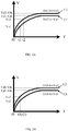
- FIG. 2A shows a voltage (that is, a sensing voltage) versus time curve C1 of the first electrode of the driving transistor in the first charging cycle and a voltage (that is, a sensing voltage) versus time curve C2 of the first electrode of the driving transistor in the second charging cycle.
- step S110 for example, the first data voltage Vd1 is applied to the gate electrode of the driving transistor at a start time t0 of the first charging cycle, and then in the first time duration (that is, t1-t0) after applying the first data voltage Vd1, the first sensing voltage Vs1 is obtained at the first electrode of the driving transistor, and it is determined whether the first sensing voltage Vs1 is equal to the first reference sensing voltage Vsr1.
- step S120 for example, the second data voltage Vd2 is applied to the gate electrode of the driving transistor at a start time t0 of the second charging cycle, and then in the second time duration (that is, t2-t0) after applying the second data voltage Vd2, the second sensing voltage Vs2 is obtained at the first electrode of the driving transistor, and it is determined whether the second sensing voltage Vs2 is equal to the second reference sensing voltage Vsr2.
- the second data voltage Vd2 is greater than the first data voltage Vd1, and the embodiments of the present disclosure include but are not limited thereto, for example, the second data voltage Vd2 may be smaller than the first data voltage Vd1.
- the first luminance value L1 and the second luminance value L2 are both specified (that is, pre-set) normalized luminance values.
- the maximum luminance value corresponding to the maximum data voltage is normalized to 1.
- first time duration (t1-t0) and the second time duration (t2-t0) may be set to be different, for example, as shown in FIG. 2A
- the first time duration (t1-t0) and the second time duration (t2-t0) may also be set to be the same.
- applying the first data voltage Vd1 or the second data voltage Vd2 to the gate electrode of the driving transistor means that a data voltage supplied through a data line of the pixel circuit (for example, the data line Vdat as shown in FIG. 6A or FIG. 6B ) is the first data voltage Vd1 or the second data voltage Vd2.
- the first electrode of the driving transistor refers to an electrode electrically connected with the sensing switch transistor T2, which may be a source electrode or a drain electrode according to a specific pixel circuit design.
- the first sensing voltage Vs1 is obtained in the first charging cycle and it is determined whether the first sensing voltage Vs1 is equal to the first reference sensing voltage Vsr1; and the second sensing voltage Vs2 is obtained in the second charging cycle and it is determined whether the second sensing voltage Vs2 is equal to the second reference sensing voltage Vsr2.
- the present current coefficient K of the driving transistor can be obtained according to the first formula and the present threshold voltage Vth of the driving transistor can be obtained according to the second formula, thereby completing the compensation detection of the pixel circuit, and improving the compensation effect and brightness uniformity of the display panel using the detecting method of the pixel circuit.
- the sensing voltages (the first sensing voltage Vs1 and the second sensing voltage Vs2) are obtained at the first electrode of the driving transistor before the driving transistor is turned off, thereby the detection time can be shortened, and the detection efficiency can be improved.
- the first sensing voltage Vs1 being equal to the first reference sensing voltage Vsr1 may mean that the first sensing voltage Vs1 is completely equal to the first reference sensing voltage Vsr1, thereby making the compensation data established for each pixel circuit more accurate.
- the first sensing voltage Vs1 being equal to the first reference sense Vsr1 may also mean that the difference between the first sensing voltage Vs1 and the first reference sensing voltage Vsr1 is less than a certain value (For example, less than 1% of the average value of the first sensing voltage Vs1 and the first reference sensing voltage Vsr1), thereby the detection time of the pixel circuit can be shortened.
- the description about the second sensing voltage Vs2 and the second reference sensing voltage Vsr2 is the same as that, and will not be described again.
- the detecting method provided by the embodiment of the present disclosure further includes the following operations:
- Vdrl represents the first reference data voltage
- Vdr2 represents the second reference data voltage
- Kr represents a reference current coefficient of the driving transistor
- Vthr represents a reference threshold voltage of the driving transistor
- L1 represents the first luminance value
- L2 represents the second luminance value.
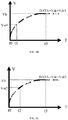
- FIG. 2C shows a voltage versus time curve C1' of the first electrode of the driving transistor in the first reference charging cycle and a voltage versus time curve C2' of the first electrode of the driving transistor in the second reference charging cycle.
- step S210 for example, the first reference data voltage Vdrl is applied to the gate electrode of the driving transistor at a start time t0 of the first reference charging cycle, and then in the first time duration (that is, t1-t0) after applying the first reference data voltage Vdr1, the first reference sensing voltage Vsr1 is obtained at the first electrode of the driving transistor.
- step S220 for example, the second reference data voltage Vdr2 is applied to the gate electrode of the driving transistor at a start time t0 of the second reference charging cycle, and then in second first time duration (that is, t2-t0) after applying the second reference data voltage Vdr2, the second reference sensing voltage Vsr2 is obtained at the first electrode of the driving transistor.
- second first time duration that is, t2-t0
- applying the first reference data voltage Vdrl or the second reference data voltage Vdr2 to the gate electrode of the driving transistor means that the data voltage supplied through the data line of the pixel circuit is the first reference data voltage Vdrl or the second reference data voltage Vdr2.
- the first reference charging cycle is prior to the first charging cycle.
- the first reference charging cycle may be in a power-off state of a corresponding display device during a power-off process, and the first charging cycle may be during the first power-on period of the corresponding display device after the first reference charging cycle, that is, during a startup period or a normal display period after the corresponding display device is powered on; for example, the first reference charging cycle may also be in a power-on state when the corresponding display device is powered on, that is, during the startup period after the power-on to the normal display, the first charging cycle may be during the power-on period after the first reference charging period.
- the first charging cycle may be between display periods of the normal display of the corresponding display device; the display periods each may be selected as various appropriate period, which is not specifically limited herein.
- the detecting method of the pixel circuit may further include the following operations: Step S140: in a third charging cycle, applying a third data voltage Vd3 to the gate electrode of the driving transistor, and in the first time duration after applying the third data voltage Vd3, obtaining a third sensing voltage Vs3 at the first electrode of the driving transistor.
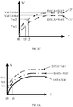
- FIG. 3A illustrates that, in a case where the first sensing voltage Vs1 is not equal to the first reference sensing voltage Vsr1 (for example, the first sensing voltage Vs1 is smaller than the first reference sensing voltage Vsr1), a voltage versus time curve of the first electrode of the driving transistor in the first reference charging cycle, a voltage versus time curve of the first electrode of the driving transistor in the first charging cycle, and a voltage versus time curve of the first electrode of the driving transistor in the third charging cycle.
- the third data voltage Vd3 is applied to the gate electrode of the driving transistor at a start time t0 of the third charging cycle, and then in the same first time duration (that is, t1-t0) after applying the third data voltage Vd3, the third sensing voltage Vs3 is obtained at the first electrode of the driving transistor. It should be noted that applying the third data voltage Vd3 to the gate electrode of the driving transistor means that the data voltage supplied through the data line of the pixel circuit is the third data voltage Vd3.
- a difference between the third sensing voltage Vs3 and the first reference sensing voltage Vsr1 may be made smaller than a difference between the first sensing voltage Vs1 and the first reference sensing voltage Vsr1 by selecting the third data voltage Vd3.
- the difference between the third sensing voltage Vs3 and the first reference sensing voltage Vsr1 refers to an absolute value
- the specific method of making the difference between the third sensing voltage Vs3 and the first reference sensing voltage Vsr1 smaller than the difference between the first sensing voltage Vs1 and the first reference sensing voltage Vsr1, by selecting the third data voltage Vd3, can be set according to actual conditions.
- the embodiments of the present disclosure do not limit this.
- the following method can be adopted to make the difference
- the sensing voltage can be increased by increasing the data voltage.
- the third sensing voltage Vs3 can be increased by making the third data voltage Vd3 larger than the first data voltage Vd1, so that the difference
- the third data voltage Vd3 can be made smaller than the first data voltage Vd1, such that the difference
- the detecting method of the pixel circuit further includes the following operation: Step S150: in a fourth charging cycle, applying a fourth data voltage Vd4 to the gate electrode of the driving transistor, and in the second time duration after applying the fourth data voltage Vd4, obtaining a fourth sensing voltage Vs4 at the first electrode of the driving transistor.
- FIG. 3B illustrates that, in the case where the second sensing voltage Vs2 is not equal to the second reference sensing voltage Vsr2 (for example, the second sensing voltage Vs2 is smaller than the second reference sensing voltage Vsr2), a voltage versus time curve of the first electrode of the driving transistor in the second reference charging cycle, a voltage versus time curve of the first electrode of the driving transistor in the second charging cycle, and a voltage versus time curve of the first electrode of the driving transistor in the fourth charging cycle.
- the fourth data voltage Vd4 is applied to the gate electrode of the driving transistor at a start time t0 of the fourth charging cycle, and then in the same second time duration (that is, t2-t0) after applying the fourth data voltage Vd4, the fourth sensing voltage Vs4 is obtained at the first electrode of the driving transistor. It should be noted that applying the fourth data voltage Vd4 to the gate electrode of the driving transistor means that the data voltage supplied through the data line of the pixel circuit is the fourth data voltage Vd4.
- a difference between the fourth sensing voltage Vs4 and the second reference sensing voltage Vsr2 may be made smaller than a difference between the second sensing voltage Vs2 and the second reference sensing voltage Vsr2 by selecting the fourth data voltage Vd4.
- the difference between the fourth sensing voltage Vs4 and the second reference sensing voltage Vsr2 refers to an absolute value
- the specific method of making the difference between the fourth sensing voltage Vs4 and the second reference sensing voltage Vsr2 smaller than the difference between the second sensing voltage Vs2 and the second reference sensing voltage Vsr2, by selecting the fourth data voltage Vd4, can be set according to actual conditions.
- the embodiments of the present disclosure do not limit this.
- the following method can be adopted to make the difference
- the sensing voltage can be increased by increasing the data voltage.
- the fourth sensing voltage Vs4 can be increased by making the fourth data voltage Vd4 larger than the second data voltage Vd2, so that the difference
- the fourth data voltage Vd4 can be made smaller than the second data voltage Vd2, such that the difference
- the first charging cycle and the third charging cycle may be between display periods in the power-on state.
- the third charging cycle may be after the first charging cycle.
- the first charging cycle and the third charging cycle can be respectively performed in different time interval between two sets of different frame images.
- the third charging cycle may be in a time interval between a period for displaying an (n)th frame image and a period for displaying an (n+1)th frame image (n is an integer greater than 3). In this way, the time interval between different frame images can be fully utilized for detection.
- the first charging cycle and the third charging cycle can be sequentially performed in the time interval between different frame images. For example, in a time interval between a period for displaying the third frame image and a period for displaying the fourth frame image, the first charging cycle and the third charging cycle are sequentially performed. In this way, the detection efficiency can be improved.
- the second charging cycle and the fourth charging cycle may be between the display periods in the power-on state.
- the fourth charging cycle may be after the second charging cycle.
- the second charging cycle and the fourth charging cycle can be respectively performed in different time interval between two sets of different frame images.
- the fourth charging cycle may be in the time interval between the period for displaying the (n)th frame image and the period for displaying the (n+1)th frame image (n is an integer greater than 3), however the embodiments of the present disclosure are not limited thereto. In this way, the time interval between different frame images can be fully utilized for detection.
- the second charging cycle and the fourth charging cycle can be sequentially performed in the time interval between different frame images.
- the second charging cycle and the fourth charging cycle are sequentially performed. In this way, the detection efficiency can be improved.
- the detecting method provided by the embodiment of the present disclosure further includes the following operations:
- the applied third data voltage Vd3 can be continuously adjusted by a successive approximation method until a sensing voltage equal to the first reference sensing voltage Vsr1 is finally obtained.
- repeating the third charging cycle means applying the adjusted third data voltage Vd3 to the gate electrode of the driving transistor in the other third charging cycle (for example, from Vd31 to Vd32, from Vd32 to Vd33...etc.), and in the first time duration after applying the third data voltage Vd3 and before the driving transistor is turned off, a new third sensing voltage Vs3 is obtained at the first electrode of the driving transistor (For example, in a case where the third data voltage Vd3 is Vd31, Vd32, and Vd33, respectively, the third sensing voltages Vs3 is Vs31, Vs32, and Vs33, respectively) to continuously reduce a difference
- the amount of change of the third data voltage Vd3 can be determined based on the difference
- the successive approximation method can also be used to continuously adjust the applied fourth data voltage Vd4 until finally obtaining a sensing voltage equal to the second reference sensing voltage Vsr2.
- repeating the fourth charging cycle means applying the adjusted fourth data voltage Vd4 to the gate electrode of the driving transistor in the other fourth charging cycle (for example, from Vd41 to Vd42, from Vd42 to Vd43...etc.), and in the first time duration after applying the fourth data voltage Vd4 and before the driving transistor is turned off, a new fourth sensing voltage Vs4 is obtained at the first electrode of the driving transistor (For example, in a case where the fourth data voltage Vd4 is Vd41, Vd42, and Vd43, respectively, the fourth sensing voltages Vs4 is Vs41, Vs42, and Vs43, respectively) to continuously reduce a difference
- the detecting method provided by the embodiment of the present disclosure further includes the following operation: Step S310: obtaining the reference threshold voltage Vthr and the reference current coefficient Kr.
- the method for obtaining the reference threshold voltage Vthr and the reference current coefficient Kr of the driving transistor can be set according to the actual situation, which is not limited by the embodiments of the present disclosure.
- the method for obtaining the reference threshold voltage Vthr and the reference current coefficient Kr will be exemplarily described below with reference to FIG. 5A to FIG. 5C .
- the power-off charging cycle can be made to be different from the first reference charging cycle or the second reference charging cycle, whereby only the acquired reference threshold voltage Vthr may be saved.
- the power-off data voltage Vdc may not be equal to the first reference data voltage Vdrl or the second reference data voltage Vdr2.
- the power-off charging cycle may be the same as the first reference charging cycle, that is, the power-off charging cycle and the first reference charging cycle are the same charging cycle.
- the power-off data voltage Vdc and the first reference data voltage Vdrl can be equal, whereby the detecting method of the pixel circuit can be simplified.
- the power-off charging cycle may be the same as the second reference charging cycle, that is, the power-off charging cycle and the second reference charging cycle are the same charging cycle.
- the power-off data voltage Vdc and the second reference data voltage Vdr2 can be equal, whereby the detecting method of the pixel circuit can be simplified.
- the present threshold voltage Vth of the pixel circuit is acquired while the present current coefficient K of the pixel circuit can be obtained, thereby completing the compensation detection of the pixel circuit, and the compensation effect and the brightness uniformity of the display panel, which is using the detecting method of the pixel circuit, can be improved.
- the detecting method of the pixel circuit provided by the embodiment of the present disclosure can be used to detect the threshold voltage and current coefficient of the driving transistor T3 (N-type transistor) in the pixel circuit as shown in FIG. 6A , but embodiments of the present disclosure are not limited thereto.
- the detecting method of the pixel circuit provided by the embodiment of the present disclosure can also be used to detect the threshold voltage and current coefficient of the driving transistor T3 (P-type transistor) in the pixel circuit as shown in FIG. 6B .
- the specific structure of the pixel circuit will be specifically described below by taking the pixel circuit as shown in FIG. 6A as an example, but the embodiments of the present disclosure do not limit this.
- the pixel circuit includes a driving transistor T3.
- the pixel circuit may further include a light emitting element EL and a sensing switch transistor T2.
- the light emitting element EL may be an organic light emitting diode, but the embodiments of the present disclosure are not limited thereto, and may be, for example, a quantum dot light emitting diode (QLED) or the like.
- QLED quantum dot light emitting diode
- a second electrode of the driving transistor T3 is configured to be connected with a first power supply voltage terminal VDD, for receiving a first voltage supplied by the first power supply voltage terminal VDD, and the first voltage may be, for example, a constant positive voltage; a first electrode of the driving transistor T3 is configured to be connected with a first electrode of the light emitting element EL.
- a second electrode of the light emitting element EL is connected with a second power supply voltage terminal VSS, the second power supply voltage terminal VSS can provide a constant voltage, for example, the voltage supplied by the second power supply voltage terminal VSS can be, for example, smaller than the voltage supplied by the first power supply voltage terminal VDD.
- the second power supply voltage terminal VSS can be grounded, for example, but the embodiments of the present disclosure do not limit this.
- a first electrode (a source electrode) of the sensing switch transistor T2 is electrically connected with the first electrode of the driving transistor T3.
- the pixel circuit further includes a sensing line SEN, a second electrode of the sensing switch transistor T2 is electrically connected with the sensing line SEN, and the sensing line SEN is electrically connected with, for example, a detecting circuit (not shown in FIG. 6A ).
- a detecting circuit not shown in FIG. 6A
- the pixel circuit further includes a data writing transistor T1 and a storage capacitor Cst, the data writing transistor T1 is configured to write a data signal to the gate electrode of the driving transistor T3 (for example, the first data voltage, the second data voltage, the first reference data voltage, and the second reference data voltage, etc.), and the storage capacitor Cst is configured to store the data signal.
- the pixel circuit further includes a data line Vdat, and a first electrode of the data writing transistor T1 is electrically connected with the data line Vdat.
- At least an embodiment of the present disclosure further provides a driving method of a display panel.
- the display panel includes a plurality of pixel circuits, and the pixel circuits included in the display panel are arranged, for example, in an array.
- each of the pixel circuits included in the display panel may be the pixel circuit as shown in FIG. 6A or 6B .
- the driving method includes the following operation:
- Step S410 performing the detecting method of the pixel circuit provided by any one of the embodiments of the present disclosure on the pixel circuit for obtaining a present threshold voltage Vth and a present current coefficient K of the driving transistor T3 of the pixel circuit.
- the detecting method of the pixel circuit can be referred to the corresponding description in the above embodiment, and details are not described herein again.
- the driving method of the display panel provided by the embodiment of the present disclosure further includes the following operation:
- Vc represents the compensation data voltage
- K represents the present current coefficient
- Vth represents the present threshold voltage
- L represents a normalized luminance value to be displayed by the pixel circuit.
- the present threshold voltage and the present current coefficient of the driving transistor T3 of the pixel circuit can be detected row by row, and then, after obtaining the present threshold voltages and the present current coefficients of the driving transistors T3 of all the pixel circuits of the display panel, the compensation data voltage can be established for each pixel circuit, and finally, based on the established compensation data voltage, data compensation is performed on the display panel, thereby completing one cycle of data compensation.
- the detecting method of the pixel circuit provided by any one of the embodiments of the present disclosure can be performed on pixel circuits located in the first row, and the present threshold voltages and the present current coefficients of the driving transistors T3 of the pixel circuits located in the first row are obtained; then, the detecting method of the pixel circuit provided by any one of the embodiments of the present disclosure can be performed on the pixel circuits located in the second row, and the present threshold voltages and the present current coefficients of the driving transistors T3 of the pixel circuits located in the second row are obtained; and then, the pixel circuits of the display panel located in other rows are performed by line-by-line detection until the present threshold voltages and present current coefficients of the driving transistors T3 of all the pixel circuits of the display panel are obtained; finally, the compensation data voltage is established for each pixel circuit, and data compensation is performed on the display panel.
- a compensation data voltage is established for each pixel circuit of the row, and then data compensation is performed on the pixel circuits located in the row.
- detecting, establishing compensation data voltages and data compensating are performed on the pixel circuits of the first row; and then, the detecting, establishing compensation data voltages and data compensating are performed on the pixel circuits of a fifth row; and then, the detecting, establishing compensation data voltages and data compensating are performed on the pixel circuits of the second row until the detecting, establishing compensation data voltages and data compensating are performed on all the pixel circuits of the display panel, thereby realizing one cycle of data compensation for the display panel.
- the driving method of the display panel provided by the embodiment of the present disclosure can implement detection of the present threshold voltage and the present current coefficient of the driving transistor T3 during a power-on period (for example, between adjacent display cycles), thereby realizing a real-time compensation, and can further improve the compensation effect and the brightness uniformity of the display panel to which the driving method is applied.
- At least one embodiment of the present disclosure further provides a display device including a pixel circuit and a control circuit.
- the pixel circuit may be the pixel circuit as shown in FIG. 6A or 6B .
- the display device provided by the embodiment of the present disclosure is specifically described below by taking the pixel circuit as shown in FIG. 6A as an example, but the embodiments of the present disclosure are not limited thereto.
- FIG. 8 shows a schematic diagram of a display device 10.
- the display device 10 includes a pixel circuit 110 and a control circuit 120, and the pixel circuit 110 includes a driving transistor T3.
- the control circuit 120 is configured to perform the detecting method of the pixel circuit provided by the embodiment of the present disclosure, that is, the control circuit 120 can be configured to perform or partially perform steps S110, S120, S130, S140, S150, S160, S170, S180, S210, S220, S230, S310, S301, S302, and the like in the above embodiment.
- the display device 10 further includes a data driving circuit 130, a detecting circuit 140 and a scan driving circuit (not shown in FIG. 8 ).
- the control circuit 120 can further be configured to control the data driving circuit 130 and the detecting circuit 140.
- the data driving circuit 130 is configured to output the first reference data voltage, the second reference data voltage, the first data voltage, the second data voltage, the third data voltage, and the fourth data voltage, etc., at different times.
- the scan driving circuit outputs the scanning signal for the data writing transistor T1 and the sensing transistor T2.
- the scan driving circuit can be connected with the gate electrode G1 of the data writing transistor T1 and the gate electrode G2 of the sensing transistor T2 to provide a corresponding scanning signal, thereby controlling the turn-on and turn-off of the data writing transistor T1 and the sensing transistor T2.
- the pixel circuit is further configured to receive the first reference data voltage, the second reference data voltage, the first data voltage, the second data voltage, the third data voltage, and the fourth data voltage, etc., and apply one of the first reference data voltage, the second reference data voltage, the first data voltage, the second data voltage, the third data voltage and the fourth data voltage to the gate electrode of the driving transistor T3.
- the detecting circuit 140 is configured to read the first reference sensing voltage, the second reference sensing voltage, the first sensing voltage, the second sensing voltage, the third sensing voltage, and the fourth sensing voltage, etc. from the first electrode of the driving transistor T3.
- the data driving circuit 130 can be further configured to provide the power-off data voltage
- the pixel circuit can be further configured to receive the power-off data voltage and apply the power-off data voltage to the gate electrode of the driving transistor T3
- the detecting circuit 140 can further be configured to read a turn-off sensing voltage from the first electrode of the driving transistor T3.
- the pixel circuit further includes a light emitting element EL and a sensing switch transistor T2, and the light emitting element EL may be, for example, an organic light emitting diode, but the embodiments of the present disclosure are not limited thereto, and may be, for example, a quantum dot light emitting diode (QLED) or the like.
- the second electrode of the driving transistor T3 and the first electrode of the driving transistor T3 are configured to be connected with the first power supply voltage terminal VDD and a first electrode of the light emitting element EL, respectively, and a second electrode of the light emitting element EL is connected with the second power supply voltage terminal VSS.
- a first electrode of the sensing switch transistor T2 is electrically connected with the first electrode of the driving transistor T3, and a second electrode of the sensing switch transistor T2 is electrically connected with the detecting circuit 140.
- the pixel circuit further includes a sensing line SEN, and the sensing line SEN electrically connects the second electrode of the sensing switch transistor T2 with the detecting circuit 140.
- the pixel circuit further includes a data writing transistor T1 and a storage capacitor Cst, the data writing transistor T1 is configured to obtain a data voltage from the data driving circuit 130 and write the data voltage to the gate electrode of the driving transistor T3, and the storage capacitor Cst stores the data voltage.
- the pixel circuit further includes a data line Vdat, and the first electrode of the data writing transistor T1 is connected with the data line Vdat.
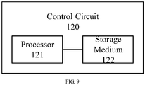
- the control circuit 120 includes a processor 121 and a storage medium 122, the storage medium 122 is configured to store computer instructions executable by the processor 121, and the computer instructions are capable of being executed by the processor 121 to implement the detecting method provided by the embodiments of the present disclosure.
- the processor 121 is, for example, a central processing unit (CPU) or other processing units with a data processing ability and/or instruction execution ability.
- the processor may be implemented as a general processor, or may also be implemented as a single chip microcomputer, a microprocessor, a digital signal processor, a dedicated image processing chip, a field programmable logic array, or the like.
- the storage medium 122 includes a volatile memory and/or a nonvolatile memory, and for example, includes a read only memory (ROM), a hard disk, a flash memory, or the like.
- the storage medium may be implemented as one or a plurality of computer program products, which may include various forms of computer-readable storage medium, and one or a plurality of executable codes (for example, computer program instructions) can be stored in the computer-readable storage medium.
- the processor can execute the program instructions to perform the detecting method provided by the embodiment of the present disclosure, thereby obtaining the present threshold voltage and the present current coefficient of the driving transistor of the pixel circuit included in the display device, thereby implementing the data compensation function of the display device.
- the storage medium may further store various other applications and various data, such as the reference threshold voltage and/or the reference current coefficient of each pixel circuit, as well as various data used and/or generated by the applications, or the like.
- the display device provided by the embodiment of the present disclosure can implement detection of the present threshold voltage and the present current coefficient of the driving transistor during a power-on period (for example, between adjacent display cycles), thereby realizing a real-time detection and a real-time compensation during the power-on period of the display device, and can further improve the compensation effect and the brightness uniformity of the display device.
Landscapes
- Engineering & Computer Science (AREA)
- Physics & Mathematics (AREA)
- Computer Hardware Design (AREA)
- General Physics & Mathematics (AREA)
- Theoretical Computer Science (AREA)
- Control Of Indicators Other Than Cathode Ray Tubes (AREA)
- Control Of El Displays (AREA)
- Electroluminescent Light Sources (AREA)
Applications Claiming Priority (2)
| Application Number | Priority Date | Filing Date | Title |
|---|---|---|---|
| CN201810085782.1A CN110097840B (zh) | 2018-01-29 | 2018-01-29 | 像素电路的检测方法、显示面板的驱动方法和显示装置 |
| PCT/CN2018/112954 WO2019144669A1 (fr) | 2018-01-29 | 2018-10-31 | Procédé de détection pour circuit de pixel, procédé d'excitation pour écran d'affichage et dispositif d'affichage |
Publications (2)
| Publication Number | Publication Date |
|---|---|
| EP3748618A1 true EP3748618A1 (fr) | 2020-12-09 |
| EP3748618A4 EP3748618A4 (fr) | 2021-10-13 |
Family
ID=67395143
Family Applications (1)
| Application Number | Title | Priority Date | Filing Date |
|---|---|---|---|
| EP18882298.5A Withdrawn EP3748618A4 (fr) | 2018-01-29 | 2018-10-31 | Procédé de détection pour circuit de pixel, procédé d'excitation pour écran d'affichage et dispositif d'affichage |
Country Status (4)
| Country | Link |
|---|---|
| US (1) | US11776438B2 (fr) |
| EP (1) | EP3748618A4 (fr) |
| CN (1) | CN110097840B (fr) |
| WO (1) | WO2019144669A1 (fr) |
Families Citing this family (5)
| Publication number | Priority date | Publication date | Assignee | Title |
|---|---|---|---|---|
| CN112967680B (zh) * | 2021-03-18 | 2022-12-16 | 合肥京东方卓印科技有限公司 | 像素结构及其驱动方法、显示基板 |
| KR102887311B1 (ko) * | 2021-08-13 | 2025-11-17 | 엘지디스플레이 주식회사 | 디스플레이 장치, 데이터 구동 회로 및 디스플레이 구동 방법 |
| CN113808529B (zh) * | 2021-09-28 | 2023-03-21 | 深圳市华星光电半导体显示技术有限公司 | 像素电路及其外部补偿方法 |
| CN116312378A (zh) * | 2023-03-30 | 2023-06-23 | 京东方科技集团股份有限公司 | 像素电路、显示基板及像素驱动方法 |
| TWI900162B (zh) * | 2024-08-07 | 2025-10-01 | 超炫科技股份有限公司 | 電致發光顯示器之像素電路 |
Family Cites Families (15)
| Publication number | Priority date | Publication date | Assignee | Title |
|---|---|---|---|---|
| JP2009060282A (ja) * | 2007-08-30 | 2009-03-19 | Kyocera Corp | 携帯電子機器及び表示輝度制御方法 |
| CN101923829A (zh) * | 2010-06-30 | 2010-12-22 | 昆山工研院新型平板显示技术中心有限公司 | 一种有源矩阵有机发光显示器 |
| CN103093724A (zh) * | 2013-03-04 | 2013-05-08 | 陈鑫 | 一种新型的amoled像素驱动电路 |
| CN104157234A (zh) * | 2014-01-17 | 2014-11-19 | 北京京东方光电科技有限公司 | 像素单元驱动电路及方法、显示装置 |
| CN105225621B (zh) * | 2014-06-25 | 2020-08-25 | 伊格尼斯创新公司 | 提取有机发光器件的相关曲线的系统和方法 |
| KR101789602B1 (ko) * | 2014-12-31 | 2017-10-26 | 엘지디스플레이 주식회사 | 유기발광 표시장치 및 그의 구동 방법 |
| CN104700761B (zh) * | 2015-04-03 | 2017-08-29 | 京东方科技集团股份有限公司 | 一种检测电路及其检测方法和驱动系统 |
| KR102301325B1 (ko) * | 2015-06-30 | 2021-09-14 | 엘지디스플레이 주식회사 | 유기발광 표시장치에 구비된 구동 tft의 문턱전압 센싱장치 및 센싱방법 |
| CN105047137B (zh) * | 2015-09-09 | 2017-05-31 | 深圳市华星光电技术有限公司 | Amoled实时补偿系统 |
| CN106847187B (zh) * | 2017-03-01 | 2019-04-05 | 上海天马有机发光显示技术有限公司 | 一种像素电路的电流检测方法、显示面板以及显示装置 |
| CN108877686B (zh) * | 2017-05-12 | 2020-12-08 | 京东方科技集团股份有限公司 | 数据补偿方法及装置、显示驱动方法及装置、显示装置 |
| CN107093403B (zh) | 2017-06-30 | 2019-03-15 | 深圳市华星光电技术有限公司 | 用于oled显示面板的像素驱动电路的补偿方法 |
| CN109697944B (zh) | 2017-10-20 | 2020-11-24 | 京东方科技集团股份有限公司 | 像素电路的检测方法、显示面板的驱动方法和显示装置 |
| CN107610629B (zh) * | 2017-11-06 | 2019-07-09 | 合肥鑫晟光电科技有限公司 | 阵列基板驱动电路的检测方法 |
| CN107749280A (zh) * | 2017-12-06 | 2018-03-02 | 京东方科技集团股份有限公司 | 显示装置的驱动方法及显示装置 |
-
2018
- 2018-01-29 CN CN201810085782.1A patent/CN110097840B/zh active Active
- 2018-10-31 WO PCT/CN2018/112954 patent/WO2019144669A1/fr not_active Ceased
- 2018-10-31 EP EP18882298.5A patent/EP3748618A4/fr not_active Withdrawn
- 2018-10-31 US US16/467,022 patent/US11776438B2/en active Active
Also Published As
| Publication number | Publication date |
|---|---|
| US11776438B2 (en) | 2023-10-03 |
| US20230206792A1 (en) | 2023-06-29 |
| WO2019144669A1 (fr) | 2019-08-01 |
| CN110097840A (zh) | 2019-08-06 |
| CN110097840B (zh) | 2021-11-16 |
| EP3748618A4 (fr) | 2021-10-13 |
Similar Documents
| Publication | Publication Date | Title |
|---|---|---|
| US20220366851A1 (en) | Pixel circuit, driving method thereof and display device | |
| US10417961B2 (en) | Organic light-emitting display panel and driving method thereof, organic light-emitting display device | |
| CN110520922B (zh) | 显示驱动电路、方法、以及显示设备 | |
| US10818239B2 (en) | Pixel driving circuit and method for driving the same, pixel unit and display panel | |
| US10825396B2 (en) | Pixel driving circuit and method for controlling the same, display driving circuit and method for controlling the same, and display panel | |
| JP5183336B2 (ja) | 表示装置 | |
| US11308889B2 (en) | Detection method of pixel circuit, driving method of display panel, and display device | |
| US9214506B2 (en) | Pixel unit driving circuit, method for driving pixel unit driving circuit and display device | |
| CN111105751B (zh) | 显示设备、用于驱动显示设备的方法以及电子装置 | |
| US9633604B2 (en) | Display device, method for driving display device, and electronic apparatus | |
| US9928776B2 (en) | Readout circuit and organic light emitting display device having the same | |
| US20170243542A1 (en) | Organic light-emitting display panel, driving method thereof, and organic light-emitting display device | |
| US20170278457A1 (en) | Organic Light-Emitting Pixel Driving Circuit, Driving Method And Organic Light-Emitting Display Device | |
| US11127342B2 (en) | Pixel circuit for driving light emitting diode to emit light and method of controlling the pixel circuit | |
| EP3748618A1 (fr) | Procédé de détection pour circuit de pixel, procédé d'excitation pour écran d'affichage et dispositif d'affichage | |
| US9947267B2 (en) | Light emitting diode pixel unit circuit and display panel for light emitting diode display | |
| JP6175718B2 (ja) | 駆動方法および表示装置 | |
| JP2009265459A (ja) | 画素回路および表示装置 | |
| EP2161707A1 (fr) | Appareil d'affichage | |
| CN110060631A (zh) | 像素电路 | |
| US8519919B2 (en) | Display device and method to prevent the change of threshold voltage of the writing transistor due to the variation with age | |
| TWI685833B (zh) | 畫素電路 | |
| CN101069226B (zh) | 图像显示装置及其驱动方法 | |
| JP2010026209A (ja) | 表示装置 |
Legal Events
| Date | Code | Title | Description |
|---|---|---|---|
| STAA | Information on the status of an ep patent application or granted ep patent |
Free format text: STATUS: UNKNOWN |
|
| STAA | Information on the status of an ep patent application or granted ep patent |
Free format text: STATUS: THE INTERNATIONAL PUBLICATION HAS BEEN MADE |
|
| PUAI | Public reference made under article 153(3) epc to a published international application that has entered the european phase |
Free format text: ORIGINAL CODE: 0009012 |
|
| STAA | Information on the status of an ep patent application or granted ep patent |
Free format text: STATUS: REQUEST FOR EXAMINATION WAS MADE |
|
| 17P | Request for examination filed |
Effective date: 20190606 |
|
| AK | Designated contracting states |
Kind code of ref document: A1 Designated state(s): AL AT BE BG CH CY CZ DE DK EE ES FI FR GB GR HR HU IE IS IT LI LT LU LV MC MK MT NL NO PL PT RO RS SE SI SK SM TR |
|
| AX | Request for extension of the european patent |
Extension state: BA ME |
|
| DAV | Request for validation of the european patent (deleted) | ||
| DAX | Request for extension of the european patent (deleted) | ||
| RIN1 | Information on inventor provided before grant (corrected) |
Inventor name: SONG, DANNA |
|
| A4 | Supplementary search report drawn up and despatched |
Effective date: 20210914 |
|
| RIC1 | Information provided on ipc code assigned before grant |
Ipc: G09G 3/3233 20160101ALI20210908BHEP Ipc: G09G 3/00 20060101AFI20210908BHEP |
|
| STAA | Information on the status of an ep patent application or granted ep patent |
Free format text: STATUS: EXAMINATION IS IN PROGRESS |
|
| 17Q | First examination report despatched |
Effective date: 20230915 |
|
| STAA | Information on the status of an ep patent application or granted ep patent |
Free format text: STATUS: THE APPLICATION HAS BEEN WITHDRAWN |
|
| 18W | Application withdrawn |
Effective date: 20231013 |