EP3748623B1 - Anzeigevorrichtung und verfahren zur steuerung davon - Google Patents
Anzeigevorrichtung und verfahren zur steuerung davon Download PDFInfo
- Publication number
- EP3748623B1 EP3748623B1 EP20177221.7A EP20177221A EP3748623B1 EP 3748623 B1 EP3748623 B1 EP 3748623B1 EP 20177221 A EP20177221 A EP 20177221A EP 3748623 B1 EP3748623 B1 EP 3748623B1
- Authority
- EP
- European Patent Office
- Prior art keywords
- gate
- voltage
- screen
- screen part
- signal
- Prior art date
- Legal status (The legal status is an assumption and is not a legal conclusion. Google has not performed a legal analysis and makes no representation as to the accuracy of the status listed.)
- Active
Links
Images


















Classifications
-
- G—PHYSICS
- G09—EDUCATION; CRYPTOGRAPHY; DISPLAY; ADVERTISING; SEALS
- G09F—DISPLAYING; ADVERTISING; SIGNS; LABELS OR NAME-PLATES; SEALS
- G09F9/00—Indicating arrangements for variable information in which the information is built-up on a support by selection or combination of individual elements
- G09F9/30—Indicating arrangements for variable information in which the information is built-up on a support by selection or combination of individual elements in which the desired character or characters are formed by combining individual elements
- G09F9/301—Indicating arrangements for variable information in which the information is built-up on a support by selection or combination of individual elements in which the desired character or characters are formed by combining individual elements flexible foldable or roll-able electronic displays, e.g. thin LCD, OLED
-
- G—PHYSICS
- G09—EDUCATION; CRYPTOGRAPHY; DISPLAY; ADVERTISING; SEALS
- G09G—ARRANGEMENTS OR CIRCUITS FOR CONTROL OF INDICATING DEVICES USING STATIC MEANS TO PRESENT VARIABLE INFORMATION
- G09G3/00—Control arrangements or circuits, of interest only in connection with visual indicators other than cathode-ray tubes
- G09G3/03—Control arrangements or circuits, of interest only in connection with visual indicators other than cathode-ray tubes specially adapted for displays having non-planar surfaces, e.g. curved displays
- G09G3/035—Control arrangements or circuits, of interest only in connection with visual indicators other than cathode-ray tubes specially adapted for displays having non-planar surfaces, e.g. curved displays for flexible display surfaces
-
- G—PHYSICS
- G09—EDUCATION; CRYPTOGRAPHY; DISPLAY; ADVERTISING; SEALS
- G09G—ARRANGEMENTS OR CIRCUITS FOR CONTROL OF INDICATING DEVICES USING STATIC MEANS TO PRESENT VARIABLE INFORMATION
- G09G3/00—Control arrangements or circuits, of interest only in connection with visual indicators other than cathode-ray tubes
- G09G3/20—Control arrangements or circuits, of interest only in connection with visual indicators other than cathode-ray tubes for presentation of an assembly of a number of characters, e.g. a page, by composing the assembly by combination of individual elements arranged in a matrix no fixed position being assigned to or needed to be assigned to the individual characters or partial characters
- G09G3/22—Control arrangements or circuits, of interest only in connection with visual indicators other than cathode-ray tubes for presentation of an assembly of a number of characters, e.g. a page, by composing the assembly by combination of individual elements arranged in a matrix no fixed position being assigned to or needed to be assigned to the individual characters or partial characters using controlled light sources
- G09G3/30—Control arrangements or circuits, of interest only in connection with visual indicators other than cathode-ray tubes for presentation of an assembly of a number of characters, e.g. a page, by composing the assembly by combination of individual elements arranged in a matrix no fixed position being assigned to or needed to be assigned to the individual characters or partial characters using controlled light sources using electroluminescent panels
- G09G3/32—Control arrangements or circuits, of interest only in connection with visual indicators other than cathode-ray tubes for presentation of an assembly of a number of characters, e.g. a page, by composing the assembly by combination of individual elements arranged in a matrix no fixed position being assigned to or needed to be assigned to the individual characters or partial characters using controlled light sources using electroluminescent panels semiconductive, e.g. using light-emitting diodes [LED]
- G09G3/3208—Control arrangements or circuits, of interest only in connection with visual indicators other than cathode-ray tubes for presentation of an assembly of a number of characters, e.g. a page, by composing the assembly by combination of individual elements arranged in a matrix no fixed position being assigned to or needed to be assigned to the individual characters or partial characters using controlled light sources using electroluminescent panels semiconductive, e.g. using light-emitting diodes [LED] organic, e.g. using organic light-emitting diodes [OLED]
- G09G3/3225—Control arrangements or circuits, of interest only in connection with visual indicators other than cathode-ray tubes for presentation of an assembly of a number of characters, e.g. a page, by composing the assembly by combination of individual elements arranged in a matrix no fixed position being assigned to or needed to be assigned to the individual characters or partial characters using controlled light sources using electroluminescent panels semiconductive, e.g. using light-emitting diodes [LED] organic, e.g. using organic light-emitting diodes [OLED] using an active matrix
-
- G—PHYSICS
- G09—EDUCATION; CRYPTOGRAPHY; DISPLAY; ADVERTISING; SEALS
- G09G—ARRANGEMENTS OR CIRCUITS FOR CONTROL OF INDICATING DEVICES USING STATIC MEANS TO PRESENT VARIABLE INFORMATION
- G09G3/00—Control arrangements or circuits, of interest only in connection with visual indicators other than cathode-ray tubes
- G09G3/20—Control arrangements or circuits, of interest only in connection with visual indicators other than cathode-ray tubes for presentation of an assembly of a number of characters, e.g. a page, by composing the assembly by combination of individual elements arranged in a matrix no fixed position being assigned to or needed to be assigned to the individual characters or partial characters
- G09G3/22—Control arrangements or circuits, of interest only in connection with visual indicators other than cathode-ray tubes for presentation of an assembly of a number of characters, e.g. a page, by composing the assembly by combination of individual elements arranged in a matrix no fixed position being assigned to or needed to be assigned to the individual characters or partial characters using controlled light sources
- G09G3/30—Control arrangements or circuits, of interest only in connection with visual indicators other than cathode-ray tubes for presentation of an assembly of a number of characters, e.g. a page, by composing the assembly by combination of individual elements arranged in a matrix no fixed position being assigned to or needed to be assigned to the individual characters or partial characters using controlled light sources using electroluminescent panels
- G09G3/32—Control arrangements or circuits, of interest only in connection with visual indicators other than cathode-ray tubes for presentation of an assembly of a number of characters, e.g. a page, by composing the assembly by combination of individual elements arranged in a matrix no fixed position being assigned to or needed to be assigned to the individual characters or partial characters using controlled light sources using electroluminescent panels semiconductive, e.g. using light-emitting diodes [LED]
- G09G3/3208—Control arrangements or circuits, of interest only in connection with visual indicators other than cathode-ray tubes for presentation of an assembly of a number of characters, e.g. a page, by composing the assembly by combination of individual elements arranged in a matrix no fixed position being assigned to or needed to be assigned to the individual characters or partial characters using controlled light sources using electroluminescent panels semiconductive, e.g. using light-emitting diodes [LED] organic, e.g. using organic light-emitting diodes [OLED]
- G09G3/3225—Control arrangements or circuits, of interest only in connection with visual indicators other than cathode-ray tubes for presentation of an assembly of a number of characters, e.g. a page, by composing the assembly by combination of individual elements arranged in a matrix no fixed position being assigned to or needed to be assigned to the individual characters or partial characters using controlled light sources using electroluminescent panels semiconductive, e.g. using light-emitting diodes [LED] organic, e.g. using organic light-emitting diodes [OLED] using an active matrix
- G09G3/3233—Control arrangements or circuits, of interest only in connection with visual indicators other than cathode-ray tubes for presentation of an assembly of a number of characters, e.g. a page, by composing the assembly by combination of individual elements arranged in a matrix no fixed position being assigned to or needed to be assigned to the individual characters or partial characters using controlled light sources using electroluminescent panels semiconductive, e.g. using light-emitting diodes [LED] organic, e.g. using organic light-emitting diodes [OLED] using an active matrix with pixel circuitry controlling the current through the light-emitting element
-
- G—PHYSICS
- G09—EDUCATION; CRYPTOGRAPHY; DISPLAY; ADVERTISING; SEALS
- G09G—ARRANGEMENTS OR CIRCUITS FOR CONTROL OF INDICATING DEVICES USING STATIC MEANS TO PRESENT VARIABLE INFORMATION
- G09G3/00—Control arrangements or circuits, of interest only in connection with visual indicators other than cathode-ray tubes
- G09G3/20—Control arrangements or circuits, of interest only in connection with visual indicators other than cathode-ray tubes for presentation of an assembly of a number of characters, e.g. a page, by composing the assembly by combination of individual elements arranged in a matrix no fixed position being assigned to or needed to be assigned to the individual characters or partial characters
- G09G3/22—Control arrangements or circuits, of interest only in connection with visual indicators other than cathode-ray tubes for presentation of an assembly of a number of characters, e.g. a page, by composing the assembly by combination of individual elements arranged in a matrix no fixed position being assigned to or needed to be assigned to the individual characters or partial characters using controlled light sources
- G09G3/30—Control arrangements or circuits, of interest only in connection with visual indicators other than cathode-ray tubes for presentation of an assembly of a number of characters, e.g. a page, by composing the assembly by combination of individual elements arranged in a matrix no fixed position being assigned to or needed to be assigned to the individual characters or partial characters using controlled light sources using electroluminescent panels
- G09G3/32—Control arrangements or circuits, of interest only in connection with visual indicators other than cathode-ray tubes for presentation of an assembly of a number of characters, e.g. a page, by composing the assembly by combination of individual elements arranged in a matrix no fixed position being assigned to or needed to be assigned to the individual characters or partial characters using controlled light sources using electroluminescent panels semiconductive, e.g. using light-emitting diodes [LED]
- G09G3/3208—Control arrangements or circuits, of interest only in connection with visual indicators other than cathode-ray tubes for presentation of an assembly of a number of characters, e.g. a page, by composing the assembly by combination of individual elements arranged in a matrix no fixed position being assigned to or needed to be assigned to the individual characters or partial characters using controlled light sources using electroluminescent panels semiconductive, e.g. using light-emitting diodes [LED] organic, e.g. using organic light-emitting diodes [OLED]
- G09G3/3266—Details of drivers for scan electrodes
-
- G—PHYSICS
- G09—EDUCATION; CRYPTOGRAPHY; DISPLAY; ADVERTISING; SEALS
- G09G—ARRANGEMENTS OR CIRCUITS FOR CONTROL OF INDICATING DEVICES USING STATIC MEANS TO PRESENT VARIABLE INFORMATION
- G09G5/00—Control arrangements or circuits for visual indicators common to cathode-ray tube indicators and other visual indicators
- G09G5/14—Display of multiple viewports
-
- G—PHYSICS
- G09—EDUCATION; CRYPTOGRAPHY; DISPLAY; ADVERTISING; SEALS
- G09G—ARRANGEMENTS OR CIRCUITS FOR CONTROL OF INDICATING DEVICES USING STATIC MEANS TO PRESENT VARIABLE INFORMATION
- G09G5/00—Control arrangements or circuits for visual indicators common to cathode-ray tube indicators and other visual indicators
- G09G5/36—Control arrangements or circuits for visual indicators common to cathode-ray tube indicators and other visual indicators characterised by the display of a graphic pattern, e.g. using an all-points-addressable [APA] memory
- G09G5/37—Details of the operation on graphic patterns
- G09G5/373—Details of the operation on graphic patterns for modifying the size of the graphic pattern
-
- G—PHYSICS
- G09—EDUCATION; CRYPTOGRAPHY; DISPLAY; ADVERTISING; SEALS
- G09G—ARRANGEMENTS OR CIRCUITS FOR CONTROL OF INDICATING DEVICES USING STATIC MEANS TO PRESENT VARIABLE INFORMATION
- G09G2300/00—Aspects of the constitution of display devices
- G09G2300/02—Composition of display devices
- G09G2300/026—Video wall, i.e. juxtaposition of a plurality of screens to create a display screen of bigger dimensions
-
- G—PHYSICS
- G09—EDUCATION; CRYPTOGRAPHY; DISPLAY; ADVERTISING; SEALS
- G09G—ARRANGEMENTS OR CIRCUITS FOR CONTROL OF INDICATING DEVICES USING STATIC MEANS TO PRESENT VARIABLE INFORMATION
- G09G2300/00—Aspects of the constitution of display devices
- G09G2300/08—Active matrix structure, i.e. with use of active elements, inclusive of non-linear two terminal elements, in the pixels together with light emitting or modulating elements
- G09G2300/0809—Several active elements per pixel in active matrix panels
-
- G—PHYSICS
- G09—EDUCATION; CRYPTOGRAPHY; DISPLAY; ADVERTISING; SEALS
- G09G—ARRANGEMENTS OR CIRCUITS FOR CONTROL OF INDICATING DEVICES USING STATIC MEANS TO PRESENT VARIABLE INFORMATION
- G09G2310/00—Command of the display device
- G09G2310/02—Addressing, scanning or driving the display screen or processing steps related thereto
- G09G2310/0202—Addressing of scan or signal lines
- G09G2310/0221—Addressing of scan or signal lines with use of split matrices
-
- G—PHYSICS
- G09—EDUCATION; CRYPTOGRAPHY; DISPLAY; ADVERTISING; SEALS
- G09G—ARRANGEMENTS OR CIRCUITS FOR CONTROL OF INDICATING DEVICES USING STATIC MEANS TO PRESENT VARIABLE INFORMATION
- G09G2330/00—Aspects of power supply; Aspects of display protection and defect management
- G09G2330/02—Details of power systems and of start or stop of display operation
- G09G2330/021—Power management, e.g. power saving
-
- G—PHYSICS
- G09—EDUCATION; CRYPTOGRAPHY; DISPLAY; ADVERTISING; SEALS
- G09G—ARRANGEMENTS OR CIRCUITS FOR CONTROL OF INDICATING DEVICES USING STATIC MEANS TO PRESENT VARIABLE INFORMATION
- G09G2330/00—Aspects of power supply; Aspects of display protection and defect management
- G09G2330/02—Details of power systems and of start or stop of display operation
- G09G2330/021—Power management, e.g. power saving
- G09G2330/022—Power management, e.g. power saving in absence of operation, e.g. no data being entered during a predetermined time
-
- G—PHYSICS
- G09—EDUCATION; CRYPTOGRAPHY; DISPLAY; ADVERTISING; SEALS
- G09G—ARRANGEMENTS OR CIRCUITS FOR CONTROL OF INDICATING DEVICES USING STATIC MEANS TO PRESENT VARIABLE INFORMATION
- G09G2330/00—Aspects of power supply; Aspects of display protection and defect management
- G09G2330/02—Details of power systems and of start or stop of display operation
- G09G2330/021—Power management, e.g. power saving
- G09G2330/023—Power management, e.g. power saving using energy recovery or conservation
-
- G—PHYSICS
- G09—EDUCATION; CRYPTOGRAPHY; DISPLAY; ADVERTISING; SEALS
- G09G—ARRANGEMENTS OR CIRCUITS FOR CONTROL OF INDICATING DEVICES USING STATIC MEANS TO PRESENT VARIABLE INFORMATION
- G09G2330/00—Aspects of power supply; Aspects of display protection and defect management
- G09G2330/02—Details of power systems and of start or stop of display operation
- G09G2330/028—Generation of voltages supplied to electrode drivers in a matrix display other than LCD
-
- G—PHYSICS
- G09—EDUCATION; CRYPTOGRAPHY; DISPLAY; ADVERTISING; SEALS
- G09G—ARRANGEMENTS OR CIRCUITS FOR CONTROL OF INDICATING DEVICES USING STATIC MEANS TO PRESENT VARIABLE INFORMATION
- G09G2340/00—Aspects of display data processing
- G09G2340/04—Changes in size, position or resolution of an image
- G09G2340/0407—Resolution change, inclusive of the use of different resolutions for different screen areas
-
- G—PHYSICS
- G09—EDUCATION; CRYPTOGRAPHY; DISPLAY; ADVERTISING; SEALS
- G09G—ARRANGEMENTS OR CIRCUITS FOR CONTROL OF INDICATING DEVICES USING STATIC MEANS TO PRESENT VARIABLE INFORMATION
- G09G2340/00—Aspects of display data processing
- G09G2340/04—Changes in size, position or resolution of an image
- G09G2340/0407—Resolution change, inclusive of the use of different resolutions for different screen areas
- G09G2340/0435—Change or adaptation of the frame rate of the video stream
-
- G—PHYSICS
- G09—EDUCATION; CRYPTOGRAPHY; DISPLAY; ADVERTISING; SEALS
- G09G—ARRANGEMENTS OR CIRCUITS FOR CONTROL OF INDICATING DEVICES USING STATIC MEANS TO PRESENT VARIABLE INFORMATION
- G09G2380/00—Specific applications
- G09G2380/02—Flexible displays
Definitions
- the present disclosure relates to a display device in which a screen is capable of being folded using a flexible display panel, and to a method for controlling the same.
- the organic light emitting display devices do not require backlight units and may be implemented on a flexible substrate made of a plastic substrate, a thin glass substrate, or a metal substrate, which are made of a flexible material. Therefore, flexible displays may be implemented as the organic light emitting display devices.
- a screen size of the flexible display may be varied by winding, folding, and bending a flexible display panel.
- the flexible display may be implemented as a rollable display, a bendable display, a foldable display, a slidable display, or the like.
- the flexible display devices may be applied not only to mobile devices such as smartphones and tablet personal computers (PCs), but also to televisions (TVs), vehicle displays, and wearable devices, and application fields of the flexible display device are expanding.
- the screen size which is activated or used as an area for display an image of the foldable display may be varied by folding or unfolding a large screen.
- An information device employing a foldable display has a problem in that power consumption is greater than that of a conventional mobile device due to a large screen. For example, since a foldable phone employs a foldable display of 7 inches or more, a load of a display panel increases 5.7 times as compared to that of the existing smart phone, and thus power consumption increases largely. The increase in power consumption causes a reduction in battery lifetime. Consequently, the foldable phone requires a battery which is much larger in capacity than that of the existing smart phone.
- US 2018/0102096 A1 describes a flexible display panel including a first display area having at least partially foldable area and a second display area not having the foldable area, a folding sensor in the first display area configured to detect a folding status of the flexible display panel and output a detecting signal which includes the folding status of the flexible display panel, a scan driver configured to sequentially provide scan signals to at least a part of a plurality of scan lines based on the detecting signal, a data driver configured to provide data signals to the flexible display panel based on the detecting signal, and a timing controller configured to convert input image data into corrected image data based on the detecting signal and control the scan driver and the data driver.
- a folding sensor determines that the display panel is folded, the scan signals are not provided to the scan lines in a first display area, and only a second display area displays the image.
- US 9830855 B1 describes a foldable display device and a drive method thereof. As performing folding display, the scan signal is only transmitted to a first display region, but not transmitted to a second and a third display region, and thus the first display region emits light, and the second display region and the third display region do not emit light.
- US 2018/0293939 A1 describes an organic light emitting display device driven at a first driving frequency or a second driving frequency lower than the first driving frequency.
- EP 3098805 A1 describes an organic light emitting display.
- US 2015/0022561 A1 describes a data processing device that includes a display portion having flexibility.
- EP 3 113 012 A2 describes a display device and a mobile terminal that include a main display unit and an auxiliary display unit that are driven in a full display mode or an always-on mode.
- the display device includes a data driver configured to supply a data voltage to the data lines, a first gate driver connected to gate lines of the main display unit, and a second gate driver connected to gate lines of the auxiliary display unit.
- a data driver configured to supply a data voltage to the data lines
- a first gate driver connected to gate lines of the main display unit
- a second gate driver connected to gate lines of the auxiliary display unit.
- In the full display mode at least a portion of the main display unit and the auxiliary display unit display image data.
- In the always-on mode at least a portion of the auxiliary display unit displays image data.
- gate lines of non-display areas maintain the VGL potential. Meanwhile, only the pixels of the display area charge the data voltage.
- a display device including a flexible display panel including a screen in which pixels are disposed and in which data lines to which data voltages are applied cross gate lines to which gate signals are applied, and a display panel driver configured to activate a maximum screen which is an entirety of the screen of the flexible display panel 100 and display an image thereon in an unfolded state of the flexible display panel and activate a part of the screen in a folded state of the flexible display panel so that the activated screen that is smaller than the maximum screen displays the image and an deactivated screen displays a black gray scale.
- the display panel driver may include a gate driver configured to sequentially supply the gate signals to the gate lines of the screen.
- a frequency of the second gate start pulse may be lower than that of the first gate start pulse.
- Each of the pixels may include a light emitting element; a drive element disposed between a pixel driving voltage terminal and the light emitting element to supply a current to the light emitting element; and a capacitor connected between a first power line to which a pixel driving voltage from the pixel driving voltage terminal is applied, and a first node to which an initialization voltage is applied.
- the gate signal may include a scan signal synchronized with a data voltage of an input image in the activated screen and controlling a switching element connected to an anode of the light emitting element in the deactivated screen to supply an initialization signal, which suppresses light emission of the light emitting element, to the anode of the light emitting element, and/or a light emission control signal switching a current path of the light emitting element.
- the drive element may include a first electrode connected to the first node, a gate connected to a second node, and a second electrode connected to a third node.
- Each of the pixels may include a first switching element turned on in response to a gate-on voltage pulse of an Nth scan signal (N is a natural number) to connect the second node to the third node; a second switching element turned on in response to the gate-on voltage pulse of the Nth scan signal (N is a natural number) to connect the data line to the first node; a third switching element turned on in response to a gate-on voltage of the light emission control signal to connect the first power line to the first node; a fourth switching element turned on in response to the gate-on voltage of the light emission control signal to connect the drive element to the anode of the light emitting element; a fifth switch element turned on in response to a gate-on voltage of a (N-1)th scan signal to connect the second node to a second power line to which the initialization voltage is supplied; and a sixth switching element turned on in response to the gate-on voltage of the (N-1)th scan signal in the activated screen to connect the second power line to the anode of the light emit
- the gate-on voltage pulse of the Nth scan signal may be generated subsequent to the gate-on voltage pulse of the (N-1)th scan signal.
- the Nth scan signal may be synchronized with the data voltage of the input image in the activated screen.
- the Nth scan signal may turn the sixth switching element on in the deactivated screen to supply the initialization signal to the anode of the light emitting element.
- the first to sixth switching elements may be turned on in response to the gate-on voltage and turned off in response to a gate-off voltage.
- the Nth scan signal may be generated as the pulse of the gate-on voltage, and a voltage of each of the (N-1)th scan signal and the light emission control signal may be generated as the gate-off voltage.
- a voltage of each of the (N-1)th scan signal, the Nth scan signal, and the light emission control signal may be generated as the gate-off voltage.
- the initialization voltage applied to the pixels when the flexible display panel is folded in the folded state may be lower than the initialization voltage applied to the pixels when the flexible display panel is unfolded in the unfolded state.
- a voltage level of at least one of the low potential power voltage and the initialization voltage is varied according to a register setting value which is varied according to at least one of whether the flexible display panel is folded and the frequency of the gate start pulse.
- first, second, and the like are used to describe various components, these components are not substantially limited by these terms. These terms are used only to distinguish one component from another component. Therefore, a first component described below may substantially be a second component within the technical idea of the present disclosure.
- each of a pixel circuit and a gate driver may include a plurality of transistors.
- the transistors may be implemented as oxide thin film transistors (TFTs) including oxide semiconductors, low temperature poly silicon (LTPS) TFTs including LTPSs, and the like.
- TFTs oxide thin film transistors
- LTPS low temperature poly silicon
- Each of the transistors may be implemented as a p-channel TFT or an n-channel TFT.
- the transistors of a pixel circuit are mainly described as an example implemented as p-channel TFTs, but the present disclosure is not limited thereto.
- the transistor is a three-electrode element including a gate, a source, and a drain.
- the source is an electrode for supplying a carrier to the transistor.
- the carries begins to flow from the source.
- the drain is an electrode in which the carrier is discharged from the transistor to the outside.
- the carrier flows from the source to the drain.
- a source voltage is lower than a drain voltage so as to allow electrons to flow from the source to the drain.
- a current flows in a direction from the drain to the source.
- the source and the drain of the transistor are not fixed.
- the source and the drain may be changed according to an applied voltage. Therefore, the present disclosure is not limited due to the source and the drain of the transistor.
- the source and the drain of the transistor will be referred to as a first electrode and a second electrode, respectively.
- the gate on voltage is set to a voltage that is higher than a threshold voltage of the transistor, and the gate off voltage is set to a voltage that is lower than the threshold voltage of the transistor.
- the transistor is turned on in response to the gate on voltage, whereas the transistor is turned off in response to the gate off voltage.
- the gate on voltage may be a gate high voltage (VGH)
- the gate off voltage may be a gate low voltage (VGL).
- the gate on voltage may be the VGL
- the gate off voltage may be the VGH.
- a screen may be a screen of a flexible display panel which is foldable and means a screen of which a resolution and a size are varied according to a folded state and an unfolded state of the display panel.
- a portion of the screen is activated, whereas the remaining portion thereof is deactivated.
- the activated screen includes pixels on which an input image is reproduced.
- the deactivated screen includes pixels which maintain a black gray scale.
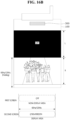
- the activated screen is a display area in examples of FIGS. 16A and 16B .
- the deactivated screen is a non-display area which displays black in the examples of FIGS. 16A and 16B .
- the gate driver may drive the gate lines at a frequency that is lower than that of the activated screen.
- a foldable display of the present disclosure includes a flexible display panel 100 and display panel drivers 120 and 300.
- the display panel drivers 120 and 300 include a gate driver 120 for supplying gate signals to gate lines GL1 and GL2 of the flexible display panel 100, a data driver 306 for converting pixel data into a voltage of a data signal and supplying the voltage to data lines through activated data output channels, and a timing controller 303 for activating data output channels of the data driver 306 according to a folding angle of the flexible display panel and controlling an operating timing of the data driver 306 and the gate driver 120.
- the data driver 306 and the timing controller 303 may be integrated in a drive integrated circuit (IC) 300.
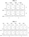
- a screen which reproduces an input image includes data lines DL1 to DL6, the gate lines GL1 and GL2 crossing the data lines DL1 to DL6, and a pixel array in which pixels P are disposed in the form of a matrix.
- the screen is at least divided into a first screen part L and a second screen part R.
- a folding boundary is present between the first screen part L and the second screen part R.
- the folding boundary may be a line along which the screen or the display panel is foldable.
- the flexible display panel 100 may include a plurality of folding boundaries A to be folded in various forms.
- the flexible display panel 100 may be folded with respect to the folding boundary as a boundary.
- the first screen part L, and the second screen part R (and optionally a screen part A adjacent to the folding boundary) are selectively driven according to a folded/unfolded state of the flexible display panel 100, a folding angle, or the like, and thus a size and a resolution of an activated screen displaying an image or information may be varied.
- the display panel driver in particular the timing controller 303, may determine a folded or unfolded state of the flexible display panel 100 on the basis of an enable signal EN from a host system 200 and further determine a folding angle of the flexible display panel 100.
- the display panel driver, in particular the timing controller 303 may control a size and a resolution of an activated screen in the unfolded state of the flexible display panel 100 as a maximum screen and a maximum resolution thereof.
- the first screen part L is substantially coplanar with the second screen part R.
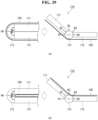
- the flexible display panel 100 may be folded in an in-folding method shown in FIG. 2A or an out-folding method shown in FIG. 2B .
- the in-folding method the first screen part L is brought into contact with the second screen part R inside the folded flexible display panel 100.
- the first screen part L and the second screen part R are disposed inside the folded flexible display panel 100, the first screen part L and the second screen part R are not exposed to the outside.
- the flexible display panel 100 is folded in the form in which the first screen part L and the second screen part R are back to back.
- the first screen part L and the second screen part R are both exposed to the outside.
- a resolution of one driven surface may be X*(Y+A/2). That is the width of the first screen part L and the second screen part R may correspond to Y+A/2.
- the first screen part L may be an upper half portion or a left half portion of the screen
- the second screen part R may be a lower half portion or a right half portion of the screen.
- the present invention is not limited to the first screen part L and the second screen part R being half of the entire screen, but the first screen part L and the second screen part R may also have different widths.
- the folding boundary may not be a center line, i.e. in the middle, of the entire screen. Also, there may be more than one folding boundary, and thus more screen parts than the first screen part L and the second screen part R.
- the screen part A adjacent to the folding boundary includes a portion of the screen part L and a portion of the screen part R, respectively adjacent to the folding boundary.
- An input image or information may also be displayed on pixels P of the screen part A adjacent to the folding boundary. Since the pixels P are disposed in the screen part A adjacent to the folding boundary, in the unfolded state in which the first screen part L and the second screen part R are unfolded, a portion in which an image is discontinued is not present between the first screen part L and the second screen part R.
- a width of the screen part A adjacent to the folding boundary that is, a length in a Y-axis, may be determined according to a curvature of the folding boundary A.
- a curvature of the screen part A adjacent to the folding boundary may be varied according to a folding angle of the flexible display panel 100.
- a resolution and a size of the screen part A adjacent to the folding boundary may be proportional to curvature of the folding boundary A. OFor example, the size of the folding boundary increases when the flexible display panel 100 is folded in half and becomes minimal when the flexible display panel 100 is unfolded as shown in FIG. 3 .
- X is an X-axis resolution of the entire screen constituted by the screen parts L, and R.
- Y+A+Y is a Y-axis resolution of the entire screen constituted by the screen parts L, and R.
- the pixel array when a resolution of a pixel array is n*m, the pixel array includes n pixel columns and m pixel lines crossing the n pixel columns.
- the pixel column includes pixels disposed in a Y-axis direction.
- the pixel line includes pixels disposed in an X-axis direction.
- One horizontal time 1H is a time obtained by dividing one frame interval by the m pixel lines.
- the drive IC 300 is connected to the host system 200, a first memory 301, and the flexible display panel 100. As shown in FIG. 6 , the drive IC 300 includes a data receiving and calculating part 308, the timing controller 303, and the data driver 306.
- the gate timing control signal (VST, CLK) output from the level shifter 307 is applied to the gate driver 120 to control the shift operation of the gate driver 120.
- GVST and GCLK shown in FIG. 6 are gate timing control signals applied to the first shift register 120G shown in FIG. 11 .
- EVST and ECLK illustrated in FIG. 6 are gate timing control signals applied to the second shift register 120E illustrated in FIG. 11 .
- the data receiving and calculating part 308 includes a receiver RX for receiving pixel data which is input as a digital signal from the host system 200, and a data calculator for processing the pixel data input through the receiver RX to improve image quality.
- the data calculator may include a data restoration part for decoding and restoring compressed pixel data and an optical compensator for adding a predetermined optical compensation value to the pixel data.
- the optical compensation value may be set to a value for correcting brightness of the pixel data on the basis of brightness of the screen measured based on a camera image which is captured in a manufacturing process.
- the data driver 306 converts the pixel data (a digital signal) received from the timing controller 303 into a gamma compensation voltage through a digital-to-analog converter (DAC) to provide voltages of data signals DATA1 to DATA6 (hereinafter referred to as "data voltages").
- the data voltages output from the data driver 306 are supplied to the data lines DL1 to DL6 of the pixel array through an output buffer (a source amplifier (AMP)) connected to data channels of the drive IC 300.
- a source amplifier AMP
- the level shifter 307 converts a low level voltage of the gate timing signal received from the timing controller 303 into the gate-on voltage VGL and converts a high level voltage of the gate timing signal into the gate-off voltage VGH.
- the level shifter 307 outputs the gate-off voltage VGH and the gate-on voltages VGL through the gate timing signal output channels and supplies the gate-off voltage VGH and the gate-on voltages VGL to the gate driver 120.
- the power supply 304 generates power required for driving the pixel array, the gate driver 120, and the drive IC 300 of the flexible display panel 100 using a direct current (DC)-DC converter.
- the DC-DC converter may include a charge pump, a regulator, a buck converter, and a boost converter.
- the power supply 304 may adjust a DC input voltage from the host system 200 to generate DC power such as a gamma reference voltage, the gate-on voltage VGL, the gate-off voltage VGH, a pixel driving voltage ELVDD, a low potential power voltage ELVSS, and an initialization voltage Vini.
- the gamma reference voltage is supplied to the gamma compensation voltage generator 305.
- the gate-on voltage VGL and the gate-off voltage VGH are supplied to the level shifter 307 and the gate driver 120.
- Pixel power such as the pixel driving voltage ELVDD, the low potential power voltage ELVSS, and the initialization voltage Vini, are commonly supplied to the pixels P.
- the drive element DT controls the current Ids flowing in the light emitting element OLED according to the gate-source voltage Vgs, thereby driving the light emitting element OLED.
- the drive element DT includes the gate connected to the second node n2, the first electrode connected to the first node n1, and the second electrode connected to the third node n3.
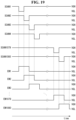
- the (N-1) th scan signal SCAN(N-1) is generated as the gate-on voltage VGL.
- the N th scan signal SCAN(N) and the EM signal EM(N) are maintained as the gate-off voltage VGH.
- the fifth and sixth switching elements M5 and M6 are turned on so that the second and fourth nodes n2 and n4 are initialized at Vini.
- a hold time Th may be set between the initialization time Tini and the sampling time Tsam.
- a voltage level of the gate signals SCAN(N-1), SCAN(N), and EM(N) are the gate-off voltage VGH.
- a gate voltage DTG of the drive element DT rises due to a current flowing through the first and second switching elements M1 and M2. Since the drive element DT is turned off when the drive element DT is turned off, the gate node voltage DTG is Vdata-
- the gate-source voltage Vgs of the drive element DT satisfies
- Vdata-(Vdata-
- )
- the EM signal EM(N) may be generated at the gate-off voltage VGH.
- the EM signal EM(N) may be turned on or off at a predetermined duty ratio to swing between the gate-on voltage VGL and the gate-off voltage VGH. Accordingly, the EM signal EM(N) may be generated at the gate-on voltage VGL for at least a part of the light emission time Tem.
- the EM signal EM(N) When the EM signal EM(N) is the gate-on voltage VGL, a current flows between an ELVDD and the light emitting element OLED so that the light emitting element OLED may emit light.
- the (N-1) th and N th scan signals SCAN(N-1) and SCAN(N) are maintained as the gate-off voltage VGH.
- the third and fourth switching elements M3 and M4 are repeatedly turned on and off according to a voltage of the EM signal EM(N).
- the third and fourth switching elements M3 and M4 When the EM signal EM(N) is the gate-on voltage VGL, the third and fourth switching elements M3 and M4 are turned on so that a current flows in the light emitting element OLED.
- Vgs of the drive element DT satisfies
- ELVDD-(Vdata-
- K is a proportional constant determined by charge mobility, parasitic capacitance, and a channel capacity of the drive element DT.
- the gates of the fifth and sixth switching elements M5 and M6 may be connected to the different gate lines 32a and 32b.
- a control signal of the sixth switch element M6 may be different in the activated screen from the deactivated screen.
- the (N-1) th scan signal SCAN(N-1) is applied to the gate of the sixth switching element M6.
- the N th scan signal SCAN(N) is applied to the gate of the sixth switching element M6.
- the (N-1) th scan signal SCAN(N-1) is applied to the gates of the fifth and sixth switching elements M5 and M6.
- the (N-1) th scan signal SCAN(N-1) is applied to the gate of the fifth switch element M5 and then the N th scan signal SCAN(N) is applied to the sixth switch element M6.
- the sixth switching element M6 reduces an anode voltage of the light emitting element OLED to Vini, thereby suppressing light emission of the light emitting element OLED. Consequently, the pixels of the deactivated screen maintain brightness of a black gray scale due to not emitting light.
- brightness of the deactivated screen may be controlled to the brightness of the black gray scale only by turning the sixth switch element M6 on during the sampling time Tsam and applying Vini to the anode of the light emitting element OLED. In this case, as shown in FIG. 18 , in order to block an influence of other nodes connected to the anode of the light emitting element OLED, it is preferable that the third switching element M3 and the fourth switching element M4 are turned off.
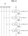
- FIG. 8 is a schematic diagram illustrating a circuit configuration of a shift register in the gate driver 120.
- FIGS. 9A and 9B are schematic diagrams illustrating a pass-gate circuit and an edge trigger circuit.
- the shift register of the gate driver 120 includes stages ST(n-1) to ST(n+2) which are connected in cascade.
- the shift register receives the gate start pulse VST or carry signals CAR1 to CAR4 received from previous stages as the gate start pulse VST and generates output signals Gout(n-1) to Gout(n+2) in synchronization with rising edges of gate shift clocks CLK1 to CLK4.
- the output signals of the shift register include the gate signals SCAN(N-1), SCAN(N), and EM(N).
- the stages ST(n-1) to ST(n + 2) of the shift register may be implemented as pass-gate circuits as shown in FIG. 9A and/or edge trigger circuits as shown in FIG. 9B .
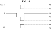
- a clock CLK is input to a pull-up transistor Tup which is turned on or off according to a voltage of a node Q.
- the gate-on voltage VGL is supplied to a pull-up transistor Tup of the edge trigger circuit, and the gate start pulse VST and the gate shift clocks CLK1 to CLK4 are input to the edge trigger circuit.
- a pull-down transistor Tdn is turned on or off according to a voltage of a node QB.
- the node Q is floated according to a start signal in a pre-charged state.
- the edge trigger circuit Since the voltage of the output signal Gout(n) is changed to a voltage of the start signal in synchronization with the edge of the clock CLK, the edge trigger circuit generates the output signal Gout(n) in the same waveform as a phase of the start signal. When a waveform of the start signal is changed, the waveform of the output signal is changed accordingly.
- an input signal may overlap the output signal.
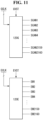
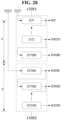
- FIG. 11 is a diagram illustrating a first shift register and a second shift register of the gate driver 120.
- the first and/or the second shift register may be as illustrated in Fig. 8 .
- the gate driver 120 may include a first shift register 120G and a second shift register 120E.
- the first shift register 120G may receive a gate start pulse GVST and a gate shift clock GCLK and sequentially output scan signals SCAN1 to SCAN2160.
- the second shift register 120E may receive a gate start pulse EVST and a gate shift clock ECLK and sequentially output EM signals EM1 to EM2160.
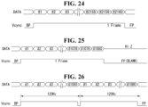
- FIG. 12 is a detailed diagram illustrating an active interval and a vertical blank interval of one frame interval.
- pixel data of one frame which will be written in all the pixels P on the screen parts L, A, and R of the display panel 100, is received by the drive IC 300 and written in the pixels P.
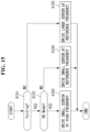
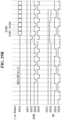
- FIGS. 29A and 29B are waveform diagrams illustrating a data signal and a gate start pulse when only some of the screen parts are activated.
- GCLK1 and GCLK2 represent the gate shift clocks input to the first-first shift register 120G1 and the first-second shift register 120G2.
- ECLK1 and ECLK2 represent the gate shift clocks input to the second-first shift register 120E1 and the second-second shift register 120E2.
- the gate driving frequency of the deactivated screen is decreased to half or less compared to the gate driving frequency of the activated screen.
- the gate driving frequency means the frequency of the gate start pulse or the frame frequency.
- the gate driving frequency of the second screen part R is decreased to half or less compared to the gate driving frequency of the first screen part L.
- the gate driving frequency of the first screen part L is decreased to half or less compared to the gate driving frequency of the second screen part R. Therefore, according to the present disclosure, when the screen of the foldable display is partially driven, power consumption of the gate driver 120 may be significantly reduced.
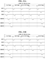
- FIGS. 30A to 31B are waveform diagrams illustrating a control method of a gate driving frequency in a folded state of the foldable display according to an embodiment of the present disclosure.
- the first screen part L displays an image
- the second screen part R displays black.
- GVST1 and EVST1 are start pulses applied to the gate driver that drives the gate lines of the activated screen.
- GVST2 and EVST2 are start pulses applied to the gate driver that drives the gate lines of the deactivated screen.
- SCAN1 to SCAN1080 are scan pulses of the activated screen that are shifted in response to GVST1.
- SCAN1081 to SCAN2160 are scan pulses of the deactivated screen that are shifted in response to GVST2.
- the first gate driver 120G1 and 120E1 sequentially outputs the scan signals SCAN1 to SCAN1080 by receiving the first gate start pulses GVST1 and EVST1, which are generated at a frame frequency of 60 Hz, and the gate shift clocks.
- the second gate driver 120G2 and 120E2 sequentially outputs the scan signals SCAN1081 to SCAN2160 by receiving the second gate start pulses GVST2 and EVST2, which are generated at a frame frequency of 30 Hz, and the gate shift clocks.
- the first and second gate drivers 120G1 and 120G2 sequentially output the scan pulses SCAN1 to SCAN2160 in response to the gate start pulses GVST1 and GVST2.
- the scan pulses SCAN1 to SCAN1080 applied to the gate lines of the first screen part L are synchronized with the data voltage Vdata of the pixel data. Since the data voltage Vdata is not generated during the scanning time of the second screen part R, the scan pulses SCAN1 to SCAN1080 applied to the gate lines of the second screen part R are not synchronized with the data voltage Vdata and turn the switch element M6 on as shown in FIG. 18 .
- the second gate driver 120G2 does not output the scan pulse. In this case, since the second gate driver 120G2 is not driven, power consumption does not occur.
- the pixel data is written to the pixels of the first screen part L again so that an input image of the even-numbered frames is displayed.
- the pixels of the second screen part R hold the black gray scale.
- the first-second start pulse GVST2 and the second-second start pulse EVST2 may not be input to the second gate driver 120G.
- the first gate driver 120G1 and 120E1 sequentially outputs the scan signals SCAN1 to SCAN1080 by receiving the first gate start pulses GVST1 and EVST1, which are generated at a frame frequency of 60 Hz, and the gate shift clocks.
- the second gate driver 120G2 and 120E2 sequentially outputs the scan signals SCAN1081 to SCAN2160 by receiving the second gate start pulses GVST2 and EVST2, which are generated at a frame frequency of 60/n Hz (n is a positive integer ranging from 2 and 60), and the gate shift clocks.
- n is a positive integer ranging from 2 and 60
- the second gate driver 120G2 and 120E2 receives the second gate start pulses GVST2 and EVST2 generated at a frame frequency of 1 Hz.
- the first and second gate driver 120G1 and 120G2 sequentially outputs the scan pulses SCAN1 to SCAN2160 in response to the gate start pulses GVST1 and GVST2.
- the scan pulses SCAN1 to SCAN1080 applied to the gate lines of the first screen part L are synchronized with the data voltage Vdata of the pixel data. Since the data voltage Vdata is not generated during the scanning time of the second screen part R, the scan pulses SCAN1 to SCAN1080 applied to the gate lines of the second screen part R are not synchronized with the data voltage Vdata and turn the switch element M6 on as shown in FIG. 18 .
- the input image of the odd-numbered frames is displayed on the pixels of the first screen part L.
- Vini is applied to the anodes of the light emitting elements OLED so that the pixels of the second screen part R display the black gray scale.
- the EM signal EM(N) may be maintained as the gate-off voltage VGH.
- the gate start pulses GVST1, GVST2, EVST1, and EVST2 may be input to the first and second gate drivers 120G1 and 120G2.
- the scan pulses SCAN1 to SCAN2160 and the pulses of the EM signals may be sequentially output to the first and second screen parts L and R.
- the first gate driver 120G1 sequentially outputs the scan pulses SCAN1 to SCAN1080 in response to the gate start pulse GVST1.
- the scan pulses SCAN1 to SCAN1080 applied to the gate lines of the first screen part L are synchronized with the data voltage Vdata of the pixel data.
- the second gate driver 120G2 since the first-second start pulse GVST2 is not input to the second gate driver 120G2, the second gate driver 120G2 does not output the scan pulse. In this case, since the second gate driver 120G2 is not driven, power consumption does not occur.
- the ELVSS variable device selects the register setting value REG in response to the enable signal EN or the frequency detection signal FREQ. For example, the ELVSS variable device reduces the voltage of the ELVSS to decrease a rate of change in brightness of the pixels when the gate driving frequency is reduced.
- the ELVSS variable device may output ELVSS having a different voltage for each frequency according to the register setting value REG.
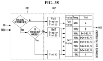
- the power supply 304 of the drive IC 300 may include a Vini variable device.
- the Vini variable device includes a determiner 361, a Vini setting part 362, and a Vini generator 363.
- the determiner 361 determines whether the foldable display is folded and determines the gate driving frequency or the frame frequency in response to the enable signal EN or the frequency detection signal FREQ.
- the determiner 361 may determine a folded state or an unfolded state of the foldable display according to the enable signal EN.
- the determiner 361 may determine the gate driving frequency or the frame frequency according to the frequency detection signal FREQ.
- the Vini setting part 362 receives a folding and frequency determination signal from the determiner 321.
- the Vini setting part 362 outputs a register setting value REG in response to the folding and frequency determination signal.
- Vini is decreased in the folded state in which the IR drop amount is small, and the brightness of the pixels is decreased so that the decreased brightness of the pixels is made to be equal to the brightness in the unfolded state.
- a voltage of the capacitor Cst does not reach a target level of the data voltage Vdata within a fixed sampling time Tsam, and thus a charging rate of the capacitor Cst is decreased.
- a difference in IR drop amount between the folded state and the unfolded is compensated for with Vini so that a change in brightness of the screen may be minimized regardless of whether the foldable display is folded.
- the Vini setting part 362 selects a register setting value REG to compensate for the difference in IR drop amount in the unfolded state and the folded state in response to the folding and frequency determination signal.
- the Vini setting part 362 selects the register setting value REG as A in the unfolded state of the foldable display. Meanwhile, in order to decrease the voltage level of Vini to decrease the brightness of the pixels in the unfolded state of the foldable display, the Vini setting part 362 selects the register setting value REG as B.
- A may be set to a value that is greater than B (A>B).
- the Vini variable device compensates for a decrease in brightness of pixels, which is caused when the gate driving frequency or the frame frequency of the deactivated screen in the folded state is decreased, by varying the voltage of Vini.
- Vini supplied to the pixels of the deactivated screen may be set to a voltage that is higher than Vini supplied to the pixels of the activated screen.
- Vini applied to the anode of the light emitting element OLED decreases brightness of a black gray scale of the pixels in the deactivated screen.
- the gate driving frequency of the deactivated screen is decreased, the voltage of the capacitor Cst in the pixels is decreased so that the rate of change in brightness of the pixels is increased.
- Vini applied to the anode of the light emitting element OLED in the deactivated screen is varied according to the gate driving frequency.
- the decrease in brightness of pixels which is decreased as the frequency is decreased when the foldable display is folded, is compensated for by increasing the voltage level of Vini.
- a voltage of the anode of the light emitting element OLED is increased so that the brightness of the pixel is increased.
- the Vini setting part 362 varies the register setting value REG for each frequency so as to adaptively vary the voltage level of Vini according to the gate driving frequency in the folded state of the foldable display in response to the folding and frequency determination signal.
- the DC-DC converter of the power supply 304 may vary an output voltage level according to the resistor setting value REG.
- the register setting value REG is differently set for each frequency. For example, as in an example of FIG. 38 , 5 Hz of the deactivated screen may be set to C, and 60 Hz of the deactivated screen may be set to A. When the foldable display is unfolded, 60 Hz may be set to A.
- the Vini generator 363 may determine a duty ratio of a PWM signal to vary the voltage level of Vini in response to the register setting value REG from the Vini setting part 362.
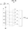
- the reference voltage generator 40 divides a high potential reference voltage VDD and a ground voltage source GND and outputs a plurality of reference voltages having different voltage levels through voltage dividing nodes using a voltage divider circuit including resistors R01 ⁇ R04 connected in series.
- Each of the comparators 411 to 415 compares a reference voltage from the reference voltage generator 40 with the folding voltage Vout, outputs a high voltage when the folding voltage Vout is higher than the reference voltage, and outputs a low voltage when the folding voltage Vout is lower than or equal to the reference voltage.
- the first comparator 411 compares a highest level reference voltage with a folding voltage Vout and outputs a highest voltage when the folding voltage Vout is higher than the highest level reference voltage, otherwise, the first comparator 411 outputs a low voltage.
- the fifth comparator 415 compares a lowest level reference voltage with the folding voltage Vout and outputs the high voltage when the folding voltage Vout is higher than the lowest level reference voltage, otherwise, the fifth comparator 415 outputs the low voltage.
Landscapes
- Engineering & Computer Science (AREA)
- Theoretical Computer Science (AREA)
- Physics & Mathematics (AREA)
- General Physics & Mathematics (AREA)
- Computer Hardware Design (AREA)
- Control Of Indicators Other Than Cathode Ray Tubes (AREA)
- Electroluminescent Light Sources (AREA)
- General Engineering & Computer Science (AREA)
Claims (5)
- Anzeigevorrichtung, die umfasst:eine Anzeigetafel (100), die einen Bildschirm mit mehreren Pixeln, Gate-Leitungen und Datenleitungen enthält, wobei die Anzeigetafel (100) entlang einer vordefinierten Faltgrenze (A) faltbar ist, um den Bildschirm in einen vordefinierten ersten Bildschirmteil (L) und einen vordefinierten zweiten Bildschirmteil (R) zu falten, wobei jedes der Pixel enthält: eine lichtemittierende Diode (OLED); ein Ansteuerungselement (DT), das zwischen einem Pixelansteuerungsspannungsanschluss (ELVDD) und der lichtemittierenden Diode (OLED) angeordnet ist, um an die lichtemittierende Diode Strom zu liefern; und einen Kondensator (Cst), der mit dem Pixelansteuerungsspannungsanschluss (ELVDD) und mit einem Gate des Ansteuerungselements (DT) verbunden ist;eine erste Gate-Ansteuerungseinrichtung (120G1, 120E1), die mit mehreren Gate-Leitungen auf dem ersten Bildschirmteil (L) verbunden ist und konfiguriert ist, in Reaktion auf einen ersten Gate-Startimpuls (GVST1, EVST1) Gate-Signale an die Gate-Leitungen auf dem ersten Bildschirmteil (L) zu liefern;eine zweite Gate-Ansteuerungseinrichtung (120G2, 120E), die mit mehreren Gate-Leitungen auf dem zweiten Bildschirmteil (R) verbunden ist und konfiguriert ist, in Reaktion auf einen zweiten Gate-Startimpuls (GVST2, EVST2) Gate-Signale an die Gate-Leitungen auf dem zweiten Bildschirmteil (R) zu liefern;eine Datenansteuerungseinrichtung (306), die mit mehreren Datenleitungen (102) auf dem ersten und dem zweiten Bildschirmteil (L, R) verbunden ist und konfiguriert ist, eine Datenspannung (Vdata) eines Bildes, das in Datenleitungen (102) eingegeben wird, zu liefern; undeine Anzeigetafel-Ansteuerungseinrichtung (120, 300), die konfiguriert ist, den ersten Gate-Startimpuls (GVST1, EVST1) und den zweiten Gate-Startimpuls (GVST2, EVST2) zu erzeugen,wobei in einem gefalteten Zustand der Anzeigetafel (100)die Anzeigetafel-Ansteuerungseinrichtung (120, 300) konfiguriert ist, einen des ersten und des zweiten Bildschirmteils (L, R) zu aktivieren, um ein Bild auf dem aktivierten Bildschirmteil (L, R) anzuzeigen, und den anderen des ersten und des zweiten Bildschirmteils (L, R) zu deaktivieren und eine Schwarz-Grau-Skala auf dem deaktivierten Bildschirmteil anzuzeigen,eine erste Gate-Ansteuerungseinrichtung (120G1, 120E) konfiguriert ist, Gate-Signale in der Form von Abtastimpulsen an Gate-Leitungen des aktivierten oder deaktivierten ersten Bildschirmteils anhand des ersten Gate-Startimpulses (GVST1, EVST1) zu liefern,die zweite Gate-Ansteuerungseinrichtung (120G2, 120E2) konfiguriert ist, Gate-Signale in der Form von Abtastimpulsen an Gate-Leitungen des deaktivierten oder aktivierten zweiten Bildschirmteils anhand des zweiten Gate-Startimpulses zu liefern,wobei dann, wenn der erste Bildschirmteil (L) aktiviert ist und der zweite Bildschirmteil (R) deaktiviert ist, die erste Gate-Ansteuerungseinrichtung (120G1, 120E1) konfiguriert ist, die Gate-Signale durch Empfangen des ersten Gate-Startimpulses (GVST1, EVST1), der mit einer Rahmenfrequenz von 60 Hz erzeugt wird, und von Gate-Verschiebungstakten auszugeben, und die zweite Gate-Ansteuerungseinrichtung (120G2, 120E2) konfiguriert ist, die Gate-Signale durch Empfangen des zweiten Gate-Startimpulses (GVST2, EVST2), der mit einer Rahmenfrequenz von 60/n Hz erzeugt wird, und von Gate-Verschiebungstakten auszugeben, wobei n eine positive ganze Zahl ist, die in einem Bereich von 2 bis 60 liegt.
- Anzeigevorrichtung nach Anspruch 1, wobei das Ansteuerungselement (DT) eine erste Elektrode, die mit einem ersten Knoten (n1) verbunden ist, das Gate, das mit einem zweiten Knoten (n2) verbunden ist, und eine zweite Elektrode, die mit einem dritten Knoten (n3) verbunden ist, enthält,
wobei jedes der Pixel enthält:ein erstes Schaltelement (M1), das konfiguriert ist, in Reaktion auf einen Gate-Einschaltspannungsimpuls eines N-ten Abtastsignals eingeschaltet zu werden, wobei N eine natürliche Zahl ist, um den zweiten Knoten (n2) mit dem dritten Knoten (n3) zu verbinden;ein zweites Schaltelement (M2), das konfiguriert ist, in Reaktion auf den Gate-Einschaltspannungsimpuls des N-ten Abtastsignals eingeschaltet zu werden, um eine Datenleitung (102) mit dem ersten Knoten (n1) zu verbinden;ein drittes Schaltelement (M3), das konfiguriert ist, in Reaktion auf eine Gate-Einschaltspannung des Lichtemissionssteuersignals eingeschaltet zu werden, um den Pixelansteuerungsspannungsanschluss (ELVDD) mit dem ersten Knoten (n1) zu verbinden;ein viertes Schaltelement (M4), das konfiguriert ist, in Reaktion auf die Gate-Einschaltspannung des Lichtemissionssteuersignals eingeschaltet zu werden, um die zweite Elektrode des Ansteuerungselements (DT) mit der Anode der lichtemittierenden Diode (OLED) zu verbinden;ein fünftes Schaltelement (M5), das konfiguriert ist, in Reaktion auf eine Gate-Einschaltspannung eines (N-1)-ten Abtastsignals eingeschaltet zu werden, um den zweiten Knoten (n2) mit einer Stromleitung (105) zu verbinden, an die eine Initialisierungsspannung (Vini) geliefert wird; undein sechstes Schaltelement (M6), das konfiguriert ist, in Reaktion auf eine Gate-Einschaltspannung des (N-1)-ten oder des N-ten Abtastsignals eingeschaltet zu werden, um die Stromleitung (105) mit der Anode der lichtemittierenden Diode (OLED) zu verbinden. - Verfahren zum Ansteuern einer Anzeigevorrichtung nach Anspruch 1, wobei das Verfahren umfasst:in einem gefalteten Zustand der Anzeigetafel (100)Liefern von Gate-Signalen in der Form von Abtastimpulsen an Gate-Leitungen eines des ersten Bildschirmteils (L) und des zweiten Bildschirmteils (R), um diesen zum Anzeigen eines Bildes auf einem aktivierten Bildschirmteil zu aktivieren, und Liefern von Gate-Signalen in der Form von Abtastimpulsen an Gate-Leitungen des anderen des ersten und des zweiten Bildschirmteils (L, R), um denselben zu deaktivieren und eine Schwarz-Grau-Skala auf dem deaktivierten Bildschirmteil anzuzeigen,wobei dann, wenn der erste Bildschirmteil (L) aktiviert ist und der zweite Bildschirmteil (R) deaktiviert ist, die erste Gate-Ansteuerungseinrichtung (120G1, 120E1) die Gate-Signale durch Empfangen des ersten Gate-Startimpulses (GVST1, EVST1), der mit einer Rahmenfrequenz von 60 Hz erzeugt wird, und von Gate-Verschiebungstakten ausgibt und die zweite Gate-Ansteuerungseinrichtung (120G2, 120E2) die Gate-Signale durch Empfangen des zweiten Gate-Startimpulses (GVST2, EVST2), der mit einer Rahmenfrequenz von 60/n Hz erzeugt wird, und von Gate-Verschiebungstakten ausgibt, wobei n eine positive ganze Zahl ist, die in einem Bereich von 2 bis 60 liegt.
- Verfahren nach Anspruch 3, wobei das Gate-Signal enthält:ein N-tes Abtastsignal (SCAN), das mit der Datenspannung (Vdata) des Bildes, das in den aktivierten Bildschirmteil eingegeben wird, synchronisiert ist, wobei in dem deaktivierten Bildschirmteil das N-te Abtastsignal ein Schaltelement (M6), das mit einer Anode der lichtemittierenden Diode (OLED) verbunden ist, steuert, eine Initialisierungsspannung (Vini) zum Unterdrücken einer Lichtemission der lichtemittierenden Diode zu liefern; undein N-tes Lichtemissionssteuersignal (EM), das einen Stromweg der lichtemittierenden Diode schaltet.
- Verfahren nach Anspruch 4, wobei:eine Ansteuerungszeit jedes der Pixel in eine Initialisierungszeit (Tini), eine Abtastzeit (Tsam), eine Datenschreibzeit (Twr) und eine Lichtemissionszeit (Tem) unterteilt ist;während der Initialisierungszeit das (N-1)-te Abtastsignal als ein Impuls der Gate-Einschaltspannung erzeugt wird und eine Spannung jedes des N-ten Abtastsignals und des Lichtemissionssteuersignals als die Gate-Ausschaltspannung erzeugt wird;während der Abtastzeit das N-te Abtastsignal als der Impuls der Gate-Einschaltspannung erzeugt wird und eine Spannung jedes des (N-1)-ten Abtastsignals und des Lichtemissionssteuersignals als die Gate-Ausschaltspannung erzeugt wird;während der Datenschreibzeit eine Spannung jedes des (N-1)-ten Abtastsignals, des N-ten Abtastsignals und des Lichtemissionssteuersignals als die Gate-Ausschaltspannung erzeugt wird; undwährend zumindest einiger Zeit der Lichtemissionszeit das Lichtemissionssteuersignal als die Gate-Einschaltspannung erzeugt wird und die Spannung jedes des (N-1)-ten Abtastsignals und des N-ten Abtastsignals als die Gate-Ausschaltspannung erzeugt wird.
Applications Claiming Priority (1)
| Application Number | Priority Date | Filing Date | Title |
|---|---|---|---|
| KR1020190067021A KR102631015B1 (ko) | 2019-06-05 | 2019-06-05 | 폴더블 디스플레이와 그 구동 방법 |
Publications (2)
| Publication Number | Publication Date |
|---|---|
| EP3748623A1 EP3748623A1 (de) | 2020-12-09 |
| EP3748623B1 true EP3748623B1 (de) | 2025-07-02 |
Family
ID=70921814
Family Applications (1)
| Application Number | Title | Priority Date | Filing Date |
|---|---|---|---|
| EP20177221.7A Active EP3748623B1 (de) | 2019-06-05 | 2020-05-28 | Anzeigevorrichtung und verfahren zur steuerung davon |
Country Status (5)
| Country | Link |
|---|---|
| US (1) | US11217178B2 (de) |
| EP (1) | EP3748623B1 (de) |
| KR (1) | KR102631015B1 (de) |
| CN (1) | CN112053660B (de) |
| TW (1) | TWI739462B (de) |
Families Citing this family (31)
| Publication number | Priority date | Publication date | Assignee | Title |
|---|---|---|---|---|
| CN111028753B (zh) * | 2019-12-06 | 2023-06-27 | Tcl华星光电技术有限公司 | 数据驱动延迟补偿装置及其方法、显示装置 |
| KR102715638B1 (ko) * | 2019-12-20 | 2024-10-14 | 삼성디스플레이 주식회사 | 표시 장치 |
| KR102766490B1 (ko) * | 2020-06-26 | 2025-02-13 | 삼성디스플레이 주식회사 | 표시 장치 및 이의 구동 방법 |
| KR102775867B1 (ko) * | 2020-06-29 | 2025-03-07 | 삼성디스플레이 주식회사 | 표시 장치 |
| KR102812492B1 (ko) | 2020-09-08 | 2025-05-27 | 삼성디스플레이 주식회사 | 표시 장치 및 그것의 구동 방법 |
| KR102760435B1 (ko) * | 2020-11-03 | 2025-02-04 | 삼성디스플레이 주식회사 | 표시장치 |
| KR102745198B1 (ko) * | 2020-12-28 | 2024-12-20 | 삼성전자주식회사 | 휘도 보상기 및 이를 포함하는 디스플레이 시스템 |
| CN112735313B (zh) * | 2020-12-30 | 2022-12-06 | 武汉华星光电半导体显示技术有限公司 | 显示面板及电子设备 |
| KR102454533B1 (ko) * | 2021-01-12 | 2022-10-14 | 연세대학교 산학협력단 | 스트레처블 디스플레이 구동 장치 |
| KR102880839B1 (ko) * | 2021-02-09 | 2025-11-05 | 삼성전자 주식회사 | 디스플레이의 잔상을 줄일 수 있는 전자 장치 및 방법 |
| WO2022173166A1 (ko) | 2021-02-09 | 2022-08-18 | 삼성전자 주식회사 | 디스플레이의 잔상을 줄일 수 있는 전자 장치 및 방법 |
| KR102843304B1 (ko) * | 2021-05-07 | 2025-08-07 | 삼성디스플레이 주식회사 | 표시 장치 |
| TWI828189B (zh) | 2021-07-08 | 2024-01-01 | 南韓商Lg顯示器股份有限公司 | 像素電路及包含該像素電路的顯示裝置 |
| KR102910454B1 (ko) * | 2021-07-26 | 2026-01-12 | 삼성디스플레이 주식회사 | 표시 장치 및 그것의 구동 방법 |
| CN115708147A (zh) * | 2021-08-18 | 2023-02-21 | 深圳市柔宇科技股份有限公司 | 一种折叠屏幕亮度差异改善方法、电子设备及存储介质 |
| CN115729368A (zh) * | 2021-08-31 | 2023-03-03 | 联咏科技股份有限公司 | 时序控制电路及时序控制方法 |
| US12379808B2 (en) | 2021-08-31 | 2025-08-05 | Novatek Microelectronics Corp. | Timing control circuit and timing control method thereof |
| KR102894671B1 (ko) | 2021-10-05 | 2025-12-04 | 삼성디스플레이 주식회사 | 표시 장치 |
| KR102896296B1 (ko) * | 2021-12-29 | 2025-12-08 | 엘지디스플레이 주식회사 | 표시장치 |
| KR20230118211A (ko) * | 2022-02-03 | 2023-08-11 | 삼성디스플레이 주식회사 | 표시 장치 및 표시 장치의 구동 방법 |
| WO2023159544A1 (zh) * | 2022-02-28 | 2023-08-31 | 京东方科技集团股份有限公司 | 数据驱动方法、源极驱动器和显示装置 |
| WO2024000279A1 (zh) | 2022-06-29 | 2024-01-04 | 京东方科技集团股份有限公司 | 显示面板及其显示方法、显示装置 |
| KR102950127B1 (ko) * | 2022-06-30 | 2026-04-10 | 삼성디스플레이 주식회사 | 표시 장치 및 그것의 구동 방법 |
| WO2024019295A1 (ko) * | 2022-07-18 | 2024-01-25 | 삼성전자주식회사 | 전원 공급 방법 및 상기 방법을 수행하는 전자 장치 |
| CN115188325B (zh) * | 2022-08-08 | 2025-08-22 | 上海天马微电子有限公司 | 一种显示面板及显示装置 |
| CN118248038B (zh) | 2022-12-23 | 2025-02-07 | 荣耀终端有限公司 | 一种折叠屏的显示方法及电子设备 |
| KR20240107989A (ko) * | 2022-12-30 | 2024-07-09 | 엘지디스플레이 주식회사 | 표시 장치 |
| CN119600904A (zh) * | 2023-09-04 | 2025-03-11 | 荣耀终端股份有限公司 | 控制方法、存储介质及电子设备 |
| CN119252177B (zh) * | 2024-03-22 | 2025-12-30 | 荣耀终端股份有限公司 | 折叠屏、显示系统、电子设备以及屏幕亮度控制方法 |
| WO2026005312A1 (ko) * | 2024-06-25 | 2026-01-02 | 삼성전자주식회사 | 표시 영역을 가지는 디스플레이를 포함하는 전자 장치 |
| CN120980162B (zh) * | 2025-10-21 | 2025-12-23 | 四川酷赛科技有限公司 | 一种折叠屏手机的可靠性测试方法及系统 |
Citations (1)
| Publication number | Priority date | Publication date | Assignee | Title |
|---|---|---|---|---|
| EP3113012A2 (de) * | 2015-06-30 | 2017-01-04 | LG Display Co., Ltd. | Anzeigevorrichtung und mobiles endgerät damit |
Family Cites Families (16)
| Publication number | Priority date | Publication date | Assignee | Title |
|---|---|---|---|---|
| JP3744826B2 (ja) * | 2001-06-04 | 2006-02-15 | セイコーエプソン株式会社 | 表示制御回路、電気光学装置、表示装置及び表示制御方法 |
| WO2011058885A1 (en) * | 2009-11-13 | 2011-05-19 | Semiconductor Energy Laboratory Co., Ltd. | Display device and electronic device including the same |
| JP2013225052A (ja) | 2012-04-23 | 2013-10-31 | Sony Corp | 表示装置 |
| KR102061108B1 (ko) * | 2013-01-16 | 2020-01-02 | 삼성디스플레이 주식회사 | 터치 스크린 패널 일체형 유기전계 발광 표시장치 |
| KR102050380B1 (ko) | 2013-04-30 | 2019-11-29 | 엘지디스플레이 주식회사 | 저속 구동용 표시장치와 그 구동방법 |
| TWI667644B (zh) * | 2013-07-19 | 2019-08-01 | 日商半導體能源研究所股份有限公司 | 資料處理裝置 |
| CN105452981B (zh) | 2013-08-02 | 2021-08-24 | 株式会社半导体能源研究所 | 显示装置 |
| TWI533273B (zh) * | 2014-10-24 | 2016-05-11 | 友達光電股份有限公司 | 電力管理方法與電力管理裝置 |
| US9947269B2 (en) * | 2015-05-28 | 2018-04-17 | Lg Display Co., Ltd. | Organic light emitting display and circuit thereof |
| CN106057855B (zh) * | 2016-05-30 | 2019-02-19 | 武汉华星光电技术有限公司 | 可折叠显示装置及其驱动方法 |
| KR102603440B1 (ko) * | 2016-10-10 | 2023-11-20 | 삼성디스플레이 주식회사 | 폴더블 표시 장치 |
| KR102662906B1 (ko) * | 2017-02-13 | 2024-05-08 | 삼성디스플레이 주식회사 | 표시 장치 및 그의 구동 방법 |
| KR102309599B1 (ko) * | 2017-04-11 | 2021-10-08 | 삼성디스플레이 주식회사 | 유기전계발광 표시장치 |
| KR102421673B1 (ko) | 2017-05-26 | 2022-07-19 | 삼성디스플레이 주식회사 | 디스플레이 장치 및 그의 구동 방법 |
| KR102419041B1 (ko) | 2017-12-06 | 2022-07-11 | 현대자동차주식회사 | 자동차 실내 조명에 따른 사용자기기 조명제어 시스템 및 그 방법 |
| CN109584806B (zh) | 2019-02-01 | 2020-08-28 | 武汉天马微电子有限公司 | 一种显示面板及其驱动方法和显示装置 |
-
2019
- 2019-06-05 KR KR1020190067021A patent/KR102631015B1/ko active Active
-
2020
- 2020-05-28 EP EP20177221.7A patent/EP3748623B1/de active Active
- 2020-06-02 US US16/890,521 patent/US11217178B2/en active Active
- 2020-06-04 CN CN202010500184.3A patent/CN112053660B/zh active Active
- 2020-06-05 TW TW109119014A patent/TWI739462B/zh active
Patent Citations (1)
| Publication number | Priority date | Publication date | Assignee | Title |
|---|---|---|---|---|
| EP3113012A2 (de) * | 2015-06-30 | 2017-01-04 | LG Display Co., Ltd. | Anzeigevorrichtung und mobiles endgerät damit |
Also Published As
| Publication number | Publication date |
|---|---|
| KR102631015B1 (ko) | 2024-01-30 |
| TW202046281A (zh) | 2020-12-16 |
| US20200388228A1 (en) | 2020-12-10 |
| CN112053660B (zh) | 2022-10-25 |
| KR20200140152A (ko) | 2020-12-15 |
| CN112053660A (zh) | 2020-12-08 |
| EP3748623A1 (de) | 2020-12-09 |
| US11217178B2 (en) | 2022-01-04 |
| TWI739462B (zh) | 2021-09-11 |
Similar Documents
| Publication | Publication Date | Title |
|---|---|---|
| EP3748623B1 (de) | Anzeigevorrichtung und verfahren zur steuerung davon | |
| US11100900B2 (en) | Foldable display and driving method thereof | |
| US11341933B2 (en) | Foldable display and driving method thereof | |
| US11462171B2 (en) | Gate driving circuit and flexible display using the same | |
| KR102611008B1 (ko) | 표시장치와 그 구동 방법 | |
| CN114550658B (zh) | 显示装置及其驱动方法 | |
| KR102720345B1 (ko) | 게이트 구동회로 및 이를 이용한 플렉시블 디스플레이 | |
| US12505806B2 (en) | Gate driving circuit | |
| KR20220032767A (ko) | 게이트 구동 장치와 이를 이용한 표시장치 | |
| US12380859B2 (en) | Gate driver, display device including the same, and driving method of display device | |
| US20250218390A1 (en) | Gate driver and display device including the same |
Legal Events
| Date | Code | Title | Description |
|---|---|---|---|
| PUAI | Public reference made under article 153(3) epc to a published international application that has entered the european phase |
Free format text: ORIGINAL CODE: 0009012 |
|
| STAA | Information on the status of an ep patent application or granted ep patent |
Free format text: STATUS: REQUEST FOR EXAMINATION WAS MADE |
|
| 17P | Request for examination filed |
Effective date: 20200528 |
|
| AK | Designated contracting states |
Kind code of ref document: A1 Designated state(s): AL AT BE BG CH CY CZ DE DK EE ES FI FR GB GR HR HU IE IS IT LI LT LU LV MC MK MT NL NO PL PT RO RS SE SI SK SM TR |
|
| AX | Request for extension of the european patent |
Extension state: BA ME |
|
| RBV | Designated contracting states (corrected) |
Designated state(s): AL AT BE BG CH CY CZ DE DK EE ES FI FR GB GR HR HU IE IS IT LI LT LU LV MC MK MT NL NO PL PT RO RS SE SI SK SM TR |
|
| STAA | Information on the status of an ep patent application or granted ep patent |
Free format text: STATUS: EXAMINATION IS IN PROGRESS |
|
| 17Q | First examination report despatched |
Effective date: 20220520 |
|
| GRAP | Despatch of communication of intention to grant a patent |
Free format text: ORIGINAL CODE: EPIDOSNIGR1 |
|
| STAA | Information on the status of an ep patent application or granted ep patent |
Free format text: STATUS: GRANT OF PATENT IS INTENDED |
|
| INTG | Intention to grant announced |
Effective date: 20250204 |
|
| GRAS | Grant fee paid |
Free format text: ORIGINAL CODE: EPIDOSNIGR3 |
|
| GRAA | (expected) grant |
Free format text: ORIGINAL CODE: 0009210 |
|
| STAA | Information on the status of an ep patent application or granted ep patent |
Free format text: STATUS: THE PATENT HAS BEEN GRANTED |
|
| AK | Designated contracting states |
Kind code of ref document: B1 Designated state(s): AL AT BE BG CH CY CZ DE DK EE ES FI FR GB GR HR HU IE IS IT LI LT LU LV MC MK MT NL NO PL PT RO RS SE SI SK SM TR |
|
| REG | Reference to a national code |
Ref country code: GB Ref legal event code: FG4D |
|
| REG | Reference to a national code |
Ref country code: CH Ref legal event code: EP |
|
| REG | Reference to a national code |
Ref country code: DE Ref legal event code: R096 Ref document number: 602020053666 Country of ref document: DE |
|
| REG | Reference to a national code |
Ref country code: IE Ref legal event code: FG4D |
|
| REG | Reference to a national code |
Ref country code: NL Ref legal event code: MP Effective date: 20250702 |
|
| PG25 | Lapsed in a contracting state [announced via postgrant information from national office to epo] |
Ref country code: PT Free format text: LAPSE BECAUSE OF FAILURE TO SUBMIT A TRANSLATION OF THE DESCRIPTION OR TO PAY THE FEE WITHIN THE PRESCRIBED TIME-LIMIT Effective date: 20251103 |
|
| PG25 | Lapsed in a contracting state [announced via postgrant information from national office to epo] |
Ref country code: NL Free format text: LAPSE BECAUSE OF FAILURE TO SUBMIT A TRANSLATION OF THE DESCRIPTION OR TO PAY THE FEE WITHIN THE PRESCRIBED TIME-LIMIT Effective date: 20250702 |
|
| REG | Reference to a national code |
Ref country code: AT Ref legal event code: MK05 Ref document number: 1810194 Country of ref document: AT Kind code of ref document: T Effective date: 20250702 |
|
| PG25 | Lapsed in a contracting state [announced via postgrant information from national office to epo] |
Ref country code: IS Free format text: LAPSE BECAUSE OF FAILURE TO SUBMIT A TRANSLATION OF THE DESCRIPTION OR TO PAY THE FEE WITHIN THE PRESCRIBED TIME-LIMIT Effective date: 20251102 |
|
| PG25 | Lapsed in a contracting state [announced via postgrant information from national office to epo] |
Ref country code: NO Free format text: LAPSE BECAUSE OF FAILURE TO SUBMIT A TRANSLATION OF THE DESCRIPTION OR TO PAY THE FEE WITHIN THE PRESCRIBED TIME-LIMIT Effective date: 20251002 |
|
| REG | Reference to a national code |
Ref country code: LT Ref legal event code: MG9D |
|
| PG25 | Lapsed in a contracting state [announced via postgrant information from national office to epo] |
Ref country code: AT Free format text: LAPSE BECAUSE OF FAILURE TO SUBMIT A TRANSLATION OF THE DESCRIPTION OR TO PAY THE FEE WITHIN THE PRESCRIBED TIME-LIMIT Effective date: 20250702 |
|
| PG25 | Lapsed in a contracting state [announced via postgrant information from national office to epo] |
Ref country code: FI Free format text: LAPSE BECAUSE OF FAILURE TO SUBMIT A TRANSLATION OF THE DESCRIPTION OR TO PAY THE FEE WITHIN THE PRESCRIBED TIME-LIMIT Effective date: 20250702 |
|
| PG25 | Lapsed in a contracting state [announced via postgrant information from national office to epo] |
Ref country code: HR Free format text: LAPSE BECAUSE OF FAILURE TO SUBMIT A TRANSLATION OF THE DESCRIPTION OR TO PAY THE FEE WITHIN THE PRESCRIBED TIME-LIMIT Effective date: 20250702 |
|
| PG25 | Lapsed in a contracting state [announced via postgrant information from national office to epo] |
Ref country code: GR Free format text: LAPSE BECAUSE OF FAILURE TO SUBMIT A TRANSLATION OF THE DESCRIPTION OR TO PAY THE FEE WITHIN THE PRESCRIBED TIME-LIMIT Effective date: 20251003 |
|
| PG25 | Lapsed in a contracting state [announced via postgrant information from national office to epo] |
Ref country code: SE Free format text: LAPSE BECAUSE OF FAILURE TO SUBMIT A TRANSLATION OF THE DESCRIPTION OR TO PAY THE FEE WITHIN THE PRESCRIBED TIME-LIMIT Effective date: 20250702 Ref country code: CZ Free format text: LAPSE BECAUSE OF FAILURE TO SUBMIT A TRANSLATION OF THE DESCRIPTION OR TO PAY THE FEE WITHIN THE PRESCRIBED TIME-LIMIT Effective date: 20250702 |
|
| PG25 | Lapsed in a contracting state [announced via postgrant information from national office to epo] |
Ref country code: LV Free format text: LAPSE BECAUSE OF FAILURE TO SUBMIT A TRANSLATION OF THE DESCRIPTION OR TO PAY THE FEE WITHIN THE PRESCRIBED TIME-LIMIT Effective date: 20250702 |
|
| PG25 | Lapsed in a contracting state [announced via postgrant information from national office to epo] |
Ref country code: BG Free format text: LAPSE BECAUSE OF FAILURE TO SUBMIT A TRANSLATION OF THE DESCRIPTION OR TO PAY THE FEE WITHIN THE PRESCRIBED TIME-LIMIT Effective date: 20250702 Ref country code: PL Free format text: LAPSE BECAUSE OF FAILURE TO SUBMIT A TRANSLATION OF THE DESCRIPTION OR TO PAY THE FEE WITHIN THE PRESCRIBED TIME-LIMIT Effective date: 20250702 |
|
| PG25 | Lapsed in a contracting state [announced via postgrant information from national office to epo] |
Ref country code: RS Free format text: LAPSE BECAUSE OF FAILURE TO SUBMIT A TRANSLATION OF THE DESCRIPTION OR TO PAY THE FEE WITHIN THE PRESCRIBED TIME-LIMIT Effective date: 20251002 |
|
| PG25 | Lapsed in a contracting state [announced via postgrant information from national office to epo] |
Ref country code: ES Free format text: LAPSE BECAUSE OF FAILURE TO SUBMIT A TRANSLATION OF THE DESCRIPTION OR TO PAY THE FEE WITHIN THE PRESCRIBED TIME-LIMIT Effective date: 20250702 |
|
| PG25 | Lapsed in a contracting state [announced via postgrant information from national office to epo] |
Ref country code: SM Free format text: LAPSE BECAUSE OF FAILURE TO SUBMIT A TRANSLATION OF THE DESCRIPTION OR TO PAY THE FEE WITHIN THE PRESCRIBED TIME-LIMIT Effective date: 20250702 |
|
| PGFP | Annual fee paid to national office [announced via postgrant information from national office to epo] |
Ref country code: GB Payment date: 20260324 Year of fee payment: 7 |
|
| PG25 | Lapsed in a contracting state [announced via postgrant information from national office to epo] |
Ref country code: DK Free format text: LAPSE BECAUSE OF FAILURE TO SUBMIT A TRANSLATION OF THE DESCRIPTION OR TO PAY THE FEE WITHIN THE PRESCRIBED TIME-LIMIT Effective date: 20250702 |
|
| PG25 | Lapsed in a contracting state [announced via postgrant information from national office to epo] |
Ref country code: IT Free format text: LAPSE BECAUSE OF FAILURE TO SUBMIT A TRANSLATION OF THE DESCRIPTION OR TO PAY THE FEE WITHIN THE PRESCRIBED TIME-LIMIT Effective date: 20250702 |
|
| PGFP | Annual fee paid to national office [announced via postgrant information from national office to epo] |
Ref country code: FR Payment date: 20260323 Year of fee payment: 7 |
|
| PG25 | Lapsed in a contracting state [announced via postgrant information from national office to epo] |
Ref country code: SK Free format text: LAPSE BECAUSE OF FAILURE TO SUBMIT A TRANSLATION OF THE DESCRIPTION OR TO PAY THE FEE WITHIN THE PRESCRIBED TIME-LIMIT Effective date: 20250702 Ref country code: EE Free format text: LAPSE BECAUSE OF FAILURE TO SUBMIT A TRANSLATION OF THE DESCRIPTION OR TO PAY THE FEE WITHIN THE PRESCRIBED TIME-LIMIT Effective date: 20250702 |