EP3748672A1 - Chip und verpackungsverfahren - Google Patents
Chip und verpackungsverfahren Download PDFInfo
- Publication number
- EP3748672A1 EP3748672A1 EP18906810.9A EP18906810A EP3748672A1 EP 3748672 A1 EP3748672 A1 EP 3748672A1 EP 18906810 A EP18906810 A EP 18906810A EP 3748672 A1 EP3748672 A1 EP 3748672A1
- Authority
- EP
- European Patent Office
- Prior art keywords
- substrate
- solder pad
- chip
- array
- pin
- Prior art date
- Legal status (The legal status is an assumption and is not a legal conclusion. Google has not performed a legal analysis and makes no representation as to the accuracy of the status listed.)
- Pending
Links
Images


Classifications
-
- H—ELECTRICITY
- H10—SEMICONDUCTOR DEVICES; ELECTRIC SOLID-STATE DEVICES NOT OTHERWISE PROVIDED FOR
- H10W—GENERIC PACKAGES, INTERCONNECTIONS, CONNECTORS OR OTHER CONSTRUCTIONAL DETAILS OF DEVICES COVERED BY CLASS H10
- H10W70/00—Package substrates; Interposers; Redistribution layers [RDL]
- H10W70/60—Insulating or insulated package substrates; Interposers; Redistribution layers
- H10W70/62—Insulating or insulated package substrates; Interposers; Redistribution layers characterised by their interconnections
- H10W70/65—Shapes or dispositions of interconnections
-
- H—ELECTRICITY
- H10—SEMICONDUCTOR DEVICES; ELECTRIC SOLID-STATE DEVICES NOT OTHERWISE PROVIDED FOR
- H10W—GENERIC PACKAGES, INTERCONNECTIONS, CONNECTORS OR OTHER CONSTRUCTIONAL DETAILS OF DEVICES COVERED BY CLASS H10
- H10W70/00—Package substrates; Interposers; Redistribution layers [RDL]
- H10W70/20—Conductive package substrates serving as an interconnection, e.g. metal plates
-
- H—ELECTRICITY
- H10—SEMICONDUCTOR DEVICES; ELECTRIC SOLID-STATE DEVICES NOT OTHERWISE PROVIDED FOR
- H10W—GENERIC PACKAGES, INTERCONNECTIONS, CONNECTORS OR OTHER CONSTRUCTIONAL DETAILS OF DEVICES COVERED BY CLASS H10
- H10W40/00—Arrangements for thermal protection or thermal control
- H10W40/20—Arrangements for cooling
- H10W40/22—Arrangements for cooling characterised by their shape, e.g. having conical or cylindrical projections
-
- H—ELECTRICITY
- H10—SEMICONDUCTOR DEVICES; ELECTRIC SOLID-STATE DEVICES NOT OTHERWISE PROVIDED FOR
- H10W—GENERIC PACKAGES, INTERCONNECTIONS, CONNECTORS OR OTHER CONSTRUCTIONAL DETAILS OF DEVICES COVERED BY CLASS H10
- H10W42/00—Arrangements for protection of devices
- H10W42/121—Arrangements for protection of devices protecting against mechanical damage
-
- H—ELECTRICITY
- H10—SEMICONDUCTOR DEVICES; ELECTRIC SOLID-STATE DEVICES NOT OTHERWISE PROVIDED FOR
- H10W—GENERIC PACKAGES, INTERCONNECTIONS, CONNECTORS OR OTHER CONSTRUCTIONAL DETAILS OF DEVICES COVERED BY CLASS H10
- H10W70/00—Package substrates; Interposers; Redistribution layers [RDL]
- H10W70/01—Manufacture or treatment
- H10W70/05—Manufacture or treatment of insulating or insulated package substrates, or of interposers, or of redistribution layers
- H10W70/093—Connecting or disconnecting other interconnections thereto or therefrom, e.g. connecting bond wires or bumps
-
- H—ELECTRICITY
- H10—SEMICONDUCTOR DEVICES; ELECTRIC SOLID-STATE DEVICES NOT OTHERWISE PROVIDED FOR
- H10W—GENERIC PACKAGES, INTERCONNECTIONS, CONNECTORS OR OTHER CONSTRUCTIONAL DETAILS OF DEVICES COVERED BY CLASS H10
- H10W70/00—Package substrates; Interposers; Redistribution layers [RDL]
- H10W70/60—Insulating or insulated package substrates; Interposers; Redistribution layers
- H10W70/611—Insulating or insulated package substrates; Interposers; Redistribution layers for connecting multiple chips together
- H10W70/616—Insulating or insulated package substrates; Interposers; Redistribution layers for connecting multiple chips together package substrates, interposers or redistribution layers combined with bridge chips
- H10W70/618—Insulating or insulated package substrates; Interposers; Redistribution layers for connecting multiple chips together package substrates, interposers or redistribution layers combined with bridge chips the bridge chips being embedded in the package substrates, interposers or redistribution layers
-
- H—ELECTRICITY
- H10—SEMICONDUCTOR DEVICES; ELECTRIC SOLID-STATE DEVICES NOT OTHERWISE PROVIDED FOR
- H10W—GENERIC PACKAGES, INTERCONNECTIONS, CONNECTORS OR OTHER CONSTRUCTIONAL DETAILS OF DEVICES COVERED BY CLASS H10
- H10W70/00—Package substrates; Interposers; Redistribution layers [RDL]
- H10W70/60—Insulating or insulated package substrates; Interposers; Redistribution layers
- H10W70/62—Insulating or insulated package substrates; Interposers; Redistribution layers characterised by their interconnections
- H10W70/63—Vias, e.g. via plugs
- H10W70/635—Through-vias
-
- H—ELECTRICITY
- H10—SEMICONDUCTOR DEVICES; ELECTRIC SOLID-STATE DEVICES NOT OTHERWISE PROVIDED FOR
- H10W—GENERIC PACKAGES, INTERCONNECTIONS, CONNECTORS OR OTHER CONSTRUCTIONAL DETAILS OF DEVICES COVERED BY CLASS H10
- H10W70/00—Package substrates; Interposers; Redistribution layers [RDL]
- H10W70/60—Insulating or insulated package substrates; Interposers; Redistribution layers
- H10W70/67—Insulating or insulated package substrates; Interposers; Redistribution layers characterised by their insulating layers or insulating parts
- H10W70/68—Shapes or dispositions thereof
- H10W70/685—Shapes or dispositions thereof comprising multiple insulating layers
-
- H—ELECTRICITY
- H10—SEMICONDUCTOR DEVICES; ELECTRIC SOLID-STATE DEVICES NOT OTHERWISE PROVIDED FOR
- H10W—GENERIC PACKAGES, INTERCONNECTIONS, CONNECTORS OR OTHER CONSTRUCTIONAL DETAILS OF DEVICES COVERED BY CLASS H10
- H10W72/00—Interconnections or connectors in packages
- H10W72/071—Connecting or disconnecting
-
- H—ELECTRICITY
- H10—SEMICONDUCTOR DEVICES; ELECTRIC SOLID-STATE DEVICES NOT OTHERWISE PROVIDED FOR
- H10W—GENERIC PACKAGES, INTERCONNECTIONS, CONNECTORS OR OTHER CONSTRUCTIONAL DETAILS OF DEVICES COVERED BY CLASS H10
- H10W72/00—Interconnections or connectors in packages
- H10W72/20—Bump connectors, e.g. solder bumps or copper pillars; Dummy bumps; Thermal bumps
-
- H—ELECTRICITY
- H10—SEMICONDUCTOR DEVICES; ELECTRIC SOLID-STATE DEVICES NOT OTHERWISE PROVIDED FOR
- H10W—GENERIC PACKAGES, INTERCONNECTIONS, CONNECTORS OR OTHER CONSTRUCTIONAL DETAILS OF DEVICES COVERED BY CLASS H10
- H10W74/00—Encapsulations, e.g. protective coatings
- H10W74/01—Manufacture or treatment
- H10W74/012—Manufacture or treatment of encapsulations on active surfaces of flip-chip devices, e.g. forming underfills
-
- H—ELECTRICITY
- H10—SEMICONDUCTOR DEVICES; ELECTRIC SOLID-STATE DEVICES NOT OTHERWISE PROVIDED FOR
- H10W—GENERIC PACKAGES, INTERCONNECTIONS, CONNECTORS OR OTHER CONSTRUCTIONAL DETAILS OF DEVICES COVERED BY CLASS H10
- H10W74/00—Encapsulations, e.g. protective coatings
- H10W74/10—Encapsulations, e.g. protective coatings characterised by their shape or disposition
- H10W74/111—Encapsulations, e.g. protective coatings characterised by their shape or disposition the semiconductor body being completely enclosed
- H10W74/114—Encapsulations, e.g. protective coatings characterised by their shape or disposition the semiconductor body being completely enclosed by a substrate and the encapsulations
- H10W74/117—Encapsulations, e.g. protective coatings characterised by their shape or disposition the semiconductor body being completely enclosed by a substrate and the encapsulations the substrate having spherical bumps for external connection
-
- H—ELECTRICITY
- H10—SEMICONDUCTOR DEVICES; ELECTRIC SOLID-STATE DEVICES NOT OTHERWISE PROVIDED FOR
- H10W—GENERIC PACKAGES, INTERCONNECTIONS, CONNECTORS OR OTHER CONSTRUCTIONAL DETAILS OF DEVICES COVERED BY CLASS H10
- H10W74/00—Encapsulations, e.g. protective coatings
- H10W74/10—Encapsulations, e.g. protective coatings characterised by their shape or disposition
- H10W74/131—Encapsulations, e.g. protective coatings characterised by their shape or disposition the semiconductor body being only partially enclosed
- H10W74/141—Encapsulations, e.g. protective coatings characterised by their shape or disposition the semiconductor body being only partially enclosed the encapsulations being on at least the sidewalls of the semiconductor body
-
- H—ELECTRICITY
- H10—SEMICONDUCTOR DEVICES; ELECTRIC SOLID-STATE DEVICES NOT OTHERWISE PROVIDED FOR
- H10W—GENERIC PACKAGES, INTERCONNECTIONS, CONNECTORS OR OTHER CONSTRUCTIONAL DETAILS OF DEVICES COVERED BY CLASS H10
- H10W74/00—Encapsulations, e.g. protective coatings
- H10W74/10—Encapsulations, e.g. protective coatings characterised by their shape or disposition
- H10W74/15—Encapsulations, e.g. protective coatings characterised by their shape or disposition on active surfaces of flip-chip devices, e.g. underfills
-
- H—ELECTRICITY
- H10—SEMICONDUCTOR DEVICES; ELECTRIC SOLID-STATE DEVICES NOT OTHERWISE PROVIDED FOR
- H10W—GENERIC PACKAGES, INTERCONNECTIONS, CONNECTORS OR OTHER CONSTRUCTIONAL DETAILS OF DEVICES COVERED BY CLASS H10
- H10W74/00—Encapsulations, e.g. protective coatings
- H10W74/40—Encapsulations, e.g. protective coatings characterised by their materials
- H10W74/47—Encapsulations, e.g. protective coatings characterised by their materials comprising organic materials, e.g. plastics or resins
-
- H—ELECTRICITY
- H10—SEMICONDUCTOR DEVICES; ELECTRIC SOLID-STATE DEVICES NOT OTHERWISE PROVIDED FOR
- H10W—GENERIC PACKAGES, INTERCONNECTIONS, CONNECTORS OR OTHER CONSTRUCTIONAL DETAILS OF DEVICES COVERED BY CLASS H10
- H10W90/00—Package configurations
-
- H—ELECTRICITY
- H10—SEMICONDUCTOR DEVICES; ELECTRIC SOLID-STATE DEVICES NOT OTHERWISE PROVIDED FOR
- H10W—GENERIC PACKAGES, INTERCONNECTIONS, CONNECTORS OR OTHER CONSTRUCTIONAL DETAILS OF DEVICES COVERED BY CLASS H10
- H10W90/00—Package configurations
- H10W90/401—Package configurations characterised by multiple insulating or insulated package substrates, interposers or RDLs
-
- H—ELECTRICITY
- H10—SEMICONDUCTOR DEVICES; ELECTRIC SOLID-STATE DEVICES NOT OTHERWISE PROVIDED FOR
- H10W—GENERIC PACKAGES, INTERCONNECTIONS, CONNECTORS OR OTHER CONSTRUCTIONAL DETAILS OF DEVICES COVERED BY CLASS H10
- H10W90/00—Package configurations
- H10W90/701—Package configurations characterised by the relative positions of pads or connectors relative to package parts
-
- H—ELECTRICITY
- H10—SEMICONDUCTOR DEVICES; ELECTRIC SOLID-STATE DEVICES NOT OTHERWISE PROVIDED FOR
- H10W—GENERIC PACKAGES, INTERCONNECTIONS, CONNECTORS OR OTHER CONSTRUCTIONAL DETAILS OF DEVICES COVERED BY CLASS H10
- H10W70/00—Package substrates; Interposers; Redistribution layers [RDL]
- H10W70/60—Insulating or insulated package substrates; Interposers; Redistribution layers
- H10W70/62—Insulating or insulated package substrates; Interposers; Redistribution layers characterised by their interconnections
- H10W70/63—Vias, e.g. via plugs
-
- H—ELECTRICITY
- H10—SEMICONDUCTOR DEVICES; ELECTRIC SOLID-STATE DEVICES NOT OTHERWISE PROVIDED FOR
- H10W—GENERIC PACKAGES, INTERCONNECTIONS, CONNECTORS OR OTHER CONSTRUCTIONAL DETAILS OF DEVICES COVERED BY CLASS H10
- H10W70/00—Package substrates; Interposers; Redistribution layers [RDL]
- H10W70/60—Insulating or insulated package substrates; Interposers; Redistribution layers
- H10W70/67—Insulating or insulated package substrates; Interposers; Redistribution layers characterised by their insulating layers or insulating parts
- H10W70/68—Shapes or dispositions thereof
-
- H—ELECTRICITY
- H10—SEMICONDUCTOR DEVICES; ELECTRIC SOLID-STATE DEVICES NOT OTHERWISE PROVIDED FOR
- H10W—GENERIC PACKAGES, INTERCONNECTIONS, CONNECTORS OR OTHER CONSTRUCTIONAL DETAILS OF DEVICES COVERED BY CLASS H10
- H10W72/00—Interconnections or connectors in packages
- H10W72/01—Manufacture or treatment
- H10W72/0198—Manufacture or treatment batch processes
-
- H—ELECTRICITY
- H10—SEMICONDUCTOR DEVICES; ELECTRIC SOLID-STATE DEVICES NOT OTHERWISE PROVIDED FOR
- H10W—GENERIC PACKAGES, INTERCONNECTIONS, CONNECTORS OR OTHER CONSTRUCTIONAL DETAILS OF DEVICES COVERED BY CLASS H10
- H10W72/00—Interconnections or connectors in packages
- H10W72/071—Connecting or disconnecting
- H10W72/072—Connecting or disconnecting of bump connectors
-
- H—ELECTRICITY
- H10—SEMICONDUCTOR DEVICES; ELECTRIC SOLID-STATE DEVICES NOT OTHERWISE PROVIDED FOR
- H10W—GENERIC PACKAGES, INTERCONNECTIONS, CONNECTORS OR OTHER CONSTRUCTIONAL DETAILS OF DEVICES COVERED BY CLASS H10
- H10W72/00—Interconnections or connectors in packages
- H10W72/071—Connecting or disconnecting
- H10W72/073—Connecting or disconnecting of die-attach connectors
-
- H—ELECTRICITY
- H10—SEMICONDUCTOR DEVICES; ELECTRIC SOLID-STATE DEVICES NOT OTHERWISE PROVIDED FOR
- H10W—GENERIC PACKAGES, INTERCONNECTIONS, CONNECTORS OR OTHER CONSTRUCTIONAL DETAILS OF DEVICES COVERED BY CLASS H10
- H10W72/00—Interconnections or connectors in packages
- H10W72/20—Bump connectors, e.g. solder bumps or copper pillars; Dummy bumps; Thermal bumps
- H10W72/221—Structures or relative sizes
- H10W72/222—Multilayered bumps, e.g. a coating on top and side surfaces of a bump core
-
- H—ELECTRICITY
- H10—SEMICONDUCTOR DEVICES; ELECTRIC SOLID-STATE DEVICES NOT OTHERWISE PROVIDED FOR
- H10W—GENERIC PACKAGES, INTERCONNECTIONS, CONNECTORS OR OTHER CONSTRUCTIONAL DETAILS OF DEVICES COVERED BY CLASS H10
- H10W72/00—Interconnections or connectors in packages
- H10W72/20—Bump connectors, e.g. solder bumps or copper pillars; Dummy bumps; Thermal bumps
- H10W72/221—Structures or relative sizes
- H10W72/227—Multiple bumps having different sizes
-
- H—ELECTRICITY
- H10—SEMICONDUCTOR DEVICES; ELECTRIC SOLID-STATE DEVICES NOT OTHERWISE PROVIDED FOR
- H10W—GENERIC PACKAGES, INTERCONNECTIONS, CONNECTORS OR OTHER CONSTRUCTIONAL DETAILS OF DEVICES COVERED BY CLASS H10
- H10W72/00—Interconnections or connectors in packages
- H10W72/20—Bump connectors, e.g. solder bumps or copper pillars; Dummy bumps; Thermal bumps
- H10W72/241—Dispositions, e.g. layouts
- H10W72/247—Dispositions of multiple bumps
- H10W72/248—Top-view layouts, e.g. mirror arrays
-
- H—ELECTRICITY
- H10—SEMICONDUCTOR DEVICES; ELECTRIC SOLID-STATE DEVICES NOT OTHERWISE PROVIDED FOR
- H10W—GENERIC PACKAGES, INTERCONNECTIONS, CONNECTORS OR OTHER CONSTRUCTIONAL DETAILS OF DEVICES COVERED BY CLASS H10
- H10W72/00—Interconnections or connectors in packages
- H10W72/20—Bump connectors, e.g. solder bumps or copper pillars; Dummy bumps; Thermal bumps
- H10W72/251—Materials
- H10W72/252—Materials comprising solid metals or solid metalloids, e.g. PbSn, Ag or Cu
-
- H—ELECTRICITY
- H10—SEMICONDUCTOR DEVICES; ELECTRIC SOLID-STATE DEVICES NOT OTHERWISE PROVIDED FOR
- H10W—GENERIC PACKAGES, INTERCONNECTIONS, CONNECTORS OR OTHER CONSTRUCTIONAL DETAILS OF DEVICES COVERED BY CLASS H10
- H10W72/00—Interconnections or connectors in packages
- H10W72/20—Bump connectors, e.g. solder bumps or copper pillars; Dummy bumps; Thermal bumps
- H10W72/29—Bond pads specially adapted therefor
-
- H—ELECTRICITY
- H10—SEMICONDUCTOR DEVICES; ELECTRIC SOLID-STATE DEVICES NOT OTHERWISE PROVIDED FOR
- H10W—GENERIC PACKAGES, INTERCONNECTIONS, CONNECTORS OR OTHER CONSTRUCTIONAL DETAILS OF DEVICES COVERED BY CLASS H10
- H10W72/00—Interconnections or connectors in packages
- H10W72/851—Dispositions of multiple connectors or interconnections
- H10W72/853—On the same surface
-
- H—ELECTRICITY
- H10—SEMICONDUCTOR DEVICES; ELECTRIC SOLID-STATE DEVICES NOT OTHERWISE PROVIDED FOR
- H10W—GENERIC PACKAGES, INTERCONNECTIONS, CONNECTORS OR OTHER CONSTRUCTIONAL DETAILS OF DEVICES COVERED BY CLASS H10
- H10W72/00—Interconnections or connectors in packages
- H10W72/851—Dispositions of multiple connectors or interconnections
- H10W72/874—On different surfaces
-
- H—ELECTRICITY
- H10—SEMICONDUCTOR DEVICES; ELECTRIC SOLID-STATE DEVICES NOT OTHERWISE PROVIDED FOR
- H10W—GENERIC PACKAGES, INTERCONNECTIONS, CONNECTORS OR OTHER CONSTRUCTIONAL DETAILS OF DEVICES COVERED BY CLASS H10
- H10W72/00—Interconnections or connectors in packages
- H10W72/90—Bond pads, in general
- H10W72/941—Dispositions of bond pads
- H10W72/9413—Dispositions of bond pads on encapsulations
-
- H—ELECTRICITY
- H10—SEMICONDUCTOR DEVICES; ELECTRIC SOLID-STATE DEVICES NOT OTHERWISE PROVIDED FOR
- H10W—GENERIC PACKAGES, INTERCONNECTIONS, CONNECTORS OR OTHER CONSTRUCTIONAL DETAILS OF DEVICES COVERED BY CLASS H10
- H10W72/00—Interconnections or connectors in packages
- H10W72/90—Bond pads, in general
- H10W72/941—Dispositions of bond pads
- H10W72/942—Dispositions of bond pads relative to underlying supporting features, e.g. bond pads, RDLs or vias
-
- H—ELECTRICITY
- H10—SEMICONDUCTOR DEVICES; ELECTRIC SOLID-STATE DEVICES NOT OTHERWISE PROVIDED FOR
- H10W—GENERIC PACKAGES, INTERCONNECTIONS, CONNECTORS OR OTHER CONSTRUCTIONAL DETAILS OF DEVICES COVERED BY CLASS H10
- H10W74/00—Encapsulations, e.g. protective coatings
- H10W74/10—Encapsulations, e.g. protective coatings characterised by their shape or disposition
- H10W74/131—Encapsulations, e.g. protective coatings characterised by their shape or disposition the semiconductor body being only partially enclosed
- H10W74/142—Encapsulations, e.g. protective coatings characterised by their shape or disposition the semiconductor body being only partially enclosed the encapsulations exposing the passive side of the semiconductor body
-
- H—ELECTRICITY
- H10—SEMICONDUCTOR DEVICES; ELECTRIC SOLID-STATE DEVICES NOT OTHERWISE PROVIDED FOR
- H10W—GENERIC PACKAGES, INTERCONNECTIONS, CONNECTORS OR OTHER CONSTRUCTIONAL DETAILS OF DEVICES COVERED BY CLASS H10
- H10W90/00—Package configurations
- H10W90/20—Configurations of stacked chips
- H10W90/297—Configurations of stacked chips characterised by the through-semiconductor vias [TSVs] in the stacked chips
-
- H—ELECTRICITY
- H10—SEMICONDUCTOR DEVICES; ELECTRIC SOLID-STATE DEVICES NOT OTHERWISE PROVIDED FOR
- H10W—GENERIC PACKAGES, INTERCONNECTIONS, CONNECTORS OR OTHER CONSTRUCTIONAL DETAILS OF DEVICES COVERED BY CLASS H10
- H10W90/00—Package configurations
- H10W90/701—Package configurations characterised by the relative positions of pads or connectors relative to package parts
- H10W90/721—Package configurations characterised by the relative positions of pads or connectors relative to package parts of bump connectors
- H10W90/722—Package configurations characterised by the relative positions of pads or connectors relative to package parts of bump connectors between stacked chips
-
- H—ELECTRICITY
- H10—SEMICONDUCTOR DEVICES; ELECTRIC SOLID-STATE DEVICES NOT OTHERWISE PROVIDED FOR
- H10W—GENERIC PACKAGES, INTERCONNECTIONS, CONNECTORS OR OTHER CONSTRUCTIONAL DETAILS OF DEVICES COVERED BY CLASS H10
- H10W90/00—Package configurations
- H10W90/701—Package configurations characterised by the relative positions of pads or connectors relative to package parts
- H10W90/721—Package configurations characterised by the relative positions of pads or connectors relative to package parts of bump connectors
- H10W90/724—Package configurations characterised by the relative positions of pads or connectors relative to package parts of bump connectors between a chip and a stacked insulating package substrate, interposer or RDL
-
- H—ELECTRICITY
- H10—SEMICONDUCTOR DEVICES; ELECTRIC SOLID-STATE DEVICES NOT OTHERWISE PROVIDED FOR
- H10W—GENERIC PACKAGES, INTERCONNECTIONS, CONNECTORS OR OTHER CONSTRUCTIONAL DETAILS OF DEVICES COVERED BY CLASS H10
- H10W90/00—Package configurations
- H10W90/701—Package configurations characterised by the relative positions of pads or connectors relative to package parts
- H10W90/731—Package configurations characterised by the relative positions of pads or connectors relative to package parts of die-attach connectors
- H10W90/732—Package configurations characterised by the relative positions of pads or connectors relative to package parts of die-attach connectors between stacked chips
-
- H—ELECTRICITY
- H10—SEMICONDUCTOR DEVICES; ELECTRIC SOLID-STATE DEVICES NOT OTHERWISE PROVIDED FOR
- H10W—GENERIC PACKAGES, INTERCONNECTIONS, CONNECTORS OR OTHER CONSTRUCTIONAL DETAILS OF DEVICES COVERED BY CLASS H10
- H10W90/00—Package configurations
- H10W90/701—Package configurations characterised by the relative positions of pads or connectors relative to package parts
- H10W90/731—Package configurations characterised by the relative positions of pads or connectors relative to package parts of die-attach connectors
- H10W90/734—Package configurations characterised by the relative positions of pads or connectors relative to package parts of die-attach connectors between a chip and a stacked insulating package substrate, interposer or RDL
-
- H—ELECTRICITY
- H10—SEMICONDUCTOR DEVICES; ELECTRIC SOLID-STATE DEVICES NOT OTHERWISE PROVIDED FOR
- H10W—GENERIC PACKAGES, INTERCONNECTIONS, CONNECTORS OR OTHER CONSTRUCTIONAL DETAILS OF DEVICES COVERED BY CLASS H10
- H10W90/00—Package configurations
- H10W90/701—Package configurations characterised by the relative positions of pads or connectors relative to package parts
- H10W90/731—Package configurations characterised by the relative positions of pads or connectors relative to package parts of die-attach connectors
- H10W90/736—Package configurations characterised by the relative positions of pads or connectors relative to package parts of die-attach connectors between a chip and a stacked lead frame, conducting package substrate or heat sink
Definitions
- This field relates to the field of semiconductor packaging technologies, and in particular, to a chip and a packaging method.
- a silicon interposer (Silicon Interposer) technology is a technical solution to implementing interconnection of stacked chips in a three-dimensional integrated circuit.
- an interconnection line whose line width and node distance are much less than those of a resin substrate is manufactured on a silicon chip according to a semiconductor process.
- chips with different functions such as a CPU and a DRAM
- a large quantity of operations and data exchanges can be completed through the silicon interposer. Therefore, density of chips stacked in a three-dimensional direction is greatly increased, an interconnection line between chips is shortened, an appearance size is decreased, noise is significantly reduced, an RC delay is decreased, chip speed performance is improved, power consumption is reduced, and the like.
- the 3DIC still has many bottlenecks to be overcome, for example, a low wafer thinning yield rate, high difficulties in a process of leading out signals of stacked chips, high difficulties in a through silicon via (Through Silicon Via, TSV) process used for chip interconnection, and a heat dissipation problem caused after high-power chips are stacked.
- TSV Through Silicon Via
- Fan-out Wafer-level package (Fan-out Wafer Level Package, FoWLP)
- I/O pins on a single chip may be led out on a wafer through a re-distribution layer, so that a single package area is increased and a quantity of overall I/O pins is increased.
- Design difficulties of the fan-out wafer-level package are not only lower than those of the through silicon via the 3DIC, and a package structure is close to a 2.5D IC. Therefore, the fan-out wafer-level package is expected to become a key point of development of advanced packaging technologies.
- pins that are on a die and that are configured to electrically connect to a periphery of the package structure can be electrically connected to the periphery of the package structure only through a substrate.
- an overall size of the package structure is relatively large, and a requirement on chip miniaturization cannot be met.
- embodiments of this application provide a chip and a packaging method, to decrease an overall size of a chip and meet a requirement on chip miniaturization.
- a first aspect of this application provides a chip, including a fan-out unit, a first substrate, and a molding body, where the fan-out unit includes a plurality of dies that are integrated together and that are arranged according to preset positions, and a first pin array and a second pin array are disposed on a first surface of each die; the first pin array includes a plurality of first pins, and the second pin array includes a plurality of second pins; and second pin arrays on adjacent dies are adjacent; the first substrate includes a first surface, a first re-distribution layer and a first solder pad array electrically connected to the first re-distribution layer are disposed on the first surface of the first substrate, and the first solder pad array includes a plurality of first solder pads; the first substrate is located below the fan-out unit, the first solder pad array is disposed opposite to the second pin array, and each second pin in the second pin array is attached to a corresponding first solder pad in the first solder pad array, so that
- the first solder pads in the first solder pad array on the first substrate are attached to the corresponding second pins in the second pin arrays on the different dies, to implement short-distance and high-density interconnection of the different dies.
- the molding body is used to wrap the first pin, the second pin, the first solder pad, and the first substrate, so that the fan-out unit and the first substrate are molded into an integral structure.
- bottoms of first pins that are in the first pin array on the die and that are electrically connected to a periphery of the chip are not wrapped by the molding body. In this way, the first pins may be directly electrically connected to the periphery of the chip.
- an overall size of the chip provided in this embodiment of this application mainly depends on a size of a plurality of dies integrated together.
- the overall size of the chip provided in this embodiment of this application is relatively small compared with that of a chip in the prior art, and can meet a requirement on chip miniaturization.
- the chip further includes a second substrate, and the second substrate is directly disposed below the molding body according to a distribution layer build-up process; a second re-distribution layer is disposed on the second substrate, the second substrate includes a first surface and a second surface opposite to each other, a second solder pad array electrically connected to the second re-distribution layer is disposed on the first surface of the second substrate, and the second solder pad array includes a plurality of second solder pads; and a third solder pad array is disposed on the second surface of the second substrate, and the third solder pad array includes a plurality of third solder pads; and the second solder pad array is disposed opposite to the first pin array, and each second solder pad in the second solder pad array is electrically connected to a corresponding first pin in the first pin array.
- an electrical connection between the chip and a peripheral circuit of the chip is no longer limited by sizes and an arrangement of pins on the die. Therefore, based on the chip structure, limitations caused by the arrangement of the pins on the die on the electrical connection between the chip and the peripheral circuit of the chip can be reduced.
- a through via electrically connected to the first re-distribution layer is disposed inside the first substrate, the through via extends to a second surface of the first substrate, and the through via is electrically connected to the periphery of the chip, where the second surface of the first substrate is opposite to the first surface of the first substrate.
- the through via facilitates signal transmission between the first substrate and the periphery of the chip.
- the chip further includes a third substrate disposed below the second substrate; the third substrate includes a first surface and a second surface opposite to each other, a fourth solder pad array is disposed on the first surface of the third substrate, a fifth solder pad array is disposed on the second surface of the third substrate, the fourth solder pad array includes a plurality of fourth solder pads, and the fifth solder pad array includes a plurality of fifth solder pads; the fourth solder pad array is opposite to the third solder pad array, and each fourth solder pad in the fourth solder pad array is electrically connected to a corresponding third solder pad in the third solder pad array; and the fifth solder pad in the fifth solder pad array is configured to implement signal transmission between the chip and the periphery of the chip.
- routing resources of the chip and a quantity of packaged pins can be further increased, integrity of a packaged power supply can be improved, and board-level reliability of the chip can be improved.
- the chip further includes a heat sink disposed on a second surface of the die, and the second surface of the die is opposite to the first surface of the die.
- heat dissipation performance of the chip can be improved.
- the chip includes the third substrate disposed below the second substrate; and the heat sink masks the fan-out unit, and an edge of the heat sink is fastened on the third substrate.
- an underfill is filled between the second substrate and the third substrate.
- a filling effect of a gap between the first solder pads in the first solder pad array can be improved, thereby improving the reliability of the chip.
- the underfill in filled in the gap between the first solder pads in the first solder pad array in a seventh possible implementation, the underfill in filled in the gap between the first solder pads in the first solder pad array.
- stress between the first pin and the second substrate can be alleviated, thereby improving the reliability of the entire chip structure.
- a material for manufacturing the first substrate is at least one of a silicon-based material, a resin material, or a glass material.
- chip costs can be reduced.
- the die is a passive die or a functional die.
- the second pin includes at least one of a Cu pillar or a solder bump.
- flexibility of the chip structure can be improved.
- At least one interconnection structure is formed between different dies that are interconnected, and each interconnection structure includes a plurality of interconnection lines.
- all interconnection lines in a same interconnection structure have an equal length.
- signal quality can be improved and crosstalk between signals can be reduced.
- the first re-distribution layer includes n layers of first re-distribution sublayers, n ⁇ 1, and n is an integer.
- n ⁇ 2 the n layers of first re-distribution sublayers include a reference layer and a line layer, and a plane in which the reference layer is located is a reference plane of the line layer.
- the signal quality can be improved and the crosstalk between signals can be reduced.
- the third substrate is a multilayer substrate manufactured by laser grinding or a multilayer substrate manufactured by mechanical grinding.
- a logical chip is disposed on the first substrate.
- a second aspect of this application provides a chip packaging method, where the chip packaging method includes:
- the chip includes the fan-out unit, the first substrate, and the molding body.
- the first solder pads in the first solder pad array on the first substrate are attached to the corresponding second pins in the second pin arrays on the different dies, to implement short-distance and high-density interconnection of the different dies.
- the molding body is used to wrap the first pin, the second pin, and the first substrate, so that the fan-out unit and the first substrate are molded into an integral structure. In the integral structure, bottoms of first pins that are in the first pin array on the die and that are electrically connected to a periphery of the chip are not wrapped by the molding body.
- the first pins may be directly electrically connected to the periphery of the chip. Therefore, based on the chip packaging method provided in the second aspect, a pin that is on the die and that is configured to electrically connect to the peripheral of the chip may be directly electrically connected to the peripheral of the chip, without using a substrate as an intermediary. Therefore, an overall size of the chip manufactured according to this method mainly depends on a size of the fan-out unit. The overall size of the chip manufactured according to this method is relatively small compared with that in the prior art, and can meet a requirement on chip miniaturization.
- the method further includes:
- an electrical connection between the chip and a peripheral circuit of the chip is no longer limited by sizes and an arrangement of pins on the die. Therefore, based on the chip structure manufactured according to this method, limitations caused by the arrangement of the pins on the die on the electrical connection between the chip and the peripheral circuit of the chip can be reduced.
- the manufacturing a second substrate on the surface on which the bottoms of the first pins in the first pin array are exposed specifically includes:
- the chip packaging method further includes:
- the electrical connection between the chip and the peripheral circuit of the chip is no longer limited by the sizes and the arrangements of the pins on the die. Therefore, based on the chip structure, the limitations caused by the arrangement of the pins on the die on the electrical connection between the chip and the peripheral circuit of the chip can be reduced.
- the method further includes: filling an underfill between the second substrate and the third substrate.
- a filling effect of a gap between the first solder pads in the first solder pad array can be improved, thereby improving reliability of the chip.
- the method before the molding, by using a molding compound, the fan-out unit and the first substrate that are attached together, the method further includes: filling the underfill in a gap between the first solder pads in the first solder pad array.
- the chip packaging method further includes: disposing a heat sink on a second surface of the die, where the second surface of the die is opposite to the first surface of the die.
- the chip manufactured according to this method has desirable heat dissipation performance.
- the method before the disposing a heat sink on a second surface of the die, the method further includes: grinding a surface that is of the fan-out unit and that is away from the second substrate, to expose the second surface of the die.
- the chip packaging method further includes: disposing a heat sink on a surface that is of the fan-out unit and that is away from the second substrate, where the heat sink masks the fan-out unit, and an edge of the heat sink is fastened on the third substrate.
- the first solder pads in the first solder pad array on the first substrate are attached to the corresponding second pins in the second pin arrays on the different dies, to implement short-distance and high-density interconnection of the different dies.
- the molding body is used to wrap the first pin, the second pin, the first solder pad, and the first substrate, so that the fan-out unit and the first substrate are molded into an integral structure. In the integral structure, the bottoms of the first pins that are in the first pin array on the die and that are electrically connected to the periphery of the chip are not wrapped by the molding body.
- the first pins may be directly electrically connected to the periphery of the chip. Therefore, based on the chip provided in the embodiments of this application, a pin that is on the die and that is configured to electrically connect to the peripheral of the chip may be directly electrically connected to the peripheral of the chip, without using a substrate as an intermediary. Therefore, the overall size of the chip provided in the embodiments of this application mainly depends on a size of a plurality of dies integrated together. The overall size of the chip provided in the embodiments of this application is relatively small compared with that of a chip in the prior art, and can meet a requirement on chip miniaturization.
- a fan-out wafer-level package I/O pins on a single chip may be led out on a wafer through a re-distribution layer, so that a single package area is increased and a quantity of overall I/O pins is increased.
- Design difficulties of the fan-out wafer-level package are not only lower than those of the through silicon via 3DIC, and a package structure is close to a 2.5D IC. Therefore, the fan-out wafer-level package is expected to become a key point of development of advanced packaging technologies.
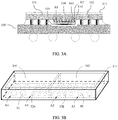
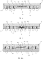
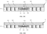
- FIG. 1 An existing fan-out package structure is shown in FIG. 1 .
- the fan-out package structure is a 2.5D FOP package structure combining a conventional fan-out wafer-level package and a flip chip (Flip Chip).
- a packaging process of the package structure is specifically as follows: First, a plurality of to-be-integrated dies 10 and 11 are placed in parallel on a carrier according to specific distances and locations, where a size of the carrier may be the same as an original size of a wafer. Then, the plurality of to-be-integrated dies 10 and 11 are molded by using a molding compound 12 to form a reconstructed wafer. Then, re-routing is performed on the reconstructed wafer, that is, a fan-out distribution layer 13 is manufactured on a front face of a die on the reconstructed wafer.
- the fan-out distribution layer 13 may electrically extend I/O pins on the dies 10 and 11 to an area outside the dies 10 and 11 through high-density interconnection structures 14 and 15. In this way, an electrical connection between the dies and a PCB board 16 is not limited to sizes and an arrangement of the dies 10 and 11.
- the package structure shown in FIG. 1 uses a wafer-level manufacturing process, so that both packaging and testing can be completed on a wafer. According to the package structure, a quantity of packaged pins can be effectively increased, and requirements of an advanced process node and a higher chip function for a larger quantity of pins can be met.
- the 2.5D FOP package can implement integration and packaging of a plurality of dies, and implement short-distance and high-density interconnection of dies through the fan-out distribution layer without through a substrate.
- the package structure has the following disadvantages:
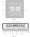
- the fan-out package structure is a 2.5D TSV package structure combining a flip chip and a silicon interposer (Si Interposer) having a through silicon via.
- the fan-out package structure is shown in FIG. 2 .
- a packaging process of the fan-out package structure is specifically as follows:
- a through silicon via 211 is manufactured on a silicon wafer, and a single layer of re-distribution layer 212 or a plurality of layers of re-distribution layers 212 are manufactured on a surface of the silicon wafer, to form a silicon interposer 21 used for signal connection.
- a plurality of to-be-integrated dies 22 and 23 are placed on a front face of the silicon interposer 21 according to pre-designed positions, and then the dies 22 and 23 are soldered to the front face of the silicon interposer 21 according to a soldering process.
- the 2.5D TSV package structure shown in FIG. 2 uses a silicon interposer and a TSV technology, and implements interconnection of different dies on a silicon wafer.
- An extremely minimum line width and an extremely minimum line distance are implemented by using a silicon material according to a mature semiconductor manufacturing process (currently, both a minimum line width and a minimum line distance of the silicon interposer are 0.4 ⁇ m), signal interconnection density of chips is greatly increased, and a signal routing distance is shortened.
- the package structure has the following advantages:
- a plurality of to-be-integrated dies need to be soldered on a silicon interposer.
- a size of the silicon interposer needs to be greater than a sum of sizes of all the dies, and more materials are consumed.
- an embodiment of this application provides a chip.
- a specific structure of the chip is a 2.5D substrate bridge across a fan-out package structure.
- the chip includes: a substrate 108, a fan-out unit 111, and a distribution layer 104, where the fan-out unit 111 includes a first chip 101 and a second chip 102.
- FIG. 3B schematically shows a structure of the fan-out unit 111, where hidden lines (invisible lines in a view direction) are represented by dashed lines.
- the first chip 101 includes a first pin array A1, and the first pin array A1 includes a plurality of first pins 32a.
- the second chip 102 includes a second pin array A2, and the second pin array A2 includes a plurality of second pins 32b.
- the fan-out unit 111 further includes a third pin array A3, and the third pin array A3 includes a plurality of third pins 41.
- the first pin array A1, the second pin array A2, and the third pin array A3 are all disposed facing the substrate 108. Surfaces that are of the first chip 101 and the second chip 102 and that face the substrate 108 are defined as front faces, and surfaces opposite to the front faces are defined as back faces.
- the first pin array A1, the second pin array A2, and the third pin array A3 are distributed on the front faces of the first chip 101 and the second chip 102.
- the first chip 101 and the second chip 102 are adjacently disposed
- the first pin array A1 and the second pin array A2 are adjacently disposed
- the third pin array A3 is distributed in an area, other than areas of the first pin array A1 and the second pin array A2, on the fan-out unit 111. That the first chip 101 and the second chip 102 are adjacently disposed indicates that the first chip 101 and the second chip 102 are not separated from each other by another chip.
- the distribution layer 104 is bridged between the first pin array A1 and the second pin array A2, and is used to connect the first pins 32a in the first pin array A1 to the corresponding second pins 32b in the second pin array A2.
- a manufacturing process of the distribution layer 104 is simple (which can be implemented according to a common build-up process), and costs are low.
- the third pin array A3 is directly connected to the substrate 108, so that a large-area intermediate board does not need to be disposed for a connection between the fan-out unit 111 and the substrate 108, and a process of manufacturing a through via on the intermediate board is omitted. Therefore, the chip shown in FIG. 3A has advantages of low process difficulties and low costs.
- the third pins in the third pin array A3 on the fan-out unit 111 can be connected to a periphery of the chip only through the substrate 108.
- components that affect an overall size of the chip include the fan-out unit 111 and the substrate 108. Consequently, the overall size of the chip is relatively large, and a requirement on chip miniaturization cannot be met.
- an embodiment of this application provides another structure of the chip.
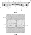
- FIG. 4 is a schematic sectional view of a chip structure according to an embodiment of this application.
- FIG. 4' is a top view of the chip structure according to this embodiment of this application.
- the chip provided in this embodiment of this application includes: a fan-out unit 31, a first substrate 32, and a molding body 33.
- the fan-out unit 31 includes a plurality of dies 341 and 342 that are integrated together and that are arranged according to preset positions.
- the plurality of dies integrated together may be two dies, or may be more than two dies.
- an example in which the plurality of to-be-integrated dies are two dies is used for description.
- the dies 341 and 342 may be integrated together by using a molding compound according to a molding process, to form the fan-out unit 31.
- a first pin array C1 and a second pin array C2 are disposed on the first surface of the die 341 or 342; the first pin array C1 includes a plurality of first pins 351, and the second pin array C2 includes a plurality of second pins 352; and second pin arrays C2 on adjacent dies are adjacent; and the first substrate 32 includes a first surface, a first re-distribution layer 321 and a first solder pad array electrically connected to the first re-distribution layer 321 are disposed on the first surface of the first substrate 32, and the first solder pad array includes a plurality of first solder pads 322.
- the first surfaces of the dies 341 and 342 are opposite to the first surface of the first substrate 32, the first substrate 32 is located below the fan-out unit 31, the first solder pad array is disposed opposite to the second pin array C2, and each second pin 352 in the second pin array C2 is attached to a corresponding first solder pad 322 in the first solder pad array, so that the different dies 341 and 342 are interconnected through the first re-distribution layer 321 on the first substrate 32.
- the molding body 33 is used to wrap the first pin 351, the second pin 352, the first solder pad 322, and the first substrate 32, so that the fan-out unit 31 and the first substrate 32 are molded into an integral structure.
- the molding body 33 is formed according to a molding process after the first solder pad array on the first substrate 32 and the second pin arrays C2 on the dies 341 and 342 are attached together.
- the molding process may be specifically a compression molding process (compression mold process). Therefore, the molding body 33 wraps at least a side face of the first pin 351, a side face of the second pin 352, a side face of the first solder pad 322, and a side face of the first substrate 32.
- the molding body 33 does not wrap bottoms of the first pins 351. In other words, the bottoms of the first pins 351 are exposed outside the molding body 33.
- the molding body 33 may further wrap a back face of the first substrate 32, so that an area in which the first pin array is molded and an area in which the first substrate 32 is located are of a flat-surface structure.
- a surface of the integral structure formed through molding is a flat surface.
- the structure has relatively low stability, and there is a relatively low possibility for the structure to work independently.
- the molding body 33 wraps the side face of the first pin 351, the side face of the second pin 352, and the side face of the first solder pad 322. In this way, a service life and reliability of the entire chip can be improved.
- the molding body 33 has a stable structure and high mechanical strength, the molding body 33 can effectively support independent use and work of the overall structure.
- the integral structure that is formed by molding the fan-out unit 31 and the first substrate 32 together according to the compression molding process can work stably and independently, or an RDL carrier board may be manufactured on the integral structure as required, or the integral structure may be bonded with a substrate as required, to form a larger package structure.
- a solder ball 36 may be disposed at the bottom of each first pin 351, and each solder ball 36 may be electrically connected to an external circuit such as a PCB board.
- a solder pad 37 may be further disposed between each first pin 351 and the solder ball 36.
- a molding material used to form the molding body 33 has different components from an underfill (under fill) in the prior art.
- the molding material and the underfill are obtained by adding different additives to an epoxy molding compound (Epoxy Molding Compound).
- the molding body 33 formed by using the molding material is generally implemented according to the compression molding process.
- the compression molding process is quite different from an underfill dispensing process.
- face-up type a to-be-molded structure is placed below a flowing molding material, the flowing molding material flows downward and is perfused on the to-be-molded structure, and then a mold is used to press-fit the perfused structure.
- a to-be-molded structure is placed above a container containing a flowing molding material, the to-be-molded structure is immersed into the container containing the flowing molding material, the to-be-molded structure is taken out from the container, and then a mold is used to press-fit the to-be-molded structure.
- the compression molding process can complete filling and curing of a large quantity of chips on an entire wafer at a time, and does not need to fill chips one by one, so that overall efficiency is relatively high.
- the curing in the compression molding process includes initial curing performed in a press-fitting state and final curing performed after the press-fitting is completed and the molded structure is placed in a heating furnace.
- a structure body with a stable structure can be formed by wrapping the die and the substrate by using the molding body 33, and the structure body can be directly mounted onto a terminal device.
- the underfill dispensing process is specifically as follows: When filling is performed by using an underfill, all chips on an entire wafer need to be dispensed one by one, and dispensing positions are on four edges of each chip, the underfill is attracted and filled into a gap between a chip and a substrate or another dielectric material through a capillary action, to complete a filling process. After the filling is completed, the filled structure is placed into the heating furnace to complete the final curing. Therefore, the filling process takes a relatively long time, and filling efficiency is relatively low.
- the underfill dispensing process needs to be performed after the structure formed by the fan-out unit 31 and the first substrate 32 is connected to another structure such as a substrate.
- filling, by using the molding material, the structure formed by the fan-out unit 31 and the first substrate 32 may be performed before the structure is connected to the another structure such as the substrate.
- the chip includes the fan-out unit 31, the first substrate 32, and the molding body 33.
- the first solder pads 351 in the first solder pad array C1 on the first substrate 32 are attached to the corresponding second pins 352 in the second pin arrays C2 on the different dies 341 and 342, to implement short-distance and high-density interconnection of the different dies.
- the molding body 33 is used to wrap the first pin 351, the second pin 352, and the first substrate 32, so that the fan-out unit 31 and the first substrate 32 are molded into an integral structure.
- the bottoms of the first pins that are in the first pin array C1 on the die and that are electrically connected to the periphery of the chip are not wrapped by the molding body 33. In this way, the first pins may be directly electrically connected to the periphery of the chip. Therefore, according to the chip provided in this embodiment of this application, a pin that is on the die and that is configured to electrically connect to the peripheral of the chip may be directly electrically connected to the peripheral of the chip, without using a substrate as an intermediary.
- An overall size of the chip provided in this embodiment of this application mainly depends on a size of the fan-out unit. The overall size of the chip provided in this embodiment of this application is smaller than that of a chip in the prior art, and a requirement on chip miniaturization can be met.
- a manner in which the dies 341 and 342 are interconnected through the first substrate 32 also facilitates the chip miniaturization.
- the first substrate 32 may be independently manufactured, and does not need to be directly manufactured on the fan-out unit 31. Therefore, if a defect occurs in a manufacturing process of the first substrate 32, a qualified die is not discarded, thereby reducing packaging costs.
- a size of the first substrate 32 is sufficient provided that the substrate 32 can be attached to the second pin 352 on the die, and the size does not need to be greater than or equal to a sum of sizes of all the dies integrated together. Therefore, in this embodiment of this application, materials consumed by the first substrate 32 can be reduced, and package costs can be greatly reduced. In addition, such a design is also conducive to the chip miniaturization.
- both a line width and a line distance of the first re-distribution layer on the first substrate 32 may reach 0.4 ⁇ m. Therefore, the line width and the line distance are relatively small, and a manufacturing process is relatively simple.
- the molding body 33 and the fan-out unit 31 may be of an integrally formed structure. In this case, the molding body 33 and the fan-out unit 31 may be obtained through compression molding in one time of molding process. In addition, in another specific embodiment of this application, the molding body 33 and the fan-out unit 31 may alternatively be of split structures. In this case, the molding body 33 and the fan-out unit 31 are obtained through compression molding in different times of molding processes.
- an embodiment of this application further provides an interconnection structure between the die 341 and the die 342. Details are shown in FIG. 6A and FIG. 6B .
- the first re-distribution layer 321 includes three layers of re-distribution sublayers, which may be respectively a first re-distribution sublayer, a second re-distribution sublayer, and a third re-distribution sublayer.
- the first re-distribution sublayer and the third re-distribution sublayer are used to implement interconnection of the dies 341 and 342, and a plane in which the second re-distribution sublayer is located is used as a reference plane of the re-distribution sublayers that are used to implement interconnection of the dies. In this way, signal quality can be improved and crosstalk between signals can be reduced.
- two interconnection structures are formed between the dies 341 and 342, and are respectively a first interconnection structure 51 and a second interconnection structure 52.
- the first interconnection structure 51 may be formed by the first re-distribution sublayer
- the second interconnection structure 52 may be formed by the third re-distribution sublayer.
- the second pin array on the die 341 includes a first pin group 511a configured to form the first interconnection structure 51 and a second pin group 512a configured to form the second interconnection structure.
- the second pin array on the die 342 includes a first pin group 511b configured to form the first interconnection structure 51 and a second pin group 512b configured to form the second interconnection structure.
- At least one interconnection structure may be formed between different dies, and each interconnection structure may include at least one interconnection line.
- each interconnection structure may include at least one interconnection line.
- the plurality of interconnection lines belonging to the same interconnection structure may have a same length or different lengths.
- all interconnection lines in a same interconnection structure have an equal length. Specifically, in FIG.
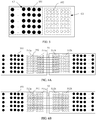
- connection structure columns in a same electrical connection structure group are sequentially named as a column 1, a column 2, and a column 3 in a sequence from left to right, and electrical connection structure rows are sequentially named as a row 1, a row 2, ..., until a row 7 in a sequence from up to down.
- first interconnection structure 51 a manner of connecting electrical connection structures in a row 1 in the first pin group 511a is shown in FIG. 6C .
- a solder joint in the row 1 and a column 1 in the first pin group 511a is connected to a solder joint in a row 1 and a column 1 in the first pin group 511b
- a solder joint in the row 1 and a column 2 in the first pin group 511a is connected to a solder joint in the row 1 and a column 2 in the first pin group 511b
- a solder joint in the row 1 and a column 3 in the first pin group 511a is connected to a solder joint in the row 1 and a column 3 in the first pin group 511b.
- Electrical connection structures in other rows are connected in a manner the same as a manner used for the electrical connection structures in the row 1. Details are not further described herein again.
- the first re-distribution layer 321 may be a single-layer distribution layer, or may be a multi-layer distribution layer.
- the first re-distribution layer includes a plurality of layers of first re-distribution sublayers, to improve signal quality and reduce crosstalk between signals, a plane in which any layer of first re-distribution sublayer is located is set as a reference plane of another first re-distribution sublayer, and the another first re-distribution sublayer is used to form an interconnection structure between different dies.
- the plurality of layers of distribution layers include a reference layer and a line layer, where a plane in which the reference layer is located is used as a reference plane of the line layer.
- the line layer is used to form an interconnection structure between different dies.
- an insulation dielectric layer may be disposed between different first re-distribution sublayers.
- the insulation dielectric layer may be an organic dielectric layer, for example, may be a dielectric layer made of a polymer material.
- the polymer material may be PI, PBO, or an epoxy resin-based polymer.
- a minimum size of a through via or a through via area on the insulation dielectric layer may reach 5 um/10 um or less.
- the first re-distribution layer 321 on the first substrate 32 and the first solder pad 322 in the first solder pad array each form an interconnection structure with the second pin 352 in the second pin array C2 on the dies 341 and 342.
- the die 341 and the die 342 are interconnected.
- the first re-distribution layer 321 on the first substrate 32 serves as a bridge connecting the die 341 and the die 342. Therefore, the first substrate 32 may be referred to as a bridge substrate.
- a cross-sectional size of the first substrate 32 is sufficient provided that the first substrate 32 can be attached to the second pin arrays on the dies 341 and 342, and the cross-sectional size does not need to be greater than a total size of a plurality of to-be-integrated dies. Therefore, the chip provided in this embodiment of this application consumes fewer materials.
- a distance between the dies needs to be as small as possible if a process condition allows.
- the distance between the dies may be 50 ⁇ m or even less.
- side faces of the dies 341 and 342 are wrapped by molding compound.
- an epitaxial width of the molding compound at outermost sides of the die 341 and the die 342 may be flexibly designed, and may be generally less than 5 mm.
- the molding compound at an outermost side of the fan-out unit 31 may extend epitaxially by a specific width in a thickness direction of the die as required, so that design of the substrate can be simplified and a quantity of layers of the substrate can be reduced.
- the dies 341 and 342 may be passive dies, or may be functional dies. More specifically, the dies 341 and 342 may be homogeneous or heterogeneous.
- the die may be integrated by an analog die and a digital die, integrated by dies of different process nodes, integrated by dies of different functions, or integrated by different quantities of dies after the dies are stacked.
- the dies 341 and 342 may be stacked dies.
- the first pin 351 is configured to lead out an I/O pin on a die to the periphery of the chip, and the second pin 352 is configured to implement interconnection of different dies. Therefore, to facilitate connection between a pin and a solder pad, in still another optional embodiment of this application, a size of the first pin 351 is greater than a size of the second pin 352. More specifically, a height of the first pin 351 is greater than a height of the second pin 352, and a cross-sectional size of the first pin 351 is also greater than a cross-sectional size of the second pin 352.
- a distance between two adjacent first pins 351 is a first distance d1
- a distance between two adjacent second pins 352 is a second distance d2.
- the first distance d1 may be greater than the second distance d2. This better facilitates connection between a pin and a corresponding solder pad.
- a cross-sectional size of a single first solder pad may be the same as a cross-sectional size of a single second pin.
- the first pin 351 may be a Cu pillar (Cu pillar), and the second pin 352 may be a solder bump (solder bump).
- Cu pillar Cu pillar
- solder bump solder bump
- the first solder pad 322 may be an electrical connection structure in various forms, and may be, for example, a solder bump, a protruding metal interface, or a flat metal plate.
- the solder bump may be a solder block.
- first pin 351 and the second pin 352 are not limited to specific pin structures in the foregoing examples.
- first pin 351 is not limited to the Cu pillar
- second pin 352 is not limited to the solder bump.
- the first pin 351 may be formed by at least one of the Cu pillar or the solder bump.
- the second pin 352 may be formed by at least one of the Cu pillar or the solder bump.
- each first pin 351 includes a Cu pillar part 3511 and a solder bump part 3512 that are connected to each other. It should be noted that, because the first pin 351 has a relatively large size, the first pin 351 uses a structure formed by the Cu pillar part 3511 and the solder bump part 3512 that are connected to each other, to facilitate manufacturing of the first pin 351.
- a gap between the first solder pads in the first solder pad array is relatively small, if a molding compound is used to fill the gap according to a molding process, a poor filling effect of the gap may be caused.
- an underfill 71 is filled in a gap between different first solder pads 322.
- a package structure shown in FIG. 8 is basically the same as the chip structure shown in FIG. 4 , and a difference only lies in that the chip structure shown in FIG. 8 includes the underfill 71 filled in the gap between the first solder pads 322 in the first solder pad array.
- a material for manufacturing the first substrate 32 may be any dielectric material such as a silicon-based material, a resin material, or a glass material. More specifically, the first substrate 32 may be a silicon substrate. In addition, the first substrate 32 may be a substrate processed by using a fan-out re-distribution layer technology. In this specific example, the first substrate 32 may be usually manufactured by using the resin material and an electrocoppering technology. In addition, the first substrate 32 may alternatively be a glass substrate on which an interconnection circuit is made on a surface. The interconnection circuit may be obtained by processing a glass material surface through etching and electroplating processes. It should be noted that, in this embodiment of this application, both the line width and the line distance of the first re-distribution layer on the first substrate 32 may reach 0.4 ⁇ m.
- the first substrate 32 is used to interconnect dies, and only a re-distribution layer and an electrical connection structure used for interconnection of dies are disposed on the first substrate 32.
- a through via 323 electrically connected to the first re-distribution layer 321 may be further disposed inside the first substrate 32.
- the through via 323 extends to a second surface of the first substrate 32.
- the second surface of the first substrate 32 is opposite to the first surface of the first substrate 32.
- the through via 323 may be electrically connected to a circuit on the periphery of the chip. In this way, electric energy on the periphery of the chip can be transmitted to the first re-distribution layer 321 through the first through via 323.
- a logical chip may be further disposed on the first substrate 32.
- a logical layer (not shown in FIG. 9 ) may be disposed inside the logical chip, and the logical layer is electrically connected to the through via 323. In this way, signal transmission between the logical layer and the outside can be implemented through the through via 323. In other words, the through via 323 can lead out a signal on the logical layer to the second surface of the first substrate 32, for signal transmission with the outside.
- the first pins 351 in the first pin array on the first surface of the die leads I/O pins on the die to a peripheral area of the chip. In this way, chip miniaturization can be implemented, and a requirement on miniaturization of a terminal consumer chip can be met.
- an electrical connection between the chip and the peripheral circuit of the chip is not limited to the sizes and the arrangement of the pins on the die.
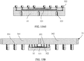
- a substrate that is used to directly electrically connect to the pins on the die may be further disposed below the molding body. For details, refer to FIG. 10A .
- a chip shown in FIG. 10A is obtained by improving the chip shown in FIG. 4 .
- another specific implementation of the chip provided in this embodiment of this application may further include: a second substrate 91, where the second substrate 91 is directly disposed below the molding body 33 according to a distribution layer build-up process.
- a second re-distribution layer (not shown in the figure) is disposed on the second substrate 91, and the second substrate 91 includes a first surface and a second surface that are opposite to each other.
- an embodiment of this application further provides a schematic diagram of the first surface structure of the second substrate 91.
- a second solder pad array electrically connected to the second re-distribution layer is disposed on the first surface of the second substrate 91, and the second solder pad array includes a plurality of second solder pads 911.
- the second solder pad 911 may be a metal bump or a metal solder pad, or may be a protruding metal interface.
- the metal bump may be a solder block.
- the second re-distribution layer may include a plurality of layers of re-distribution layers, and the plurality of layers of re-distribution layers may be evenly distributed in the entire thickness of the second substrate 91. In this way, the second re-distribution layer may be distributed not only on the first surface of the second substrate 91, but also inside the second substrate 91.
- a third solder pad array is disposed on the second surface of the second substrate 91, and the third solder pad array includes a plurality of third solder pads 912.
- the third solder pad 912 is used to implement an electrical connection between the chip and a peripheral circuit of the chip.
- the third solder pad 912 may be a metal solder ball.
- the second solder pad array is opposite to the first pin array, and each second solder pad 912 in the second solder pad array is electrically connected to a corresponding first pin 351 in the first pin array.
- the first pins 351 in the first pin arrays on the dies 341 and 342 are electrically connected to the corresponding second solder pads in the second solder pad array on the second substrate 91, and each third solder pad in the third solder pad array on the second substrate 91 is electrically connected to the peripheral circuit of the chip.
- the first pins 351 on the dies 341 and 342 are electrically connected to the peripheral circuit of the chip by using the second substrate 91. Because the second substrate 91 can provide larger line design space, density of the third solder pads 912 on the second substrate 91 may be less than density of the first pins 351 on the die.
- the third solder pads 912 on the second substrate 91 may be relatively easily electrically connected to the peripheral circuit of the chip through a soldering process. Therefore, even if the chip provided in this embodiment of this application includes a die with high pin density, the electrical connection between the die and the peripheral circuit of the chip can be easily implemented. Therefore, in the chip shown in FIG. 10A , the electrical connection between the chip and the peripheral circuit of the chip is no longer limited by sizes and an arrangement of pins on the die. Therefore, based on the chip structure, limitations caused by the arrangement of the pins on the die on the electrical connection between the chip and the peripheral circuit of the chip can be reduced.
- a first substrate 32 may be in contact with the second substrate 91.
- the first substrate 32 may not be in contact with the second substrate 91, and there is a gap between the first substrate 32 and the second substrate 91.
- the first substrate 32 is suspended above the second substrate 91. More specifically, in this embodiment of this application, provided that the first substrate 32 can be placed between a fan-out unit 31 and the second substrate 91, the thickness of the first substrate 32 is not specifically limited.
- a cross-sectional size of the second substrate 91 may be equivalent to a cross-sectional size of the fan-out unit 31. In this way, package structure miniaturization can be implemented, and a requirement on miniaturization of a terminal consumer chip can be met.
- the second substrate 91 may be directly manufactured on a surface that is of a molding body 33 and that is away from the fan-out unit 31.
- a dielectric layer for example, a PI/PBO material
- a copper conductive line is grown on a surface of the dielectric layer and stacked layer by layer until the second re-distribution layer is manufactured.
- the second solder pad array corresponding to the first pin array is manufactured at a position opposite to the first pin array.
- a dielectric layer is continued to be coated, and then the third solder pad array including the plurality of third solder pads 912 is manufactured on a surface of the dielectric layer.
- the second substrate 91 is used to lead out an I/O pin on a die to a peripheral area of the chip, to implement an electrical connection between the chip and a PCB board.
- the second substrate 91 can provide relatively large line design space, to facilitate the electrical connection between the chip and the peripheral circuit of the chip.
- an embodiment of this application further provides another specific implementation of the chip.
- FIG. 11 is a schematic sectional view of another chip according to this embodiment of this application.
- FIG. 11' is a top view of another chip structure according to this embodiment of this application.
- the chip structures shown in FIG. 11 and FIG. 11' are obtained by improving the chip structure shown in FIG. 10A .
- another specific implementation of the chip structure provided in this embodiment of this application may further include: a third substrate 101 disposed below the second substrate 91, where the third substrate 101 includes a first surface and a second surface that are opposite to each other, a fourth solder pad array is disposed on the first surface of the third substrate 101, and a fifth solder pad array is disposed on the second surface of the third substrate 101.
- the fourth solder pad array includes a plurality of fourth solder pads 1011
- the fifth solder pad array includes a plurality of fifth solder pads 1012.
- the fourth solder pad array is opposite to the third solder pad array, and each fourth solder pad 1011 in the fourth solder pad array is electrically connected to a corresponding third solder pad 912 in the third solder pad array.
- the fifth solder pad 1012 in the fifth solder pad array is used to implement signal transmission between the chip and a periphery of the chip.
- the fourth solder pad 1011 may be a metal bump
- the fifth solder pad 1012 may be a metal solder ball.
- the metal solder ball may be a solder ball, and is connected to a PCB board in a soldering manner.
- the fifth solder pad 1012 may be a metal solder plate, and is connected to a PCB board in a peripheral area in a socket (socket) manner.
- a cross-sectional size of the third substrate 101 may be greater than a cross-sectional size of the fan-out unit 31.
- the cross-sectional size of the third substrate 101 may be equal to the cross-sectional size of the fan-out unit 31.
- I/O pins on a die are led out to the peripheral area of the chip by using the second substrate 91 and the third substrate 101 through routing.
- the I/O pins on the die are led out by using the two substrates, so that routing resources of the chip structure and a quantity of packaged pins are increased, integrity of a packaged power supply is improved, and board-level reliability of the chip structure is improved.
- the chip structure shown in FIG. 11 may further include an underfill 102 filled between the second substrate 91 and the third substrate 101.
- this embodiment of this application further provides still another specific implementation of the chip structure.
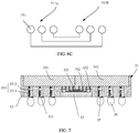
- a package structure shown in FIG. 12 is obtained by improving the chip structure shown in FIG. 11 . Therefore, in addition to the components of the package structure shown in FIG. 11 , a package structure shown in FIG. 12 may further include: heat sinks 111 disposed on the second surfaces of the dies 341 and 342, where the second surfaces of the dies 341 and 342 are opposite to the first surfaces of the dies 341 and 342.
- the heat sinks 111 may be bonded to the second surfaces of the dies 341 and 342 by using a thermal adhesive, so that a desirable heat dissipation approach can be provided for a chip with high power consumption.
- a second surface of each die is not wrapped by a molding compound, and if a heat dissipation requirement is met, the second surface of each die may be wrapped by the molding compound. It should be noted that if the die has relatively low power and generates less heat, the second surface of each die may be wrapped by the molding compound.
- the heat sink 111 may be connected to the third substrate 101. More specifically, the heat sink 111 may be bonded to a front face of the third substrate 101 by using an adhesive.
- the heat sink 111 may have an integral structure, or may have a split structure.
- the heat sink 111 may have a cap-shaped structure or a curved structure.
- the heat sink 111 masks the fan-out unit 31, and an edge of the heat sink 111 is fastened on the third substrate 101.
- FIG. 13 is a top view of a fan-out wafer-level package structure integrated by four dies. As shown in FIG. 13 , the integrated four dies 341 to 344 are interconnected through a first substrate 32.
- Apackaging method for a fan-out wafer-level package structure includes the following steps.
- S141 Separately manufacture a fan-out unit 31 and a first substrate 32.
- an implementation of manufacturing the fan-out unit 31 may specifically include the following steps: A1: Thin an original wafer of a die according to a design requirement, and then cut the thinned wafer into single dies.
- a first pin window array and a second pin window array are disposed on a first surface of each die.
- the first pin window array includes a plurality of first pin windows spaced by a first distance d1
- the second pin window array includes a plurality of second pin windows spaced by a second distance d2.
- a size of the first pin window is greater than a size of the second pin window, and the first distance d1 is greater than the second distance d2.
- A2 Arrange a plurality of to-be-integrated dies 341 and 342 according to preset positions and place the dies 341 and 342 on a temporary carrier 140.
- the plurality of to-be-integrated dies 341 and 342 are arranged according to the preset positions and placed on the temporary carrier 140.
- a size of the temporary carrier 140 may be the same as a size of the original wafer.
- the temporary carrier 140 may be a film material layer, and the film material layer may be a film made of a resin-type material.
- a distance between the dies needs to be as small as possible on a premise that a process condition allows.
- the distance between the dies may be 50 ⁇ m or even less.
- Side faces of the dies 341 and 342 are wrapped by a molding compound.
- an epitaxial width of the molding compound at outermost sides of the die 341 and the die 342 may be flexibly designed, and may be generally less than 5 mm.
- the molding compound at an outermost side of the fan-out unit 31 may extend epitaxially by a specific width in a thickness direction of the die, so that design of the substrate can be simplified and a quantity of layers of the substrate can be reduced.
- A3 Mold, by using a molding compound, the plurality of dies 341 and 342 placed on the temporary carrier 140, to form the fan-out unit 31.
- the plurality of dies molded together are taken out from the temporary carrier, and the plurality of dies molded together form the fan-out unit.
- the formed fan-out unit 31 is shown in FIG. 15A2 .
- a side face of each die is wrapped by the molding compound 141.
- a front face of each die is not wrapped by the molding compound, that is, the front face of each die is exposed to the outside. In this way, the first pin window array and the second pin window array of each die are exposed to the outside.
- A4 Form a first pin 351 in each first pin window in the first pin window array on each die, to form a first pin array C1, and form a second pin 352 in the second pin window on each die, to form a second pin array C2.
- the first pin 351 is formed in each first pin window in the first pin window array on each die, to form the first pin array C1
- the second pin 352 is formed in the second pin window on each die, to form the second pin array C2.
- the first pin 351 may be a Cu pillar
- the second pin 352 may be a solder bump.
- under bump metallization further needs to be formed on a surface of each first pin window and a surface of each second pin window.
- the first substrate 32 may be provided with a through via for signal transmission with the outside, or may not be provided with a through via for signal transmission with the outside.
- the specific implementation of the first substrate 32 not provided with a through via for signal transmission with the outside is described.
- the implementation of manufacturing the first substrate 32 may specifically include the following steps:
- B1 Divide a surface of an original wafer into a first area and a second area according to a design requirement of a package structure.
- B2 Manufacture a first re-distribution layer 321 in the first area of the original wafer, then manufacture each piece of under bump metallization in the second area of the original wafer, and manufacture a first solder pad 322 above each piece of under bump metallization, to form a first solder pad array.
- each piece of under bump metallization may be manufactured in the second area in a manner of electroplating or solder ball attachment.
- the first solder pad 322 may be a Cu pillar, or may be a metal bump.
- FIG. 15A4 a schematic sectional structural view of the formed single first substrate 32 is shown in FIG. 15A4 .
- the implementation of manufacturing the first substrate 32 may include the following steps:
- each piece of under bump metallization may be manufactured in the second area in a manner of electroplating or solder ball attachment.
- the first solder pad 322 may be a Cu pillar, or may be a solder bump.
- B'3 Provide a through via inside the original wafer, where the through via is electrically connected to the first re-distribution layer 321.
- the through via may be provided inside the original wafer through a TSV process.
- B'4 Manufacture a metal solder pad electrically connected to the through via on a back of the original wafer.
- FIG. 15A5 the schematic sectional structural view of the formed single first substrate 32 is shown in FIG. 15A5 .
- S142 Place the first substrate 32 below the fan-out unit 31, and attach each second pin 352 in the second pin array to a corresponding first solder pad 322 in the first solder pad array, so that different dies 341 and 342 are interconnected through the first substrate 32.
- the dies are interconnected through the first substrate 32. Therefore, as shown in FIG. 15B , the first solder pads in the first solder pad array disposed on the first surface of the first substrate 32 are attached to and connected to the corresponding second pins 352 in the second pin array on the dies 341 and 342. Therefore, the different dies are interconnected through the first re-distribution layer 321 disposed on the first substrate 32.
- the first substrate 32 and the fan-out unit 31 may be connected through mass reflow (Mass Reflow) or thermo compression bonding (Thermo Compression Bonding).
- S143 Mold, by using a molding compound, the fan-out unit 31 and the first substrate 32 that are attached together, to form a molding body 33 that wraps the first pins 351, the second pins 352, and the first substrate 32.
- FIG. 15C is a corresponding schematic sectional structural view after this step is performed.
- first pins 351 and the second pins 352 are wrapped by the molding compound, formation of the molding body 33 can improve reliability of the entire package structure.
- S144 Grind a surface that is of the molding body 33 and that is away from the fan-out unit 31, to expose bottoms of the first pins in the first pin array.
- This step may be specifically: grinding the surface that is of the molding body 33 and that is away from the fan-out unit 31 by using a mechanical grinding method, to expose the bottoms of the first pins 351 in the first pin array.
- FIG. 15D is a corresponding schematic sectional structural view after this step is performed.
- S145 Form, at the exposed bottoms of the first pins 351, solder balls 36 electrically connected to the outside.
- solder balls 36 are formed at the exposed bottoms of the first pins 351.
- a solder pad 37 may be further formed between each first pin 351 and the solder ball 36.
- the foregoing is the specific implementation of the chip packaging method provided in the embodiments of this application.
- short-distance and high-density interconnection of dies is implemented by using the first substrate 32.
- the molding body 33 is used to wrap the first pin 351, the second pin 352, and the first substrate 32, so that the fan-out unit 31 and the first substrate 32 are molded into an integral structure.
- bottoms of first pins that are in the first pin array on the die 341 and 342 and that are electrically connected to a periphery of the chip are not wrapped by the molding body 33. In this way, the first pins may be directly electrically connected to the periphery of the chip.
- an overall size of the chip provided in this embodiment of this application mainly depends on a size of a plurality of dies integrated together.
- the overall size of the chip provided in this embodiment of this application is relatively small compared with that of a chip in the prior art, and can meet a requirement on chip miniaturization.
- a manner in which the dies 341 and 342 are interconnected through the first substrate 32 also facilitates the chip miniaturization.
- the first substrate 32 may be independently manufactured, and does not need to be manufactured on dies integrated together. Therefore, if a defect occurs in a manufacturing process of the first substrate 32, a qualified die is not discarded, thereby reducing packaging costs.
- a size of the first substrate 32 is sufficient provided that the substrate 32 can be attached to the second pin 352 on the die, and the size does not need to be greater than or equal to a sum of sizes of all the dies integrated together. Therefore, in this embodiment of this application, materials consumed by the first substrate 32 can be reduced, and package costs can be greatly reduced. On the other hand, such a design is also conducive to the chip miniaturization.
- both a line width and a line distance of the first re-distribution layer on the first substrate 32 may reach 0.4 ⁇ m. Therefore, the line width and the line distance are relatively small, and a manufacturing process is relatively simple.
- the first pin 351 may be connected to an external circuit by using a substrate, so that the electrical connection between the chip and the peripheral circuit of the chip is not limited to sizes and an arrangement of the pins on the die. Based on this, an embodiment of this application further provides another implementation of the chip packaging method.
- the another chip packaging method provided in this embodiment of this application includes the following steps:
- This step may specifically include: A dielectric layer is coated on the ground surface that is of the molding body 33 and that is away from the fan-out unit 31, then a re-distribution layer is manufactured on a surface of the dielectric layer, and the re-distribution layer is stacked layer by layer until the second re-distribution layer is manufactured (where the second re-distribution layer is not shown in the figure).
- the second solder pad array corresponding to the first pin array is manufactured at a position opposite to the first pin array.
- the second solder pad array includes a plurality of second solder pads 911; and the second solder pads 911 are electrically connected to the second re-distribution layer.
- the third solder pad array includes a plurality of third solder pads 912.
- FIG. 10A is a corresponding schematic sectional structural view after S165 is performed.
- the second substrate 91 is directly manufactured on the surface that is of the molding body 33 and that is away from the fan-out unit 31. After the second substrate 91 is manufactured, the first pin on the die can be electrically connected to the second substrate 91.
- the second substrate 91 may also be referred to as an RDL carrier board.
- the second substrate 91 is directly manufactured on the ground surface that is of the molding body 33 and that is away from the fan-out unit 31. Therefore, a cross-sectional size of the first substrate 91 is the same as a cross-sectional size of the molding body 33.
- the cross-sectional size of the molding body 33 is the same as a cross-sectional size of the fan-out unit 31. Therefore, the cross-sectional size of the first substrate 91 is the same as the cross-sectional size of the fan-out unit 31.
- the first pins 351 in the first pin array on the dies 341 and 342 are electrically connected to the corresponding second solder pads in the second solder pad array on the second substrate 91, and each third solder pad in the third solder pad array on the second substrate 91 is electrically connected to the peripheral circuit of the chip.
- the first pins 351 on the dies 341 and 342 are electrically connected to the peripheral circuit of the chip by using the second substrate 91. Because the second substrate 91 can provide larger line design space, density of the third solder pads 912 on the second substrate 91 may be less than density of the first pins 351 on the die.
- the third solder pads 912 on the second substrate 91 may be relatively easily electrically connected to the peripheral circuit of the chip through a soldering process. Therefore, even if the chip formed according to this embodiment of this application includes a die with high pin density, the electrical connection between the die and the peripheral circuit of the chip can be easily implemented. Therefore, based on the chip structure formed according to this embodiment, the limitations caused by the arrangement of the pins on the die on the electrical connection between the chip and the peripheral circuit of the chip can be reduced.
- steps S1 and S2 may be further included.
- the third substrate 101 includes a first surface and a second surface that are opposite to each other, a fourth solder pad array is disposed on the first surface of the third substrate 101, a fifth solder pad array is disposed on the second surface of the third substrate 101, the fourth solder pad array includes a plurality of fourth solder pads 1011, and the fifth solder pad array includes a plurality of fifth solder pads 1012.
- the fourth solder pads in the fourth solder pad array on the third substrate 101 correspond to third solder pads in a third solder pad array on a second substrate 91.
- the fifth solder pads 1012 in the fifth solder pad array on the third substrate 101 are configured to electrically connect to a peripheral circuit of a chip. More specifically, the fifth solder pads 1012 in the fifth solder pad array on the third substrate 101 are configured to electrically connect to a PCB board in a peripheral area of the chip.
- the third solder pads 912 in the third solder pad array on the second substrate 91 are no longer configured to connect to an external circuit, but are configured to connect to the fourth solder pads 1011 in the fourth solder pad array on the first surface of the third substrate 101.
- the fifth solder pads 1012 in the fifth solder pad array on the second surface of the third substrate 101 are electrically connected to the PCB board in the peripheral area of the chip.
- the chip packaging method provided in this embodiment of this application may further include: S2: Place the third substrate 101 below the second substrate 91, and attach each fourth solder pad 1011 in the fourth solder pad array to the corresponding third solder pad 912 in the third solder pad array, so that each fourth solder pad 1011 in the fourth solder pad array is electrically connected to the corresponding third solder pad 912 in the third solder pad array.
- the packaging method in the foregoing optional embodiment may further include the following step after S2: S3: Fill an underfill 102 between the second substrate 91 and the third substrate 101.
- FIG. 11 is a corresponding schematic sectional structural view after this step is performed.
- the molding compound may not completely wrap the first solder pads 322, causing a decrease in the reliability of the entire chip structure.
- the following step may be further included: S4: Fill the underfill 71 in a gap between the first solder pads 322 in the first solder pad array.
- FIG. 8 is a corresponding schematic sectional structural view after this step is performed.
- the following step may be further included: S5: Dispose a heat sink 111 on the second surface of the die.
- FIG. 12 is a corresponding schematic sectional structural view after this step is performed.
- the heat sinks 111 may be bonded to the second surfaces of the die by using a thermal adhesive, so that a desirable heat dissipation approach can be provided for a chip with high power consumption.
- S6 Grind a surface that is of the fan-out unit 31 and that is away from the second substrate 91, to expose the second surfaces of the dies 341 and 342.
- the heat sink 111 may be further connected to the third substrate 101. Therefore, in still another optional embodiment of this application, based on the foregoing optional embodiment, the following step may be further included: S7: Mask the fan-out unit 31 in the heat sink 111, and fasten an edge of the heat sink 111 to the third substrate 101.
- the heat sink 111 may be bonded to the first surface of the third substrate 101 by using an adhesive.
Landscapes
- Encapsulation Of And Coatings For Semiconductor Or Solid State Devices (AREA)
- Structures Or Materials For Encapsulating Or Coating Semiconductor Devices Or Solid State Devices (AREA)
- Production Of Multi-Layered Print Wiring Board (AREA)
- Cooling Or The Like Of Semiconductors Or Solid State Devices (AREA)
- Physics & Mathematics (AREA)
- Geometry (AREA)
- Engineering & Computer Science (AREA)
- Manufacturing & Machinery (AREA)
Applications Claiming Priority (2)
| Application Number | Priority Date | Filing Date | Title |
|---|---|---|---|
| CN201810157259.5A CN110197793A (zh) | 2018-02-24 | 2018-02-24 | 一种芯片及封装方法 |
| PCT/CN2018/099006 WO2019161641A1 (zh) | 2018-02-24 | 2018-08-06 | 一种芯片及封装方法 |
Publications (2)
| Publication Number | Publication Date |
|---|---|
| EP3748672A1 true EP3748672A1 (de) | 2020-12-09 |
| EP3748672A4 EP3748672A4 (de) | 2021-04-21 |
Family
ID=67687975
Family Applications (1)
| Application Number | Title | Priority Date | Filing Date |
|---|---|---|---|
| EP18906810.9A Pending EP3748672A4 (de) | 2018-02-24 | 2018-08-06 | Chip und verpackungsverfahren |
Country Status (4)
| Country | Link |
|---|---|
| US (1) | US11276645B2 (de) |
| EP (1) | EP3748672A4 (de) |
| CN (2) | CN110197793A (de) |
| WO (1) | WO2019161641A1 (de) |
Cited By (3)
| Publication number | Priority date | Publication date | Assignee | Title |
|---|---|---|---|---|
| EP3828925A1 (de) * | 2019-11-27 | 2021-06-02 | INTEL Corporation | Zusammengesetzte interposerstruktur und verfahren zu deren herstellung |
| EP3826051A3 (de) * | 2020-06-19 | 2021-10-20 | Beijing Baidu Netcom Science And Technology Co. Ltd. | Chip-gehäuse und elektronische vorrichtung |
| CN115172178A (zh) * | 2022-08-04 | 2022-10-11 | 江苏中科智芯集成科技有限公司 | 一种利用载板的芯片垂直集成封装结构及其制备方法 |
Families Citing this family (43)
| Publication number | Priority date | Publication date | Assignee | Title |
|---|---|---|---|---|
| US11756889B2 (en) * | 2019-08-07 | 2023-09-12 | Intel Corporation | Ultrathin bridge and multi-die ultrafine pitch patch architecture and method of making |
| US11569172B2 (en) * | 2019-08-08 | 2023-01-31 | Taiwan Semiconductor Manufacturing Co., Ltd. | Semiconductor devices and methods of manufacture |
| DE102020115288A1 (de) * | 2019-08-08 | 2021-02-11 | Taiwan Semiconductor Manufacturing Co., Ltd. | Halbleitervorrichtungen und herstellungsverfahren |
| JP7652360B2 (ja) | 2019-12-11 | 2025-03-27 | インテル・コーポレーション | 集積回路パッケージのためのコンポジットブリッジダイツーダイ相互接続 |
| US11616026B2 (en) | 2020-01-17 | 2023-03-28 | Taiwan Semiconductor Manufacturing Company, Ltd. | Semiconductor device and method of manufacture |
| CN112309993A (zh) * | 2020-02-17 | 2021-02-02 | 成都华微电子科技有限公司 | 基于硅基封装基板的封装结构 |
| CN111354718B (zh) * | 2020-03-23 | 2022-02-25 | 江苏中科智芯集成科技有限公司 | 含多芯片封装结构的芯片排列布线方法、装置及电子设备 |
| US12027448B2 (en) * | 2020-03-24 | 2024-07-02 | Intel Corporation | Open cavity bridge power delivery architectures and processes |
| CN111554628B (zh) * | 2020-04-30 | 2023-05-16 | 通富微电子股份有限公司 | 一种芯片封装方法 |
| CN111554613A (zh) * | 2020-04-30 | 2020-08-18 | 通富微电子股份有限公司 | 一种芯片封装方法 |
| CN111554625A (zh) * | 2020-04-30 | 2020-08-18 | 通富微电子股份有限公司 | 一种芯片封装方法 |
| CN111554622B (zh) * | 2020-04-30 | 2023-07-14 | 通富微电子股份有限公司 | 一种芯片封装方法 |
| CN111554655A (zh) * | 2020-04-30 | 2020-08-18 | 通富微电子股份有限公司 | 一种半导体封装器件 |
| CN111554656A (zh) * | 2020-04-30 | 2020-08-18 | 通富微电子股份有限公司 | 一种半导体封装器件 |
| CN111554657B (zh) * | 2020-04-30 | 2023-07-14 | 通富微电子股份有限公司 | 一种半导体封装器件 |
| CN111554626A (zh) * | 2020-04-30 | 2020-08-18 | 通富微电子股份有限公司 | 一种芯片封装方法 |
| CN111554658A (zh) * | 2020-04-30 | 2020-08-18 | 通富微电子股份有限公司 | 一种半导体封装器件 |
| CN111769099B (zh) * | 2020-07-09 | 2022-03-04 | 中国科学院微电子研究所 | 一种基于多转接板实现多芯片集成的封装结构及封装方法 |
| CN113937018A (zh) * | 2020-07-14 | 2022-01-14 | 中芯集成电路(宁波)有限公司上海分公司 | 晶圆级封装方法以及封装结构 |
| US12575432B2 (en) | 2020-07-27 | 2026-03-10 | Shenzhen Xiuyuan Electronic Technology Co., Ltd. | Chip fine line fan-out package structure and manufacturing method therefor |
| US11658123B2 (en) * | 2020-09-25 | 2023-05-23 | Advanced Micro Devices, Inc. | Hybrid bridged fanout chiplet connectivity |
| CN112243312A (zh) * | 2020-10-16 | 2021-01-19 | 恒为科技(上海)股份有限公司 | 一种pcb板及其制备方法 |
| TWI767365B (zh) * | 2020-10-16 | 2022-06-11 | 大陸商青島新核芯科技有限公司 | 封裝結構及其製備方法 |
| CN114388488A (zh) | 2020-10-16 | 2022-04-22 | 虹晶科技股份有限公司 | 封装结构及其制备方法 |
| US12355000B2 (en) | 2020-11-10 | 2025-07-08 | Qualcomm Incorporated | Package comprising a substrate and a high-density interconnect integrated device |
| CN112542392B (zh) * | 2020-12-04 | 2021-10-22 | 上海易卜半导体有限公司 | 一种形成封装件的方法及封装件 |
| CN112542391B (zh) * | 2020-12-04 | 2022-11-11 | 上海易卜半导体有限公司 | 芯片互联方法、互联器件以及形成封装件的方法 |
| CN112599427B (zh) * | 2020-12-04 | 2022-10-28 | 上海易卜半导体有限公司 | 一种形成封装件的方法及封装件 |
| US12224267B2 (en) | 2020-12-04 | 2025-02-11 | Yibu Semiconductor Co., Ltd. | Chip interconnecting method, interconnect device and method for forming chip packages |
| US12119326B2 (en) * | 2020-12-18 | 2024-10-15 | Intel Corporation | Microelectronic structures including bridges |
| US12469811B2 (en) | 2021-03-26 | 2025-11-11 | Qualcomm Incorporated | Package comprising wire bonds coupled to integrated devices |
| EP4340010B1 (de) * | 2021-07-14 | 2025-06-25 | Huawei Technologies Co., Ltd. | Chipgehäusestruktur und verpackungsverfahren und elektronische vorrichtung |
| CN114937609B (zh) * | 2022-04-15 | 2023-09-22 | 盛合晶微半导体(江阴)有限公司 | 一种2.5d/3d电子封装结构及其制备方法 |
| CN114937608B (zh) * | 2022-04-15 | 2023-08-08 | 盛合晶微半导体(江阴)有限公司 | 一种高密度互连的封装结构及其制备方法 |
| US12388047B2 (en) * | 2022-08-23 | 2025-08-12 | Taiwan Semiconductor Manufacturing Company, Ltd. | Integrated fan-out platform and manufacturing method for semiconductor devices |
| CN116998008A (zh) * | 2022-10-18 | 2023-11-03 | 广东省科学院半导体研究所 | 具备芯片间精细内互连线路的扇出封装结构及其制造方法 |
| CN115714121B (zh) * | 2022-11-10 | 2025-10-31 | 上海遇贤微电子有限公司 | 芯片互连结构及其制备方法和芯片封装结构 |
| CN116092956B (zh) * | 2023-04-10 | 2023-11-03 | 北京华封集芯电子有限公司 | 芯片封装方法及芯片封装结构 |
| CN119208290B (zh) * | 2023-06-16 | 2025-10-03 | 长鑫存储技术有限公司 | 信息处理装置 |
| TWI893456B (zh) * | 2023-09-21 | 2025-08-11 | 南韓商哈納米克羅恩公司 | 半導體封裝及其製造方法 |
| CN117056279B (zh) * | 2023-10-12 | 2024-01-26 | 之江实验室 | 可重构电路、可重构芯粒间互联的装置及其方法 |
| CN119890170A (zh) * | 2023-10-24 | 2025-04-25 | 华为技术有限公司 | 一种芯片封装系统及电子设备 |
| CN120413564A (zh) * | 2024-01-29 | 2025-08-01 | 华为技术有限公司 | 一种芯片封装结构、其制作方法及电子设备 |
Family Cites Families (17)
| Publication number | Priority date | Publication date | Assignee | Title |
|---|---|---|---|---|
| US6100196A (en) | 1996-04-08 | 2000-08-08 | Chartered Semiconductor Manufacturing Ltd. | Method of making a copper interconnect with top barrier layer |
| US8367475B2 (en) * | 2011-03-25 | 2013-02-05 | Broadcom Corporation | Chip scale package assembly in reconstitution panel process format |
| US8872349B2 (en) | 2012-09-11 | 2014-10-28 | Intel Corporation | Bridge interconnect with air gap in package assembly |
| US8946900B2 (en) | 2012-10-31 | 2015-02-03 | Intel Corporation | X-line routing for dense multi-chip-package interconnects |
| CN203573966U (zh) * | 2013-10-24 | 2014-04-30 | 天水华天科技股份有限公司 | 一种带焊球面阵列四面扁平无引脚封装件 |
| US9735043B2 (en) * | 2013-12-20 | 2017-08-15 | Taiwan Semiconductor Manufacturing Company, Ltd. | Semiconductor packaging structure and process |
| CN203774286U (zh) * | 2014-01-26 | 2014-08-13 | 深圳市兴森快捷电路科技股份有限公司 | 一种带散热装置的pop封装 |
| US9355997B2 (en) * | 2014-03-12 | 2016-05-31 | Invensas Corporation | Integrated circuit assemblies with reinforcement frames, and methods of manufacture |
| US9653428B1 (en) * | 2015-04-14 | 2017-05-16 | Amkor Technology, Inc. | Semiconductor package and fabricating method thereof |
| US9761533B2 (en) * | 2015-10-16 | 2017-09-12 | Xilinx, Inc. | Interposer-less stack die interconnect |
| US10163856B2 (en) * | 2015-10-30 | 2018-12-25 | Taiwan Semiconductor Manufacturing Company, Ltd. | Stacked integrated circuit structure and method of forming |
| CN109087908B (zh) * | 2015-12-31 | 2020-10-27 | 华为技术有限公司 | 封装结构、电子设备及封装方法 |
| US10833052B2 (en) * | 2016-10-06 | 2020-11-10 | Micron Technology, Inc. | Microelectronic package utilizing embedded bridge through-silicon-via interconnect component and related methods |
| US10510667B2 (en) * | 2016-12-21 | 2019-12-17 | Intel Corporation | Conductive coating for a microelectronics package |
| CN107104096A (zh) * | 2017-05-19 | 2017-08-29 | 华为技术有限公司 | 芯片封装结构及电路结构 |
| CN107479283B (zh) * | 2017-08-30 | 2020-07-07 | 厦门天马微电子有限公司 | 一种阵列基板、显示面板及显示装置 |
| CN111133575A (zh) * | 2017-12-29 | 2020-05-08 | 英特尔公司 | 具有通信网络的微电子组件 |
-
2018
- 2018-02-24 CN CN201810157259.5A patent/CN110197793A/zh active Pending
- 2018-02-24 CN CN202211696179.XA patent/CN116169110A/zh active Pending
- 2018-08-06 EP EP18906810.9A patent/EP3748672A4/de active Pending
- 2018-08-06 WO PCT/CN2018/099006 patent/WO2019161641A1/zh not_active Ceased
-
2020
- 2020-08-19 US US16/997,003 patent/US11276645B2/en active Active
Cited By (8)
| Publication number | Priority date | Publication date | Assignee | Title |
|---|---|---|---|---|
| EP3828925A1 (de) * | 2019-11-27 | 2021-06-02 | INTEL Corporation | Zusammengesetzte interposerstruktur und verfahren zu deren herstellung |
| US11270947B2 (en) | 2019-11-27 | 2022-03-08 | Intel Corporation | Composite interposer structure and method of providing same |
| US11652059B2 (en) | 2019-11-27 | 2023-05-16 | Intel Corporation | Composite interposer structure and method of providing same |
| US12014990B2 (en) | 2019-11-27 | 2024-06-18 | Intel Corporation | Composite interposer structure and method of providing same |
| US12362284B2 (en) | 2019-11-27 | 2025-07-15 | Intel Corporation | Composite interposer structure and method of providing same |
| EP3826051A3 (de) * | 2020-06-19 | 2021-10-20 | Beijing Baidu Netcom Science And Technology Co. Ltd. | Chip-gehäuse und elektronische vorrichtung |
| US11594465B2 (en) | 2020-06-19 | 2023-02-28 | Beijing Baidu Netcom Science And Technology Co., Ltd. | Chip package and electronic device |
| CN115172178A (zh) * | 2022-08-04 | 2022-10-11 | 江苏中科智芯集成科技有限公司 | 一种利用载板的芯片垂直集成封装结构及其制备方法 |
Also Published As
| Publication number | Publication date |
|---|---|
| CN110197793A (zh) | 2019-09-03 |
| WO2019161641A1 (zh) | 2019-08-29 |
| US11276645B2 (en) | 2022-03-15 |
| EP3748672A4 (de) | 2021-04-21 |
| CN116169110A (zh) | 2023-05-26 |
| US20200381361A1 (en) | 2020-12-03 |
Similar Documents
| Publication | Publication Date | Title |
|---|---|---|
| US11276645B2 (en) | Encapsulation of a substrate electrically connected to a plurality of pin arrays | |
| US10559525B2 (en) | Embedded silicon substrate fan-out type 3D packaging structure | |
| CN109087908B (zh) | 封装结构、电子设备及封装方法 | |
| US9806061B2 (en) | Bumpless wafer level fan-out package | |
| US6844619B2 (en) | Compact semiconductor device capable of mounting a plurality of semiconductor chips with high density and method of manufacturing the same | |
| US9117826B2 (en) | Method of manufacturing semiconductor device, and semiconductor device | |
| US20020074637A1 (en) | Stacked flip chip assemblies | |
| CN113257778A (zh) | 一种3d堆叠且背部导出的扇出型封装结构及其制造方法 | |
| TWI826339B (zh) | 2.5d封裝結構及製備方法 | |
| US20250372578A1 (en) | Semiconductor package having passive support wafer | |
| CN112038329A (zh) | 一种圆片级芯片扇出三维堆叠封装结构及其制作方法 | |
| US8354298B2 (en) | Semiconductor device and manufacturing method of a semiconductor device | |
| US20260114289A1 (en) | Fan-out chip packaging structure based on shielded metal carrier plate and method for manufacturing same | |
| US20240304556A1 (en) | Chiplet-fine-interconnection-package structure and method of manufacturing the same | |
| CN101179066B (zh) | 芯片嵌埋式封装结构 | |
| US20070020812A1 (en) | Circuit board structure integrated with semiconductor chip and method of fabricating the same | |
| CN1316611C (zh) | 具有增层结构的晶圆级半导体封装件及其制法 | |
| JP2021119630A (ja) | チップパッケージ構造及び電子機器 | |
| CN220233193U (zh) | 改善电源信号传输的2.5d封装结构 | |
| CN219832635U (zh) | 半导体封装结构 | |
| CN120727585A (zh) | 一种集成多种封装技术的超薄系统级芯片封装结构及方法 | |
| CN115472602A (zh) | 封装结构及其制作方法 | |
| TW202612108A (zh) | 半導體封裝組件 | |
| WO2026061105A9 (zh) | 封装基板及其制备方法、半导体堆叠结构、电子设备 | |
| CN119361559A (zh) | 一种多芯片3d堆叠的封装结构 |
Legal Events
| Date | Code | Title | Description |
|---|---|---|---|
| STAA | Information on the status of an ep patent application or granted ep patent |
Free format text: STATUS: THE INTERNATIONAL PUBLICATION HAS BEEN MADE |
|
| PUAI | Public reference made under article 153(3) epc to a published international application that has entered the european phase |
Free format text: ORIGINAL CODE: 0009012 |
|
| STAA | Information on the status of an ep patent application or granted ep patent |
Free format text: STATUS: REQUEST FOR EXAMINATION WAS MADE |
|
| 17P | Request for examination filed |
Effective date: 20200902 |
|
| AK | Designated contracting states |
Kind code of ref document: A1 Designated state(s): AL AT BE BG CH CY CZ DE DK EE ES FI FR GB GR HR HU IE IS IT LI LT LU LV MC MK MT NL NO PL PT RO RS SE SI SK SM TR |
|
| AX | Request for extension of the european patent |
Extension state: BA ME |
|
| RIC1 | Information provided on ipc code assigned before grant |
Ipc: H01L 21/60 20060101AFI20210201BHEP Ipc: H01L 23/498 20060101ALI20210201BHEP Ipc: H01L 25/065 20060101ALI20210201BHEP Ipc: H01L 21/56 20060101ALI20210201BHEP Ipc: H01L 23/31 20060101ALI20210201BHEP Ipc: H01L 23/538 20060101ALI20210201BHEP |
|
| REG | Reference to a national code |
Ref country code: DE Ref legal event code: R079 Free format text: PREVIOUS MAIN CLASS: H01L0023485000 Ipc: H01L0021600000 |
|
| A4 | Supplementary search report drawn up and despatched |
Effective date: 20210319 |
|
| RIC1 | Information provided on ipc code assigned before grant |
Ipc: H01L 21/60 20060101AFI20210315BHEP Ipc: H01L 25/065 20060101ALI20210315BHEP Ipc: H01L 21/56 20060101ALI20210315BHEP Ipc: H01L 23/538 20060101ALI20210315BHEP Ipc: H01L 23/31 20060101ALI20210315BHEP Ipc: H01L 23/498 20060101ALI20210315BHEP |
|
| DAV | Request for validation of the european patent (deleted) | ||
| DAX | Request for extension of the european patent (deleted) | ||
| STAA | Information on the status of an ep patent application or granted ep patent |
Free format text: STATUS: EXAMINATION IS IN PROGRESS |
|
| 17Q | First examination report despatched |
Effective date: 20240430 |