EP3748687A1 - Transistor à couches minces et son procédé de fabrication, substrat d'affichage et dispositif d'affichage - Google Patents
Transistor à couches minces et son procédé de fabrication, substrat d'affichage et dispositif d'affichage Download PDFInfo
- Publication number
- EP3748687A1 EP3748687A1 EP18903206.3A EP18903206A EP3748687A1 EP 3748687 A1 EP3748687 A1 EP 3748687A1 EP 18903206 A EP18903206 A EP 18903206A EP 3748687 A1 EP3748687 A1 EP 3748687A1
- Authority
- EP
- European Patent Office
- Prior art keywords
- layer
- gate electrode
- metal oxide
- forming
- thin film
- Prior art date
- Legal status (The legal status is an assumption and is not a legal conclusion. Google has not performed a legal analysis and makes no representation as to the accuracy of the status listed.)
- Withdrawn
Links
Images

Classifications
-
- H—ELECTRICITY
- H10—SEMICONDUCTOR DEVICES; ELECTRIC SOLID-STATE DEVICES NOT OTHERWISE PROVIDED FOR
- H10D—INORGANIC ELECTRIC SEMICONDUCTOR DEVICES
- H10D30/00—Field-effect transistors [FET]
- H10D30/01—Manufacture or treatment
- H10D30/021—Manufacture or treatment of FETs having insulated gates [IGFET]
- H10D30/031—Manufacture or treatment of FETs having insulated gates [IGFET] of thin-film transistors [TFT]
- H10D30/0312—Manufacture or treatment of FETs having insulated gates [IGFET] of thin-film transistors [TFT] characterised by the gate electrodes
- H10D30/0316—Manufacture or treatment of FETs having insulated gates [IGFET] of thin-film transistors [TFT] characterised by the gate electrodes of lateral bottom-gate TFTs comprising only a single gate
-
- H—ELECTRICITY
- H10—SEMICONDUCTOR DEVICES; ELECTRIC SOLID-STATE DEVICES NOT OTHERWISE PROVIDED FOR
- H10D—INORGANIC ELECTRIC SEMICONDUCTOR DEVICES
- H10D30/00—Field-effect transistors [FET]
- H10D30/01—Manufacture or treatment
- H10D30/021—Manufacture or treatment of FETs having insulated gates [IGFET]
- H10D30/031—Manufacture or treatment of FETs having insulated gates [IGFET] of thin-film transistors [TFT]
- H10D30/0321—Manufacture or treatment of FETs having insulated gates [IGFET] of thin-film transistors [TFT] comprising silicon, e.g. amorphous silicon or polysilicon
-
- H—ELECTRICITY
- H10—SEMICONDUCTOR DEVICES; ELECTRIC SOLID-STATE DEVICES NOT OTHERWISE PROVIDED FOR
- H10D—INORGANIC ELECTRIC SEMICONDUCTOR DEVICES
- H10D30/00—Field-effect transistors [FET]
- H10D30/60—Insulated-gate field-effect transistors [IGFET]
- H10D30/67—Thin-film transistors [TFT]
-
- H—ELECTRICITY
- H10—SEMICONDUCTOR DEVICES; ELECTRIC SOLID-STATE DEVICES NOT OTHERWISE PROVIDED FOR
- H10D—INORGANIC ELECTRIC SEMICONDUCTOR DEVICES
- H10D30/00—Field-effect transistors [FET]
- H10D30/60—Insulated-gate field-effect transistors [IGFET]
- H10D30/67—Thin-film transistors [TFT]
- H10D30/6729—Thin-film transistors [TFT] characterised by the electrodes
- H10D30/6737—Thin-film transistors [TFT] characterised by the electrodes characterised by the electrode materials
- H10D30/6739—Conductor-insulator-semiconductor electrodes
-
- H—ELECTRICITY
- H10—SEMICONDUCTOR DEVICES; ELECTRIC SOLID-STATE DEVICES NOT OTHERWISE PROVIDED FOR
- H10D—INORGANIC ELECTRIC SEMICONDUCTOR DEVICES
- H10D64/00—Electrodes of devices having potential barriers
- H10D64/60—Electrodes characterised by their materials
- H10D64/66—Electrodes having a conductor capacitively coupled to a semiconductor by an insulator, e.g. MIS electrodes
- H10D64/68—Electrodes having a conductor capacitively coupled to a semiconductor by an insulator, e.g. MIS electrodes characterised by the insulator, e.g. by the gate insulator
- H10D64/681—Electrodes having a conductor capacitively coupled to a semiconductor by an insulator, e.g. MIS electrodes characterised by the insulator, e.g. by the gate insulator having a compositional variation, e.g. multilayered
- H10D64/685—Electrodes having a conductor capacitively coupled to a semiconductor by an insulator, e.g. MIS electrodes characterised by the insulator, e.g. by the gate insulator having a compositional variation, e.g. multilayered being perpendicular to the channel plane
-
- H—ELECTRICITY
- H10—SEMICONDUCTOR DEVICES; ELECTRIC SOLID-STATE DEVICES NOT OTHERWISE PROVIDED FOR
- H10D—INORGANIC ELECTRIC SEMICONDUCTOR DEVICES
- H10D64/00—Electrodes of devices having potential barriers
- H10D64/60—Electrodes characterised by their materials
- H10D64/66—Electrodes having a conductor capacitively coupled to a semiconductor by an insulator, e.g. MIS electrodes
- H10D64/68—Electrodes having a conductor capacitively coupled to a semiconductor by an insulator, e.g. MIS electrodes characterised by the insulator, e.g. by the gate insulator
- H10D64/691—Electrodes having a conductor capacitively coupled to a semiconductor by an insulator, e.g. MIS electrodes characterised by the insulator, e.g. by the gate insulator comprising metallic compounds, e.g. metal oxides or metal silicates
-
- H—ELECTRICITY
- H10—SEMICONDUCTOR DEVICES; ELECTRIC SOLID-STATE DEVICES NOT OTHERWISE PROVIDED FOR
- H10D—INORGANIC ELECTRIC SEMICONDUCTOR DEVICES
- H10D64/00—Electrodes of devices having potential barriers
- H10D64/60—Electrodes characterised by their materials
- H10D64/66—Electrodes having a conductor capacitively coupled to a semiconductor by an insulator, e.g. MIS electrodes
- H10D64/68—Electrodes having a conductor capacitively coupled to a semiconductor by an insulator, e.g. MIS electrodes characterised by the insulator, e.g. by the gate insulator
- H10D64/693—Electrodes having a conductor capacitively coupled to a semiconductor by an insulator, e.g. MIS electrodes characterised by the insulator, e.g. by the gate insulator the insulator comprising nitrogen, e.g. nitrides, oxynitrides or nitrogen-doped materials
-
- H—ELECTRICITY
- H10—SEMICONDUCTOR DEVICES; ELECTRIC SOLID-STATE DEVICES NOT OTHERWISE PROVIDED FOR
- H10D—INORGANIC ELECTRIC SEMICONDUCTOR DEVICES
- H10D86/00—Integrated devices formed in or on insulating or conducting substrates, e.g. formed in silicon-on-insulator [SOI] substrates or on stainless steel or glass substrates
- H10D86/40—Integrated devices formed in or on insulating or conducting substrates, e.g. formed in silicon-on-insulator [SOI] substrates or on stainless steel or glass substrates characterised by multiple TFTs
- H10D86/60—Integrated devices formed in or on insulating or conducting substrates, e.g. formed in silicon-on-insulator [SOI] substrates or on stainless steel or glass substrates characterised by multiple TFTs wherein the TFTs are in active matrices
-
- H—ELECTRICITY
- H10—SEMICONDUCTOR DEVICES; ELECTRIC SOLID-STATE DEVICES NOT OTHERWISE PROVIDED FOR
- H10P—GENERIC PROCESSES OR APPARATUS FOR THE MANUFACTURE OR TREATMENT OF DEVICES COVERED BY CLASS H10
- H10P14/00—Formation of materials, e.g. in the shape of layers or pillars
- H10P14/60—Formation of materials, e.g. in the shape of layers or pillars of insulating materials
- H10P14/65—Formation of materials, e.g. in the shape of layers or pillars of insulating materials characterised by treatments performed before or after the formation of the materials
- H10P14/6516—Formation of materials, e.g. in the shape of layers or pillars of insulating materials characterised by treatments performed before or after the formation of the materials of treatments performed after formation of the materials
- H10P14/6529—Formation of materials, e.g. in the shape of layers or pillars of insulating materials characterised by treatments performed before or after the formation of the materials of treatments performed after formation of the materials by exposure to a gas or vapour
- H10P14/6532—Formation of materials, e.g. in the shape of layers or pillars of insulating materials characterised by treatments performed before or after the formation of the materials of treatments performed after formation of the materials by exposure to a gas or vapour by exposure to a plasma
-
- H—ELECTRICITY
- H10—SEMICONDUCTOR DEVICES; ELECTRIC SOLID-STATE DEVICES NOT OTHERWISE PROVIDED FOR
- H10P—GENERIC PROCESSES OR APPARATUS FOR THE MANUFACTURE OR TREATMENT OF DEVICES COVERED BY CLASS H10
- H10P14/00—Formation of materials, e.g. in the shape of layers or pillars
- H10P14/60—Formation of materials, e.g. in the shape of layers or pillars of insulating materials
- H10P14/65—Formation of materials, e.g. in the shape of layers or pillars of insulating materials characterised by treatments performed before or after the formation of the materials
- H10P14/6516—Formation of materials, e.g. in the shape of layers or pillars of insulating materials characterised by treatments performed before or after the formation of the materials of treatments performed after formation of the materials
- H10P14/6534—Formation of materials, e.g. in the shape of layers or pillars of insulating materials characterised by treatments performed before or after the formation of the materials of treatments performed after formation of the materials by exposure to a liquid
-
- H—ELECTRICITY
- H10—SEMICONDUCTOR DEVICES; ELECTRIC SOLID-STATE DEVICES NOT OTHERWISE PROVIDED FOR
- H10P—GENERIC PROCESSES OR APPARATUS FOR THE MANUFACTURE OR TREATMENT OF DEVICES COVERED BY CLASS H10
- H10P14/00—Formation of materials, e.g. in the shape of layers or pillars
- H10P14/60—Formation of materials, e.g. in the shape of layers or pillars of insulating materials
- H10P14/65—Formation of materials, e.g. in the shape of layers or pillars of insulating materials characterised by treatments performed before or after the formation of the materials
- H10P14/6516—Formation of materials, e.g. in the shape of layers or pillars of insulating materials characterised by treatments performed before or after the formation of the materials of treatments performed after formation of the materials
- H10P14/6546—Formation of materials, e.g. in the shape of layers or pillars of insulating materials characterised by treatments performed before or after the formation of the materials of treatments performed after formation of the materials to change the surface groups of the insulating materials
-
- H—ELECTRICITY
- H10—SEMICONDUCTOR DEVICES; ELECTRIC SOLID-STATE DEVICES NOT OTHERWISE PROVIDED FOR
- H10P—GENERIC PROCESSES OR APPARATUS FOR THE MANUFACTURE OR TREATMENT OF DEVICES COVERED BY CLASS H10
- H10P14/00—Formation of materials, e.g. in the shape of layers or pillars
- H10P14/60—Formation of materials, e.g. in the shape of layers or pillars of insulating materials
- H10P14/65—Formation of materials, e.g. in the shape of layers or pillars of insulating materials characterised by treatments performed before or after the formation of the materials
- H10P14/6516—Formation of materials, e.g. in the shape of layers or pillars of insulating materials characterised by treatments performed before or after the formation of the materials of treatments performed after formation of the materials
- H10P14/6548—Formation of materials, e.g. in the shape of layers or pillars of insulating materials characterised by treatments performed before or after the formation of the materials of treatments performed after formation of the materials by forming intermediate materials, e.g. capping layers or diffusion barriers
-
- H—ELECTRICITY
- H10—SEMICONDUCTOR DEVICES; ELECTRIC SOLID-STATE DEVICES NOT OTHERWISE PROVIDED FOR
- H10P—GENERIC PROCESSES OR APPARATUS FOR THE MANUFACTURE OR TREATMENT OF DEVICES COVERED BY CLASS H10
- H10P14/00—Formation of materials, e.g. in the shape of layers or pillars
- H10P14/60—Formation of materials, e.g. in the shape of layers or pillars of insulating materials
- H10P14/69—Inorganic materials
- H10P14/692—Inorganic materials composed of oxides, glassy oxides or oxide-based glasses
- H10P14/6938—Inorganic materials composed of oxides, glassy oxides or oxide-based glasses the material containing at least one metal element, e.g. metal oxides, metal oxynitrides or metal oxycarbides
- H10P14/6939—Inorganic materials composed of oxides, glassy oxides or oxide-based glasses the material containing at least one metal element, e.g. metal oxides, metal oxynitrides or metal oxycarbides characterised by the metal
- H10P14/69391—Inorganic materials composed of oxides, glassy oxides or oxide-based glasses the material containing at least one metal element, e.g. metal oxides, metal oxynitrides or metal oxycarbides characterised by the metal the material containing aluminium, e.g. Al2O3
Definitions
- the present disclosure relates to the field of display, in particular to a thin film transistor, a method for preparing the same, a display substrate, and a display device.
- a thin film transistor is a field effect semiconductor device, including several important components, such as a substrate, a gate electrode, a gate insulation layer, an active layer, a source electrode and a drain electrode.
- the present disclosure provides a thin film transistor, including a gate electrode, a semiconductor layer, and a gate insulation layer arranged between the gate electrode and the semiconductor layer, in which the gate insulation layer includes a metal oxide layer and a modified layer formed through self-assembling on a side of the metal oxide layer away from the gate electrode and.
- a material of the modified layer is silazane or chlorosilane.
- the silazane is hexamethyldisilazane.
- the gate insulation layer further includes an adhesion layer located between the modified layer and the metal oxide layer.
- a material of the adhesion layer is polymethylsilsesquioxane.
- the adhesion layer has a thickness of 10 nm to 20 nm
- the modified layer has a thickness of 10 nm or less.
- a material of the metal oxide layer has a dielectric constant of 10 or more, and the metal oxide layer has a thickness of less than 200 nm; or a material of the metal oxide layer has a dielectric constant of 5 to 10, and the metal oxide layer has a thickness of 5 nm to 50 nm.
- the material of the metal oxide layer having the dielectric constant of 10 or more is hafnium oxide, zirconium oxide, titanium oxide, titanium oxide, tantalum oxide, cerium oxide, or gadolinium oxide.
- the material of the metal oxide layer having the dielectric constant of 5 to 10 is aluminum oxide.
- the material of the gate electrode includes aluminum.
- a via hole for exposing the gate electrode is provided in the gate insulation layer, and the semiconductor layer fills the via hole in the gate insulation layer.
- the thin film transistor further includes a base substrate, a source electrode, and a drain electrode.
- the gate insulation layer has a capacitance of 70 nF/cm 2 to 700 nF/cm 2 .
- An another embodiment of the present disclosure provides a method for preparing a thin film transistor, including: providing a base substrate; forming a gate electrode on the base substrate; forming a gate insulation layer; and forming a semiconductor layer on a gate insulation layer, an orthogonal projection of the semiconductor layer on the base substrate falling within an orthogonal projection of the gate electrode on the base substrate; and forming a source electrode and a drain electrode on a base substrate on which the semiconductor layer is formed to obtain a thin film transistor, in which the forming the gate insulating layer includes: forming a metal oxide layer on a surface of the gate electrode; and forming a modified layer through self-assembling on a side of the metal oxide layer away from the gate electrode.
- the forming the modified layer includes: treating a surface of the metal oxide layer away from the gate electrode with silazane or chlorosilane, to form the modified layer.
- a material of the modified layer is hexamethylsilazane
- the forming the modified layer includes: treating a surface of the metal oxide away from the gate electrode with hexamethyldisilazane vapor or a solution containing hexamethyldisilazane, to form the modified layer.
- the forming the gate insulation layer further includes: after forming the metal oxide layer on the surface of the gate electrode and before forming the modified layer, forming an adhesion layer on a surface of the metal oxide layer away from the gate electrode; the forming the modified layer includes forming a modified layer on a surface of the adhesion layer away from the gate electrode.
- a material of the adhesion layer is polymethylsilsesquioxane
- the forming of the gate insulation layer includes: forming a metal oxide layer on a surface of the gate electrode; coating a solution containing polymethylsilsesquioxane on a surface of the metal oxide layer away from the gate electrode and then vacuum drying to form the adhesion layer; performing plasma treatment on the adhesion layer to obtain a hydrophilic surface; and treating the hydrophilic surface with silazane or chlorosilane to form the modified layer.
- the metal oxide layer is an aluminum oxide layer
- forming the metal oxide layer on the surface of the gate electrode includes: forming an aluminum oxide layer on the surface of the gate electrode by oxygen plasma direct oxidation, PECVD, or atomic layer deposition.
- the material of the gate electrode is aluminum
- the material of the metal oxide layer is aluminum oxide
- the forming the metal oxide layer on the surface of the gate electrode includes: forming an aluminum oxide layer on the surface of the gate electrode by oxygen plasma oxidation.
- the forming the aluminum oxide layer on the surface of gate electrode by atomic layer deposition includes: treating the gate electrode with trimethylaluminum, to adsorb trimethylaluminum on the surface of the gate electrode; removing excess trimethylaluminum with an inert gas; and oxidizing the trimethylaluminum adsorbed on the surface of the gate electrode by oxygen to form an aluminum oxide layer.
- the forming the gate insulation layer further includes: forming a via hole for exposing the gate electrode in the gate insulation layer; the forming the semiconductor layer includes depositing a semiconductor thin film on the modified layer to form the semiconductor layer filling the via hole.
- An still another embodiment of the present disclosure provides a display substrate, including the above thin film transistor.
- An still another the present disclosure further provides a display device, including the above display substrate.
- the technical problem to be solved by the present disclosure is to provide a thin film transistor, a method for preparing the same, a display substrate, and a display device.
- the thin film transistor has a high on-state current and greatly reduces the driving voltage of the gate electrode at the same time.
- An embodiment of the present disclosure provides a thin film transistor, including a gate electrode, a semiconductor layer, and a gate insulation layer arranged between the gate electrode and the semiconductor layer, and the gate insulation layer includes a metal oxide layer and a modified layer formed through self-assembling on a side of the metal oxide layer away from the gate electrode.
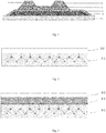
- the structure of a thin film transistor includes: a base substrate 1, a gate electrode 2 arranged on the base substrate 1, a gate insulation layer 3 arranged on a surface of the gate electrode 2, a semiconductor layer 4 arranged on the gate insulation layer 3, and a source electrode 5 and a drain electrode 6 arranged on the semiconductor layer 4.
- the gate insulation layer 3 includes a metal oxide layer 3-1 and a modified layer 3-2 located on a side of the metal oxide layer away from the gate electrode and formed through self-assembling.
- a material of the metal oxide layer having a dielectric constant of 10 or more, and the metal oxide layer has a thickness of less than 200 nm.
- the material of the metal oxide layer may be hafnium oxide, zirconium oxide, titanium oxide, titanium oxide, tantalum oxide, cerium oxide, or gadolinium oxide.
- a material of the metal oxide layer has a dielectric constant of 5 to 10, and the metal oxide layer has a thickness of 5 nm to 50 nm.
- the material of the metal oxide layer may be aluminum oxide.
- the material of the modified layer may be silazane or chlorosilane.
- the modified layer can form a chemical bonding with the metal oxide. It has a modification effect on the metal oxide layer and has high stability. Especially, after the surface of the metal oxide layer is modified by silazane or chlorosilane, an array of the dense and ordered alkyl group can effectively prevent the carrier from tunneling to the gate insulation layer, so that the threshold voltage drift phenomenon can be effectively suppressed.
- the modified layer can have a thickness of 10 nm or less.
- the material of the metal oxide layer is aluminum oxide
- the gate insulation layer composed of an aluminum oxide layer and a modified layer has good dielectric properties, and an array of the dense and ordered alkyl group of the modified layer located on the surface of the aluminum oxide layer can effectively prevent the carrier from tunneling to the gate insulation layer, so that the threshold voltage drift phenomenon can be effectively suppressed.
- the silazane used as the material of the modified layer may be hexamethyldisilazane (HMDS).
- HMDS hexamethyldisilazane
- the gate insulation layer includes an aluminum oxide layer and a modified layer formed of hexamethyldisilazane.
- 3-1 is an aluminum oxide layer and 3-2 is a modified layer formed of hexamethyldisilazane.
- Chlorosilane is shown in formula (II): wherein n is an even number between 8 and 18.
- the gate insulation layer further includes an adhesion layer located between the modified layer and the metal oxide layer.
- the adhesion layer can have a thickness of 10 nm to 20 nm.
- the adhesion layer can improve the bonding strength between the metal oxide layer and the modified layer, and can improve the corrosion resistance.
- the material of the adhesion layer may be polymethylsilsesquioxane (PMSQ).
- PMSQ polymethylsilsesquioxane
- formula (III) wherein R and R' are alkyl or aryl; m is a positive integer and represents the degree of polymerization.
- the gate insulation layer includes an aluminum oxide layer, a polymethylsilsesquioxane layer, and a hexamethyldisilazane layer arranged in order.
- 3-1 is an aluminum oxide layer
- 3-2 is a modified layer formed of hexamethyldisilazane
- 3-3 is an adhesion layer formed of polymethylsilsesquioxane.
- the material of the gate electrode includes aluminum.
- the gate insulation layer is provided with a via hole for exposing the gate electrode, and the semiconductor layer fills the via hole in the gate insulation layer, so that a source electrode and a drain electrode that are subsequently deposited can be prevented from directly contacting the gate electrode.
- the capacitance of the gate insulation layer and the on-state current can be effectively improved by reducing the thickness of the gate insulation layer or by increasing the dielectric constant of the gate insulation layer.
- the capacitance of the gate insulation layer can reach 70 nF/cm 2 to 700 nF/cm2.
- the gate insulation layer includes a metal oxide layer and a modified layer located on a side of the metal oxide layer away from the gate, and these change the material and structure of the gate insulation layer, thereby improving the capacitance of the thin film transistor, obtaining a higher on-state current, and improving charging efficiency.
- the modified layer has a protective effect on the metal oxide layer and can improve the adhesion between the metal oxide layer and the semiconductor layer.
- the preparation method of the gate insulation layer is simple and convenient, and is conducive to extensive application in the process of preparing a thin film transistor. Experimental results show that when the gate insulation layer is used in the thin film transistor of the present disclosure, the capacitance can reach 70 nF/cm 2 to 700 nF/cm 2 .
- the capacitance of the thin film transistor disclosed in the present disclosure is increased by almost two orders of magnitude, and it is easy to operate at a voltage less than 5 volt.
- An embodiment of the present disclosure also provides a method for preparing a thin film transistor, as shown in Fig. 4 , for example, including: providing a base substrate; forming a gate electrode on the base substrate; forming a gate insulation layer: forming a semiconductor layer on the gate insulation layer, an orthogonal projection of the semiconductor layer on the base substrate falling within an orthogonal projection of the gate electrode on the base substrate; and forming a source electrode and a drain electrode on a base substrate on which a semiconductor layer is formed, to obtain a thin film transistor, in which the forming the gate insulating layer includes forming a metal oxide layer on a surface of the gate electrode; and forming a modified layer through self-assembling on a side of the metal oxide layer away from the gate electrode.
- the method for preparing a thin film transistor according to an embodiment of the present disclosure includes, for example, the following steps S1 to S5.
- the base substrate may be a glass substrate or a flexible substrate.
- the material of the gate can be Cu, Ti, Cr, or Al, etc.
- the forming the gate electrode on the base substrate may include depositing a gate metal layer on the base substrate, and patterning the gate metal layer, to obtain a gate electrode.
- the patterning process can be performed in the following manner, but is not limited thereto.
- a layer of photoresist is coated on the gate metal layer, and the photoresist is exposed by using a mask to form a photoresist unreserved region, a photoresist partially reserved region and a photoresist reserved region.
- the photoresist reserved region corresponds to a region in which the pattern of the gate electrode is located
- the photoresist partially reserved region corresponds to a region in which the pattern of the via hole is located
- the photoresist unreserved region corresponds to a region outside of the above pattern
- development processing is performed, so that the photoresist in the photoresist unreserved region is completely removed, and the thickness of the photoresist in the photoresist reserved region remains unchanged
- the gate metal film of the photoresist unreserved region is completely etched away by an etching process, the photoresist in the photoresist partially reserved region is ashed away to form a photoresist pattern for protecting the via hole; and the remaining photo
- the forming the gate insulating layer includes: forming a metal oxide layer on a surface of the gate electrode; and forming a modified layer through self-assembling on a side of the metal oxide layer away from the gate electrode, to obtain a gate insulation layer.
- the material of the metal oxide layer may be a material having a dielectric constant of 10 or more, and the metal oxide layer is formed to have a thickness of less than 200 nm.
- the material of the metal oxide layer may be hafnium oxide, zirconium oxide, titanium oxide, titanium oxide, tantalum oxide, cerium oxide, or gadolinium oxide.
- the material of the metal oxide layer may be a material having a dielectric constant of 5 to 10, and the metal oxide layer is formed to have a thickness of 5 to 50 nm.
- the material of the metal oxide layer may be aluminum oxide.
- the forming the metal oxide layer on the surface of the gate electrode may include forming an aluminum oxide layer on the surface of the gate electrode by oxygen plasma direct oxidation, PECVD, or atomic layer deposition. Depending on the metal used for the gate electrode, different methods are used to form the aluminum oxide layer.
- an aluminum oxide layer is formed on the surface of the gate electrode by oxygen plasma oxidation.
- the forming the aluminum oxide layer on the surface of the gate by oxygen plasma oxidation may alternatively include directly oxidizing the gate electrode in an oxygen plasma environment, to form an aluminum oxide layer on the surface of the gate electrode.
- the aluminum oxide layer may have a thickness of 5 nm to 50 nm.
- the gate electrode is made of aluminum
- the gate insulation layer includes an aluminum oxide layer and a modified layer located on the side of the aluminum oxide layer away from the gate electrode and formed through self-assembling
- the process of forming an aluminum oxide layer on the surface of the gate electrode by oxygen plasma oxidation can be well compatible with the process of preparing the gate electrode.
- a dense aluminum oxide layer is thermally grown with the help of oxygen plasma, thereby eliminating several complicated PECVD steps required by the deposition of the gate insulation layer.
- the aluminum oxide layer and the aluminum gate electrode have a good contact, which can reduce the stress of the aluminum gate electrode.
- the gate electrode may also be a metal other than aluminum.
- an aluminum oxide layer may be formed on the surface of the gate electrode by PECVD or atomic layer deposition.
- the method of forming the aluminum oxide layer on the surface of the gate electrode by atomic layer deposition method includes: treating the gate electrode with trimethylaluminum to adsorb trimethylaluminum on the surface of the gate electrode; removing excess trimethylaluminum by an inert gas, in which the inert gas may be argon; and oxidizing the trimethylaluminum adsorbed on the surface of the gate electrode by oxygen to form an aluminum oxide layer.
- the modified layer is formed to have a thickness of 10 nm or less.
- the material of the modified layer may be silazane or chlorosilane.
- the forming the modified layer on the side of the metal oxide layer away from the gate electrode through self-assembling may include: treating a surface of the metal oxide layer away from the gate electrode with silazane or chlorosilane, to form the modified layer.
- the treating the surface of the metal oxide layer with silazane or chlorosilane can be performed by vapor deposition or solution coating, so that the silazane or chlorosilane can be self-assembled with the metal oxide.
- the silazane may be hexamethyldisilazane.
- the forming the modified layer may include: treating a surface of the metal oxide layer away from the gate electrode with hexamethyldisilazane vapor or a solution containing hexamethyldisilazane, to form the modified layer.
- the gate insulation layer may further include an adhesion layer arranged between the metal oxide layer and the modified layer.
- the forming the gate insulation layer further includes: after forming the metal oxide layer on the gate surface and before forming the modified layer, forming the adhesion layer on a surface of the metal oxide layer away from the gate electrode, in which the forming the modified layer includes forming a modified layer on a surface of the adhesion layer away from the gate electrode.
- the adhesion layer has a thickness of 10 nm to 20 nm.
- the material of the adhesion layer may be polymethylsilsesquioxane
- the forming the gate insulation layer may include: forming a metal oxide layer on the surface of the gate electrode; coating a solution containing polymethylsilsesquioxane on a surface of the metal oxide layer away from the gate electrode and then vacuum drying to form the adhesion layer; performing plasma treatment on the adhesion layer to obtain a hydrophilic surface; and treating the hydrophilic surface with silazane or chlorosilane to form the modified layer.
- the forming the gate insulation layer may include: forming a metal oxide layer on the surface of the gate electrode; coating a solution containing polymethylsilsesquioxane on a surface of the metal oxide layer away from the gate electrode and then vacuum drying to form the adhesion layer; performing plasma treatment on the adhesion layer to obtain a hydrophilic surface; and treating the hydrophilic surface with hexamethyldisilazane vapor or a solution containing hexamethyldisilazane, to form the modified layer.
- the forming the gate insulation layer may include: forming an aluminum oxide layer on a surface of the gate electrode; coating a solution containing polymethylsilsesquioxane on a surface of the aluminum oxide layer away from the gate electrode and then vacuum drying to form the adhesion layer; performing plasma treatment on the adhesion layer to obtain a hydrophilic surface; and treating the hydrophilic surface with hexamethyldisilazane vapor or a solution containing hexamethyldisilazane to form the modified layer.
- the adhesion layer formed of polymethylsilsesquioxane and the modified layer formed of hexamethyldisilazane on the surface of the aluminum oxide layer are sequentially modified by the self-assembly method.
- the method is simple, the reaction efficiency is good, and the layers are tightly combined.
- the forming the gate insulation layer further includes forming a via hole for exposing the gate electrode in the gate insulation layer.
- the semiconductor layer can be made of amorphous silicon (a-Si), low temperature polysilicon (LTPS), indium gallium zinc oxide (IGZO), etc.
- a-Si amorphous silicon
- LTPS low temperature polysilicon
- IGZO indium gallium zinc oxide
- a semiconductor layer may be formed on the gate insulation layer.
- the forming the semiconductor layer may include depositing a semiconductor thin film on the modified layer, to obtain a semiconductor layer after a patterning process.
- a via hole is formed in a gate insulation layer composed of a metal oxide layer and a modified layer, for example, a semiconductor thin film is also deposited at the exposed via hole for exposing the gate electrode and a semiconductor layer is formed after a patterning process, thereby preventing subsequent deposition of the source electrode and the drain electrode in direct contact with the gate electrode.
- the semiconductor layer can have a thickness of 100 nm or more.
- S5 forming a source electrode and a drain electrode on a base substrate on which the semiconductor layer is formed to obtain a thin film transistor.
- the source electrode and the drain electrode may include metals, such as Al, Cu, Ti, and Cr.
- the method for preparing the source electrode and the drain electrode may include depositing a source/drain electrode layer, and forming a source and a drain after a patterning process.
- the source electrode and the drain electrode are arranged on the semiconductor layer to minimize the parasitic capacitance.
- an encapsulation layer can be deposited, and then a thin film transistor is obtained.
- the encapsulation layer can be silicon nitride of 500 nm or more.
- the encapsulation layer, the semiconductor layer, and the gate insulation layer are etched by a dry etching process, to form a via hole at an appropriate position of the gate electrode.
- the encapsulation layer can also be etched by a dry etching process, to form a via hole at an appropriate position on the source electrode.
- An embodiment of the present disclosure also provides a display substrate including the thin film transistor as described above.
- An embodiment of the present disclosure further provides a display device including the display substrate as described above.
- the on-state current is high due to the large capacitance of the thin film transistor, thereby greatly reducing the driving voltage of the gate electrode and the load of the peripheral driving circuit, thereby reducing the power consumption of the display substrate or the display device and achieving a higher energy efficiency ratio.
- An embodiment of the present disclosure further provides a display substrate including the thin film transistor as described above.
- the display substrate may be an LCD or OLED display substrate based on a glass substrate.
- the modified layer and/or the adhesion layer are formed on the metal oxide layer through self-assembly, the high temperature chemical vapor deposition process is avoided, and thus it is suitable for use in organic flexible substrates.
- An embodiment of the present disclosure further provides a display device including the display substrate as described above.
- a method for preparing a thin film transistor includes providing a glass substrate as the base substrate 1.
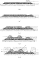
- a gate metal thin film 2' formed of aluminum is deposited on a glass substrate, a layer of photoresist 7 is coated on the gate metal thin film 2', and the photoresist 7 is exposed by using a mask to allow the photoresist 7 to form a photoresist unreserved region, a photoresist partially reserved region, and a photoresist reserved region.
- the photoresist reserved region corresponds to a region where the pattern of the gate electrode 2 is located
- the photoresist partially reserved region corresponds to a region where the via hole is located
- the photoresist unreserved region corresponds to a region outside of the above pattern.
- An exemplary structure is shown in Fig. 5 .
- a development processing is performed, so that the photoresist 7 in the photoresist unreserved region is completely removed, and the thickness of the photoresist 7 in the photoresist reserved region remains unchanged.
- the gate metal thin film 2' of the photoresist unreserved region is completely etched by an etching process.
- the photoresist 7 of the photoresist partially reserved region is ashed away to form a photoresist pattern for protecting the via hole.
- the remaining photoresist 7 is stripped to form the pattern of the gate electrode 2.
- An exemplary structure is shown in Fig. 6 .
- the gate electrode 2 is directly oxidized in an oxygen plasma environment, to form an aluminum oxide layer on the surface of the gate electrode 2.
- the aluminum oxide layer may have a thickness of 5 nm to 50 nm.
- a solution containing polymethylsilsesquioxane is coated on the surface of the aluminum oxide layer away from the gate electrode 2 and then vacuum dried, for example, at 5 to 20 Pa and 80 °C, to form an adhesion layer.
- a plasma treatment is performed on the adhesion layer to obtain a hydrophilic surface, and the hydrophilic surface is treated with hexamethyldisilazane vapor or a solution containing hexamethyldisilazane to form the modified layer.
- the aluminum oxide layer, the adhesion layer, and the modified layer together constitute the gate insulation layer 3.
- An exemplary structure is shown in Fig. 7 .
- a semiconductor thin film is deposited on the glass substrate that has completed the above operations, a layer of photoresist is coated on the semiconductor thin film, and the photoresist is exposed by using a mask to form a photoresist unreserved region and a photoresist reserved region.
- the photoresist reserved region corresponds to a region where the pattern of the semiconductor layer 4 is located, and the photoresist unreserved region corresponds to a region outside of the above pattern.
- the development processing is performed, so that the photoresist in the photoresist unreserved region is completely removed, and the thickness of the photoresist in the photoresist reserved region remains unchanged.
- the semiconductor metal film of the photoresist unreserved region is completely etched away by an etching process, and the remaining photoresist is stripped to form a semiconductor layer 4.
- An exemplary structure is shown in Fig. 8 .
- the source/drain metal layer may be metals such as Cu, Al, Ag, Mo, Cr, Nd, Ni, Mn, Ti, Ta, W, and alloys of these metals.
- the source/drain metal layer may be a single layer structure or a multilayer structure, such as Cu ⁇ Mo, Ti ⁇ Cu ⁇ Ti, and Mo ⁇ Al ⁇ Mo.
- a layer of photoresist is coated on the source/drain metal layer, and the photoresist is exposed by using a mask to form a photoresist unreserved region and a photoresist reserved region.
- the photoresist reserved region corresponds to a region in which the pattern of the source electrode 5/the drain electrode 6 is located, and the photoresist unreserved region corresponds to a region outside of the above pattern.
- the development processing is performed, so that the photoresist in the photoresist unreserved region is completely removed, and the thickness of the photoresist in the photoresist reserved region remains unchanged.
- the source/drain metal layer of the photoresist unreserved region is completely etched away by an etching process, and the remaining photoresist is stripped to form a pattern of the drain electrode and the source electrode.
- An exemplary structure is shown in Fig. 9 .
- the encapsulation layer 8 when the encapsulation layer 8 is deposited, the encapsulation layer 8, the semiconductor layer 4, and the gate insulation layer 3 are etched by a dry etching process, to form a via hole at an appropriate position of the gate electrode 2. At the same time, the encapsulation layer 8 is etched by a dry etching process to form a via hole at an appropriate position of the source electrode 5, thereby obtaining a thin film transistor.
- An exemplary structure is shown in Fig. 10 .
- a method for preparing a thin film transistor includes the following steps.
- a glass substrate is provided.
- An aluminum thin film is deposited on the glass substrate, a layer of photoresist is coated on the aluminum thin film, and the photoresist is exposed by using a mask to allow the photoresist to form a photoresist unreserved region, a photoresist partially reserved region, and a photoresist reserved region.
- the photoresist reserved region corresponds to a region where the pattern of the gate electrode is located
- the photoresist partially reserved region corresponds to a region where the via hole is located
- the photoresist unreserved region corresponds to a region outside of the above pattern.
- a development processing is performed, so that the photoresist in the photoresist unreserved region is completely removed, and the thickness of the photoresist in the photoresist reserved region remains unchanged.
- the aluminum thin film of the photoresist unreserved region is completely etched by an etching process, and the photoresist of the photoresist partially reserved region is ashed to form a photoresist pattern for protecting the via hole; and the remaining photoresist is stripped to form a pattern of the gate electrode.
- the gate electrode is directly oxidized in an oxygen plasma environment, to form an aluminum oxide layer on the surface of the gate electrode, and the aluminum oxide layer can have a thickness of 5 nm to 50 nm.
- the surface of the aluminum oxide layer away from the gate is treated with hexamethyldisilazane vapor or a solution containing hexamethyldisilazane to form the modified layer.
- the aluminum oxide layer, and the modified layer together constitute the gate insulation layer.
- a semiconductor thin film is deposited on the glass substrate that has completed the above operations, a layer of photoresist is coated on the semiconductor thin film, and the photoresist is exposed by using a mask to form a photoresist unreserved region and a photoresist reserved region.
- the photoresist reserved region corresponds to a region where the pattern of the semiconductor layer is located, and the photoresist unreserved region corresponds to a region outside of the above pattern.
- a development processing is performed, so that the photoresist in the photoresist unreserved region is completely removed, and the thickness of the photoresist in the photoresist reserved region remains unchanged.
- the semiconductor metal film of the photoresist unreserved region is completely etched away by an etching process, and the remaining photoresist is stripped to form a semiconductor layer.
- the source/drain metal layer may be metals such as Cu, Al, Ag, Mo, Cr, Nd, Ni, Mn, Ti, Ta, W, and alloys of these metals.
- the source/drain metal layer may be a single layer structure or a multilayer structure, such as Cu ⁇ Mo, Ti ⁇ Cu ⁇ Ti, and Mo ⁇ Al ⁇ Mo.
- a layer of photoresist is coated on the source/drain metal layer, and the photoresist is exposed by using a mask to form a photoresist unreserved region and a photoresist reserved region.
- the photoresist reserved region corresponds to a region in which the pattern of the source/drain electrode is located, and the photoresist unreserved region corresponds to a region outside of the above pattern.
- a development processing is performed, so that the photoresist in the photoresist unreserved region is completely removed, and the thickness of the photoresist in the photoresist reserved region remains unchanged.
- the source/drain metal layer of the photoresist unreserved region is completely etched away by an etching process, and the remaining photoresist is stripped to form a pattern of the drain electrode and the source electrode.
- the encapsulation layer When the encapsulation layer is deposited, the encapsulation layer, the semiconductor layer, and the gate insulation layer are etched by a dry etching process, to form a via hole at an appropriate position for exposing the gate electrode. At the same time, the encapsulation layer is etched by a dry etching process to form a via hole at an appropriate position of the source electrode, thereby obtaining a thin film transistor.
Landscapes
- Thin Film Transistor (AREA)
- Physics & Mathematics (AREA)
- Engineering & Computer Science (AREA)
- Plasma & Fusion (AREA)
Applications Claiming Priority (2)
| Application Number | Priority Date | Filing Date | Title |
|---|---|---|---|
| CN201810101958.8A CN110112219B (zh) | 2018-02-01 | 2018-02-01 | 一种薄膜晶体管、其制备方法、显示基板及显示装置 |
| PCT/CN2018/110637 WO2019148892A1 (fr) | 2018-02-01 | 2018-10-17 | Transistor à couches minces et son procédé de fabrication, substrat d'affichage et dispositif d'affichage |
Publications (2)
| Publication Number | Publication Date |
|---|---|
| EP3748687A1 true EP3748687A1 (fr) | 2020-12-09 |
| EP3748687A4 EP3748687A4 (fr) | 2021-10-27 |
Family
ID=67479574
Family Applications (1)
| Application Number | Title | Priority Date | Filing Date |
|---|---|---|---|
| EP18903206.3A Withdrawn EP3748687A4 (fr) | 2018-02-01 | 2018-10-17 | Transistor à couches minces et son procédé de fabrication, substrat d'affichage et dispositif d'affichage |
Country Status (4)
| Country | Link |
|---|---|
| US (1) | US11355614B2 (fr) |
| EP (1) | EP3748687A4 (fr) |
| CN (1) | CN110112219B (fr) |
| WO (1) | WO2019148892A1 (fr) |
Families Citing this family (1)
| Publication number | Priority date | Publication date | Assignee | Title |
|---|---|---|---|---|
| CN114664950B (zh) * | 2022-03-25 | 2025-06-03 | 汕头超声显示器技术有限公司 | 一种改进绝缘层的氧化物半导体的薄膜晶体管 |
Family Cites Families (13)
| Publication number | Priority date | Publication date | Assignee | Title |
|---|---|---|---|---|
| US20060063014A1 (en) * | 2004-07-12 | 2006-03-23 | Debbie Forray | Polyalkylsilsesquioxane-filled adhesive compositions and methods for use thereof |
| KR100788758B1 (ko) * | 2006-02-06 | 2007-12-26 | 양재우 | 저전압 유기 박막 트랜지스터 및 그 제조 방법 |
| US20080135891A1 (en) | 2006-12-08 | 2008-06-12 | Palo Alto Research Center, Incorporated | Transistor Device Formed on a Flexible Substrate Including Anodized Gate Dielectric |
| GB2462845B (en) | 2008-08-21 | 2011-07-27 | Cambridge Display Tech Ltd | Organic electronic devices and methods of making the same using solution processing techniques |
| US8309954B2 (en) | 2009-05-12 | 2012-11-13 | Toppan Printing Co., Ltd. | Insulating thin film, formation solution for insulating thin film, field-effect transistor, method for manufacturing the same and image display unit |
| KR101781549B1 (ko) * | 2010-12-02 | 2017-09-27 | 삼성디스플레이 주식회사 | 표시 기판 및 이의 제조 방법 |
| CN102881828A (zh) * | 2012-10-10 | 2013-01-16 | 上海交通大学 | 一种短沟道有机薄膜晶体管的制备方法 |
| JP6004092B2 (ja) * | 2013-04-18 | 2016-10-05 | 富士電機株式会社 | 積層体および積層体の製造方法 |
| CN103413832B (zh) * | 2013-07-08 | 2016-01-20 | 复旦大学 | 一种金属氧化物薄膜晶体管及其制备方法 |
| CN103700710B (zh) * | 2013-12-30 | 2018-07-13 | Tcl集团股份有限公司 | Igzo薄膜晶体管及其制备方法 |
| CN104332559A (zh) * | 2014-11-26 | 2015-02-04 | 中国科学院微电子研究所 | 一种低操作电压有机场效应晶体管及其制备方法 |
| CN104730137A (zh) | 2015-03-27 | 2015-06-24 | 中国科学院上海微系统与信息技术研究所 | 基于超薄绝缘层soi上的mosfet背栅生物传感器及其制备方法 |
| WO2018084804A1 (fr) * | 2016-11-03 | 2018-05-11 | Agency For Science, Technology And Research | Dépôt autocatalytique de nickel de caoutchouc de silicone |
-
2018
- 2018-02-01 CN CN201810101958.8A patent/CN110112219B/zh not_active Expired - Fee Related
- 2018-10-17 EP EP18903206.3A patent/EP3748687A4/fr not_active Withdrawn
- 2018-10-17 US US16/760,410 patent/US11355614B2/en active Active
- 2018-10-17 WO PCT/CN2018/110637 patent/WO2019148892A1/fr not_active Ceased
Also Published As
| Publication number | Publication date |
|---|---|
| WO2019148892A1 (fr) | 2019-08-08 |
| CN110112219B (zh) | 2021-02-09 |
| US20200343356A1 (en) | 2020-10-29 |
| US11355614B2 (en) | 2022-06-07 |
| CN110112219A (zh) | 2019-08-09 |
| EP3748687A4 (fr) | 2021-10-27 |
Similar Documents
| Publication | Publication Date | Title |
|---|---|---|
| US9355838B2 (en) | Oxide TFT and manufacturing method thereof | |
| TW201222676A (en) | Thin film transistors and methods for manufacturing the same | |
| CN104241392B (zh) | 一种薄膜晶体管及其制备方法、显示基板和显示设备 | |
| TW200952181A (en) | Process to make metal oxide thin film transistor array with etch stopping layer | |
| CN110098261A (zh) | 一种薄膜晶体管及其制作方法、显示基板、面板、装置 | |
| TW200404824A (en) | Organic gate insulating film and organic thin film transistor using the same | |
| CN104272461B (zh) | 用于增加金属氧化物半导体层的电导率的方法 | |
| CN102668099A (zh) | 挠性半导体装置及其制造方法、以及图像显示装置 | |
| US9786791B2 (en) | Thin film transistor, array substrate and method of manufacturing the same | |
| CN104867985A (zh) | 一种薄膜晶体管、其制备方法、阵列基板及显示装置 | |
| CN103715272A (zh) | 金属氧化物薄膜晶体管及其制备方法 | |
| TWI508183B (zh) | 形成含氧半導體薄膜電晶體之方法 | |
| CN103730373B (zh) | 一种半导体器件的制备方法及半导体器件 | |
| CN102738243B (zh) | 晶体管、阵列基板及其制造方法、液晶面板和显示装置 | |
| EP3291304B1 (fr) | Couche mince de semi-conducteur à oxyde, transistor à couches minces, et procédé de préparation et dispositif | |
| CN104505405A (zh) | 薄膜晶体管及制备方法、阵列基板及制备方法、显示装置 | |
| US11355614B2 (en) | Thin film transistor, method for preparing the same, display substrate and display device | |
| US9123815B1 (en) | VTFTs including offset electrodes | |
| US10985320B2 (en) | Organic transistor and manufacturing method thereof, array substrate, display device | |
| WO2015134092A1 (fr) | Vtft comprenant des électrodes se chevauchant | |
| WO2014173146A1 (fr) | Transistor à couche mince, son procédé de fabrication, substrat de matrice et appareil d'affichage | |
| CN208548341U (zh) | 石墨烯晶体管电路装置 | |
| EP2219244B1 (fr) | Agent de modification de surface, structure stratifiée et transistor l'incluant et procédé de fabrication de la structure stratifiée | |
| KR101876011B1 (ko) | 산화물 박막 트랜지스터 및 그 제조방법 | |
| CN104319285A (zh) | 一种薄膜晶体管及其制备方法、阵列基板 |
Legal Events
| Date | Code | Title | Description |
|---|---|---|---|
| STAA | Information on the status of an ep patent application or granted ep patent |
Free format text: STATUS: THE INTERNATIONAL PUBLICATION HAS BEEN MADE |
|
| PUAI | Public reference made under article 153(3) epc to a published international application that has entered the european phase |
Free format text: ORIGINAL CODE: 0009012 |
|
| STAA | Information on the status of an ep patent application or granted ep patent |
Free format text: STATUS: REQUEST FOR EXAMINATION WAS MADE |
|
| 17P | Request for examination filed |
Effective date: 20200608 |
|
| AK | Designated contracting states |
Kind code of ref document: A1 Designated state(s): AL AT BE BG CH CY CZ DE DK EE ES FI FR GB GR HR HU IE IS IT LI LT LU LV MC MK MT NL NO PL PT RO RS SE SI SK SM TR |
|
| AX | Request for extension of the european patent |
Extension state: BA ME |
|
| DAV | Request for validation of the european patent (deleted) | ||
| DAX | Request for extension of the european patent (deleted) | ||
| A4 | Supplementary search report drawn up and despatched |
Effective date: 20210923 |
|
| RIC1 | Information provided on ipc code assigned before grant |
Ipc: H01L 29/49 20060101ALI20210917BHEP Ipc: H01L 21/02 20060101ALI20210917BHEP Ipc: H01L 21/336 20060101ALI20210917BHEP Ipc: H01L 29/51 20060101ALI20210917BHEP Ipc: H01L 29/786 20060101AFI20210917BHEP |
|
| STAA | Information on the status of an ep patent application or granted ep patent |
Free format text: STATUS: THE APPLICATION HAS BEEN WITHDRAWN |
|
| 18W | Application withdrawn |
Effective date: 20220928 |