EP3748700A1 - Leuchtdiodenchip und herstellungsverfahren dafür - Google Patents
Leuchtdiodenchip und herstellungsverfahren dafür Download PDFInfo
- Publication number
- EP3748700A1 EP3748700A1 EP18908112.8A EP18908112A EP3748700A1 EP 3748700 A1 EP3748700 A1 EP 3748700A1 EP 18908112 A EP18908112 A EP 18908112A EP 3748700 A1 EP3748700 A1 EP 3748700A1
- Authority
- EP
- European Patent Office
- Prior art keywords
- light
- sub
- pixel
- quantum well
- region
- Prior art date
- Legal status (The legal status is an assumption and is not a legal conclusion. Google has not performed a legal analysis and makes no representation as to the accuracy of the status listed.)
- Granted
Links
Images


Classifications
-
- H—ELECTRICITY
- H10—SEMICONDUCTOR DEVICES; ELECTRIC SOLID-STATE DEVICES NOT OTHERWISE PROVIDED FOR
- H10H—INORGANIC LIGHT-EMITTING SEMICONDUCTOR DEVICES HAVING POTENTIAL BARRIERS
- H10H20/00—Individual inorganic light-emitting semiconductor devices having potential barriers, e.g. light-emitting diodes [LED]
- H10H20/80—Constructional details
- H10H20/81—Bodies
- H10H20/822—Materials of the light-emitting regions
- H10H20/824—Materials of the light-emitting regions comprising only Group III-V materials, e.g. GaP
- H10H20/825—Materials of the light-emitting regions comprising only Group III-V materials, e.g. GaP containing nitrogen, e.g. GaN
-
- H—ELECTRICITY
- H10—SEMICONDUCTOR DEVICES; ELECTRIC SOLID-STATE DEVICES NOT OTHERWISE PROVIDED FOR
- H10H—INORGANIC LIGHT-EMITTING SEMICONDUCTOR DEVICES HAVING POTENTIAL BARRIERS
- H10H29/00—Integrated devices, or assemblies of multiple devices, comprising at least one light-emitting semiconductor element covered by group H10H20/00
- H10H29/10—Integrated devices comprising at least one light-emitting semiconductor component covered by group H10H20/00
- H10H29/14—Integrated devices comprising at least one light-emitting semiconductor component covered by group H10H20/00 comprising multiple light-emitting semiconductor components
- H10H29/142—Two-dimensional arrangements, e.g. asymmetric LED layout
-
- H—ELECTRICITY
- H10—SEMICONDUCTOR DEVICES; ELECTRIC SOLID-STATE DEVICES NOT OTHERWISE PROVIDED FOR
- H10H—INORGANIC LIGHT-EMITTING SEMICONDUCTOR DEVICES HAVING POTENTIAL BARRIERS
- H10H20/00—Individual inorganic light-emitting semiconductor devices having potential barriers, e.g. light-emitting diodes [LED]
- H10H20/01—Manufacture or treatment
- H10H20/011—Manufacture or treatment of bodies, e.g. forming semiconductor layers
- H10H20/013—Manufacture or treatment of bodies, e.g. forming semiconductor layers having light-emitting regions comprising only Group III-V materials
- H10H20/0137—Manufacture or treatment of bodies, e.g. forming semiconductor layers having light-emitting regions comprising only Group III-V materials the light-emitting regions comprising nitride materials
-
- H—ELECTRICITY
- H10—SEMICONDUCTOR DEVICES; ELECTRIC SOLID-STATE DEVICES NOT OTHERWISE PROVIDED FOR
- H10H—INORGANIC LIGHT-EMITTING SEMICONDUCTOR DEVICES HAVING POTENTIAL BARRIERS
- H10H20/00—Individual inorganic light-emitting semiconductor devices having potential barriers, e.g. light-emitting diodes [LED]
- H10H20/01—Manufacture or treatment
- H10H20/011—Manufacture or treatment of bodies, e.g. forming semiconductor layers
- H10H20/018—Bonding of wafers
-
- H—ELECTRICITY
- H10—SEMICONDUCTOR DEVICES; ELECTRIC SOLID-STATE DEVICES NOT OTHERWISE PROVIDED FOR
- H10H—INORGANIC LIGHT-EMITTING SEMICONDUCTOR DEVICES HAVING POTENTIAL BARRIERS
- H10H20/00—Individual inorganic light-emitting semiconductor devices having potential barriers, e.g. light-emitting diodes [LED]
- H10H20/80—Constructional details
- H10H20/81—Bodies
- H10H20/811—Bodies having quantum effect structures or superlattices, e.g. tunnel junctions
- H10H20/812—Bodies having quantum effect structures or superlattices, e.g. tunnel junctions within the light-emitting regions, e.g. having quantum confinement structures
-
- H—ELECTRICITY
- H10—SEMICONDUCTOR DEVICES; ELECTRIC SOLID-STATE DEVICES NOT OTHERWISE PROVIDED FOR
- H10H—INORGANIC LIGHT-EMITTING SEMICONDUCTOR DEVICES HAVING POTENTIAL BARRIERS
- H10H20/00—Individual inorganic light-emitting semiconductor devices having potential barriers, e.g. light-emitting diodes [LED]
- H10H20/80—Constructional details
- H10H20/81—Bodies
- H10H20/815—Bodies having stress relaxation structures, e.g. buffer layers
-
- H—ELECTRICITY
- H10—SEMICONDUCTOR DEVICES; ELECTRIC SOLID-STATE DEVICES NOT OTHERWISE PROVIDED FOR
- H10H—INORGANIC LIGHT-EMITTING SEMICONDUCTOR DEVICES HAVING POTENTIAL BARRIERS
- H10H20/00—Individual inorganic light-emitting semiconductor devices having potential barriers, e.g. light-emitting diodes [LED]
- H10H20/80—Constructional details
- H10H20/83—Electrodes
- H10H20/831—Electrodes characterised by their shape
- H10H20/8312—Electrodes characterised by their shape extending at least partially through the bodies
-
- H—ELECTRICITY
- H10—SEMICONDUCTOR DEVICES; ELECTRIC SOLID-STATE DEVICES NOT OTHERWISE PROVIDED FOR
- H10H—INORGANIC LIGHT-EMITTING SEMICONDUCTOR DEVICES HAVING POTENTIAL BARRIERS
- H10H29/00—Integrated devices, or assemblies of multiple devices, comprising at least one light-emitting semiconductor element covered by group H10H20/00
- H10H29/01—Manufacture or treatment
- H10H29/011—Manufacture or treatment of integrated devices comprising at least one light-emitting semiconductor component covered by group H10H20/00
-
- H—ELECTRICITY
- H10—SEMICONDUCTOR DEVICES; ELECTRIC SOLID-STATE DEVICES NOT OTHERWISE PROVIDED FOR
- H10H—INORGANIC LIGHT-EMITTING SEMICONDUCTOR DEVICES HAVING POTENTIAL BARRIERS
- H10H29/00—Integrated devices, or assemblies of multiple devices, comprising at least one light-emitting semiconductor element covered by group H10H20/00
- H10H29/01—Manufacture or treatment
- H10H29/012—Manufacture or treatment of active-matrix LED displays
-
- H—ELECTRICITY
- H10—SEMICONDUCTOR DEVICES; ELECTRIC SOLID-STATE DEVICES NOT OTHERWISE PROVIDED FOR
- H10H—INORGANIC LIGHT-EMITTING SEMICONDUCTOR DEVICES HAVING POTENTIAL BARRIERS
- H10H29/00—Integrated devices, or assemblies of multiple devices, comprising at least one light-emitting semiconductor element covered by group H10H20/00
- H10H29/01—Manufacture or treatment
- H10H29/036—Manufacture or treatment of packages
- H10H29/0361—Manufacture or treatment of packages of wavelength conversion means
-
- H—ELECTRICITY
- H10—SEMICONDUCTOR DEVICES; ELECTRIC SOLID-STATE DEVICES NOT OTHERWISE PROVIDED FOR
- H10H—INORGANIC LIGHT-EMITTING SEMICONDUCTOR DEVICES HAVING POTENTIAL BARRIERS
- H10H29/00—Integrated devices, or assemblies of multiple devices, comprising at least one light-emitting semiconductor element covered by group H10H20/00
- H10H29/80—Constructional details
- H10H29/85—Packages
- H10H29/851—Wavelength conversion means
- H10H29/8511—Wavelength conversion means characterised by their material, e.g. binder
- H10H29/8512—Wavelength conversion materials
-
- H—ELECTRICITY
- H10—SEMICONDUCTOR DEVICES; ELECTRIC SOLID-STATE DEVICES NOT OTHERWISE PROVIDED FOR
- H10H—INORGANIC LIGHT-EMITTING SEMICONDUCTOR DEVICES HAVING POTENTIAL BARRIERS
- H10H29/00—Integrated devices, or assemblies of multiple devices, comprising at least one light-emitting semiconductor element covered by group H10H20/00
- H10H29/80—Constructional details
- H10H29/962—Stacked configurations of light-emitting semiconductor components or devices, the components or devices emitting at different wavelengths
-
- H—ELECTRICITY
- H10—SEMICONDUCTOR DEVICES; ELECTRIC SOLID-STATE DEVICES NOT OTHERWISE PROVIDED FOR
- H10H—INORGANIC LIGHT-EMITTING SEMICONDUCTOR DEVICES HAVING POTENTIAL BARRIERS
- H10H20/00—Individual inorganic light-emitting semiconductor devices having potential barriers, e.g. light-emitting diodes [LED]
- H10H20/01—Manufacture or treatment
- H10H20/032—Manufacture or treatment of electrodes
-
- H—ELECTRICITY
- H10—SEMICONDUCTOR DEVICES; ELECTRIC SOLID-STATE DEVICES NOT OTHERWISE PROVIDED FOR
- H10H—INORGANIC LIGHT-EMITTING SEMICONDUCTOR DEVICES HAVING POTENTIAL BARRIERS
- H10H20/00—Individual inorganic light-emitting semiconductor devices having potential barriers, e.g. light-emitting diodes [LED]
- H10H20/01—Manufacture or treatment
- H10H20/036—Manufacture or treatment of packages
- H10H20/0364—Manufacture or treatment of packages of interconnections
-
- H—ELECTRICITY
- H10—SEMICONDUCTOR DEVICES; ELECTRIC SOLID-STATE DEVICES NOT OTHERWISE PROVIDED FOR
- H10H—INORGANIC LIGHT-EMITTING SEMICONDUCTOR DEVICES HAVING POTENTIAL BARRIERS
- H10H20/00—Individual inorganic light-emitting semiconductor devices having potential barriers, e.g. light-emitting diodes [LED]
- H10H20/80—Constructional details
- H10H20/81—Bodies
- H10H20/813—Bodies having a plurality of light-emitting regions, e.g. multi-junction LEDs or light-emitting devices having photoluminescent regions within the bodies
-
- H—ELECTRICITY
- H10—SEMICONDUCTOR DEVICES; ELECTRIC SOLID-STATE DEVICES NOT OTHERWISE PROVIDED FOR
- H10H—INORGANIC LIGHT-EMITTING SEMICONDUCTOR DEVICES HAVING POTENTIAL BARRIERS
- H10H29/00—Integrated devices, or assemblies of multiple devices, comprising at least one light-emitting semiconductor element covered by group H10H20/00
- H10H29/01—Manufacture or treatment
- H10H29/032—Manufacture or treatment of electrodes
-
- H—ELECTRICITY
- H10—SEMICONDUCTOR DEVICES; ELECTRIC SOLID-STATE DEVICES NOT OTHERWISE PROVIDED FOR
- H10H—INORGANIC LIGHT-EMITTING SEMICONDUCTOR DEVICES HAVING POTENTIAL BARRIERS
- H10H29/00—Integrated devices, or assemblies of multiple devices, comprising at least one light-emitting semiconductor element covered by group H10H20/00
- H10H29/01—Manufacture or treatment
- H10H29/036—Manufacture or treatment of packages
- H10H29/0364—Manufacture or treatment of packages of interconnections
-
- H—ELECTRICITY
- H10—SEMICONDUCTOR DEVICES; ELECTRIC SOLID-STATE DEVICES NOT OTHERWISE PROVIDED FOR
- H10H—INORGANIC LIGHT-EMITTING SEMICONDUCTOR DEVICES HAVING POTENTIAL BARRIERS
- H10H29/00—Integrated devices, or assemblies of multiple devices, comprising at least one light-emitting semiconductor element covered by group H10H20/00
- H10H29/30—Active-matrix LED displays
- H10H29/34—Active-matrix LED displays characterised by the geometry or arrangement of subpixels within a pixel, e.g. relative disposition of the RGB subpixels
-
- H—ELECTRICITY
- H10—SEMICONDUCTOR DEVICES; ELECTRIC SOLID-STATE DEVICES NOT OTHERWISE PROVIDED FOR
- H10H—INORGANIC LIGHT-EMITTING SEMICONDUCTOR DEVICES HAVING POTENTIAL BARRIERS
- H10H29/00—Integrated devices, or assemblies of multiple devices, comprising at least one light-emitting semiconductor element covered by group H10H20/00
- H10H29/30—Active-matrix LED displays
- H10H29/49—Interconnections, e.g. wiring lines or terminals
-
- H—ELECTRICITY
- H10—SEMICONDUCTOR DEVICES; ELECTRIC SOLID-STATE DEVICES NOT OTHERWISE PROVIDED FOR
- H10H—INORGANIC LIGHT-EMITTING SEMICONDUCTOR DEVICES HAVING POTENTIAL BARRIERS
- H10H29/00—Integrated devices, or assemblies of multiple devices, comprising at least one light-emitting semiconductor element covered by group H10H20/00
- H10H29/80—Constructional details
- H10H29/832—Electrodes
- H10H29/8321—Electrodes characterised by their shape
Definitions
- This application relates to the field of semiconductor technologies, and in particular, to a light-emitting diode chip and a preparation method therefor.
- GaN gallium nitride-based light-emitting diode
- LED light-emitting diode
- micro projection display head-mounted display
- augmented reality augmented reality
- virtual reality virtual reality
- wearable display due to advantages such as a long service life, high stability, and low power consumption.
- a size of a GaN-based LED chip may be controlled in a micron dimension. If the GaN-based LED chip in the micron dimension is used as a display pixel, a light and thin display system with high resolution and low power consumption may be implemented.
- Embodiments of this application provide an LED chip and a preparation method therefor, to implement full-color display.
- an embodiment of this application provides a light-emitting diode LED chip.
- the LED chip includes:
- the LED chip may emit blue light and green light by using the other two sub-pixel structures other than the first sub-pixel structure in the three sub-pixel structures.
- the red-light colloidal quantum dot structure may be used for coating in the region corresponding to the first sub-pixel structure that includes the blue-light quantum well structure and the green-light quantum well structure. In this way, blue light and green light are absorbed and then converted into red light by using the red-light colloidal quantum dot structure, and the LED chip emits red light. Therefore, full-color display can be implemented by using the LED chip provided in the first aspect.
- the N-type GaN doping layer may be a GaN layer doped with silicon
- the P-type GaN doping layer may be a GaN layer doped with magnesium
- a shape of a pixel may be a circle or a square. Therefore, the three sub-pixel regions may all be circular regions, or may all be square regions.
- a size of the sub-pixel region may be set based on different requirements for the LED chip. This is not specifically limited in this embodiment of this application. For example, a diameter of a circular region may be 5 ⁇ m to 50 ⁇ m.
- the blue-light quantum well structure includes N blue-light quantum well layers, and N+1 isolation layers that are used to isolate the N blue-light quantum well layers and that are alternately formed with the N blue-light quantum well layers, where N ⁇ 1.
- the blue-light quantum well structure is formed by alternately growing the isolation layer and the blue-light quantum well layer.
- the blue-light quantum well structure may be formed through three to five cycles of material growth processes.
- the blue-light quantum well structure may include two blue-light quantum well layers and three isolation layers that are alternately formed with the two blue-light quantum well layers.
- the blue-light quantum well layer may be a GaN layer doped with indium.
- the green-light quantum well structure includes M green-light quantum well layers, and M+1 isolation layers that are used to isolate the M green-light quantum well layers and that are alternately formed with the M green-light quantum well layers, where M ⁇ 1.
- the green-light quantum well structure is formed by alternately growing the isolation layer and the green-light quantum well layer.
- the green-light quantum well structure may be formed through three to five cycles of material growth processes.
- the green-light quantum well structure may include two green-light quantum well layers and three isolation layers that are alternately formed with the two green-light quantum well layers.
- the green-light quantum well layer may be a GaN layer doped with indium. A proportion of indium doped in the green-light quantum well layer is different from a proportion of indium doped in the blue-light quantum well layer.
- the LED chip may further include: a red light filter disposed on the red-light colloidal quantum dot structure; a blue light filter disposed in a region that corresponds to a second sub-pixel region in the three sub-pixel regions and that is at the second surface of the N-type GaN doping layer; and a green light filter disposed in a region that corresponds to a third sub-pixel region in the three sub-pixel regions and that is at the second surface of the N-type GaN doping layer.
- the red light filter disposed on red-light colloidal quantum dots can be used to filter out color light (for example, blue light and green light) other than red light in the first sub-pixel region.
- the blue light filter disposed in the region corresponding to the second sub-pixel region can be used to filter out color light (for example, green light) other than blue light in the second sub-pixel region.
- the green light filter disposed in the region corresponding to the third sub-pixel region can be used to filter out color light (for example, blue light) other than green light in the third sub-pixel region.
- the LED chip further includes a drive circuit connected to the three P-type contact electrodes and the N-type contact electrode.
- the drive circuit may control luminous intensity of each sub-pixel structure by using a pulse-width modulation technology, so that blue light, green light, and red light emitted by all the sub-pixel structures in the LED chip have same color brightness.
- the LED chip provided in the first aspect When the LED chip provided in the first aspect is prepared, materials need to be grown on a substrate and a buffer layer. After the material growth is completed, cleavage may be performed on the substrate and the buffer layer because functions of the substrate and the buffer layer have been completed. Certainly, because the substrate and the buffer layer do not affect light-emitting display of the LED chip, cleavage may not be performed on the substrate and the buffer layer.
- the LED chip further includes: a buffer layer and a substrate that are formed at the second surface of the N-type GaN doping layer, where the buffer layer is adjacent to the N-type GaN doping layer, and the substrate is adjacent to the buffer layer and the red-light colloidal quantum dot structure.
- an embodiment of this application provides a preparation method for an LED chip.
- the method includes the following steps:
- the method further includes: respectively disposing at least one red light filter on the at least one red-light colloidal quantum dot structure; respectively disposing at least one blue light filter in a region that is at the second surface of the substrate and that corresponds to at least one second sub-pixel region in the plurality of sub-pixel regions that is used to emit blue light; and respectively disposing at least one green light filter in a region that is at the second surface of the substrate and that corresponds to at least one third sub-pixel region in the plurality of sub-pixel regions that is used to emit green light.
- the method further includes: connecting a drive circuit to the plurality of P-type contact electrodes and the N-type contact electrode through alignment by using a metal solder ball.
- cleavage may be further performed between the LED chip and each of the substrate and the buffer layer in a laser radiation manner.
- the respectively using at least one red-light colloidal quantum dot structure for coating in a region that is at a second surface of the substrate and that corresponds to at least one first sub-pixel region in the plurality of sub-pixel regions that is used to emit red light may be specifically implemented in the following manner: respectively using the at least one red-light colloidal quantum dot structure for coating in the region that is at the surface of the N-type GaN doping layer adjacent to the buffer layer and that corresponds to the at least one first sub-pixel region.
- the performing etching on the second sample based on the mask pattern, protecting structures in the plurality of sub-pixel regions, and exposing the N-type GaN doping layer in the remaining region other than the plurality of sub-pixel regions in the mask pattern may be specifically implemented in the following manner: passivating and protecting a side surface of the LED chip and the plurality of sub-pixel regions; and performing etching on the remaining region by using inductively coupled plasma ICP or through reactive ion etching RIE, so that the N-type GaN doping layer in the remaining region is exposed.
- the respectively forming a plurality of P-type contact electrodes in the plurality of sub-pixel regions, and forming an N-type contact electrode in the remaining region may be specifically implemented in the following manner: evaporating and depositing a gold-nickel alloy by using an electron beam, and respectively forming the plurality of P-type contact electrodes in the plurality of sub-pixel regions after annealing at 200°C to 500°C; and sputtering indium tin oxide ITO or graphite in the remaining region, to form the N-type contact electrode.
- an embodiment of this application provides a light-emitting diode LED chip.
- the LED chip includes:
- the LED chip can emit blue light by using the second sub-pixel structure; and because the third sub-pixel structure in the three sub-pixel structures includes the green-light quantum well structure, the LED chip can emit green light by using the third sub-pixel structure.
- the red-light colloidal quantum dot structure may be used for coating in the region corresponding to the first sub-pixel structure that includes the blue-light quantum well structure or the green-light quantum well structure. In this way, blue light or green light is absorbed and then converted into red light by using the red-light colloidal quantum dot structure, and the LED chip emits red light. Therefore, full-color display can be implemented by using the LED chip provided in the third aspect.
- the N-type GaN doping layer may be a GaN layer doped with silicon; and the P-type GaN doping layer in the first sub-pixel structure, the P-type GaN doping layer in the second sub-pixel structure, and the P-type GaN doping layer in the third sub-pixel structure each may be a GaN layer doped with magnesium.
- a shape of a pixel may be a circle or a square. Therefore, the three sub-pixel regions may all be circular regions, or may all be square regions.
- a size of the sub-pixel region may be set based on different requirements for the LED chip. This is not specifically limited in this embodiment of this application. For example, a diameter of a circular region may be 5 ⁇ m to 50 ⁇ m.
- the blue-light quantum well structure in the second sub-pixel structure includes N blue-light quantum well layers, and N+1 isolation layers that are used to isolate the N blue-light quantum well layers and that are alternately formed with the N blue-light quantum well layers, where N ⁇ 1.
- the blue-light quantum well structure in the second sub-pixel structure is formed by alternately growing the isolation layer and the blue-light quantum well layer.
- the blue-light quantum well structure in the second sub-pixel structure may be formed through three to five cycles of material growth processes.
- the blue-light quantum well structure in the second sub-pixel structure may include two blue-light quantum well layers and three isolation layers that are alternately formed with the two blue-light quantum well layers.
- the blue-light quantum well layer in the second sub-pixel structure may be a GaN layer doped with indium.
- a structure of the blue-light quantum well structure in the first sub-pixel structure may be the same as that of the blue-light quantum well structure in the second sub-pixel structure.
- the green-light quantum well structure in the third sub-pixel structure includes M green-light quantum well layers, and M+1 isolation layers that are used to isolate the M green-light quantum well layers and that are alternately formed with the M green-light quantum well layers, where M ⁇ 1.
- the green-light quantum well structure in the third sub-pixel structure is formed by alternately growing the isolation layer and the green-light quantum well layer.
- the green-light quantum well structure in the third sub-pixel structure may be formed through three to five cycles of material growth processes.
- the green-light quantum well structure in the third sub-pixel structure may include two green-light quantum well layers and three isolation layers that are alternately formed with the two green-light quantum well layers.
- the green-light quantum well layer in the third sub-pixel structure may be a GaN layer doped with indium.
- a proportion of indium doped in the green-light quantum well layer in the third sub-pixel structure is different from a proportion of indium doped in the blue-light quantum well layer in the second sub-pixel structure.
- a structure of the green-light quantum well structure in the first sub-pixel structure may be the same as that of the green-light quantum well structure in the third sub-pixel structure.
- the LED chip may further include: a red light filter disposed on the red-light colloidal quantum dot structure; a blue light filter disposed in a region that corresponds to the second sub-pixel region and that is at the second surface of the N-type GaN doping layer; and a green light filter disposed in a region that corresponds to the third sub-pixel region and that is at the second surface of the N-type GaN doping layer.
- the red light filter disposed on the red-light colloidal quantum dots can be used to filter out color light (for example, blue light and green light) other than red light in the first sub-pixel region.
- the blue light filter disposed in the region corresponding to the second sub-pixel region can be used to filter out color light (for example, green light) other than blue light in the second sub-pixel region.
- the green light filter disposed in the region corresponding to the third sub-pixel region can be used to filter out color light (for example, blue light) other than green light in the third sub-pixel region.
- the LED chip further includes a drive circuit connected to the three P-type contact electrodes and the N-type contact electrode.
- the drive circuit may control luminous intensity of each sub-pixel structure by using a pulse-width modulation technology, so that blue light, green light, and red light emitted by all the sub-pixel structures in the LED chip have same color brightness.
- the LED chip provided in the third aspect When the LED chip provided in the third aspect is prepared, materials need to be grown on a substrate and a buffer layer. After the material growth is completed, cleavage may be performed on the substrate and the buffer layer because functions of the substrate and the buffer layer have been completed. Certainly, because the substrate and the buffer layer do not affect light-emitting display of the LED chip, cleavage may not be performed on the substrate and the buffer layer.
- the LED chip further includes: a buffer layer and a substrate that are formed at the second surface of the N-type GaN doping layer, where the buffer layer is adjacent to the N-type GaN doping layer, and the substrate is adjacent to the buffer layer and the red-light colloidal quantum dot structure.
- an embodiment of this application provides a preparation method for a light-emitting dioxide LED chip.
- the method includes the following steps:
- the sequentially growing a blue-light quantum well structure, a charge barrier layer, and a P-type GaN doping layer in a blue-light quantum well growth region at the N-type GaN doping layer, and sequentially growing a green-light quantum well structure, a charge barrier layer, and a P-type GaN doping layer in a green-light quantum well growth region other than the blue-light quantum well growth region at the N-type GaN doping layer may be specifically implemented in the following manner: preparing a first mask at the N-type GaN doping layer, where the first mask is used to protect the green-light quantum well growth region; sequentially growing the blue-light quantum well structure, the charge barrier layer, and the P-type GaN doping layer in the blue-light quantum well growth region; removing the first mask; preparing a second mask in the blue-light quantum well growth region, where the second mask is used to protect the blue-light quantum well growth region; and sequentially growing the green-light quantum well structure, the charge barrier layer, and the P
- the method further includes: respectively disposing at least one red light filter on the at least one red-light colloidal quantum dot structure; respectively disposing at least one blue light filter in a region that is at the second surface of the substrate and that corresponds to the at least one second sub-pixel region; and respectively disposing at least one green light filter in a region that is at the second surface of the substrate and that corresponds to the at least one third sub-pixel region.
- the method further includes: connecting a drive circuit to the plurality of P-type contact electrodes and the N-type contact electrode through alignment by using a metal solder ball.
- cleavage may be further performed between the LED chip and each of the substrate and the buffer layer in a laser radiation manner.
- the respectively using at least one red-light colloidal quantum dot structure for coating in a region that is at a second surface of the substrate and that corresponds to at least one first sub-pixel region may be implemented in the following manner: respectively using the at least one red-light colloidal quantum dot structure for coating in the region that is at the surface of the N-type GaN doping layer adjacent to the buffer layer and that corresponds to the at least one first sub-pixel region.
- the performing etching on the second sample based on the mask pattern, protecting structures in the plurality of sub-pixel regions, and exposing the N-type GaN doping layer in the remaining region other than the plurality of sub-pixel regions in the mask pattern may be specifically implemented in the following manner: passivating and protecting a side surface of the LED chip and the plurality of sub-pixel regions; and performing etching on the remaining region by using inductively coupled plasma ICP or through reactive ion etching RIE, so that the N-type GaN doping layer in the remaining region is exposed.
- the respectively forming a plurality of P-type contact electrodes in the plurality of sub-pixel regions, and forming an N-type contact electrode in the remaining region may be specifically implemented in the following manner: evaporating and depositing a gold-nickel alloy by using an electron beam, and respectively forming the plurality of P-type contact electrodes in the plurality of sub-pixel regions after annealing at 200°C to 500°C; and sputtering indium tin oxide ITO or graphite in the remaining region, to form the N-type contact electrode.
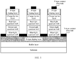
- a GaN-based LED for full-color display when a GaN-based LED for full-color display is prepared, the following method is used: sequentially growing a buffer layer and an N-type doping layer on a substrate, and then growing a sub-pixel structure in each sub-pixel region of the N-type doping layer, where each sub-pixel structure sequentially includes three colors of quantum well structures (that is, a blue-light quantum well structure, a green-light quantum well structure, and a red-light quantum well structure), a charge barrier layer, and a P-type doping layer. Then, an N-type contact electrode and a P-type contact electrode are prepared.
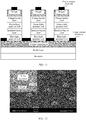
- FIG. 1 A structure of an LED chip prepared by using the foregoing method may be shown in FIG. 1 .
- the LED chip shown in FIG. 1 shows only three sub-pixel structures grown in three sub-pixel regions.
- the three sub-pixel structures are respectively used to emit blue light, green light, and red light.
- the LED chip may include a plurality of sub-pixel structures, each sub-pixel structure may be used as one sub-pixel of the LED chip for full-color display, and every three sub-pixel structures in the plurality of sub-pixel structures may be used as one pixel of the LED chip for full-color display.
- the following describes a principle of implementing full-color display by using the LED chip shown in FIG. 1 .
- a light-emitting wavelength of the quantum well structure is controlled by changing a proportion of indium (In) doped in the quantum well structure, to implement display of three colors: blue, green, and red.
- a proportion of In doped in the blue-light quantum well structure is controlled, so that the blue-light quantum well structure can emit blue light when a light emitting wavelength of the blue-light quantum well structure is 450 nm to 480 nm.
- a proportion of In doped in the green-light quantum well structure is controlled, so that the green-light quantum well structure can emit green light when a light emitting wavelength of the green-light quantum well structure is 500 nm to 550 nm.
- a proportion of In doped in the red-light quantum well structure is controlled, so that the red-light quantum well structure can emit red light when a light-emitting wavelength of the red-light quantum well structure is 620 nm to 700 nm.
- a blue light filter is disposed in a region corresponding to a left-side sub-pixel structure. Because the blue filter can filter out other color light other than blue light, blue light can be emitted in a region above the blue light filter.
- a green light filter is disposed in a region corresponding to a middle sub-pixel structure. Because the green light filter can filter out other color light other than green light, green light can be emitted in a region above the green light filter.
- a red light filter is disposed in a region corresponding to a right-side sub-pixel structure. Because the red light filter can filter out other color light other than red light, red light can be emitted in a region above the red light filter.
- a red-light quantum well structure requires a high doping proportion of In.
- excessively doping In may cause defects and misplacement of the red-light quantum well structure.
- the finally obtained red-light quantum well structure has low light-emitting efficiency and high power consumption.
- the embodiments of this application provide an LED chip and a preparation method therefor, to implement full-color display, improve light-emitting efficiency, and reduce power consumption.
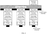
- FIG. 2 is a schematic structural diagram of an LED chip according to an embodiment of this application.
- the LED chip includes the following four parts:
- Each of the three sub-pixel structures includes a blue-light quantum well structure, an interface barrier layer, a green-light quantum well structure, a charge barrier layer, and a P-type GaN doping layer that grow in sequence.
- a colloidal quantum dot is a chemically synthesized inorganic nanomaterial having a quasi-zero-dimensional structure.
- a colloidal quantum dot structure can implement absorption and conversion of spectral energy. When absorbing spectral energy, the colloidal quantum dot structure can absorb spectral energy of various short-wavelength color light.
- a light-emitting wavelength of a colloidal quantum dot may be controlled by controlling a size of the colloidal quantum dot structure, so that the colloidal quantum dot emits different colors of light.
- the red-light colloidal quantum dot structure may absorb blue light emitted by the blue-light quantum well structure, and/or green light emitted by the green-light quantum well structure.
- a size of the red-light colloidal quantum dot structure is controlled, so that a light-emitting wavelength of the red-light colloidal quantum dot structure can be a light-emitting wavelength of red light (for example, can be 620 nm to 700 nm). In this case, the red-light colloidal quantum dot structure can emit red light.
- the red-light colloidal quantum dot structure may include a plurality of colloidal quantum dots.
- Each colloidal quantum dot includes three parts: a core, a shell, and a ligand.
- a material of the core may be CdSe, CdTe, InP, ZnS, GaAs, HgTe, HgSe, InGaP, PbS, PbSe, PbTe, InSe, CuInGaS2, Guln, GaSe2, or the like.
- a material of the shell may be CdS, ZnS, or ZnSe.
- a material of the ligand may be siloxane, oleic acid, or the like.
- the red-light colloidal quantum dot may be further encapsulated by using epoxy resin.
- the red-light colloidal quantum dot structure is used to absorb blue light and/or green light to emit red light. Therefore, a red-light quantum well structure does not need to be disposed in the LED chip. In this way, there is no defect or misplacement of a red-light quantum well structure due to high doping proportion of In in an existing GaN-based LED chip.
- the red-light colloidal quantum dot structure is used to absorb blue light and/or green light to implement red light. In this way, light-emitting efficiency of the LED chip can be improved, thereby reducing power consumption of the LED chip.
- red light may be emitted in a region corresponding to a first sub-pixel structure, by using the disposed red-light colloidal quantum dots.
- the other two sub-pixel structures other than the first sub-pixel structure in the three sub-pixel structures also include the blue-light quantum well structure and the green-light quantum well structure. Therefore, blue light and green light may be respectively displayed by using the other two sub-pixel structures.
- a light filter may be disposed in a corresponding light-emitting region.
- the LED chip shown in FIG. 2 may further include: a red light filter disposed on the red-light colloidal quantum dot structure; a blue light filter disposed in a region that corresponds to a second sub-pixel region in the three sub-pixel regions and that is at the second surface of the N-type GaN doping layer; and a green light filter disposed in a region that corresponds to a third sub-pixel region in the three sub-pixel regions and that is at the second surface of the N-type GaN doping layer.
- the second sub-pixel region may be used to emit blue light
- the third sub-pixel region may be used to emit green light.
- the red light filter disposed on the red-light colloidal quantum dots can be used to filter out color light (for example, blue light and green light) other than red light in the first sub-pixel region.
- the blue light filter disposed in the region corresponding to the second sub-pixel region can be used to filter out color light (for example, green light) other than blue light in the second sub-pixel region.
- the green light filter disposed in the region corresponding to the third sub-pixel region can be used to filter out color light (for example, blue light) other than green light in the third sub-pixel region.
- red light can be emitted in a region above the red light filter
- green light can be emitted in a region above the green light filter
- blue light can be emitted in a region above the blue light filter.
- the charge barrier layer can reduce charge leakage of the sub-pixel structure.
- the charge barrier layer may be made of Al 0.15 Ga 0.85 N, and a thickness of the charge barrier layer may be 15 nm to 35 nm.
- the N-type GaN doping layer may be a GaN layer doped with silicon, and a thickness of the N-type GaN doping layer may be 2 ⁇ m to 3 ⁇ m.
- the P-type GaN doping layer may be a GaN layer doped with magnesium, and a thickness of the P-type GaN doping layer may be 150 nm to 300 nm.
- the first surface of the N-type GaN doping layer may be divided into the three sub-pixel regions and the remaining region other than the three sub-pixel regions.
- the three sub-pixel regions are respectively used to form the three sub-pixel structures, and the three sub-pixel structures are respectively used to emit blue light, green light, and red light, to implement full-color display of the LED chip.
- the three sub-pixel structures may be formed in an etching manner. To be specific, a mask pattern that includes sub-pixel regions and a remaining region through division is prepared, and etching is performed on a structure in the remaining region based on the mask pattern, to form the sub-pixel structures.
- the sub-pixel region is merely obtained after region division to form the sub-pixel structure, and does not represent any actual structure.
- region division at the first surface of the N-type GaN doping layer may be shown in FIG. 4 .
- a light gray region represents a sub-pixel region
- a dark gray region represents a remaining region other than the three sub-pixel regions at the first surface of the N-type GaN doping layer. It is not difficult to imagine that the sub-pixel structure formed in the sub-pixel region shown in FIG. 4 is a cylindrical structure.
- a shape of a pixel may be a circle or a square. Therefore, the three sub-pixel regions in this embodiment of this application may all be circular regions, or may all be square regions.
- a size of the sub-pixel region may be set based on different requirements for the LED chip. This is not specifically limited in this embodiment of this application. For example, a diameter of a circular region may be 5 ⁇ m to 50 ⁇ m.
- the blue-light quantum well structure may include N blue-light quantum well layers, and N+1 isolation layers that are used to isolate the N blue-light quantum well layers and that are alternately formed with the N blue-light quantum well layers, where N ⁇ 1.
- the green-light quantum well structure may include M green-light quantum well layers, and M+1 isolation layers that are used to isolate the M green-light quantum well layers and that are alternately formed with the M green-light quantum well layers, where M ⁇ 1.
- the quantum well structure is formed by alternately growing the isolation layer and the quantum well layer.
- the quantum well structure may be formed through three to five cycles of material growth processes.
- the blue-light quantum well structure may include two blue-light quantum well layers and three isolation layers that are alternately formed with the two blue-light quantum well layers.
- the blue-light quantum well layer may be made of GaN doped with In, which may be specifically represented by In x Ga 1-x N.
- the green-light quantum well layer may be made of GaN doped with In, which may be specifically represented by In x Ga 1-x N.
- a difference is that a doping proportion of In in the blue-light quantum well layer is different from that in the green-light quantum well layer, that is, values of x are different.
- Different doping proportions of In in the quantum well layer indicate different light-emitting wavelengths of the quantum well layer.
- the light-emitting wavelength of the quantum well layer can be controlled by controlling the doping proportion of In in the quantum well layer.
- a light-emitting wavelength of the quantum well layer is 460 nm.
- the quantum well layer can be used to emit blue light, that is, the quantum well layer is the blue-light quantum well layer.
- a light-emitting wavelength of the quantum well layer is 5300 nm.
- the quantum well layer can be used to emit green light, that is, the quantum well layer is the green-light quantum well layer.
- a thickness of the blue-light quantum well layer may be 2 nm to 5 nm, and a thickness of the green-light quantum well layer may also be 2 nm to 5 nm.
- the isolation layer may be made of GaN, and a thickness of the isolation layer may be 7 nm to 15 nm.
- the LED chip shown in FIG. 2 may further include a drive circuit connected to the three P-type contact electrodes and the N-type contact electrode.
- the drive circuit may include a thin film transistor (thin film transistor, TFT), low temperature poly-silicon (low temperature poly-silicon, LTPS), a complementary metal-oxide-semiconductor (complementary metal-oxide-semiconductor, CMOS), and the like.
- the drive circuit may control luminous intensity of each sub-pixel structure by using a pulse-width modulation (pulse-width modulation, PWM) technology, so that blue light, green light, and red light emitted by all the sub-pixel structures in the LED chip have same color brightness.
- PWM pulse-width modulation
- the LED chip when the LED chip is prepared, materials need to be grown on a substrate and a buffer layer. After the material growth is completed, cleavage may be performed on the substrate and the buffer layer because functions of the substrate and the buffer layer have been completed.
- the LED chip obtained after the cleavage may be shown in FIG. 2 , FIG. 3 , and FIG. 5 . In other words, the LED chip does not include the substrate and the buffer layer. In addition, because the substrate and the buffer layer do not affect light-emitting display of the LED chip, cleavage may not be performed on the substrate and the buffer layer.
- the LED chip further includes: a buffer layer and a substrate that are formed at the second surface of the N-type GaN doping layer.
- the buffer layer is adjacent to the N-type GaN doping layer
- the substrate is adjacent to the buffer layer and the red-light colloidal quantum dot structure.
- the substrate may be any one of a sapphire substrate, a Si substrate, a SiC substrate, or a GaN substrate; and the buffer layer may be a GaN buffer layer, where a thickness of the buffer layer may be selected from 2 ⁇ m to 3 ⁇ m.
- the LED chip shown in FIG. 2 includes only three sub-pixel structures.
- the LED chip includes only one pixel.
- the LED chip may include a plurality of sub-pixel structures, and every three of the plurality of sub-pixel structures are a group used as one pixel of the LED chip.
- a structure of each pixel may be shown in FIG. 2 .
- Each pixel is a basic unit for full-color display of the LED chip.
- each of the three sub-pixel structures includes a blue-light quantum well structure and a green-light quantum well structure
- the LED chip may emit blue light and green light by using the other two sub-pixel structures other than the first sub-pixel structure in the three sub-pixel structures.
- the red-light colloidal quantum dot structure may be used for coating in a region corresponding to the first sub-pixel structure. In this way, blue light or green light is absorbed and then converted into red light by using the red-light colloidal quantum dot structure, and the LED chip emits red light. Therefore, full-color display can be implemented by using the LED chip shown in FIG. 2 .
- the red-light colloidal quantum dot structure has characteristics such as narrow line width and high photoluminescence fluorescence efficiency
- the red-light colloidal quantum dot structure is used to absorb blue light and green light, to implement a solution in which the LED chip for full-color display emits red light.
- the solution is compared with a solution in the prior art in which the LED chip emits red light by using a red-light quantum well structure, the light-emitting efficiency of the LED chip can be improved, thereby reducing power consumption of the LED chip.
- this embodiment of this application further provides another LED chip.
- the LED chip includes the following four parts:
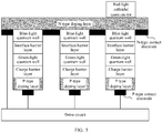
- a first sub-pixel structure in a first sub-pixel region of the three sub-pixel regions includes a blue-light quantum well structure or a green-light quantum well structure, a charge barrier layer, and a P-type GaN doping layer that grow in sequence.
- a second sub-pixel structure in a second sub-pixel region of the three sub-pixel regions includes a blue-light quantum well structure, a charge barrier layer, and a P-type GaN doping layer that grow in sequence.
- a third sub-pixel structure in a third sub-pixel region of the three sub-pixel regions includes a green-light quantum well structure, a charge barrier layer, and a P-type GaN doping layer that grow in sequence.
- red-light colloidal quantum dot structure For a structure, a material, a light-emitting principle, a light-emitting effect, a size setting, and the like of the red-light colloidal quantum dot structure, refer to the related descriptions of the LED chip shown in FIG. 2 . Details are not described herein again.
- the first sub-pixel structure includes either of the blue-light quantum well structure and the green-light quantum well structure.
- the red-light colloidal quantum dot structure may emit red light by absorbing spectral energy of blue light, or may emit red light by absorbing spectral energy of green light.
- conversion efficiency obtained after the red-light colloidal quantum dot structure absorbs the spectral energy of blue light is relatively high. Therefore, when the first sub-pixel structure of the LED chip shown in FIG. 7 includes the blue-light quantum well structure, the LED chip has higher light-emitting efficiency.
- red light may be emitted in a region corresponding to the first sub-pixel structure, by using the disposed red-light colloidal quantum dot structure.
- the second sub-pixel structure in the three sub-pixel structures includes the blue-light quantum well structure
- display of blue light can be implemented by using the second sub-pixel structure
- the third sub-pixel structure in the three sub-pixel structures includes the green-light quantum well structure
- display of green light can be implemented by using the third sub-pixel structure.
- a light filter may be disposed in a corresponding light-emitting region.
- the LED chip shown in FIG. 7 may further include: a red light filter disposed on the red-light colloidal quantum dot structure; a blue light filter disposed in a region that corresponds to the second sub-pixel region and that is at the second surface of the N-type GaN doping layer; and a green light filter disposed in a region that corresponds to the third sub-pixel region and that is at the second surface of the N-type GaN doping layer.
- the red light filter disposed on the red-light colloidal quantum dots can be used to filter out color light (for example, blue light or green light) other than red light in the first sub-pixel region.
- the blue light filter disposed in the region corresponding to the second sub-pixel region can be used to filter out color light (for example, green light) other than blue light in the second sub-pixel region.
- the green light filter disposed in the region corresponding to the third sub-pixel region can be used to filter out color light (for example, blue light) other than green light in the third sub-pixel region.
- red light can be emitted in a region above the red light filter
- green light can be emitted in a region above the green light filter
- blue light can be emitted in a region above the blue light filter.
- the charge barrier layer can reduce charge leakage of the sub-pixel structure.
- the charge barrier layer may be made of Al 0.15 Ga 0.85 N, and a thickness of the charge barrier layer may be 15 nm to 35 nm.
- the N-type GaN doping layer may be a GaN layer doped with silicon, and a thickness of the N-type GaN doping layer may be 2 ⁇ m to 3 ⁇ m.
- the P-type GaN doping layer in the first sub-pixel structure, the P-type GaN doping layer in the second sub-pixel structure, and the P-type GaN doping layer in the third sub-pixel structure each may be a GaN layer doped with magnesium, and a thickness of the P-type GaN doping layer may be 150 nm to 300 nm.
- the blue-light quantum well structure in the second sub-pixel structure may include N blue-light quantum well layers, and N+1 isolation layers that are used to isolate the N blue-light quantum well layers and that are alternately formed with the N blue-light quantum well layers, where N ⁇ 1.
- the green-light quantum well structure in the third sub-pixel structure may include M green-light quantum well layers, and M+1 isolation layers that are used to isolate the M green-light quantum well layers and that are alternately formed with the M green-light quantum well layers, where M ⁇ 1.
- a structure of the blue-light quantum well structure in the first sub-pixel structure may be the same as that of the blue-light quantum well structure in the second sub-pixel structure. If the first sub-pixel structure includes the green-light quantum well structure, a structure of the green-light quantum well structure in the first sub-pixel structure may be the same as that of the green-light quantum well structure in the third sub-pixel structure.
- the LED chip shown in FIG. 7 may further include a drive circuit connected to the three P-type contact electrodes and the N-type contact electrode.
- the drive circuit may control luminous intensity of each sub-pixel structure by using a PWM technology, so that blue light, green light, and red light emitted by all the sub-pixel structures in the LED chip have same color brightness.
- the LED chip shown in FIG. 7 when the LED chip shown in FIG. 7 is prepared, if cleavage is not performed on the substrate and the buffer layer after the material growth is completed, the LED chip further includes: a buffer layer and a substrate that are formed at the second surface of the N-type GaN doping layer, where the buffer layer is adjacent to the N-type GaN doping layer, and the substrate is adjacent to the buffer layer and the red-light colloidal quantum dot structure.
- the LED chip shown in FIG. 7 includes only three sub-pixel structures. In other words, the LED chip includes only one pixel. In actual implementation, the LED chip may include a plurality of sub-pixel structures, and every three of the plurality of sub-pixel structures are a group used as one pixel of the LED chip. A structure of each pixel may be shown in FIG. 7 . Each pixel is a basic unit for full-color display of the LED chip.
- the LED chip shown in FIG. 7 because the second sub-pixel structure in the three sub-pixel structures includes the blue-light quantum well structure, the LED chip can emit blue light by using the second sub-pixel structure; and because the third sub-pixel structure in the three sub-pixel structures includes the green-light quantum well structure, the LED chip can emit green light by using the third sub-pixel structure.
- a red-light colloidal quantum dot structure may be used for coating in a region corresponding to the first sub-pixel structure that includes the blue-light quantum well structure or the green-light quantum well structure. In this way, blue light or green light is absorbed and then converted into red light by using the red-light colloidal quantum dot structure, and the LED chip emits red light. Therefore, full-color display can be implemented by using the LED chip provided in the foregoing solution.
- the red-light colloidal quantum dot structure has characteristics such as narrow line width and high photoluminescence fluorescence efficiency
- the red-light colloidal quantum dot structure is used to absorb blue light and green light, to implement a solution in which the LED chip for full-color display emits red light.
- the solution is compared with a solution in the prior art in which the LED chip emits red light by using a red-light quantum well structure, the light-emitting efficiency of the LED chip can be improved, thereby reducing power consumption of the LED chip.
- each sub-pixel structure includes a blue-light quantum well structure and a green-light quantum well structure.
- the red light can be emitted after the first sub-pixel structure on which the red-light colloidal quantum dots are correspondingly disposed absorbs blue light and green light.
- which sub-pixel structure emits blue light and which sub-pixel structure emits green light depend on a color of a disposed light filter.
- a sub-pixel structure on which the blue light filter is correspondingly disposed is used to emit blue light
- a sub-pixel structure on which the green light filter is correspondingly disposed is used to emit green light.
- the internal structures of all the sub-pixel structures are different.
- the first sub-pixel structure includes one of the blue-light quantum well structure or the green-light quantum well structure
- the second sub-pixel structure includes the blue-light quantum well structure
- the third sub-pixel structure includes the green-light quantum well structure.
- the red light can be emitted after the first sub-pixel structure on which the red-light colloidal quantum dots are correspondingly disposed absorbs blue light or green light.
- the second sub-pixel structure including the blue-light quantum well structure is used to emit blue light
- the third sub-pixel structure including the green-light quantum well structure is used to emit green light.
- the LED chip shown in FIG. 2 or the LED chip shown in FIG. 7 may be selectively used.
- the LED chip shown in FIG. 2 When the LED chip shown in FIG. 2 is prepared, because the structures of all the sub-pixel structures are the same, in a material growth process of the LED chip, it is unnecessary to consider which sub-pixel structure is used to emit which color of light. In other words, it is unnecessary to separately perform material growth for different sub-pixel structures, an operation procedure for the material growth process can be simplified. Therefore, if it is expected to simplify a preparation procedure of the LED chip, the LED chip shown in FIG. 2 may be used.
- the LED chip shown in FIG. 7 When the LED chip shown in FIG. 7 is prepared, some parts of materials need to be grown first during material growth. After a mask is used to protect the grown materials, other parts of materials are grown. Although a procedure of the material growth process is relatively complex, a structure of the LED chip (that is, the LED chip shown in FIG. 7 ) prepared in this manner is simpler than a structure of the LED chip shown in FIG. 2 . This manner is applicable to a scenario in which there is a relatively high requirement for simplifying a structure of an LED chip.
- the LED chip shown in FIG. 2 and the LED chip shown in FIG. 7 are two typical LED chips provided in the embodiments of this application. Based on two embodiments, the following describes preparation methods of the two typical LED chips provided in the embodiments of this application.
- This embodiment of this application provides a preparation method for an LED chip.
- the method is used to prepare the LED chip shown in FIG. 2 .
- the method includes the following steps: S1001: Sequentially grow a buffer layer, an N-type GaN doping layer, a blue-light quantum well structure, an interface barrier layer, a green-light quantum well structure, a charge barrier layer, and a P-type GaN doping layer at a first surface of a substrate, to form a first sample.
- step S1001 material growth may be performed in a metal organic chemical vapor deposition (metalorganic chemical vapor deposition, MOCVD) manner.
- MOCVD metal organic chemical vapor deposition
- the substrate may be any one of a sapphire substrate, a Si substrate, a SiC substrate, or a GaN substrate.
- the buffer layer may be a GaN buffer layer, and a thickness of the buffer layer may be selected from 2 ⁇ m to 3 ⁇ m.
- the N-type GaN doping layer may be a GaN layer doped with silicon, and a thickness of the N-type GaN doping layer may be 2 ⁇ m to 3 ⁇ m.
- the P-type GaN doping layer may be a GaN layer doped with magnesium, and a thickness of the P-type GaN doping layer may be 150 nm to 300 nm.
- the charge barrier layer can reduce charge leakage of a sub-pixel structure.
- the charge barrier layer may be made of Al 0.15 Ga 0.85 N, and a thickness of the charge barrier layer may be 15 nm to 35 nm.
- S1002 Transfer a mask pattern to the P-type GaN doping layer, to form a second sample.
- the mask pattern includes a plurality of sub-pixel regions and a remaining region other than the plurality of sub-pixel regions.
- the first sample grown in step S1001 may be divided to a plurality of sub-pixel regions and a remaining region by using the mask pattern.
- S1003 Perform etching on the second sample based on the mask pattern, protect structures in the plurality of sub-pixel regions, and expose the N-type GaN doping layer in the remaining region, to form a third sample.
- step S1003 the performing etching on the second sample based on the mask pattern, protecting structures in the plurality of sub-pixel regions, and exposing the N-type GaN doping layer in the remaining region other than the plurality of sub-pixel regions in the mask pattern may be implemented in the following manner: passivating and protecting a side surface of the LED chip and the plurality of sub-pixel regions; and performing etching on the remaining region by using inductively coupled plasma (inductive coupled plasma, ICP) or through reactive ion etching (reactive ion etching, RIE), so that the N-type GaN doping layer in the remaining region is exposed.
- ICP inductive coupled plasma
- RIE reactive ion etching
- S1004 Respectively form a plurality of P-type contact electrodes in the plurality of sub-pixel regions in the third sample, and form an N-type contact electrode in the remaining region, to form a fourth sample.
- step S1004 the respectively forming a plurality of P-type contact electrodes in the plurality of sub-pixel regions, and forming an N-type contact electrode in the remaining region may be implemented in the following manner: evaporating and depositing a gold-nickel alloy by using an electron beam, and respectively forming the plurality of P-type contact electrodes in the plurality of sub-pixel regions after annealing at 200°C to 500°C; and sputtering indium tin oxide (ITO) or graphite in the remaining region, to form the N-type contact electrode.
- the plurality of sub-pixel structures share one N-type contact electrode.
- the N-type contact electrode may also be referred to as a common cathode.
- FIG. 11 shows an LED chip including only three sub-pixel structures.
- the fourth sample obtained after step S1004 is performed may include a plurality of sub-pixel structures, and every three sub-pixel structures in the plurality of sub-pixel structures may be used as one pixel to implement full-color display.
- each protruding cylindrical structure represents one sub-pixel structure, and each sub-pixel structure includes a p-contact (that is, a P-type contact electrode).
- a planar region other than the protruding parts may be considered as the remaining region other than the sub-pixel regions, and an N-type contact electrode is formed in the region.
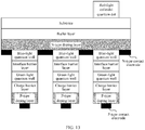
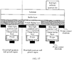
- S1005 Use at least one red-light colloidal quantum dot structure for coating in a region that is at a second surface of the substrate and that corresponds to at least one first sub-pixel region in the plurality of sub-pixel regions that is used to emit red light, to form an LED chip.
- the LED chip prepared by using the method shown in FIG. 10 may be shown in FIG. 13 . It should be noted that the LED chip shown in FIG. 13 includes only three sub-pixel structures. In actual implementation, the LED chip prepared by using the method shown in FIG. 10 may include a plurality of sub-pixel structures, every three sub-pixel structures may form one pixel, and each pixel is used as a basic unit for full-color display of the LED chip.
- the method shown in FIG. 10 may further include: respectively disposing at least one red light filter on the at least one red-light colloidal quantum dot structure; respectively disposing at least one blue light filter in a region that is at the second surface of the substrate and that corresponds to at least one second sub-pixel region in the plurality of sub-pixel regions that is used to emit blue light; and respectively disposing at least one green light filter in a region that is at the second surface of the substrate and that corresponds to at least one third sub-pixel region in the plurality of sub-pixel regions that is used to emit green light.
- Different colors of light filters are disposed at the second surface of the substrate, so that other color light other than the color of light can be filtered out, thereby improving color purity of the LED chip used for full-color display.
- the method shown in FIG. 10 may further include: connecting a drive circuit to the plurality of P-type contact electrodes and the N-type contact electrode through alignment by using a metal solder ball.
- APWM current of the drive circuit may be controlled to control luminous intensity of each sub-pixel structure, so that blue light, green light, and red light emitted by all the sub-pixel structures in the LED chip have same color brightness.
- cleavage may be further performed between the LED chip and each of the substrate and the buffer layer in a laser radiation manner.
- an operation of using the at least one red-light colloidal quantum dot structure for coating may be implemented in the following manner: respectively using the at least one red-light colloidal quantum dot structure for coating in the region that is at the surface of the N-type GaN doping layer adjacent to the buffer layer and that corresponds to the at least one first sub-pixel region.
- cleavage may be performed on the substrate and the buffer layer because functions of the substrate and the buffer layer have been completed, so that a structure of the LED chip is simplified.
- FIG. 14 a possible structure of the LED chip prepared in the manner shown in FIG. 10 may be shown in FIG. 14 .
- the LED chip shown in FIG. 14 may be considered as a specific example of the LED chip shown in FIG. 2 .
- the method shown in FIG. 10 may be used to prepare the LED chip shown in FIG. 2 .
- the method shown in FIG. 10 may be used to prepare the LED chip shown in FIG. 2 .
- the method shown in FIG. 10 may be used to prepare the LED chip shown in FIG. 2 .
- This embodiment of this application provides a preparation method for an LED chip.
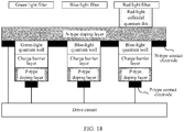
- the method may be used to prepare the LED chip shown in FIG. 7 .
- the method includes the following steps: S1501: Sequentially grow a buffer layer and an N-type GaN doping layer at a first surface of a substrate.
- the substrate may be any one of a sapphire substrate, a Si substrate, a SiC substrate, or a GaN substrate.
- the buffer layer may be a GaN buffer layer, and a thickness of the buffer layer may be selected from 2 ⁇ m to 3 ⁇ m.
- the N-type GaN doping layer may be a GaN layer doped with silicon, and a thickness of the N-type GaN doping layer may be 2 ⁇ m to 3 ⁇ m.
- S1502 Sequentially grow a blue-light quantum well structure, a charge barrier layer, and a P-type GaN doping layer in a blue-light quantum well growth region at the N-type GaN doping layer, and sequentially grow a green-light quantum well structure, a charge barrier layer, and a P-type GaN doping layer in a green-light quantum well growth region other than the blue-light quantum well growth region at the N-type GaN doping layer, to form a first sample.
- step S1502 in material growth, the N-type GaN doping layer is divided to the blue-light quantum well growth region and the green-light quantum well growth region, and different structures are grown in different quantum well growth regions.
- the material growth process in step S1502 may be implemented in the following manner: preparing a first mask at the N-type GaN doping layer, where the first mask is used to protect the green-light quantum well growth region; sequentially growing the blue-light quantum well structure, the charge barrier layer, and the P-type GaN doping layer in the blue-light quantum well growth region; removing the first mask; preparing a second mask in the blue-light quantum well growth region, where the second mask is used to protect the blue-light quantum well growth region; and sequentially growing the green-light quantum well structure, the charge barrier layer, and the P-type GaN doping layer in the green-light quantum well growth region.
- S1503 Transfer a mask pattern to the P-type GaN doping layer, to form a second sample.
- the mask pattern includes a plurality of sub-pixel regions and a remaining region other than the plurality of sub-pixel regions.
- the plurality of sub-pixel regions include at least one first sub-pixel region used to emit red light, at least one second sub-pixel region used to emit blue light, and at least one third sub-pixel region used to emit green light.
- the at least one first sub-pixel region is aligned with the blue-light quantum well growth region or the green-light quantum well growth region.
- the at least one second sub-pixel region is aligned with the blue-light quantum well growth region.
- At least one third sub-pixel region is aligned with the green-light quantum well growth region.
- the first sample grown in step S1502 may be divided to a plurality of sub-pixel regions and a remaining region by using the mask pattern.
- S1504 Perform etching on the second sample based on the mask pattern, protect structures in the plurality of sub-pixel regions, and expose the N-type GaN doping layer in the remaining region, to form a third sample.
- corresponding structures in the at least one second sub-pixel region obtained after the etching are structures grown in the blue-light quantum well growth region, that is, the blue-light quantum well structure, the charge barrier layer, and the P-type GaN doping layer.
- the LED chip can emit blue light by using the structure.
- the at least one third sub-pixel region in the mask pattern is aligned with the green-light quantum well growth region, corresponding structures in the at least one third sub-pixel region obtained after the etching are structures grown in the green-light quantum well growth region, that is, the green-light quantum well structure, the charge barrier layer, and the P-type GaN doping layer.
- the LED chip can emit green light by using the structure.
- the at least one first sub-pixel region is aligned with the blue-light quantum well growth region or the green-light quantum well growth region. Therefore, after the etching, the LED chip can emit red light by using red-light colloidal quantum dots for coating in a corresponding structure in the first sub-pixel region.
- step S1504 the performing etching on the second sample based on the mask pattern, protecting structures in the plurality of sub-pixel regions, and exposing the N-type GaN doping layer in the remaining region other than the plurality of sub-pixel regions in the mask pattern may be implemented in the following manner: passivating and protecting a side surface of the LED chip and the plurality of sub-pixel regions; and performing etching on the remaining region in an ICP manner or an RIE manner, so that the N-type GaN doping layer in the remaining region is exposed.
- S1505 Respectively form a plurality of P-type contact electrodes in the plurality of sub-pixel regions in the third sample, and form an N-type contact electrode in the remaining region, to form a fourth sample.
- step S1505 the respectively forming a plurality of P-type contact electrodes in the plurality of sub-pixel regions, and forming an N-type contact electrode in the remaining region may be implemented in the following manner: evaporating and depositing a gold-nickel alloy by using an electron beam, and respectively forming the plurality of P-type contact electrodes in the plurality of sub-pixel regions after annealing at 200°C to 500°C; and sputtering indium tin oxide (ITO) or graphite in the remaining region, to form the N-type contact electrode.
- the plurality of sub-pixel structures share one N-type contact electrode.
- the N-type contact electrode may also be referred to as a common cathode.
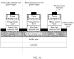
- a structure of the formed fourth sample may be shown in FIG. 16 .
- FIG. 16 shows an LED chip including only three sub-pixel structures.
- the fourth sample obtained after step S1505 is performed may include a plurality of sub-pixel structures, and every three sub-pixel structures in the plurality of sub-pixel structures may be used as one pixel to implement full-color display.
- the at least one first sub-pixel region is aligned with the blue-light quantum well growth region.
- S1506 Respectively use at least one red-light colloidal quantum dot structure for coating in a region that is at a second surface of the substrate and that corresponds to the at least one first sub-pixel region, to form an LED chip.
- Step S 1506 is performed on the fourth sample shown in FIG. 16 , to obtain the LED chip shown in FIG. 17 .
- the LED chip shown in FIG. 17 includes only three sub-pixel structures.
- the LED chip prepared by using the method shown in FIG. 15 may include a plurality of sub-pixel structures, every three sub-pixel structures may form one pixel, and each pixel is used as a basic unit for full-color display of the LED chip.
- the method shown in FIG. 15 may further include: respectively disposing at least one red light filter on the at least one red-light colloidal quantum dot structure; respectively disposing at least one blue light filter in a region that is at the second surface of the substrate and that corresponds to the at least one second sub-pixel region; and respectively disposing at least one green light filter in a region that is at the second surface of the substrate and that corresponds to the at least one third sub-pixel region.
- Different colors of light filters are disposed at the second surface of the substrate, so that other color light other than the color of light can be filtered out, thereby improving color purity of the LED chip used for full-color display.
- the method shown in FIG. 15 may further include: connecting a drive circuit to the plurality of P-type contact electrodes and the N-type contact electrode through alignment by using a metal solder ball.
- APWM current of the drive circuit may be controlled to control luminous intensity of each sub-pixel structure, so that blue light, green light, and red light emitted by all the sub-pixel structures in the LED chip have same color brightness.
- cleavage may be further performed between the LED chip and each of the substrate and the buffer layer in a laser radiation manner.
- an operation of using the at least one red-light colloidal quantum dot structure for coating may be implemented in the following manner: respectively using the at least one red-light colloidal quantum dot structure for coating in the region that is at the surface of the N-type GaN doping layer adjacent to the buffer layer and that corresponds to the at least one first sub-pixel region.
- cleavage may be performed on the substrate and the buffer layer because functions of the substrate and the buffer layer have been completed, so that a structure of the LED chip is simplified.
- FIG. 18 a possible structure of the LED chip prepared in the manner shown in FIG. 15 may be shown in FIG. 18 .
- the LED chip shown in FIG. 18 may be considered as a specific example of the LED chip shown in FIG. 7 .
- Embodiment 2 and Embodiment 1 are different only in a material growth process (that is, S1001 in FIG. 10 , and S1501 and S1502 in FIG. 15 ), and other preparation steps are similar or the same. However, due to different material growth steps, structures of LED chips finally obtained after the preparation are different.
- the method shown in FIG. 15 may be used to prepare the LED chip shown in FIG. 7 .
- the method shown in FIG. 15 may be used to prepare the LED chip shown in FIG. 7 .
- the method shown in FIG. 15 may be used to prepare the LED chip shown in FIG. 7 .
- the related descriptions of the LED chip shown in FIG. 7 refer to the related descriptions of the LED chip shown in FIG. 7 .
- the embodiments of this application provide the LED chip and the preparation method therefor.
- full-color display can be implemented by using the LED chip.
Landscapes
- Led Devices (AREA)
- Led Device Packages (AREA)
Applications Claiming Priority (2)
| Application Number | Priority Date | Filing Date | Title |
|---|---|---|---|
| CN201810168757.XA CN110212064B (zh) | 2018-02-28 | 2018-02-28 | 一种发光二极管芯片及其制备方法 |
| PCT/CN2018/098389 WO2019165755A1 (zh) | 2018-02-28 | 2018-08-02 | 一种发光二极管芯片及其制备方法 |
Publications (3)
| Publication Number | Publication Date |
|---|---|
| EP3748700A1 true EP3748700A1 (de) | 2020-12-09 |
| EP3748700A4 EP3748700A4 (de) | 2021-04-14 |
| EP3748700B1 EP3748700B1 (de) | 2025-10-08 |
Family
ID=67778763
Family Applications (1)
| Application Number | Title | Priority Date | Filing Date |
|---|---|---|---|
| EP18908112.8A Active EP3748700B1 (de) | 2018-02-28 | 2018-08-02 | Leuchtdiodenchip und herstellungsverfahren dafür |
Country Status (4)
| Country | Link |
|---|---|
| US (1) | US11296257B2 (de) |
| EP (1) | EP3748700B1 (de) |
| CN (1) | CN110212064B (de) |
| WO (1) | WO2019165755A1 (de) |
Families Citing this family (14)
| Publication number | Priority date | Publication date | Assignee | Title |
|---|---|---|---|---|
| CN110880522B (zh) * | 2019-10-14 | 2022-03-29 | 厦门大学 | 基于极性面和非极性面生长的微型led集成全色显示芯片及其制备方法 |
| CN111326621B (zh) * | 2020-04-03 | 2025-05-27 | 深圳雷曼光电科技股份有限公司 | 一种倒装Micro LED全彩量子点芯片、其制备方法和用途 |
| US11264535B1 (en) * | 2020-08-12 | 2022-03-01 | Jyh-Chia Chen | Pixel device and display using a monolithic blue/green LED combined with red luminescence materials |
| CN112420885A (zh) * | 2020-12-08 | 2021-02-26 | 福建兆元光电有限公司 | 一种集成式Micro LED芯片及其制造方法 |
| CN115708227A (zh) * | 2021-08-18 | 2023-02-21 | 重庆康佳光电技术研究院有限公司 | 一种led芯片及其制备方法、显示面板 |
| CN117374056A (zh) * | 2022-06-30 | 2024-01-09 | 深超光电(深圳)有限公司 | 显示面板及显示面板制造方法 |
| CN115148756B (zh) * | 2022-07-19 | 2025-07-04 | 江西兆驰半导体有限公司 | 一种发光二极管模块及其制备方法 |
| WO2024107372A1 (en) * | 2022-11-18 | 2024-05-23 | Lumileds Llc | Visualization system including direct and converted polychromatic led array |
| CN116111030B (zh) * | 2023-03-20 | 2026-01-23 | 厦门乾照光电股份有限公司 | 一种Micro-LED显示装置及其制作方法 |
| CN116482931B (zh) * | 2023-06-25 | 2023-11-21 | 江西兆驰半导体有限公司 | 用于巨量转移的掩模版及其设计方法、巨量转移方法 |
| CN119993963A (zh) * | 2023-11-08 | 2025-05-13 | 纳微朗科技(深圳)有限公司 | 发光二极管芯片及其芯片组、显示模组 |
| CN117637944B (zh) * | 2024-01-25 | 2024-04-02 | 江西兆驰半导体有限公司 | 一种发光二极管外延片及其制备方法、led芯片 |
| CN120076506A (zh) * | 2024-03-20 | 2025-05-30 | 纳微朗科技(深圳)有限公司 | 发光二极管芯片及其芯片组、显示模组 |
| CN120076505A (zh) * | 2024-03-20 | 2025-05-30 | 纳微朗科技(深圳)有限公司 | 发光二极管芯片及其芯片组、显示模组 |
Family Cites Families (23)
| Publication number | Priority date | Publication date | Assignee | Title |
|---|---|---|---|---|
| US5952681A (en) | 1997-11-24 | 1999-09-14 | Chen; Hsing | Light emitting diode emitting red, green and blue light |
| US7323721B2 (en) * | 2004-09-09 | 2008-01-29 | Blue Photonics Inc. | Monolithic multi-color, multi-quantum well semiconductor LED |
| TWI344314B (en) * | 2005-10-14 | 2011-06-21 | Hon Hai Prec Ind Co Ltd | Light-emitting element, plane light source and direct-type backlight module |
| TWI397192B (zh) * | 2007-08-03 | 2013-05-21 | 友達光電股份有限公司 | 白色發光二極體 |
| CN101800273B (zh) * | 2009-02-11 | 2011-06-01 | 立景光电股份有限公司 | 形成横向分布发光二极管的方法 |
| TW201106505A (en) * | 2009-04-20 | 2011-02-16 | 3M Innovative Properties Co | Non-radiatively pumped wavelength converter |
| CN101771028B (zh) * | 2009-12-25 | 2012-09-05 | 中国科学院上海微系统与信息技术研究所 | 一种白光led芯片及其制造方法 |
| CN102231422A (zh) * | 2011-06-16 | 2011-11-02 | 清华大学 | 一种无荧光粉单芯片GaN基发光二极管及其制备方法 |
| US9159700B2 (en) | 2012-12-10 | 2015-10-13 | LuxVue Technology Corporation | Active matrix emissive micro LED display |
| FR3019380B1 (fr) * | 2014-04-01 | 2017-09-01 | Centre Nat Rech Scient | Pixel semiconducteur, matrice de tels pixels, structure semiconductrice pour la realisation de tels pixels et leurs procedes de fabrication |
| GB201420452D0 (en) | 2014-11-18 | 2014-12-31 | Mled Ltd | Integrated colour led micro-display |
| US9557954B2 (en) | 2014-12-23 | 2017-01-31 | X Development Llc | Display panel using direct emission pixel arrays |
| CN104617121A (zh) * | 2015-01-04 | 2015-05-13 | 中国电子科技集团公司第五十五研究所 | 一种提高有源矩阵微型led显示器光学性能的方法 |
| KR102377794B1 (ko) * | 2015-07-06 | 2022-03-23 | 엘지전자 주식회사 | 반도체 발광 소자를 이용한 디스플레이 장치 및 이의 제조방법 |
| KR102373200B1 (ko) * | 2015-07-14 | 2022-03-17 | 삼성전자주식회사 | 디스플레이 패널 및 상기 디스플레이 패널을 이용하는 디스플레이 장치 |
| US11239394B2 (en) * | 2016-03-18 | 2022-02-01 | Lg Innotek Co., Ltd. | Semiconductor device and display device including the same |
| CN105679196A (zh) * | 2016-04-11 | 2016-06-15 | 深圳市丽格特光电有限公司 | 一种基于氮化镓led和量子点技术的全彩色高分辨率微显示芯片 |
| US9941330B2 (en) * | 2016-05-18 | 2018-04-10 | Globalfoundries Inc. | LEDs with three color RGB pixels for displays |
| CN105977350B (zh) * | 2016-05-23 | 2019-01-08 | 吉林大学 | 基于能量转移机制的量子点发光二极管的制备方法 |
| CN106356463B (zh) * | 2016-10-11 | 2017-12-29 | 深圳市华星光电技术有限公司 | Qled显示装置的制作方法 |
| CN106920790A (zh) | 2017-01-24 | 2017-07-04 | 中山大学 | 一种全彩微显示器件及其制备方法 |
| CN107203064A (zh) * | 2017-07-03 | 2017-09-26 | 厦门天马微电子有限公司 | 一种显示装置 |
| WO2019027820A1 (en) * | 2017-07-31 | 2019-02-07 | Yale University | MICRO-LED NANOPOROUS DEVICES AND METHODS OF MAKING SAME |
-
2018
- 2018-02-28 CN CN201810168757.XA patent/CN110212064B/zh active Active
- 2018-08-02 EP EP18908112.8A patent/EP3748700B1/de active Active
- 2018-08-02 WO PCT/CN2018/098389 patent/WO2019165755A1/zh not_active Ceased
-
2020
- 2020-08-27 US US17/004,958 patent/US11296257B2/en active Active
Also Published As
| Publication number | Publication date |
|---|---|
| CN110212064B (zh) | 2020-10-09 |
| WO2019165755A8 (zh) | 2020-09-17 |
| EP3748700A4 (de) | 2021-04-14 |
| US20200395507A1 (en) | 2020-12-17 |
| WO2019165755A1 (zh) | 2019-09-06 |
| EP3748700B1 (de) | 2025-10-08 |
| CN110212064A (zh) | 2019-09-06 |
| US11296257B2 (en) | 2022-04-05 |
Similar Documents
| Publication | Publication Date | Title |
|---|---|---|
| US11296257B2 (en) | Light-emitting diode chip and preparation method therefor | |
| TWI255569B (en) | White-light emitting device and method for manufacturing the same | |
| JP2019516251A (ja) | 異なる色のledを含むモノリシックマルチカラー直視型ディスプレイおよびそれを製造する方法 | |
| Li et al. | Monolithic full‐color microdisplay using patterned quantum dot photoresist on dual‐wavelength LED epilayers | |
| CN110265586A (zh) | 显示面板及其制造方法 | |
| CN108389941A (zh) | 显指可调的无荧光粉单芯片白光led器件及其制备方法 | |
| US20250275326A1 (en) | Fabrication method for crosstalk-proof structure of integrated colored micro led | |
| CN110265587A (zh) | 显示面板及其制造方法 | |
| CN109148652A (zh) | 无机发光二极管显示面板及其制作方法和显示装置 | |
| CN110311053A (zh) | 显示面板及其制造方法 | |
| CN113690270A (zh) | 用于单芯片micro-LED全彩显示的多量子阱外延生长方法 | |
| CN111146316B (zh) | 一种rgb led集成显示阵列的制备方法 | |
| Xu et al. | Optimized InGaN/GaN quantum structure for high-efficiency micro-LEDs displays with low current injection | |
| US20230261031A1 (en) | Semiconductor light-emitting device and preparation method thereof | |
| JP2002185044A (ja) | 窒化物半導体多色発光素子 | |
| CN209929349U (zh) | 显示面板 | |
| US20120097920A1 (en) | Iii-nitride light-emitting diode and method of producing the same | |
| CN113206176B (zh) | 选区刻蚀外延Micro-LED芯片及其设计、制备方法 | |
| CN209929308U (zh) | 显示面板 | |
| Saito et al. | Characteristics of Stacked GaInN‐Based Red, Green, and Blue Full‐Color Monolithic μLED Arrays Connected via Tunnel Junctions | |
| CN114846629A (zh) | 发光二极管前体及其制备方法 | |
| US12087888B2 (en) | Optoelectronic component with a luminescence conversion layer | |
| US12224269B2 (en) | Optoelectronic device in which the pixels contain light-emitting diodes that emit several colors and manufacturing method | |
| CN109841712A (zh) | 基于类金字塔型的显指可调的单芯片白光led及其制备方法 | |
| CN114005911B (zh) | 一种显示器件及其制备方法 |
Legal Events
| Date | Code | Title | Description |
|---|---|---|---|
| STAA | Information on the status of an ep patent application or granted ep patent |
Free format text: STATUS: THE INTERNATIONAL PUBLICATION HAS BEEN MADE |
|
| PUAI | Public reference made under article 153(3) epc to a published international application that has entered the european phase |
Free format text: ORIGINAL CODE: 0009012 |
|
| STAA | Information on the status of an ep patent application or granted ep patent |
Free format text: STATUS: REQUEST FOR EXAMINATION WAS MADE |
|
| 17P | Request for examination filed |
Effective date: 20200904 |
|
| AK | Designated contracting states |
Kind code of ref document: A1 Designated state(s): AL AT BE BG CH CY CZ DE DK EE ES FI FR GB GR HR HU IE IS IT LI LT LU LV MC MK MT NL NO PL PT RO RS SE SI SK SM TR |
|
| AX | Request for extension of the european patent |
Extension state: BA ME |
|
| A4 | Supplementary search report drawn up and despatched |
Effective date: 20210312 |
|
| RIC1 | Information provided on ipc code assigned before grant |
Ipc: H01L 27/15 20060101AFI20210305BHEP Ipc: H01L 33/50 20100101ALN20210305BHEP Ipc: H01L 33/00 20100101ALN20210305BHEP Ipc: H01L 33/32 20100101ALN20210305BHEP Ipc: H01L 33/38 20100101ALN20210305BHEP Ipc: H01L 33/06 20100101ALN20210305BHEP Ipc: H01L 33/08 20100101ALN20210305BHEP Ipc: H01L 25/075 20060101ALN20210305BHEP |
|
| DAV | Request for validation of the european patent (deleted) | ||
| DAX | Request for extension of the european patent (deleted) | ||
| STAA | Information on the status of an ep patent application or granted ep patent |
Free format text: STATUS: EXAMINATION IS IN PROGRESS |
|
| RIC1 | Information provided on ipc code assigned before grant |
Ipc: H01L 25/075 20060101ALN20220119BHEP Ipc: H01L 33/08 20100101ALN20220119BHEP Ipc: H01L 33/06 20100101ALN20220119BHEP Ipc: H01L 33/38 20100101ALN20220119BHEP Ipc: H01L 33/32 20100101ALN20220119BHEP Ipc: H01L 33/00 20100101ALN20220119BHEP Ipc: H01L 33/50 20100101ALN20220119BHEP Ipc: H01L 27/15 20060101AFI20220119BHEP |
|
| 17Q | First examination report despatched |
Effective date: 20220126 |
|
| REG | Reference to a national code |
Ref country code: DE Free format text: PREVIOUS MAIN CLASS: H01L0033000000 Ref country code: DE Ref legal event code: R079 Ref document number: 602018086278 Country of ref document: DE Free format text: PREVIOUS MAIN CLASS: H01L0033000000 Ipc: H10H0029140000 |
|
| GRAP | Despatch of communication of intention to grant a patent |
Free format text: ORIGINAL CODE: EPIDOSNIGR1 |
|
| STAA | Information on the status of an ep patent application or granted ep patent |
Free format text: STATUS: GRANT OF PATENT IS INTENDED |
|
| RIC1 | Information provided on ipc code assigned before grant |
Ipc: H10H 20/825 20250101ALN20250424BHEP Ipc: H10H 20/813 20250101ALN20250424BHEP Ipc: H10H 29/49 20250101ALN20250424BHEP Ipc: H10H 29/34 20250101ALN20250424BHEP Ipc: H10H 29/80 20250101ALI20250424BHEP Ipc: H10H 29/851 20250101ALI20250424BHEP Ipc: H10H 29/01 20250101ALI20250424BHEP Ipc: H10H 29/14 20250101AFI20250424BHEP |
|
| INTG | Intention to grant announced |
Effective date: 20250514 |
|
| GRAS | Grant fee paid |
Free format text: ORIGINAL CODE: EPIDOSNIGR3 |
|
| GRAA | (expected) grant |
Free format text: ORIGINAL CODE: 0009210 |
|
| STAA | Information on the status of an ep patent application or granted ep patent |
Free format text: STATUS: THE PATENT HAS BEEN GRANTED |
|
| AK | Designated contracting states |
Kind code of ref document: B1 Designated state(s): AL AT BE BG CH CY CZ DE DK EE ES FI FR GB GR HR HU IE IS IT LI LT LU LV MC MK MT NL NO PL PT RO RS SE SI SK SM TR |
|
| REG | Reference to a national code |
Ref country code: GB Ref legal event code: FG4D Ref country code: CH Ref legal event code: F10 Free format text: ST27 STATUS EVENT CODE: U-0-0-F10-F00 (AS PROVIDED BY THE NATIONAL OFFICE) Effective date: 20251008 |
|
| REG | Reference to a national code |
Ref country code: DE Ref legal event code: R096 Ref document number: 602018086278 Country of ref document: DE |
|
| REG | Reference to a national code |
Ref country code: IE Ref legal event code: FG4D |
|
| REG | Reference to a national code |
Ref country code: NL Ref legal event code: MP Effective date: 20251008 |
|
| REG | Reference to a national code |
Ref country code: AT Ref legal event code: MK05 Ref document number: 1846041 Country of ref document: AT Kind code of ref document: T Effective date: 20251008 |
|
| PG25 | Lapsed in a contracting state [announced via postgrant information from national office to epo] |
Ref country code: NL Free format text: LAPSE BECAUSE OF FAILURE TO SUBMIT A TRANSLATION OF THE DESCRIPTION OR TO PAY THE FEE WITHIN THE PRESCRIBED TIME-LIMIT Effective date: 20251008 |