EP3748852A1 - Circuit d'attaque hybride - Google Patents
Circuit d'attaque hybride Download PDFInfo
- Publication number
- EP3748852A1 EP3748852A1 EP19214202.4A EP19214202A EP3748852A1 EP 3748852 A1 EP3748852 A1 EP 3748852A1 EP 19214202 A EP19214202 A EP 19214202A EP 3748852 A1 EP3748852 A1 EP 3748852A1
- Authority
- EP
- European Patent Office
- Prior art keywords
- coupled
- resistor
- diode
- turn
- photo
- Prior art date
- Legal status (The legal status is an assumption and is not a legal conclusion. Google has not performed a legal analysis and makes no representation as to the accuracy of the status listed.)
- Withdrawn
Links
- 230000000630 rising effect Effects 0.000 claims description 30
- 239000003990 capacitor Substances 0.000 claims description 29
- 239000004065 semiconductor Substances 0.000 claims description 4
- 230000005669 field effect Effects 0.000 claims description 3
- 238000010586 diagram Methods 0.000 description 16
- 230000003071 parasitic effect Effects 0.000 description 4
- 230000000694 effects Effects 0.000 description 3
- JMASRVWKEDWRBT-UHFFFAOYSA-N Gallium nitride Chemical compound [Ga]#N JMASRVWKEDWRBT-UHFFFAOYSA-N 0.000 description 1
- 230000003247 decreasing effect Effects 0.000 description 1
- 238000002955 isolation Methods 0.000 description 1
- 238000000034 method Methods 0.000 description 1
Images





Classifications
-
- H—ELECTRICITY
- H03—ELECTRONIC CIRCUITRY
- H03K—PULSE TECHNIQUE
- H03K17/00—Electronic switching or gating, i.e. not by contact-making and –breaking
- H03K17/12—Modifications for increasing the maximum permissible switched current
- H03K17/122—Modifications for increasing the maximum permissible switched current in field-effect transistor switches
-
- H—ELECTRICITY
- H03—ELECTRONIC CIRCUITRY
- H03K—PULSE TECHNIQUE
- H03K17/00—Electronic switching or gating, i.e. not by contact-making and –breaking
- H03K17/51—Electronic switching or gating, i.e. not by contact-making and –breaking characterised by the components used
- H03K17/56—Electronic switching or gating, i.e. not by contact-making and –breaking characterised by the components used by the use, as active elements, of semiconductor devices
- H03K17/567—Circuits characterised by the use of more than one type of semiconductor device, e.g. BIMOS, composite devices such as IGBT
-
- H—ELECTRICITY
- H03—ELECTRONIC CIRCUITRY
- H03K—PULSE TECHNIQUE
- H03K17/00—Electronic switching or gating, i.e. not by contact-making and –breaking
- H03K17/28—Modifications for introducing a time delay before switching
- H03K17/284—Modifications for introducing a time delay before switching in field effect transistor switches
-
- H—ELECTRICITY
- H03—ELECTRONIC CIRCUITRY
- H03K—PULSE TECHNIQUE
- H03K17/00—Electronic switching or gating, i.e. not by contact-making and –breaking
- H03K17/12—Modifications for increasing the maximum permissible switched current
- H03K17/127—Modifications for increasing the maximum permissible switched current in composite switches
-
- H—ELECTRICITY
- H03—ELECTRONIC CIRCUITRY
- H03K—PULSE TECHNIQUE
- H03K17/00—Electronic switching or gating, i.e. not by contact-making and –breaking
- H03K17/28—Modifications for introducing a time delay before switching
-
- H—ELECTRICITY
- H03—ELECTRONIC CIRCUITRY
- H03K—PULSE TECHNIQUE
- H03K17/00—Electronic switching or gating, i.e. not by contact-making and –breaking
- H03K17/51—Electronic switching or gating, i.e. not by contact-making and –breaking characterised by the components used
- H03K17/56—Electronic switching or gating, i.e. not by contact-making and –breaking characterised by the components used by the use, as active elements, of semiconductor devices
- H03K17/60—Electronic switching or gating, i.e. not by contact-making and –breaking characterised by the components used by the use, as active elements, of semiconductor devices the devices being bipolar transistors
-
- H—ELECTRICITY
- H03—ELECTRONIC CIRCUITRY
- H03K—PULSE TECHNIQUE
- H03K17/00—Electronic switching or gating, i.e. not by contact-making and –breaking
- H03K17/51—Electronic switching or gating, i.e. not by contact-making and –breaking characterised by the components used
- H03K17/56—Electronic switching or gating, i.e. not by contact-making and –breaking characterised by the components used by the use, as active elements, of semiconductor devices
- H03K17/687—Electronic switching or gating, i.e. not by contact-making and –breaking characterised by the components used by the use, as active elements, of semiconductor devices the devices being field-effect transistors
-
- H—ELECTRICITY
- H03—ELECTRONIC CIRCUITRY
- H03K—PULSE TECHNIQUE
- H03K17/00—Electronic switching or gating, i.e. not by contact-making and –breaking
- H03K17/51—Electronic switching or gating, i.e. not by contact-making and –breaking characterised by the components used
- H03K17/74—Electronic switching or gating, i.e. not by contact-making and –breaking characterised by the components used by the use, as active elements, of diodes
-
- H—ELECTRICITY
- H03—ELECTRONIC CIRCUITRY
- H03K—PULSE TECHNIQUE
- H03K17/00—Electronic switching or gating, i.e. not by contact-making and –breaking
- H03K17/51—Electronic switching or gating, i.e. not by contact-making and –breaking characterised by the components used
- H03K17/78—Electronic switching or gating, i.e. not by contact-making and –breaking characterised by the components used using opto-electronic devices, i.e. light-emitting and photoelectric devices electrically- or optically-coupled
-
- H—ELECTRICITY
- H03—ELECTRONIC CIRCUITRY
- H03K—PULSE TECHNIQUE
- H03K2217/00—Indexing scheme related to electronic switching or gating, i.e. not by contact-making or -breaking covered by H03K17/00
- H03K2217/0081—Power supply means, e.g. to the switch driver
Definitions
- the present disclosure relates to a hybrid drive circuit, and more particularly to a hybrid drive circuit for driving transistors with different characteristics.
- IGBT insulated gate bipolar transistor
- MOSFET metal-oxide-semiconductor field-effect transistor
- the main reason for the switching frequency as selecting power switching components is the efficiency effect of the power switching components with different characteristics.
- the IGBT has lower conduction losses and higher switching losses.
- a higher switching loss consumes more power (the MOSFET is opposite to that), resulting in low efficiency.
- the design of the switching circuit only a single type of power switching component is selected. In order to reduce the circuit volume, a higher switching frequency has become a trend, but only a single type of power switching component cannot effectively reduce the power losses.
- the hybrid drive circuit drives a first characteristic transistor and a second characteristic transistor coupled in parallel to the first characteristic transistor according to an input signal.
- the hybrid drive circuit includes a first branch and a second branch.
- the first branch includes a first turn-on path and a first turn-off path.
- the second branch includes a second turn-on path and a second turn-off path.
- the first turn-on path turns on the first characteristic transistor according to a rising edge of the input signal.
- the first turn-off path turns off the first characteristic transistor according to a falling edge of the input signal.
- the second turn-on path turns on the second characteristic transistor according to the rising edge.
- the second turn-off path turns off the second characteristic transistor according to the falling edge.
- the first turn-on path and the second turn-on path produce a first delay time to delay turning on the first characteristic transistor, and the first turn-off path and the second turn-off path produce a second delay time to delay turning off the second characteristic transistor.
- FIG. 1 shows a circuit block diagram of a hybrid drive circuit according to a first embodiment of the present disclosure.
- the hybrid drive circuit 100 receives an input signal Sin from a controller 200, and drive a first characteristic transistor and a second characteristic transistor coupled to the first characteristic transistor in parallel according to the input signal Sin.
- IGBT insulated gate bipolar transistor
- MOSFET metal-oxide-semiconductor field-effect transistor
- the second characteristic transistor may be power semiconductor components with different characteristics, such as a SiC MOSFET or a Gallium Nitride (GaN).
- the hybrid drive circuit 100 includes a first branch 10 and a second branch 20.
- the first branch 10 is coupled to the IGBT 300 and the second branch 20 is coupled to the MOSFET 400.
- the first branch 10 includes a first diode D1 and a first resistor R1 coupled to the first diode D1 in series, and a second diode D2 and a second resistor R2 coupled to the second diode D2 in series.
- An anode of the first diode D1 and a cathode of the second diode D2 are coupled to the input signal Sin, and the first resistor R1 and the second resistor R2 are coupled to the IGBT 300.
- a direction of the first diode D1 is different from that of the second diode D2, in which, the direction here indicates the direction of flowing in the transistor or flowing out from the transistor.
- the second branch 20 includes a third diode D3 and a third resistor R3 coupled to the third diode D3 in series and a discharge circuit 202.
- the discharge circuit 202 is coupled to the third diode D3, the third resistor R3, and the input signal Sin, and further includes a fourth resistor R4, a first capacitor C1, a fifth resistor R5, and a fourth diode D4.
- One end of the fourth resistor R4 is coupled between the third diode D3 and the third resistor R3, and the other end of the fourth resistor R4 is coupled to one end of the first capacitor C1, and the other end of the first capacitor C1 is coupled to a ground point.
- One end of the fifth resistor R5 is coupled between the fourth resistor R4 and the first capacitor C1, and the other end of the fifth resistor R5 is coupled to an anode of the fourth diode D4.
- An anode of the third diode D3 and a cathode of the fourth diode D4 are coupled to the input signal Sin, and the first resistor R3 is coupled to the MOSFET 400.
- a direction of the third diode D3 is different from that of the fourth diode D4.
- a first turn-on path is composed of the first diode D1 and the first resistor R1, and the first turn-on path turns on the IGBT 300 according to a rising edge of the input signal Sin.
- a first turn-off path is composed of the second diode D2 and the second resistor R2, and the first turn-off path turns off the IGBT 300 according to a falling edge of the input signal Sin.
- a second turn-on path is composed of the third diode D3 and the third resistor R3, and the second turn-on path turns on the MOSFET 400 according to the rising edge of the input signal Sin.
- a second turn-off path is composed of the third resistor R3, the fourth resistor R4, the fifth resistor R5, and the fourth diode D4, and the second turn-off path turns off the MOSFET 400 according to the falling edge of the input signal Sin.
- FIG. 2A and FIG. 2B show schematic waveforms of turning-on and turning off an IGBT and a MOSFET of the hybrid drive circuit according to the present disclosure, respectively, and also refer to FIG. 1 .
- the conduction loss of the IGBT 300 is lower than that of the MOSFET 400 but the switching loss of the IGBT 300 is higher than that of the MOSFET 400
- turning on the MOSFET 400 is faster than turning on the IGBT 300 in the rising edge of the input signal Sin, thereby effectively reducing the switching loss.
- turning off the MOSFET 400 is slower than turning off the IGBT 300 in the falling edge of the input signal Sin, thereby effectively reducing the switching losses.
- the waveform of the MOSFET 400 is indicated by a broken line
- the waveform of the IGBT 300 is indicated by a solid line.
- the main purpose of the hybrid drive circuit 100 is how to effectively turn on the MOSFET 400 early and turn off the MOSFET 400 late so that the current flows through only the MOSFET 400 with low switching loss when the MOSFET 400 is turned on but the IGBT 300 has not been turned on (as shown in FIG. 2A ), thereby effectively reducing the switching losses.
- FIG. 2B the operation of first turning off the IGBT 300 is similar, and the detail description is omitted here for conciseness. As shown in FIG. 2A and FIG.
- the hybrid drive circuit 100 needs to control the turn-on time and the turn-off time of the IGBT 300 and the MOSFET 400.
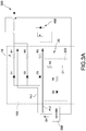
- FIG. 3A shows a schematic current diagram of turning-on the IGBT and the MOSFET of the hybrid drive circuit according to the present disclosure, and also refer to FIG. 1 to FIG. 2B .
- a first turn-on path Pc1 of the hybrid drive circuit 100 turns on the IGBT 300, and a second turn-on path Pc2 thereof turns on the MOSFET 400. Since the time of turning on the MOSFET 400 must be faster than that of turning on the IGBT 300, the resistance of the first resistor R1 must be greater than that of the third resistor R3. For example but not limited to that the first resistor R1 is 70 ohms and the third resistor R3 is 40 ohms.
- a time constant of the RC circuit composed of the first resistor R1 and the parasitic capacitance of the IGBT 300 is larger and the charge time is longer than those of the RC circuit composed of the third resistor R3 and the parasitic capacitance of the MOSFET 400. Since the difference in the charge time, a first delay time is generated between turning on the IGBT 300 by the first turn-on path Pc1 and turning on the MOSFET 400 by the second turn-on path Pc2, thereby providing the turn-on sequence shown in FIG. 2A .
- adjusting the parasitic capacitance by selecting the IGBT 300 or the MOSFET 400 is related to the charge time.
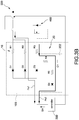
- FIG. 3B shows a schematic current diagram of turning-off the IGBT and the MOSFET of the hybrid drive circuit according to the present disclosure, and also refer to FIG. 1 to FIG. 2B .
- a first turn-off path Ps1 of the hybrid drive circuit 100 turns off the IGBT 300, and a second turn-off path Ps2 thereof turns off the MOSFET 400. Since the time of turning off the MOSFET 400 must be slower than that of turning off the IGBT 300, the sum resistance of the third resistor R3, the fourth resistor R4, and the fifth resistor R5 must be greater than that of the second resistor R2.
- the third resistor R3 is 40 ohms
- the fourth resistor R4 is 40 ohms
- the fifth resistor R5 is 50 ohms
- the second resistor R2 is 50 ohms. Therefore, only the second resistor R2 with a small resistance discharges and the discharge time is short when the IGBT 300 is turned off. Since the RC circuit composed of the third resistor R3, the fourth resistor R4, the fifth resistor R5, and the first capacitor C1 has a larger time constant, the discharge time thereof is longer comparing to the time constant of the second resistor R2 and the IGBT 300.
- a second delay time is generated between turning off the IGBT 300 by the first turn-off path Ps1 and turning off the MOSFET 400 by the second turn-off path Ps2, thereby providing the turn-off sequence shown in FIG. 2B .
- adjusting the resistance of the second resistor R2 that of the third resistor R3, that of the fourth resistor R4, or that of the fifth resistor R5
- adjusting the parasitic capacitance by selecting the IGBT 300 or the MOSFET 400 or the capacitance of the first capacitor C1 is related to the discharge time.
- the hybrid drive circuit 100' includes a first branch 10' and a second branch 20'.
- the first branch 10' is coupled to the IGBT 300 and the second branch 20' is coupled to the MOSFET 400.
- the first branch 10' includes a fifth diode D5, a sixth resistor R6, and a second capacitor C2.
- a cathode of the fifth diode D5 is coupled to the input signal Sin and an anode of the fifth diode D5 is coupled to the IGBT 300.
- the sixth resistor R6 is coupled to the fifth diode D5 coupled to the sixth resistor R6 in parallel.
- the second branch 20' includes a sixth diode D6, a seventh resistor R7, and a third capacitor C3.
- An anode of the sixth diode D6 is coupled to the input signal Sin, and a cathode of the sixth diode D6 is coupled to the MOSFET 400.
- a direction of the fifth diode D5 is different from that of the sixth diode D6.
- the seventh resistor R7 is coupled to the sixth diode D6.
- One end of the third capacitor C3 is coupled to the sixth diode D6, the seventh resistor R7, and the MOSFET 400, and the other end of the third capacitor C3 is coupled to the ground point.
- the sixth resistor R6 is a first turn-on path and the fifth diode D5 is a first turn-off path.
- the sixth diode D6 is a second turn-on path and the seventh resistor R7 is a second turn-off path.
- a first delay time is generated between turning on the IGBT 300 by the first turn-on path Pc1 and turning on the MOSFET 400 by the second turn-on path Pc2, thereby providing the turn-on sequence shown in FIG. 2A .
- adjusting the capacitance is related to the charge time.
- an RC circuit is composed of the seventh resistor R7 and the third capacitor C3, and the second capacitor C2 directly discharges. Therefore, a discharge time provided by the RC circuit (composed by the seventh resistor R7 and the third capacitor C3) is longer than a discharge time provided by the second capacitor C2. Since the difference in the discharge time, a second delay time is generated between turning off the IGBT 300 by the first turn-off path Ps1 and turning off the MOSFET 400 by the second turn-off path Ps2, thereby providing the turn-off sequence shown in FIG. 2B . In particular, besides adjusting the resistance, adjusting the capacitance is related to the discharge time.
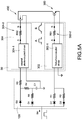
- FIG. 5A shows a circuit block diagram of the hybrid drive circuit having a photo-coupled drive module according to a third embodiment of the present disclosure, and also refer to FIG. 1 to FIG. 4 .
- An isolated component is used for the isolation of the drive circuit, and the isolated component may be a photo-coupled component, a capacitive-coupled component, or a magnetic-coupled component. For convenience, take the photo-coupled component for example.
- the hybrid drive circuit 100 includes a photo-coupled drive module 30.
- the photo-coupled drive module 30 is coupled between a first branch 10, a second branch 20, and an IGBT 300, a MOSFET 400.
- the photo-coupled drive module 30 includes a first photo-coupled drive circuit 302 and a second photo-coupled drive circuit 304.
- the first photo-coupled drive circuit 302 includes a first photo-coupled driver 302-1 and a first slope adjust circuit 302-2.
- the first photo-coupled driver 302-1 is coupled to the first branch 10
- the first slope adjust circuit 302-2 is coupled to the first photo-coupled driver 302-1 and the IGBT 300.
- the second photo-coupled drive circuit 304 includes second photo-coupled driver 304-1 and a second slope adjust circuit 304-2.
- the second photo-coupled driver 304-1 is coupled to the second branch 20, and the second slope adjust circuit 304-2 is coupled to the second photo-coupled driver 304-1 and the MOSFET 400.
- the first photo-coupled drive circuit 302 provides a first drive signal to the IGBT 300 according to a signal provided by the first branch 10
- the second photo-coupled drive circuit 304 provides a second drive signal to the MOSFET 400 according to a signal provided by the second branch 20.
- a first drive signal or a second drive signal acquired at an A point becomes a waveform (I) close to a square wave when a waveform having a slope passes through the first photo-coupled driver 302-1 and the second photo-coupled driver 304-1 shown in FIG. 2A and FIG. 2B so that the delay time of the IGBT 300 and the MOSFET 400 can be controlled without causing excessive losses due to the longer turn-on and turn-off time.
- the waveform (I) is close to the square wave with sharp rising edge and sharp falling edge, thus generating higher electromagnetic interference (EMI). Therefore, the first slope adjust circuit 302-2 and the second slope adjust circuit 304-2 are used to adjust the slope of the rising edge and that of the falling edge of the waveform (I) so that the first drive signal or the second drive signal acquired at a B point becomes a waveform (II) close to a trapezoidal wave. As shown in FIG. 5A , the first slope adjust circuit 302-2 and the second slope adjust circuit 304-2 are slope adjust resistors RS1, RS2, and the waveform (I) with sharp rising edge and sharp falling edge is adjusted to the waveform (II) with slow rising edge and slow falling edge.
- FIG. 5B shows a circuit block diagram of the hybrid drive circuit having the photo-coupled drive module according to a fourth embodiment of the present disclosure, and also refer to FIG. 1 to FIG. 5A .
- the photo-coupled drive module 30' in the former is coupled an input signal Sin, a first branch 10, and a second branch 20.
- a signal acquired at the A point is basically identical since the input signal Sin is identical, and therefore the delay effect is implemented when the signal acquired at the A point passes through the first branch 10 and the second branch 20.
- the difference in the position of the photo-coupled drive module 30 of FIG. 5A and that of 5B since the time of switching procedure by the first photo-coupled driver 302-1 and the second photo-coupled driver 304-1 is faster, the delay time is generated and the turn-on and turn-off are not extended when the photo-coupled drive module 30 is disposed at the position of FIG. 5A , thereby reducing unnecessary losses. Therefore, the photo-coupled drive module 30 is preferably disposed at the position of FIG. 5A , which can reduce the losses of the overall circuit.
- FIG. 6 shows a circuit block diagram of the photo-coupled drive module according to the present disclosure, and also refer to FIG. 1 to FIG. 5B .
- the first photo-coupled driver 302-1 and the second photo-coupled driver 304-1 includes a photo-coupled unit 306 and a drive unit 308, respectively.
- the photo-coupled unit 306 provides a high-level signal according to a rising edge rising (increasing) to a first trigger point, and provides a low-level signal according to a falling edge falling (decreasing) to a second trigger point.
- the photo-coupled unit 306 since the photo-coupled unit 306 has the characteristic of fast switching, the photo-coupled unit 306 quickly switches to be turned on when a voltage value of the rising edge gradually increases to a voltage value of the trigger point (the falling edge is also the same). Therefore, the photo-coupled unit 306 can adjust the rising or falling waveform to a sharp rising or sharp falling waveform. Since the photo-coupled unit 306 switches to be turned on or turned off when the rising edge or the falling edge reaches the trigger point, thereby causing a slight delay of the input waveform and the output waveform by the photo-coupled unit 306.
- the VCC is a drive voltage and the VEE is a reference ground voltage. Since the high-level signal provided by the photo-coupled unit 306 is not enough as the drive voltage VCC to drive the IGBT 300 or the MOSFET 400, the drive unit 308 needs to be used to provide the drive voltage VCC to drive the IGBT 300 or the MOSFET 400. When the signal provided by the photo-coupled unit 306 is high-level, the drive unit 308 provides the drive voltage VCC according to the high-level signal to turn on the IGBT 300 or the MOSFET 400.
- the drive unit 308 does not provide the drive voltage VCC according to the low-level signal to turn off the IGBT 300 or the MOSFET 400.
- the first photo-coupled driver 302-1 and the second photo-coupled driver 304-1 are, for example but not limited to, the photo-coupled driver (HCPL-3120) manufactured by Hewlett-Packard Company.
- both the first photo-coupled driver 302-1 and the second photo-coupled driver 304-1 can be replaced with a photo-coupled driver or other isolated drivers having the same effect.
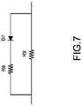
- FIG. 7 shows a circuit diagram of a slope adjust circuit according to the present disclosure, and also refer to FIG. 1 to FIG. 6 .
- the first slope adjust circuit 302-2 and the second slope adjust circuit 304-2 shown in FIG. 5A are slope adjust resistors RS1, RS2, respectively, and the slop adjust resistors RS1, RS2 can simultaneously adjust slopes of the rising edge and the falling edge of the waveform (I).
- the circuit structure is relatively simple, it is not possible to separately and independently adjust the slope of the rising edge and the slope of the falling edge.
- the first slope adjust circuit 302-2' and the second slope adjust circuit 304-2' shown in FIG. 7 can separately and independently adjust the slope of the rising edge and the slope of the falling edge.
- the first slope adjust circuit 302-2' or the second slope adjust circuit 304-2' includes an eighth resistor R8, a seventh diode D7, and a ninth resistor R9.
- a cathode of the seventh diode D7 is coupled to the eighth resistor R8 in series
- the ninth resistor R9 is coupled to the in-series eighth resistor R8 and the seventh diode D7 in parallel
- the ninth resistor R9 is coupled to an anode of the seventh diode D7.
- the first drive signal or the second drive signal passes through a rising-edge path composed by the ninth resistor R9
- the first drive signal or the second drive signal passes through a falling-edge path composed by the eighth resistor R8 and the seventh diode D7.
- the ninth resistor R9 adjusts the slope of the first rising edge or that slope of the second rising edge; when the first drive signal or the second drive signal passes through the falling-edge path, the eighth resistor R8 adjusts the slope of the first falling edge or the slope of the second falling edge.
- the ninth resistor R9 and the eighth resistor R8 can separately and independently adjust the slope of the rising edge and the slope of the falling edge, the designer can choose the appropriate slope of the rising edge and that of the falling edge according to the considerations of switching losses and electromagnetic interference.
- the resistance values of the ninth resistor R9 and the eighth resistor R8 may be different depending on the optimum design.
Landscapes
- Power Conversion In General (AREA)
- Electronic Switches (AREA)
Applications Claiming Priority (1)
| Application Number | Priority Date | Filing Date | Title |
|---|---|---|---|
| CN201910491216.5A CN112054791B (zh) | 2019-06-06 | 2019-06-06 | 混合驱动电路 |
Publications (1)
| Publication Number | Publication Date |
|---|---|
| EP3748852A1 true EP3748852A1 (fr) | 2020-12-09 |
Family
ID=68834981
Family Applications (1)
| Application Number | Title | Priority Date | Filing Date |
|---|---|---|---|
| EP19214202.4A Withdrawn EP3748852A1 (fr) | 2019-06-06 | 2019-12-06 | Circuit d'attaque hybride |
Country Status (4)
| Country | Link |
|---|---|
| US (1) | US10985752B2 (fr) |
| EP (1) | EP3748852A1 (fr) |
| JP (1) | JP7005664B2 (fr) |
| CN (1) | CN112054791B (fr) |
Families Citing this family (7)
| Publication number | Priority date | Publication date | Assignee | Title |
|---|---|---|---|---|
| JP6981393B2 (ja) * | 2018-10-26 | 2021-12-15 | オムロン株式会社 | スイッチング素子の駆動回路及びスイッチング回路 |
| CN112737286A (zh) * | 2021-01-04 | 2021-04-30 | 惠州市天宝创能科技有限公司 | 一种单端转双端的驱动电路及调节方法 |
| CN114900160A (zh) * | 2022-04-13 | 2022-08-12 | 中国电子科技集团公司第二十四研究所 | 驱动信号产生电路及方法 |
| JP2024135239A (ja) * | 2023-03-22 | 2024-10-04 | 株式会社東芝 | 高周波半導体集積回路 |
| US12381473B2 (en) * | 2023-10-24 | 2025-08-05 | Infineon Technologies Canada Inc. | Driver circuit for a power transistor |
| CN117543966A (zh) * | 2023-11-08 | 2024-02-09 | 台达电子企业管理(上海)有限公司 | 功率开关电路及其控制方法 |
| WO2026042706A1 (fr) * | 2024-08-22 | 2026-02-26 | ローム株式会社 | Circuit de génération de signal de commande, dispositif de conversion d'énergie électrique et véhicule |
Citations (3)
| Publication number | Priority date | Publication date | Assignee | Title |
|---|---|---|---|---|
| US20150028383A1 (en) * | 2013-07-25 | 2015-01-29 | Infineon Technologies Ag | Power MOS Transistor with Integrated Gate-Resistor |
| WO2016014907A1 (fr) * | 2014-07-24 | 2016-01-28 | Eaton Corporation | Procédés et systèmes pour le fonctionnement de dispositifs de puissance hybride au moyen de circuit d'attaque qui exécutent une détection de courant de charge instantanée indirecte |
| US20180316342A1 (en) * | 2017-04-26 | 2018-11-01 | Futurewei Technologies, Inc. | Hybrid Power Devices |
Family Cites Families (19)
| Publication number | Priority date | Publication date | Assignee | Title |
|---|---|---|---|---|
| US4404474A (en) * | 1981-02-06 | 1983-09-13 | Rca Corporation | Active load pulse generating circuit |
| US7312626B2 (en) * | 2005-08-31 | 2007-12-25 | Micron Technology, Inc. | CMOS circuits with reduced crowbar current |
| CN101378254B (zh) * | 2007-08-31 | 2010-11-24 | 深圳市圣美歌科技有限公司 | 高速开关管浮动栅极驱动电路 |
| JP5119894B2 (ja) * | 2007-12-06 | 2013-01-16 | 富士電機株式会社 | ドライバ回路 |
| US7940503B2 (en) | 2008-05-27 | 2011-05-10 | Infineon Technologies Ag | Power semiconductor arrangement including conditional active clamping |
| CN101786412A (zh) * | 2009-12-31 | 2010-07-28 | 江苏常隆客车有限公司 | 同时控制混合动力汽车电机和dc-dc电源的控制系统 |
| EP2587670A1 (fr) * | 2011-10-26 | 2013-05-01 | ABB Technology AG | Système de commande pour contrôler les contacts |
| CN203590014U (zh) * | 2013-09-29 | 2014-05-07 | 深圳市伟创电气有限公司 | 小功率igbt驱动互锁电路 |
| US9573474B2 (en) * | 2014-03-06 | 2017-02-21 | Ford Global Technologies, Llc | Capacitor precharging and capacitance/resistance measurement in electric vehicle drive system |
| JP6402591B2 (ja) * | 2014-10-31 | 2018-10-10 | 富士電機株式会社 | 半導体装置 |
| JP6398872B2 (ja) * | 2015-05-27 | 2018-10-03 | 株式会社デンソー | 駆動装置 |
| KR101970112B1 (ko) * | 2015-08-07 | 2019-04-17 | 미쓰비시덴키 가부시키가이샤 | 파워 스위칭 장치 |
| CN105846813B (zh) * | 2016-05-24 | 2018-11-13 | 深圳芯能半导体技术有限公司 | 高压驱动电路的滤波电路和高压驱动电路 |
| JP6512193B2 (ja) * | 2016-08-17 | 2019-05-15 | 株式会社デンソー | トランジスタ駆動回路 |
| US10644689B2 (en) * | 2016-08-17 | 2020-05-05 | Denso Corporation | Transistor drive circuit and motor drive control apparatus |
| US10525841B2 (en) | 2016-10-12 | 2020-01-07 | Ford Global Technologies, Llc | Gate driver with short circuit protection |
| KR101841159B1 (ko) * | 2016-12-22 | 2018-03-22 | 주식회사 윌링스 | 스위칭 게이트 드라이브 |
| CN106849621B (zh) * | 2017-01-03 | 2019-05-28 | 昂宝电子(上海)有限公司 | 一种实现栅极驱动电路的系统和方法 |
| CN109698608A (zh) * | 2018-12-21 | 2019-04-30 | 江苏固德威电源科技股份有限公司 | 一种开关器件及其采用的控制方法 |
-
2019
- 2019-06-06 CN CN201910491216.5A patent/CN112054791B/zh active Active
- 2019-12-06 EP EP19214202.4A patent/EP3748852A1/fr not_active Withdrawn
- 2019-12-13 US US16/713,997 patent/US10985752B2/en active Active
-
2020
- 2020-02-21 JP JP2020027739A patent/JP7005664B2/ja active Active
Patent Citations (3)
| Publication number | Priority date | Publication date | Assignee | Title |
|---|---|---|---|---|
| US20150028383A1 (en) * | 2013-07-25 | 2015-01-29 | Infineon Technologies Ag | Power MOS Transistor with Integrated Gate-Resistor |
| WO2016014907A1 (fr) * | 2014-07-24 | 2016-01-28 | Eaton Corporation | Procédés et systèmes pour le fonctionnement de dispositifs de puissance hybride au moyen de circuit d'attaque qui exécutent une détection de courant de charge instantanée indirecte |
| US20180316342A1 (en) * | 2017-04-26 | 2018-11-01 | Futurewei Technologies, Inc. | Hybrid Power Devices |
Also Published As
| Publication number | Publication date |
|---|---|
| US20200389168A1 (en) | 2020-12-10 |
| CN112054791B (zh) | 2023-11-21 |
| US10985752B2 (en) | 2021-04-20 |
| CN112054791A (zh) | 2020-12-08 |
| JP7005664B2 (ja) | 2022-01-21 |
| JP2020202552A (ja) | 2020-12-17 |
Similar Documents
| Publication | Publication Date | Title |
|---|---|---|
| EP3748852A1 (fr) | Circuit d'attaque hybride | |
| CN102769451B (zh) | 半导体装置及电子设备 | |
| JP4763606B2 (ja) | 半導体スイッチの高周波制御 | |
| US11543846B2 (en) | Gate driver circuit for reducing deadtime inefficiencies | |
| EP3890190A1 (fr) | Circuit d'attaque de grille à perte de conduction de semi-conducteur de puissance réduite | |
| US20120268091A1 (en) | Switching circuit device and power supply device having same | |
| CN114050712B (zh) | 栅极驱动装置及方法 | |
| KR20130011812A (ko) | Igbt 구동 방법 | |
| WO2010134276A1 (fr) | Circuit d'attaque de la grille | |
| KR20090014402A (ko) | 스위칭 회로 장치 | |
| CN101335483A (zh) | 电力变换装置 | |
| KR102744915B1 (ko) | 전류 가변 mosfet 게이트 구동회로 | |
| KR102026929B1 (ko) | 전력 스위치용 게이트 구동회로 | |
| Frank | Simple slew-rate control technique cuts switching losses | |
| CN113796010A (zh) | 功率半导体的适应性开关速度控制 | |
| JP7749979B2 (ja) | 駆動装置 | |
| TWI504119B (zh) | 防止寄生元件導通之裝置及其方法 | |
| TWI676355B (zh) | 混合驅動電路 | |
| US12603647B2 (en) | Driver circuit of switching transistor, laser driver circuit, and controller circuit of converter | |
| CN114696595A (zh) | 驱动装置 | |
| JP4830829B2 (ja) | 絶縁ゲートトランジスタの駆動回路 | |
| JP2022027042A (ja) | ゲート駆動回路および電源回路 | |
| KR20250160798A (ko) | 하이브리드 스위치를 구동시키기 위한 시스템 | |
| JP2008259031A (ja) | 負荷駆動装置 | |
| JP2016082335A (ja) | 半導体装置 |
Legal Events
| Date | Code | Title | Description |
|---|---|---|---|
| PUAI | Public reference made under article 153(3) epc to a published international application that has entered the european phase |
Free format text: ORIGINAL CODE: 0009012 |
|
| STAA | Information on the status of an ep patent application or granted ep patent |
Free format text: STATUS: THE APPLICATION HAS BEEN PUBLISHED |
|
| AK | Designated contracting states |
Kind code of ref document: A1 Designated state(s): AL AT BE BG CH CY CZ DE DK EE ES FI FR GB GR HR HU IE IS IT LI LT LU LV MC MK MT NL NO PL PT RO RS SE SI SK SM TR |
|
| AX | Request for extension of the european patent |
Extension state: BA ME |
|
| STAA | Information on the status of an ep patent application or granted ep patent |
Free format text: STATUS: THE APPLICATION IS DEEMED TO BE WITHDRAWN |
|
| 18D | Application deemed to be withdrawn |
Effective date: 20210610 |