EP3748948B1 - Module de caméra, procédé d'assemblage de module de caméra et terminal mobile - Google Patents
Module de caméra, procédé d'assemblage de module de caméra et terminal mobile Download PDFInfo
- Publication number
- EP3748948B1 EP3748948B1 EP19747844.9A EP19747844A EP3748948B1 EP 3748948 B1 EP3748948 B1 EP 3748948B1 EP 19747844 A EP19747844 A EP 19747844A EP 3748948 B1 EP3748948 B1 EP 3748948B1
- Authority
- EP
- European Patent Office
- Prior art keywords
- chip
- protective layer
- camera module
- connection wire
- protective
- Prior art date
- Legal status (The legal status is an assumption and is not a legal conclusion. Google has not performed a legal analysis and makes no representation as to the accuracy of the status listed.)
- Active
Links
Images

Classifications
-
- H—ELECTRICITY
- H04—ELECTRIC COMMUNICATION TECHNIQUE
- H04N—PICTORIAL COMMUNICATION, e.g. TELEVISION
- H04N23/00—Cameras or camera modules comprising electronic image sensors; Control thereof
- H04N23/50—Constructional details
-
- H—ELECTRICITY
- H04—ELECTRIC COMMUNICATION TECHNIQUE
- H04N—PICTORIAL COMMUNICATION, e.g. TELEVISION
- H04N23/00—Cameras or camera modules comprising electronic image sensors; Control thereof
- H04N23/50—Constructional details
- H04N23/51—Housings
-
- H—ELECTRICITY
- H04—ELECTRIC COMMUNICATION TECHNIQUE
- H04M—TELEPHONIC COMMUNICATION
- H04M1/00—Substation equipment, e.g. for use by subscribers
- H04M1/02—Constructional features of telephone sets
- H04M1/0202—Portable telephone sets, e.g. cordless phones, mobile phones or bar type handsets
- H04M1/026—Details of the structure or mounting of specific components
- H04M1/0264—Details of the structure or mounting of specific components for a camera module assembly
-
- H—ELECTRICITY
- H04—ELECTRIC COMMUNICATION TECHNIQUE
- H04N—PICTORIAL COMMUNICATION, e.g. TELEVISION
- H04N23/00—Cameras or camera modules comprising electronic image sensors; Control thereof
- H04N23/50—Constructional details
- H04N23/54—Mounting of pick-up tubes, electronic image sensors, deviation or focusing coils
-
- H—ELECTRICITY
- H04—ELECTRIC COMMUNICATION TECHNIQUE
- H04N—PICTORIAL COMMUNICATION, e.g. TELEVISION
- H04N23/00—Cameras or camera modules comprising electronic image sensors; Control thereof
- H04N23/57—Mechanical or electrical details of cameras or camera modules specially adapted for being embedded in other devices
-
- H—ELECTRICITY
- H05—ELECTRIC TECHNIQUES NOT OTHERWISE PROVIDED FOR
- H05K—PRINTED CIRCUITS; CASINGS OR CONSTRUCTIONAL DETAILS OF ELECTRIC APPARATUS; MANUFACTURE OF ASSEMBLAGES OF ELECTRICAL COMPONENTS
- H05K1/00—Printed circuits
- H05K1/18—Printed circuits structurally associated with non-printed electric components
- H05K1/189—Printed circuits structurally associated with non-printed electric components characterised by the use of flexible or folded printed circuits
-
- H—ELECTRICITY
- H05—ELECTRIC TECHNIQUES NOT OTHERWISE PROVIDED FOR
- H05K—PRINTED CIRCUITS; CASINGS OR CONSTRUCTIONAL DETAILS OF ELECTRIC APPARATUS; MANUFACTURE OF ASSEMBLAGES OF ELECTRICAL COMPONENTS
- H05K3/00—Apparatus or processes for manufacturing printed circuits
- H05K3/22—Secondary treatment of printed circuits
- H05K3/28—Applying non-metallic protective coatings
- H05K3/284—Applying non-metallic protective coatings for encapsulating mounted components
-
- H—ELECTRICITY
- H10—SEMICONDUCTOR DEVICES; ELECTRIC SOLID-STATE DEVICES NOT OTHERWISE PROVIDED FOR
- H10F—INORGANIC SEMICONDUCTOR DEVICES SENSITIVE TO INFRARED RADIATION, LIGHT, ELECTROMAGNETIC RADIATION OF SHORTER WAVELENGTH OR CORPUSCULAR RADIATION
- H10F39/00—Integrated devices, or assemblies of multiple devices, comprising at least one element covered by group H10F30/00, e.g. radiation detectors comprising photodiode arrays
- H10F39/80—Constructional details of image sensors
- H10F39/804—Containers or encapsulations
Definitions
- the present disclosure relates to the technical field of communications, in particular to a camera module, a method for assembling the camera module, and a mobile terminal.
- the thickness of the mobile phone has become thinner and thinner, and the space available for a camera module inside the mobile phone has become smaller and smaller. Therefore, it is required to reduce the size of the camera module.
- a camera lens holder inside the camera module is omitted to achieve the effect of reducing the thickness of the camera.
- plastics C are injected to the periphery of the gold wire B through a plastic injection mold D to ensure that the gold wire B is not exposed.
- a problem in the related art lies in that when plastic injection molding is performed, because a contact area between the plastic injection mold D and a chip A is small (at a positon E in FIG.
- a force bearing area on the chip A for withstanding a pressure exerted by the plastic injection mold D is small, which may easily cause the chip A to be cracked at a positon of the chip A in direct contact with the plastic injection mold D, after being subjected to a relatively large pressure, thereby causing a failure to the entire camera module.
- Document " US2017271390" discussed a camera module and array camera module with circuit board unit and photosensitive unit and manufacturing method thereof is provided.
- the array camera module comprises two or more camera lenses and a circuit unit.
- the circuit unit comprises a circuit board portion for electrically connecting two or more photosensitive sensors of the array camera module, and a conjoined encapsulation portion integrally encapsulated on the circuit board portion.
- the camera lenses are respectively arranged along the photosensitive paths of the photosensitive sensors.
- Document " US2009166784” discussed a transparent plate which is supported by the gold bumps and is made to adhere over the solid imaging device by the adhesive.
- the gold bumps and an electrode and wiring pattern formed over a circuit board are connected by gold wires.
- the gold wires are approximately parallel to the circuit board near portions where the gold wires and the gold bumps are connected.
- the adhesive By locating the adhesive over the portions where the gold wires and the gold bumps are connected, the solid imaging device can be made small and light. As a result, a smaller lighter semiconductor device is fabricated.
- US2008246854 discussed an exemplary camera module which includes a lens holder, a lens module, a lens module, an image sensor chip, and an attaching member.
- the lens module is received in the lens holder.
- the lens module comprises a barrel and at least one lens received in the barrel.
- the image sensor chip comprises a photosensitive area configured for receiving light transmitted through the lens module.
- the attaching member is disposed at an end portion of the lens holder opposite to the lens module.
- the attaching member is configured for attaching the lens holder to the image sensor chip.
- the attaching member defines a light transmittance space configured for exposing the photosensitive area to the lens module.
- Embodiments of the present disclosure provide a camera module, a method for assembling the camera module and a mobile terminal, to solve a problem that a chip is cracked or a failure occurs to a camera module due to a small contact area between a plastic injection mold and the chip. Scope of the present invention is determined only by the scope of the appended claims and corresponds to the amended set of claims.
- the contact area with the chip is increased, so that a force bearing area on the chip for withstanding a pressure applied by a plastic injection mold is increased, which can prevent the chip from being cracked and ensure the camera to operate normally.
- the camera module includes: a flexible circuit board 1; a chip 2, stacked on the flexible circuit board 1; an image sensor 3, stacked on the chip 2; a connection wire 4, where one end of the connection wire 4 is connected to a wiring region of the flexible circuit board 1, the other end of the connection wire 4 is connected to an interface region of a first surface of the chip 2, and the first surface is a surface of the chip 2 away from the flexible circuit board 1; and a first protective structure 5, arranged on the interface region of the first surface of the chip. A portion of the connection wire 4 protruding in a direction away from the first surface is located inside the first protective structure 5.
- the first protective structure 5 is added in the camera module, a contact area with the chip 2 is increased, so that a force bearing area on the chip 2 for withstanding a pressure applied by a plastic injection mold is increased, which can prevent the chip 2 from being cracked and ensure the camera to operate normally. Additionally, since a camera lens holder is eliminated, the size of the camera module becomes smaller, which achieves the effect of reducing the thickness of the mobile terminal.
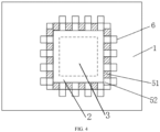
- the number of the connection wires 4 is plural, the first protective structure 5 is formed as a frame-shaped structure on the first surface of the chip 2, and a portion of each of the plurality of connection wires 4 protruding in a direction away from the first surface is located inside the first protective structure 5.
- the image sensor 3 is exposed from a hollow part of the first protective structure 5, so that a light ray collected by a camera lens of the camera module can be projected to the image sensor 3, the image sensor 3 converts an optical signal into an electrical signal, and an image is further formed by the chip 2.
- the camera module further includes: a second protective structure 6, arranged in the wiring region on the flexible circuit board 1, and a portion of the connection wire 4 protruding in a direction away from a side surface of the chip 2 is arranged inside the second protective structure 6.
- the second protective structure 6 is made of plastic, which is formed by injection-molding plastics through a plastic injection mold arranged on the first protective structure 5 to the portion of the connection wire 4 protruding in the direction away from the side surface of the chip 2.
- the second protective structure 6 is arranged in close contact with the side surface of the chip 2. As shown in FIG. 2 , in an embodiment of the present disclosure, the second protective structure 6 is a cuboid-shaped structure.
- the first protective structure 5 clads the portion of the connection wire 4 protruding in the direction away from the first surface
- the second protective structure 6 clads a portion of the connection wire 4 protruding in the direction away from the side surface of the chip 2, so that the connection wire 4 will not be exposed. Therefore, the camera lens holder in the camera module can be omitted, and the size of the camera module can be decreased while ensuring a failure not to occur to a connection between the connection wire 4 and the chip 2 or a connection between the connection wire 4 and the flexible circuit board 1.
- the first protective structure 5 and the second protective structure 6 are snugly connected.
- the second protective structure 6 is injection-molded on the flexible circuit board 1 by using a plastic injection molding process, after the second protective structure 6 is injection-molded on the flexible circuit board 1, the second protective structure 6 is attached to the first protective structure 5, so as to achieve a fixed connection between the two structures.
- the first protective structure 5 and the second protective structure 6 are snugly connected, so that the connection wire 4 can be completely surrounded.
- a surface of the second protective structure 6 away from the flexible circuit board 1 and a surface of the first protective structure 5 away from the chip 2 are located on a same surface.
- the surface of the second protective structure 6 away from the flexible circuit board 1 and the surface of the first protective structure 5 away from the chip 2 are arranged on the same surface, which facilitates the installation of a camera lens of the camera module.
- a predetermined distance is provided between an orthographic projection of the first protective structure 5 onto the chip 2 and an orthographic projection of the image sensor 3 onto the chip 2.
- Such setting is to prevent the image sensor 3 from being pressed by the plastic injection mold during the plastic injection molding of the second protective structure 6 to cause the image sensor 3 to be broken, so as to ensure the structural integrity of the image sensor 3.
- a side surface of the first protective structure 5 away from the image sensor 3 and the side surface of the chip 2 away from the image sensor 3 are located on a same surface.
- the side surface of the first protective structure 5 away from the image sensor 3 and the side surface of the chip 2 away from the image sensor 3 are arranged on the same surface, which facilitates the plastic injection molding of the second protective structure 6.
- the first protective structure 5 may be arranged on the first surface of the chip 2 in two ways.
- the first protective structure 5 in the first arrangement includes: a first protective layer 51 arranged on the first surface of the chip 2, where the portion of the connection wire 4 protruding in a direction away from the first surface is located inside the protective layer 51; and a second protective layer 52 attached onto a surface of the first protective layer 51 away from the chip 2.
- a hardness of the second protective layer 52 is larger than a hardness of the first protective layer 51.
- the second protective layer 52 is made of ceramic material, silicon material, resin substrate material or epoxy glass fiber board material, and the first protective layer 51 is a double-sided adhesive.
- a material grade corresponding to the epoxy glass fiber board is FR4.
- the first protective layer 51 is the double-sided adhesive, and a thickness of the double-sided adhesive is greater than a height of the portion of the connection wire 4 that protrudes in the direction away from the first surface, so as to ensure that the double-sided adhesive can clad the portion of the connection wire 4 protruding in the direction away from the first surface.
- the first protective layer 51 and the second protective layer 52 may be a frame-shaped structure, the image sensor 3 is exposed from a hollow part of the first protective layer 51 and the second protective layer 52, so that a light ray collected by a camera lens of the camera module can be projected to the image sensor 3.
- the first protective layer 51 may be constructed as a frame-shaped structure
- the second protective layer 52 may be constructed as a cuboid-shaped structure.
- the number of the second protective layers 52 may be multiple, the multiple second protective layers 52 are evenly stacked on the first protective layer 51, and the multiple second protective layers 52 are distributed around a center line of the frame-shaped structure.
- the multiple connection wires 4 are respectively cladded inside the first protective layer 51.
- the second protective layer 52 may be constructed as a frame-shaped structure, and the first protective layer 51 may be constructed as a cuboid-shaped structure.
- the number of the first protective layers 51 may be multiple, and the multiple first protective layers 51 are distributed around a center line of the frame-shaped structure, the second protective layer 52 is stacked on the multiple first protective layers 51, and each of the connection wires 4 corresponds to one of the first protective layers 51.
- the second protective structure 6 is attached to the first protective layer 51 and the second protective layer 52.
- a surface of the second protective structure 6 away from the flexible circuit board 1 and a surface of the second protective layer 52 away from the chip 2 are located on a same surface.
- a side surface of the first protective layer 51 facing a side surface of the image sensor 3 and a side surface of the second protective layer 52 facing the side surface of the image sensor 3 are located on a same surface.
- a side surface of the first protective layer 51 away from the side surface of the image sensor 3 and a side surface of the second protective layer 52 away from the side surface of the image sensor 3 are located on a same surface.
- connection wire 4 By arranging the portion of each connection wire 4 protruding in the direction away from the first surface inside the first protective layer 51, the connection wire 4 can be prevented from being exposed, and the connection wire 4 can be ensured to be fixedly connected to a welding spot of the chip 2. Additionally, since the second protective layer 52 arranged on the first protective layer 51 increases the contact area with the chip 2, the force bearing area on the chip 2 for withstanding a pressure applied by a plastic injection mold increases, thereby avoiding the problem that the chip 2 is cracked and ensuring the camera to operate normally.
- the first protective structure 5 in the second arrangement includes: a first protective layer 51 arranged on the first surface of the chip 2, where the portion of the connection wire 4 protruding in a direction away from the first surface is located inside the protective layer 51; and a second protective layer 52 arranged on the first surface of the chip 2, where a surface of the second protective layer 52 away from the chip 2 is located above a surface of the first protection layer 51 away from the chip 2.
- a hardness of the second protective layer 52 is larger than a hardness of the first protective layer 51.
- the second protective layer 52 is made of ceramic material, silicon material, resin substrate material, or epoxy glass fiber board material, where a material grade corresponding to the epoxy glass fiber board is FR4.
- the first protective layer 51 may be a structure made of a flexible material such as plastic.
- each of the first protective structure 5 and the second protective structure 6 is a cuboid-shaped structure.
- the side surface of the first protective layer 51 and the side surface of the second protective layer 52 may be attached to each other, or may not be attached.
- That the surface of the second protective layer 52 away from the chip 2 is located above the surface of the first protective layer 51 away from the chip 2 means that a height of the first protective layer 51 is lower than a height of the second protective layer 52. In such manner, it can be ensured that when the second injection structure 6 is injection-molded by using a plastic injection mold, the first protective layer 51 cannot contact the plastic injection mold.
- the second protective structure 6 is attached to the first protective layer 51 and the second protective layer 52.
- a surface of the second protective structure 6 away from the flexible circuit board 1 and a surface of the second protective layer 52 away from the chip 2 are located on a same surface.
- a side surface of the first protective layer 51 facing a side surface of the image sensor 3 and a side surface of the second protective layer 52 facing the side surface of the image sensor 3 are located on a same surface.
- a side surface of the first protective layer 51 away from the side surface of the image sensor 3 and a side surface of the second protective layer 52 away from the side surface of the image sensor 3 are located on a same surface.
- connection wire 4 By arranging the portion of each connection wire 4 protruding in the direction away from the first surface inside the first protective layer 51, the connection wire 4 can be prevented from being exposed, and the connection wire 4 can be ensured to be fixedly connected to a welding spot of the chip 2. Additionally, since the second protective layer 52 provided on the first protective layer 51 increases the contact area with the chip 2, the force bearing area on the chip 2 for withstanding a pressure applied by a plastic injection mold increases, thereby avoiding the problem that the chip 2 is cracked and ensuring the camera to operate normally.
- an embodiment of the present disclosure further provides a mobile terminal, including the above camera module.
- the contact area with the chip 2 is increased, so that a force bearing area on the chip 2 for withstanding a pressure applied by a plastic injection mold is increased, which can prevent the chip 2 from being cracked and ensure the camera to operate normally.
- the present disclosure further provides a method for assembling a camera module, including:
- the contact area with the chip 2 is increased, so that the force bearing area on the chip 2 for withstanding a pressure applied by a plastic injection mold increases, thereby avoiding the problem that the chip 2 is cracked and ensuring the camera to operate normally.
- the second protective structure 6 is injection-molded, with a plastic injection mold, on the portion of the connection wire 4 protruding in a direction away from a side surface of the chip 2, such that the second protective structure 6 is snugly connected to a surface of the flexible circuit board 1 arranged with the chip 2, and a portion of the connection wire 4 protruding in a direction away from the side surface of the chip 2 is arranged inside the second protective structure 6.
- the first protective structure 5 clads the portion of the connection wire 4 protruding in the direction away from the first surface
- the second protective structure 6 clads the portion of the connection wire 4 protruding in the direction away from the side surface of the chip 2, so that the connection wire 4 will not be exposed. Therefore, the camera lens holder in the camera module can be omitted, and the size of the camera module can be decreased while ensuring a failure not to occur to a connection between the connection wire 4 and the chip 2 or a connection between the connection wire 4 and the flexible circuit board 1.
Landscapes
- Engineering & Computer Science (AREA)
- Signal Processing (AREA)
- Multimedia (AREA)
- Microelectronics & Electronic Packaging (AREA)
- Manufacturing & Machinery (AREA)
- Studio Devices (AREA)
- Camera Bodies And Camera Details Or Accessories (AREA)
- Transforming Light Signals Into Electric Signals (AREA)
- Solid State Image Pick-Up Elements (AREA)
Claims (9)
- Module de caméra, comprenant :une carte de circuit imprimé flexible (1) ;une puce (2), placée sur la carte de circuit imprimé flexible (1) ;un capteur d'images (3), placé sur la puce (2) ;un fil de connexion (4), dans lequel une extrémité du fil de connexion (4) est raccordée à une zone de câblage de la carte de circuit imprimé flexible (1), l'autre extrémité du fil de connexion (4) est raccordée à une zone d'interface d'une première surface de la puce (2), et la première surface est une surface de la puce (2) éloignée de la carte de circuit imprimé flexible (1) ;une première structure de protection (5), disposée sur la zone d'interface de la première surface de la puce (2) ;dans lequel une partie du fil de connexion (4) dépassant dans une direction opposée à la première surface est située à l'intérieur de la première structure de protection (5) ;caractérisé en ce que la première structure de protection (5) comprend :une première couche de protection (51), disposée sur la première surface de la puce (2), dans lequel la partie du fil de connexion (4) dépassant dans la direction opposée à la première surface est située à l'intérieur de la première couche de protection ; etune seconde couche de protection (52), fixée sur une surface de la première couche de protection éloignée de la puce (2),dans lequel une dureté de la seconde couche de protection est supérieure à celle de la première couche de protection ;le module de caméra comprend en outre une seconde structure de protection (6) disposée dans la zone de câblage sur la carte de circuit flexible (1) ;une surface latérale de la première couche de protection (51) faisant face à une surface latérale du capteur d'images (3) et une surface latérale de la seconde couche de protection (52) faisant face à la surface latérale du capteur d'images (3) sont situées sur une même surface ; etune distance prédéterminée est prévue entre une projection orthographique de la première couche de protection (51) sur la puce (2) et une projection orthographique du capteur d'image (3) sur la puce (2), et entre une projection orthographique de la seconde couche de protection (52) sur la puce (2) et la projection orthographique du capteur d'image (3) sur la puce (2).
- Module de caméra selon la revendication 1, dans lequel la seconde couche de protection (52) est constituée d'un matériau céramique, d'un matériau siliconé, d'un matériau de substrat en résine ou d'un matériau de panneau de fibre de verre époxy, et la première couche de protection est un adhésif double face.
- Module de caméra selon la revendication 1,
dans lequel une surface de la seconde couche de protection (52) éloignée de la puce (2) est située au-dessus d'une surface de la première couche de protection (51) éloignée de la puce (2), et une dureté de la seconde couche de protection (52) est supérieure à une dureté de la première couche de protection (51). - Module de caméra selon la revendication 1, dans lequel une partie du fil de connexion (4) dépassant dans une direction opposée à une surface latérale de la puce (2) est disposée à l'intérieur de la seconde structure de protection (6).
- Module de caméra selon la revendication 4, dans lequel une surface de la seconde structure de protection éloignée de la carte de circuit imprimé flexible (1) et une surface de la première structure de protection (5) éloignée de la puce (2) sont sur une même surface.
- Module de caméra selon la revendication 1, dans lequel le nombre de fils de connexion (4) est pluriel, la première structure de protection (5) est formée comme une structure en forme de cadre sur la première surface de la puce (2), et une partie de chaque fil de connexion (4) dépassant dans une direction éloignée de la première surface est située à l'intérieur de la première structure de protection (5).
- Terminal mobile, comprenant le module de caméra selon l'une quelconque des revendications 1 à 6.
- Procédé d'assemblage d'un module de caméra, appliqué au module de caméra selon l'une quelconque des revendications 1 à 6, comprenant :la mise en place de la puce (2) sur le circuit imprimé flexible (1) ;la mise en place du capteur d'images (3) sur la puce (2) ;le raccordement d'une extrémité du fil de connexion (4) à la carte de circuit imprimé flexible (1) et de l'autre extrémité du fil de connexion (4) à la première surface de la puce (2) ;la disposition de la première structure de protection (5) sur la première surface de la puce (2), afin de permettre à une partie du fil de connexion (4) dépassant dans une direction opposée à la première surface d'être située à l'intérieur de la première structure de protection (5) ; etle moulage par injection, à l'aide d'un moule d'injection plastique, d'une seconde structure de protection (6) sur la partie du fil de connexion (4) dépassant dans une direction opposée à une surface latérale de la puce (2).
- Procédé d'assemblage d'un module de caméra selon la revendication 8, dans lequel la seconde structure de protection (6) est étroitement raccordée à une surface de la carte de circuit flexible (1) disposée avec la puce (2), et une partie du fil de connexion (4) dépassant dans une direction opposée à la surface latérale de la puce (2) est disposée à l'intérieur de la seconde structure de protection (6).
Applications Claiming Priority (2)
| Application Number | Priority Date | Filing Date | Title |
|---|---|---|---|
| CN201810090181.XA CN108134898B (zh) | 2018-01-30 | 2018-01-30 | 一种摄像头模组、摄像头模组的组装方法及移动终端 |
| PCT/CN2019/073169 WO2019149149A1 (fr) | 2018-01-30 | 2019-01-25 | Module de caméra, procédé d'assemblage de module de caméra et terminal mobile |
Publications (3)
| Publication Number | Publication Date |
|---|---|
| EP3748948A1 EP3748948A1 (fr) | 2020-12-09 |
| EP3748948A4 EP3748948A4 (fr) | 2021-02-24 |
| EP3748948B1 true EP3748948B1 (fr) | 2024-11-06 |
Family
ID=62430095
Family Applications (1)
| Application Number | Title | Priority Date | Filing Date |
|---|---|---|---|
| EP19747844.9A Active EP3748948B1 (fr) | 2018-01-30 | 2019-01-25 | Module de caméra, procédé d'assemblage de module de caméra et terminal mobile |
Country Status (7)
| Country | Link |
|---|---|
| US (1) | US11297210B2 (fr) |
| EP (1) | EP3748948B1 (fr) |
| JP (1) | JP7150860B2 (fr) |
| KR (1) | KR102355287B1 (fr) |
| CN (1) | CN108134898B (fr) |
| ES (1) | ES2994605T3 (fr) |
| WO (1) | WO2019149149A1 (fr) |
Families Citing this family (6)
| Publication number | Priority date | Publication date | Assignee | Title |
|---|---|---|---|---|
| CN108134898B (zh) * | 2018-01-30 | 2020-04-10 | 维沃移动通信有限公司 | 一种摄像头模组、摄像头模组的组装方法及移动终端 |
| CN112038301A (zh) * | 2019-06-03 | 2020-12-04 | 华为技术有限公司 | 芯片、电子器件及芯片的制作方法 |
| CN111836462B (zh) * | 2020-08-03 | 2022-02-01 | Oppo广东移动通信有限公司 | 穿戴式设备 |
| CN115404130B (zh) * | 2022-09-02 | 2023-09-05 | 无锡锡州机械有限公司 | 一种热交换器加工工艺 |
| WO2024053888A1 (fr) * | 2022-09-08 | 2024-03-14 | 삼성전자주식회사 | Module de prise de vues et appareil électronique le comprenant |
| CN115499570B (zh) * | 2022-09-14 | 2024-04-16 | 昆山丘钛微电子科技股份有限公司 | 一种摄像头模组的封装方法及装置 |
Family Cites Families (31)
| Publication number | Priority date | Publication date | Assignee | Title |
|---|---|---|---|---|
| EP1471730A1 (fr) | 2003-03-31 | 2004-10-27 | Dialog Semiconductor GmbH | Module miniature avec caméra |
| JP2005079499A (ja) * | 2003-09-03 | 2005-03-24 | Seiko Epson Corp | 半導体装置、半導体モジュール、電子機器および半導体装置の製造方法 |
| KR100592368B1 (ko) | 2004-07-06 | 2006-06-22 | 삼성전자주식회사 | 반도체 소자의 초박형 모듈 제조 방법 |
| KR20070096303A (ko) * | 2006-03-23 | 2007-10-02 | 엘지이노텍 주식회사 | 카메라 모듈용 인쇄회로기판 및 그 제조 방법 |
| CN100514589C (zh) | 2006-05-09 | 2009-07-15 | 探微科技股份有限公司 | 晶圆级封装方法及其结构 |
| KR101100790B1 (ko) | 2006-09-15 | 2012-01-02 | 후지쯔 세미컨덕터 가부시키가이샤 | 반도체 장치 및 그 제조 방법 |
| US20080191335A1 (en) | 2007-02-08 | 2008-08-14 | Advanced Chip Engineering Technology Inc. | Cmos image sensor chip scale package with die receiving opening and method of the same |
| CN101281284A (zh) | 2007-04-04 | 2008-10-08 | 鸿富锦精密工业(深圳)有限公司 | 相机模组 |
| CN100561280C (zh) | 2007-05-30 | 2009-11-18 | 鸿富锦精密工业(深圳)有限公司 | 相机模组及其制造方法 |
| JP5378781B2 (ja) * | 2008-12-26 | 2013-12-25 | ルネサスエレクトロニクス株式会社 | 半導体装置の製造方法および半導体装置 |
| JP2011238667A (ja) | 2010-05-06 | 2011-11-24 | Shinko Electric Ind Co Ltd | 固体撮像装置の製造方法および固体撮像装置 |
| CN201673907U (zh) | 2010-05-19 | 2010-12-15 | 栗浩 | 感光芯片以及处理芯片的集成结构 |
| JP5541088B2 (ja) | 2010-10-28 | 2014-07-09 | ソニー株式会社 | 撮像素子パッケージ、撮像素子パッケージの製造方法、及び、電子機器 |
| US20140170797A1 (en) * | 2012-12-17 | 2014-06-19 | Stack Devices Corp. | Sensor chip protective image sensor packaging method |
| CN103996684B (zh) * | 2014-05-20 | 2017-06-20 | 格科微电子(上海)有限公司 | 图像传感器结构及其封装方法 |
| EP3226050A4 (fr) * | 2014-11-27 | 2017-12-06 | Panasonic Intellectual Property Management Co., Ltd. | Dispositif d'imagerie |
| CN104580855A (zh) * | 2014-12-25 | 2015-04-29 | 南昌欧菲光电技术有限公司 | 摄像头模组 |
| CN204856463U (zh) | 2015-05-27 | 2015-12-09 | 钱莉莉 | 一种数控机床上用于控制程序运行的芯片主板 |
| US10192914B2 (en) | 2016-03-20 | 2019-01-29 | Ningbo Sunny Opotech Co., Ltd. | Camera module and array camera module with circuit board unit and photosensitive unit and manufacturing method thereof |
| EP3468165B1 (fr) | 2016-03-28 | 2023-12-20 | Ningbo Sunny Opotech Co., Ltd. | Module de caméra et ensemble photosensible moulé et son procédé de fabrication, et dispositif électronique |
| CN105845654A (zh) * | 2016-04-18 | 2016-08-10 | 南通富士通微电子股份有限公司 | 半导体封装装置 |
| CN107466159B (zh) * | 2016-06-06 | 2022-07-19 | 宁波舜宇光电信息有限公司 | 摄像模组的模塑电路板及其制造设备和制造方法 |
| US10979610B2 (en) * | 2017-02-08 | 2021-04-13 | Ningbo Sunny Opotech Co., Ltd. | Camera module, molding photosensitive assembly thereof, manufacturing method and electronic device |
| KR102319372B1 (ko) * | 2017-04-11 | 2021-11-01 | 삼성전자주식회사 | 생체 센서를 포함하는 전자 장치 |
| CN107071252A (zh) * | 2017-05-16 | 2017-08-18 | 昆山丘钛微电子科技有限公司 | 滤光片直接贴合式小型化摄像头装置及其制作方法 |
| CN107301988B (zh) * | 2017-05-27 | 2023-06-13 | 格科微电子(上海)有限公司 | 摄像头模组及其装配方法 |
| CN107395938A (zh) * | 2017-08-28 | 2017-11-24 | 昆山丘钛微电子科技有限公司 | 图像传感器封装结构、具有其的摄像头模组及制作方法 |
| CN107588333B (zh) | 2017-09-30 | 2024-03-26 | 绍兴上瑞光电科技有限公司 | 内嵌驱动电源的g9型led灯标准接口及其制造方法 |
| CN109074477B (zh) * | 2017-11-09 | 2021-09-10 | 深圳市汇顶科技股份有限公司 | 光学模组及其加工方法、及终端设备 |
| EP3712944B1 (fr) * | 2017-12-19 | 2023-09-20 | Guangdong Oppo Mobile Telecommunications Corp., Ltd. | Ensemble puce et procédé de fabrication de celui-ci à l'aide d'un ensemble moule; caméra et dispositif électronique |
| CN108134898B (zh) * | 2018-01-30 | 2020-04-10 | 维沃移动通信有限公司 | 一种摄像头模组、摄像头模组的组装方法及移动终端 |
-
2018
- 2018-01-30 CN CN201810090181.XA patent/CN108134898B/zh active Active
-
2019
- 2019-01-25 EP EP19747844.9A patent/EP3748948B1/fr active Active
- 2019-01-25 JP JP2020541750A patent/JP7150860B2/ja active Active
- 2019-01-25 ES ES19747844T patent/ES2994605T3/es active Active
- 2019-01-25 KR KR1020207022712A patent/KR102355287B1/ko active Active
- 2019-01-25 WO PCT/CN2019/073169 patent/WO2019149149A1/fr not_active Ceased
- 2019-01-25 US US16/966,325 patent/US11297210B2/en active Active
Also Published As
| Publication number | Publication date |
|---|---|
| CN108134898A (zh) | 2018-06-08 |
| EP3748948A1 (fr) | 2020-12-09 |
| CN108134898B (zh) | 2020-04-10 |
| ES2994605T3 (en) | 2025-01-27 |
| US11297210B2 (en) | 2022-04-05 |
| EP3748948A4 (fr) | 2021-02-24 |
| KR20200106927A (ko) | 2020-09-15 |
| WO2019149149A1 (fr) | 2019-08-08 |
| JP2021513244A (ja) | 2021-05-20 |
| KR102355287B1 (ko) | 2022-02-08 |
| JP7150860B2 (ja) | 2022-10-11 |
| US20200374425A1 (en) | 2020-11-26 |
Similar Documents
| Publication | Publication Date | Title |
|---|---|---|
| EP3748948B1 (fr) | Module de caméra, procédé d'assemblage de module de caméra et terminal mobile | |
| JP5218058B2 (ja) | 半導体装置およびその製造方法 | |
| US10979610B2 (en) | Camera module, molding photosensitive assembly thereof, manufacturing method and electronic device | |
| US7964945B2 (en) | Glass cap molding package, manufacturing method thereof and camera module | |
| KR100982270B1 (ko) | 카메라 모듈 및 이의 제조 방법 | |
| US8564716B2 (en) | Camera module | |
| CN108322632B (zh) | 摄像头模组、电子装置及摄像头模组制作方法 | |
| CN100512379C (zh) | 摄像装置和半导体装置 | |
| US20140168510A1 (en) | Imaging element module and method for manufacturing the same | |
| CN101271913B (zh) | 光学器件、摄像机模块、手机、数码静态摄像机及医疗用内窥镜 | |
| CN110648981A (zh) | 一种影像传感芯片封装结构及其封装方法 | |
| JP2009222740A (ja) | レンズモジュール及びカメラモジュール | |
| CN101299432A (zh) | 光学器件及其制造方法 | |
| WO2017134972A1 (fr) | Boîtier d'élément d'imagerie et dispositif d'imagerie | |
| JP2009188828A (ja) | 固体撮像装置とその製造方法 | |
| US7342215B2 (en) | Digital camera module package fabrication method | |
| CN108881675A (zh) | 摄像模组 | |
| KR20180085573A (ko) | 이미지 센서 패키지, 및 이를 포함하는 카메라 장치 | |
| CN206865598U (zh) | 摄像模组 | |
| CN113079291B (zh) | 芯片封装结构及加工方法、摄像头模组和电子设备 | |
| CN116779627A (zh) | 封装结构及其制作方法 | |
| KR20100020614A (ko) | 카메라 모듈 | |
| CN217116222U (zh) | 摄像头模组及电子产品 | |
| EP0475370B1 (fr) | Appareil compact de formation d'images avec des caractéristiques optiques améliorées pour des endoscopes électroniques | |
| CN223666395U (zh) | 相机模块 |
Legal Events
| Date | Code | Title | Description |
|---|---|---|---|
| STAA | Information on the status of an ep patent application or granted ep patent |
Free format text: STATUS: THE INTERNATIONAL PUBLICATION HAS BEEN MADE |
|
| PUAI | Public reference made under article 153(3) epc to a published international application that has entered the european phase |
Free format text: ORIGINAL CODE: 0009012 |
|
| STAA | Information on the status of an ep patent application or granted ep patent |
Free format text: STATUS: REQUEST FOR EXAMINATION WAS MADE |
|
| 17P | Request for examination filed |
Effective date: 20200806 |
|
| AK | Designated contracting states |
Kind code of ref document: A1 Designated state(s): AL AT BE BG CH CY CZ DE DK EE ES FI FR GB GR HR HU IE IS IT LI LT LU LV MC MK MT NL NO PL PT RO RS SE SI SK SM TR |
|
| AX | Request for extension of the european patent |
Extension state: BA ME |
|
| A4 | Supplementary search report drawn up and despatched |
Effective date: 20210126 |
|
| RIC1 | Information provided on ipc code assigned before grant |
Ipc: H04M 1/02 20060101ALI20210120BHEP Ipc: H04N 5/225 20060101AFI20210120BHEP Ipc: H01L 27/146 20060101ALI20210120BHEP |
|
| DAV | Request for validation of the european patent (deleted) | ||
| DAX | Request for extension of the european patent (deleted) | ||
| STAA | Information on the status of an ep patent application or granted ep patent |
Free format text: STATUS: EXAMINATION IS IN PROGRESS |
|
| 17Q | First examination report despatched |
Effective date: 20220805 |
|
| REG | Reference to a national code |
Ref country code: DE Ref legal event code: R079 Free format text: PREVIOUS MAIN CLASS: H04N0005225000 Ipc: H04N0023540000 Ref document number: 602019061511 Country of ref document: DE |
|
| GRAP | Despatch of communication of intention to grant a patent |
Free format text: ORIGINAL CODE: EPIDOSNIGR1 |
|
| STAA | Information on the status of an ep patent application or granted ep patent |
Free format text: STATUS: GRANT OF PATENT IS INTENDED |
|
| RIC1 | Information provided on ipc code assigned before grant |
Ipc: H01L 27/146 20060101ALI20240717BHEP Ipc: H04M 1/02 20060101ALI20240717BHEP Ipc: H04N 23/54 20230101AFI20240717BHEP |
|
| INTG | Intention to grant announced |
Effective date: 20240731 |
|
| GRAS | Grant fee paid |
Free format text: ORIGINAL CODE: EPIDOSNIGR3 |
|
| GRAA | (expected) grant |
Free format text: ORIGINAL CODE: 0009210 |
|
| STAA | Information on the status of an ep patent application or granted ep patent |
Free format text: STATUS: THE PATENT HAS BEEN GRANTED |
|
| AK | Designated contracting states |
Kind code of ref document: B1 Designated state(s): AL AT BE BG CH CY CZ DE DK EE ES FI FR GB GR HR HU IE IS IT LI LT LU LV MC MK MT NL NO PL PT RO RS SE SI SK SM TR |
|
| REG | Reference to a national code |
Ref country code: GB Ref legal event code: FG4D |
|
| REG | Reference to a national code |
Ref country code: CH Ref legal event code: EP |
|
| REG | Reference to a national code |
Ref country code: DE Ref legal event code: R096 Ref document number: 602019061511 Country of ref document: DE |
|
| REG | Reference to a national code |
Ref country code: IE Ref legal event code: FG4D |
|
| REG | Reference to a national code |
Ref country code: NL Ref legal event code: FP |
|
| REG | Reference to a national code |
Ref country code: ES Ref legal event code: FG2A Ref document number: 2994605 Country of ref document: ES Kind code of ref document: T3 Effective date: 20250127 |
|
| REG | Reference to a national code |
Ref country code: LT Ref legal event code: MG9D |
|
| PG25 | Lapsed in a contracting state [announced via postgrant information from national office to epo] |
Ref country code: IS Free format text: LAPSE BECAUSE OF FAILURE TO SUBMIT A TRANSLATION OF THE DESCRIPTION OR TO PAY THE FEE WITHIN THE PRESCRIBED TIME-LIMIT Effective date: 20250306 Ref country code: PT Free format text: LAPSE BECAUSE OF FAILURE TO SUBMIT A TRANSLATION OF THE DESCRIPTION OR TO PAY THE FEE WITHIN THE PRESCRIBED TIME-LIMIT Effective date: 20250306 Ref country code: HR Free format text: LAPSE BECAUSE OF FAILURE TO SUBMIT A TRANSLATION OF THE DESCRIPTION OR TO PAY THE FEE WITHIN THE PRESCRIBED TIME-LIMIT Effective date: 20241106 |
|
| PG25 | Lapsed in a contracting state [announced via postgrant information from national office to epo] |
Ref country code: FI Free format text: LAPSE BECAUSE OF FAILURE TO SUBMIT A TRANSLATION OF THE DESCRIPTION OR TO PAY THE FEE WITHIN THE PRESCRIBED TIME-LIMIT Effective date: 20241106 |
|
| REG | Reference to a national code |
Ref country code: AT Ref legal event code: MK05 Ref document number: 1740688 Country of ref document: AT Kind code of ref document: T Effective date: 20241106 |
|
| PG25 | Lapsed in a contracting state [announced via postgrant information from national office to epo] |
Ref country code: BG Free format text: LAPSE BECAUSE OF FAILURE TO SUBMIT A TRANSLATION OF THE DESCRIPTION OR TO PAY THE FEE WITHIN THE PRESCRIBED TIME-LIMIT Effective date: 20241106 |
|
| PG25 | Lapsed in a contracting state [announced via postgrant information from national office to epo] |
Ref country code: NO Free format text: LAPSE BECAUSE OF FAILURE TO SUBMIT A TRANSLATION OF THE DESCRIPTION OR TO PAY THE FEE WITHIN THE PRESCRIBED TIME-LIMIT Effective date: 20250206 |
|
| PG25 | Lapsed in a contracting state [announced via postgrant information from national office to epo] |
Ref country code: LV Free format text: LAPSE BECAUSE OF FAILURE TO SUBMIT A TRANSLATION OF THE DESCRIPTION OR TO PAY THE FEE WITHIN THE PRESCRIBED TIME-LIMIT Effective date: 20241106 Ref country code: AT Free format text: LAPSE BECAUSE OF FAILURE TO SUBMIT A TRANSLATION OF THE DESCRIPTION OR TO PAY THE FEE WITHIN THE PRESCRIBED TIME-LIMIT Effective date: 20241106 Ref country code: GR Free format text: LAPSE BECAUSE OF FAILURE TO SUBMIT A TRANSLATION OF THE DESCRIPTION OR TO PAY THE FEE WITHIN THE PRESCRIBED TIME-LIMIT Effective date: 20250207 |
|
| PG25 | Lapsed in a contracting state [announced via postgrant information from national office to epo] |
Ref country code: PL Free format text: LAPSE BECAUSE OF FAILURE TO SUBMIT A TRANSLATION OF THE DESCRIPTION OR TO PAY THE FEE WITHIN THE PRESCRIBED TIME-LIMIT Effective date: 20241106 |
|
| PG25 | Lapsed in a contracting state [announced via postgrant information from national office to epo] |
Ref country code: RS Free format text: LAPSE BECAUSE OF FAILURE TO SUBMIT A TRANSLATION OF THE DESCRIPTION OR TO PAY THE FEE WITHIN THE PRESCRIBED TIME-LIMIT Effective date: 20250206 |
|
| PG25 | Lapsed in a contracting state [announced via postgrant information from national office to epo] |
Ref country code: SM Free format text: LAPSE BECAUSE OF FAILURE TO SUBMIT A TRANSLATION OF THE DESCRIPTION OR TO PAY THE FEE WITHIN THE PRESCRIBED TIME-LIMIT Effective date: 20241106 |
|
| PG25 | Lapsed in a contracting state [announced via postgrant information from national office to epo] |
Ref country code: DK Free format text: LAPSE BECAUSE OF FAILURE TO SUBMIT A TRANSLATION OF THE DESCRIPTION OR TO PAY THE FEE WITHIN THE PRESCRIBED TIME-LIMIT Effective date: 20241106 |
|
| PG25 | Lapsed in a contracting state [announced via postgrant information from national office to epo] |
Ref country code: EE Free format text: LAPSE BECAUSE OF FAILURE TO SUBMIT A TRANSLATION OF THE DESCRIPTION OR TO PAY THE FEE WITHIN THE PRESCRIBED TIME-LIMIT Effective date: 20241106 |
|
| PG25 | Lapsed in a contracting state [announced via postgrant information from national office to epo] |
Ref country code: RO Free format text: LAPSE BECAUSE OF FAILURE TO SUBMIT A TRANSLATION OF THE DESCRIPTION OR TO PAY THE FEE WITHIN THE PRESCRIBED TIME-LIMIT Effective date: 20241106 |
|
| PG25 | Lapsed in a contracting state [announced via postgrant information from national office to epo] |
Ref country code: SK Free format text: LAPSE BECAUSE OF FAILURE TO SUBMIT A TRANSLATION OF THE DESCRIPTION OR TO PAY THE FEE WITHIN THE PRESCRIBED TIME-LIMIT Effective date: 20241106 |
|
| PG25 | Lapsed in a contracting state [announced via postgrant information from national office to epo] |
Ref country code: CZ Free format text: LAPSE BECAUSE OF FAILURE TO SUBMIT A TRANSLATION OF THE DESCRIPTION OR TO PAY THE FEE WITHIN THE PRESCRIBED TIME-LIMIT Effective date: 20241106 |
|
| REG | Reference to a national code |
Ref country code: DE Ref legal event code: R097 Ref document number: 602019061511 Country of ref document: DE |
|
| REG | Reference to a national code |
Ref country code: CH Ref legal event code: PL |
|
| PG25 | Lapsed in a contracting state [announced via postgrant information from national office to epo] |
Ref country code: SE Free format text: LAPSE BECAUSE OF FAILURE TO SUBMIT A TRANSLATION OF THE DESCRIPTION OR TO PAY THE FEE WITHIN THE PRESCRIBED TIME-LIMIT Effective date: 20241106 |
|
| PLBE | No opposition filed within time limit |
Free format text: ORIGINAL CODE: 0009261 |
|
| STAA | Information on the status of an ep patent application or granted ep patent |
Free format text: STATUS: NO OPPOSITION FILED WITHIN TIME LIMIT |
|
| PG25 | Lapsed in a contracting state [announced via postgrant information from national office to epo] |
Ref country code: LU Free format text: LAPSE BECAUSE OF NON-PAYMENT OF DUE FEES Effective date: 20250125 Ref country code: MC Free format text: LAPSE BECAUSE OF FAILURE TO SUBMIT A TRANSLATION OF THE DESCRIPTION OR TO PAY THE FEE WITHIN THE PRESCRIBED TIME-LIMIT Effective date: 20241106 |
|
| 26N | No opposition filed |
Effective date: 20250807 |
|
| PG25 | Lapsed in a contracting state [announced via postgrant information from national office to epo] |
Ref country code: BE Free format text: LAPSE BECAUSE OF NON-PAYMENT OF DUE FEES Effective date: 20250131 |
|
| PG25 | Lapsed in a contracting state [announced via postgrant information from national office to epo] |
Ref country code: CH Free format text: LAPSE BECAUSE OF NON-PAYMENT OF DUE FEES Effective date: 20250131 |
|
| REG | Reference to a national code |
Ref country code: BE Ref legal event code: MM Effective date: 20250131 |
|
| PGFP | Annual fee paid to national office [announced via postgrant information from national office to epo] |
Ref country code: GB Payment date: 20251204 Year of fee payment: 8 |
|
| PGFP | Annual fee paid to national office [announced via postgrant information from national office to epo] |
Ref country code: FR Payment date: 20251128 Year of fee payment: 8 Ref country code: NL Payment date: 20251215 Year of fee payment: 8 |
|
| PG25 | Lapsed in a contracting state [announced via postgrant information from national office to epo] |
Ref country code: IE Free format text: LAPSE BECAUSE OF NON-PAYMENT OF DUE FEES Effective date: 20250125 |
|
| PGFP | Annual fee paid to national office [announced via postgrant information from national office to epo] |
Ref country code: ES Payment date: 20260213 Year of fee payment: 8 |
|
| PGFP | Annual fee paid to national office [announced via postgrant information from national office to epo] |
Ref country code: DE Payment date: 20251203 Year of fee payment: 8 |
|
| PGFP | Annual fee paid to national office [announced via postgrant information from national office to epo] |
Ref country code: IT Payment date: 20251219 Year of fee payment: 8 |