EP3749484B1 - Élément de coupe d'outil - Google Patents
Élément de coupe d'outil Download PDFInfo
- Publication number
- EP3749484B1 EP3749484B1 EP19703726.0A EP19703726A EP3749484B1 EP 3749484 B1 EP3749484 B1 EP 3749484B1 EP 19703726 A EP19703726 A EP 19703726A EP 3749484 B1 EP3749484 B1 EP 3749484B1
- Authority
- EP
- European Patent Office
- Prior art keywords
- cutting element
- tool
- conductive track
- surface region
- pcd
- Prior art date
- Legal status (The legal status is an assumption and is not a legal conclusion. Google has not performed a legal analysis and makes no representation as to the accuracy of the status listed.)
- Active
Links
Images
Classifications
-
- B—PERFORMING OPERATIONS; TRANSPORTING
- B23—MACHINE TOOLS; METAL-WORKING NOT OTHERWISE PROVIDED FOR
- B23B—TURNING; BORING
- B23B27/00—Tools for turning or boring machines; Tools of a similar kind in general; Accessories therefor
- B23B27/14—Cutting tools of which the bits or tips or cutting inserts are of special material
-
- B—PERFORMING OPERATIONS; TRANSPORTING
- B23—MACHINE TOOLS; METAL-WORKING NOT OTHERWISE PROVIDED FOR
- B23B—TURNING; BORING
- B23B27/00—Tools for turning or boring machines; Tools of a similar kind in general; Accessories therefor
- B23B27/14—Cutting tools of which the bits or tips or cutting inserts are of special material
- B23B27/18—Cutting tools of which the bits or tips or cutting inserts are of special material with cutting bits or tips or cutting inserts rigidly mounted, e.g. by brazing
- B23B27/20—Cutting tools of which the bits or tips or cutting inserts are of special material with cutting bits or tips or cutting inserts rigidly mounted, e.g. by brazing with diamond bits or cutting inserts
-
- B—PERFORMING OPERATIONS; TRANSPORTING
- B23—MACHINE TOOLS; METAL-WORKING NOT OTHERWISE PROVIDED FOR
- B23C—MILLING
- B23C5/00—Milling-cutters
- B23C5/16—Milling-cutters characterised by physical features other than shape
-
- B—PERFORMING OPERATIONS; TRANSPORTING
- B23—MACHINE TOOLS; METAL-WORKING NOT OTHERWISE PROVIDED FOR
- B23K—SOLDERING OR UNSOLDERING; WELDING; CLADDING OR PLATING BY SOLDERING OR WELDING; CUTTING BY APPLYING HEAT LOCALLY, e.g. FLAME CUTTING; WORKING BY LASER BEAM
- B23K26/00—Working by laser beam, e.g. welding, cutting or boring
- B23K26/02—Positioning or observing the workpiece, e.g. with respect to the point of impact; Aligning, aiming or focusing the laser beam
- B23K26/06—Shaping the laser beam, e.g. by masks or multi-focusing
- B23K26/062—Shaping the laser beam, e.g. by masks or multi-focusing by direct control of the laser beam
- B23K26/0622—Shaping the laser beam, e.g. by masks or multi-focusing by direct control of the laser beam by shaping pulses
- B23K26/0624—Shaping the laser beam, e.g. by masks or multi-focusing by direct control of the laser beam by shaping pulses using ultrashort pulses, i.e. pulses of 1 ns or less
-
- B—PERFORMING OPERATIONS; TRANSPORTING
- B23—MACHINE TOOLS; METAL-WORKING NOT OTHERWISE PROVIDED FOR
- B23K—SOLDERING OR UNSOLDERING; WELDING; CLADDING OR PLATING BY SOLDERING OR WELDING; CUTTING BY APPLYING HEAT LOCALLY, e.g. FLAME CUTTING; WORKING BY LASER BEAM
- B23K26/00—Working by laser beam, e.g. welding, cutting or boring
- B23K26/36—Removing material
- B23K26/362—Laser etching
-
- B—PERFORMING OPERATIONS; TRANSPORTING
- B23—MACHINE TOOLS; METAL-WORKING NOT OTHERWISE PROVIDED FOR
- B23K—SOLDERING OR UNSOLDERING; WELDING; CLADDING OR PLATING BY SOLDERING OR WELDING; CUTTING BY APPLYING HEAT LOCALLY, e.g. FLAME CUTTING; WORKING BY LASER BEAM
- B23K26/00—Working by laser beam, e.g. welding, cutting or boring
- B23K26/36—Removing material
- B23K26/40—Removing material taking account of the properties of the material involved
- B23K26/402—Removing material taking account of the properties of the material involved involving non-metallic material, e.g. isolators
-
- B—PERFORMING OPERATIONS; TRANSPORTING
- B23—MACHINE TOOLS; METAL-WORKING NOT OTHERWISE PROVIDED FOR
- B23B—TURNING; BORING
- B23B2226/00—Materials of tools or workpieces not comprising a metal
- B23B2226/31—Diamond
- B23B2226/315—Diamond polycrystalline [PCD]
-
- B—PERFORMING OPERATIONS; TRANSPORTING
- B23—MACHINE TOOLS; METAL-WORKING NOT OTHERWISE PROVIDED FOR
- B23B—TURNING; BORING
- B23B2228/00—Properties of materials of tools or workpieces, materials of tools or workpieces applied in a specific manner
- B23B2228/41—Highly conductive
-
- B—PERFORMING OPERATIONS; TRANSPORTING
- B23—MACHINE TOOLS; METAL-WORKING NOT OTHERWISE PROVIDED FOR
- B23B—TURNING; BORING
- B23B2260/00—Details of constructional elements
- B23B2260/092—Lasers
-
- B—PERFORMING OPERATIONS; TRANSPORTING
- B23—MACHINE TOOLS; METAL-WORKING NOT OTHERWISE PROVIDED FOR
- B23B—TURNING; BORING
- B23B2260/00—Details of constructional elements
- B23B2260/128—Sensors
-
- B—PERFORMING OPERATIONS; TRANSPORTING
- B23—MACHINE TOOLS; METAL-WORKING NOT OTHERWISE PROVIDED FOR
- B23C—MILLING
- B23C2226/00—Materials of tools or workpieces not comprising a metal
- B23C2226/31—Diamond
- B23C2226/315—Diamond polycrystalline [PCD]
-
- B—PERFORMING OPERATIONS; TRANSPORTING
- B23—MACHINE TOOLS; METAL-WORKING NOT OTHERWISE PROVIDED FOR
- B23C—MILLING
- B23C2260/00—Details of constructional elements
- B23C2260/56—Lasers
-
- B—PERFORMING OPERATIONS; TRANSPORTING
- B23—MACHINE TOOLS; METAL-WORKING NOT OTHERWISE PROVIDED FOR
- B23C—MILLING
- B23C2260/00—Details of constructional elements
- B23C2260/76—Sensors
-
- B—PERFORMING OPERATIONS; TRANSPORTING
- B23—MACHINE TOOLS; METAL-WORKING NOT OTHERWISE PROVIDED FOR
- B23K—SOLDERING OR UNSOLDERING; WELDING; CLADDING OR PLATING BY SOLDERING OR WELDING; CUTTING BY APPLYING HEAT LOCALLY, e.g. FLAME CUTTING; WORKING BY LASER BEAM
- B23K2101/00—Articles made by soldering, welding or cutting
- B23K2101/20—Tools
-
- B—PERFORMING OPERATIONS; TRANSPORTING
- B23—MACHINE TOOLS; METAL-WORKING NOT OTHERWISE PROVIDED FOR
- B23K—SOLDERING OR UNSOLDERING; WELDING; CLADDING OR PLATING BY SOLDERING OR WELDING; CUTTING BY APPLYING HEAT LOCALLY, e.g. FLAME CUTTING; WORKING BY LASER BEAM
- B23K2103/00—Materials to be soldered, welded or cut
- B23K2103/50—Inorganic materials other than metals or composite materials
- B23K2103/52—Ceramics
Definitions
- the invention relates to the field of cutting elements for tools, and methods of producing cutting elements for tools.
- Cutter inserts for machining and other tools typically comprise a layer of polycrystalline diamond (PCD) bonded to a cemented carbide substrate.
- PCD is an example of a super hard material, also called super abrasive material, which has a hardness value substantially greater than that of cemented tungsten carbide.
- PCD typically comprises a mass of substantially inter-grown cubic diamond grains forming a skeletal mass, which defines interstices between the cubic diamond grains.
- PCD material comprises at least about 80 volume % of diamond and can be made by subjecting an aggregated mass of diamond grains to an ultra-high pressure of greater than about 5 GPa, typically about 5.5 GPa, and temperature of at least about 1200°C, typically about 1440°C, in the presence of a sintering aid, also referred to as a catalyst material for diamond.
- Catalyst material for diamond is understood to be material that is capable of promoting direct inter-growth of diamond grains at a pressure and temperature condition at which diamond is thermodynamically more stable than graphite.
- catalyst materials for diamond are cobalt, iron, nickel and certain alloys including alloys of any of these elements.
- PCD may be formed on a cobalt-cemented tungsten carbide substrate, which may provide a source of cobalt catalyst material for the PCD.
- a constituent of the cemented-carbide substrate such as cobalt from a cobalt-cemented tungsten carbide substrate, liquefies and sweeps from a region adjacent the volume of diamond particles into interstitial regions between the diamond particles.
- the cobalt acts as a catalyst to facilitate the formation of bonded diamond grains.
- a metal-solvent catalyst may be mixed with diamond particles prior to subjecting the diamond particles and substrate to a high pressure high temperature (HPHT) process.
- HPHT high pressure high temperature
- the interstices within PCD material may at least partly be filled with the catalyst material.
- the inter-grown diamond structure therefore comprises original diamond grains as well as a newly precipitated or re-grown diamond phase, which bridges the original grains.
- catalyst/solvent material generally remains present within at least some of the interstices that exist between the sintered diamond grains.
- a cutting tool insert In drilling operations, a cutting tool insert is subjected to heavy loads and high temperatures at various stages of its useful life. In the early stages of drilling, when the sharp cutting edge of the insert contacts the subterranean formation, the cutting tool is subjected to large contact pressures. This results in the possibility of a number of fracture processes such as fatigue cracking being initiated. As the cutting edge of the insert wears, the contact pressure decreases and is generally too low to cause high energy failures. However, this pressure can still propagate cracks initiated under high contact pressures and can eventually result in spalling-type failures. In the drilling industry, PCD cutter performance is determined by a cutter's ability to achieve high penetration rates in increasingly demanding environments, and still retain a good condition post-drilling (hence enabling re-use).
- cutters may wear through a combination of smooth, abrasive type wear and spalling/chipping type wear. Whilst a smooth, abrasive wear mode is desirable because it delivers maximum benefit from the highly wear-resistant PCD material, spalling or chipping type wear is unfavourable. Even fairly minimal fracture damage of this type can have a deleterious effect on both cutting life and performance.
- PCD may be used to machine nonferrous materials in operations such as cutting and turning. Again, chipping greatly affects the lifetime of the PCD cutting element and also the quality and finish of the workpiece being machined.
- PCD cutting elements are typically provided with a usable lifetime (which may be measured in terms of time, metres cut, number of operations etc.). As chipping is a brittle process, the performance of an individual cutting element may greatly exceed that of another individual cutting element, and this effect is difficult to predict. In order to avoid damage to tooling or workpieces, this usable lifetime typically has a cautious value that is significantly lower than the actual lifetime a given tool may achieve.
- a sensor If a sensor is applied to a cutting element, the data collected by the sensor must be provided in a usable format to a user. It is an object of the invention to provide a way of sending data from a sensor on a cutting element to an output.
- a cutting element for a tool comprises a high pressure-high temperature (HPHT) polycrystalline diamond (PCD) body comprising a surface region.
- HPHT high pressure-high temperature
- PCD polycrystalline diamond
- An electrically conductive track is formed at the surface region, the conductive track comprising graphite, wherein the electrically conductive track has an electrical resistance substantially lower than that of the surface region.
- the conductive track has a width of at least three times the average diamond grain size.
- At least one end of the conductive track is connected to a sensor located on the cutting element.
- At least one end of the conductive track is connected to a data collection element.
- This allows data in an electrical signal, for example data collected from a sensor, to be collected and further sent to a device such as a computer.
- the HPHT PCD body comprises a substantially non-conducting surface region. This can be achieved, for example, by leaching away any conducting material such as cobalt from the surface of the PCD.
- the conductive track is optionally disposed on any of a rake face and a clearance face.
- Such a tool include any of a drill bit, a milling tool, a turning tool, a boring tool, a reaming tool, a wire drawing die, a mining pick tool, a road milling pick tool, and a downhole drill bit.
- a method of making a cutting element for a tool comprises providing an HPHT PCD comprising a surface region.
- a conductive track is formed at the surface region, the conductive track comprising graphite, wherein the electrically conductive track has an electrical resistance substantially lower than that of the surface region.
- the conductive track is formed by laser ablation of the diamond at the surface region.
- the laser ablation is performed using a Nd:YAG laser having a power of between 8 and 14 ⁇ 10 6 Wcm -2 .
- the laser ablation is pulsed at a frequency of between 20 and 100 kHz and a pulse duration of between 5 and 20 ⁇ s.
- the laser ablation is performed at a speed of between 200 and 500 mms -1 along the substantially non-conductive surface region.
- the method further comprises removing conductive binder material located at the surface region, the removal being performed by leaching.
- the method comprises leaching away conductive binder material from the entire polycrystalline diamond body.
- the method optionally comprises connecting one end of the conductive track to a sensor located on the cutting element.
- the method comprises connecting at least one end of the conductive track to a data collection element.
- sensors may be attached to a PCD cutting element.
- sensors include thermocouples, vibration sensors, and wear sensors.
- a conductive pathway is required.
- One way to apply a conductive pathways is to apply a layer of conductive metal, such as silver, to the surface of the PCD in such a way that the conductive metal extends between a sensor and a data collection element.
- a problem with printing a metal conductive pathway onto the surface of the PCD is that the adhesion between the silver and the PCD is poor. Silver can easily be scraped off or otherwise mechanically removed. In a challenging or aggressive environment, such as around a machine tool or during a downhole drilling operation, it is very difficult to maintain a continuous conductive pathway of silver on the surface of the PCD.
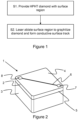
- Figure 1 is a flow diagram illustrating steps in forming a cutting element for a tool. The following numbering corresponds to that of Figure 1 .
- An HPHT PCD diamond cutting element is provided.
- the carbon in the PCD is in the form of diamond, and laser ablation converts some of the diamond carbon to the graphite form of carbon, thereby forming an electrically conductive track.
- the resistivity of graphite is around 1 ⁇ 10 -5 ohm ⁇ cm, making graphite a good conductor of electricity.
- the graphite track can therefore be used to carry data in the form of an electric signal.
- the cutting element 1 comprises a PCD layer 2 bonded to a support substrate 3.
- the support substrate 3 may be any suitable material, such as cemented tungsten carbide.
- the PCD layer 2 has a top (or rake) face 4, and a clearance face 5.
- the PCD contains cobalt in the interstices between ⁇ diamond grains.
- the cutting element 1 in one exemplary embodiment is therefore leached in HCl to remove cobalt close to the surface of the top face 4 and the clearance face 5, in order to increase the resistivity of the surface region and improve the electrical isolation of the electrically conductive track 6.
- a protective element such as an acid resistant tape (e.g. polyamide with a silicone adhesive) is used to protect the cemented tungsten carbide substrate 3 from the HCl.
- an acid resistant tape e.g. polyamide with a silicone adhesive
- Electrically conductive tracks were applied by using a Nd:YAG Q-switched high frequency laser.
- a power of between 10 and 12 ⁇ 10 6 Wcm -2 was used, at a frequency of 50 kHz, a pulse duration of 10 ⁇ s and a speed of 300 to 400 mms -1 .
- the electrically conductive track 6 was applied using the pulsed laser. Note that the track is shown as being applied on the top face 4 of the PCD layer 2. However, the track could also be applied on the clearance face 5 of the PCD layer 2, or could trace a path that includes both the top face 4 and the clearance face 5.
- the laser ablation energy was sufficient to form a trench in the surface of the PCD layer 2, and to convert diamond to graphite.
- the width of the ablated electrically conductive track 6 should be at least three times the average diamond grain size of the PCD to ensure that there are no breaks in the electrically conductive tracks that would otherwise affect the ability of the electrically conductive track to carry an electrical signal.
- a sensor 7 is provided towards the cutting tip of the cutting element 1.
- Exemplary sensors include wear sensors, vibration sensors, temperature sensors and so on.
- a data collection element 8 is also provided, which is an element that allows collected data to be moved to a storage device or a computer device for analysis of the data.
- the electrically conductive track 6 extends between the sensor 7 and the data collection element 8 so that data collected from the sensor can be transferred to the data collection element 8.
- PCD is a brittle material and wear or chipping can occur. For this reason, the working life of a cutting element is based on recommended times, at which point the cutting element is changed. However, a cutting element may, after this predetermined time, still have many potential hours of use. By using sensors to monitor conditions of the cutting element 1, the tool life can be more accurately monitored and the tool replaced shortly before an unacceptable amount of wear has occurred. This greatly increases the working life of cutting elements.
- the electrically conductive track can be used indirectly to measure temperature.
- Resistance Temperature Detectors are typically metallic and constructed from materials such as platinum, copper or nickel. These materials have a repeatable resistance versus temperature relationship. The resistance increases as the temperature increases. In contrast, it has been found that the graphite tracks display a resistance that decreases as the temperature increases. This behaviour is commonly observed in semiconductor materials.
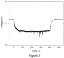
- FIG. 3 This effect is illustrated in Figure 3 ; a PCD cutting element was made with a graphitized track on the rake face. An electrical signal was applied to the graphitized track with a voltage just above 1.1 V. The cutting element was used to cut a work piece. The cutting operation lasted for 400 seconds. As can be seen from Figure 3 , the voltage quickly dropped once the cutting operation started. This is because the temperature of the cutting element increased. Resistance is directly proportional to voltage, and the resistance can be related to the resistivity of the electrically conductive graphite track using the length and the cross-section area of the electrically conductive graphite track.
- the resistivity of graphite as a function of temperature is known (for example, see Poco Graphite, Properties and Characteristics of Graphite, page 22 and 23, www.http://poco.com/Portals/0/Literature/Semiconductor/IND-109441-0115.pdf, accessed 6 February 2018).
- the resistivity of graphite does not change linearly with temperature, and so a calibration must be performed for an electrically conductive graphite track of known dimensions. After calibration, the voltage can be used to obtain an indication of the temperature of the electrically conductive graphite track, and so the electrically conductive graphite track itself becomes a temperature sensor.
- super-hard or ultra-hard material has Vickers hardness of at least 25 GPa.
- Synthetic and natural diamond, polycrystalline diamond (PCD), cubic boron nitride (CBN) and polycrystalline CBN (PCBN) material are examples of super-hard materials.
- Synthetic diamond which may also be called man-made diamond, is diamond material that has been manufactured.
- a PCD structure comprises or consists of PCD material.
- Other examples of super-hard materials include certain composite materials comprising diamond or CBN grains held together by a matrix comprising ceramic material, such as silicon carbide (SiC), or by cemented carbide material such as Co-bonded WC material.
- SiC-bonded diamond materials may comprise at least about 30 volume per cent diamond grains dispersed in a SiC matrix (which may contain a minor amount of Si in a form other than SiC).
- catalyst material for super-hard material is capable of promoting the sintering of polycrystalline material comprising grains of the super-hard material, at least at a pressure and temperature at which the super-hard material is thermodynamically stable.
- the catalyst material may be capable of promoting the direct inter-growth of grains of the super-hard material and or more generally the sintering of the grains of the super-hard material to form the polycrystalline material.
- the catalyst material may function as a binder material capable of forming a sintered matrix, on its own or in combination with other suitable material, within which the super-hard grains may be dispersed and not necessarily directly inter-bonded with each other.
- catalyst material for synthetic diamond is capable of promoting the growth of synthetic diamond grains and or the direct inter-growth of synthetic or natural diamond grains at a temperature and pressure at which synthetic or natural diamond is thermodynamically more stable than graphite.
- catalyst materials for diamond are Fe, Ni, Co and Mn, and certain alloys including these.
- Catalyst or binder material for PCBN material may comprising a Ti-containing compound, such as titanium carbide, titanium nitride, titanium carbonitride and or an Al-containing compound, such as aluminium nitride, and or compounds containing metal such as Co and or W, for example.
- polycrystalline diamond (PCD) material comprises a mass (an aggregation of a plurality) of diamond grains, a substantial portion of which are directly inter-bonded with each other and in which the content of diamond is at least about 80 volume per cent of the material. Interstices between the diamond grains may be at least partly filled with a binder material comprising a catalyst material for synthetic diamond, or they may be substantially empty. Bodies comprising PCD material may comprise at least a region from which catalyst material has been removed from the interstices, leaving interstitial voids between the diamond grains.
- a machine tool is a powered mechanical device, which may be used to manufacture components comprising materials such as metal, composite materials, wood or polymers by machining, which is the selective removal of material from a body, called a work-piece.
- a machine tool may comprise a cutter insert (or simply "insert”) comprising a cutter structure, and the insert may be indexable and or replaceable.
- Chips are the pieces of a body removed from the work surface of the body by a machine tool in use. Controlling chip formation and directing chip flow are important aspects of tools for high productivity machining and or high surface finish machining of advanced alloys of aluminium, titanium and Nickel.
- the geometry of chip-breaker features may be selected according to various machining factors, such as the work piece material, cutting speed, cutting operation and surface finish required.
Landscapes
- Engineering & Computer Science (AREA)
- Mechanical Engineering (AREA)
- Physics & Mathematics (AREA)
- Optics & Photonics (AREA)
- Plasma & Fusion (AREA)
- Cutting Tools, Boring Holders, And Turrets (AREA)
- Machine Tool Sensing Apparatuses (AREA)
- Earth Drilling (AREA)
Claims (15)
- Élément de coupe (1) pour un outil, l'élément de coupe (1) comportant :un corps en diamant polycristallin haute pression-haute température (2) comportant une zone de surface,une piste électriquement conductrice (6) formée au niveau de la zone de surface, dans lequel la piste électriquement conductrice (6) a une résistance électrique sensiblement inférieure à celle de la zone de surface, caractérisé en ce que la piste conductrice (6) comporte du graphite.
- Élément de coupe (1) selon la revendication 1, dans lequel la piste conductrice (6) a une largeur égale à au moins trois fois la taille de grain moyenne du diamant.
- Élément de coupe (1) selon l'une quelconque des revendications 1 ou 2, dans lequel au moins une extrémité de la piste conductrice (6) est reliée à un capteur (7) situé sur l'élément de coupe (1).
- Élément de coupe (1) selon l'une quelconque des revendications 1 à 3, dans lequel au moins une extrémité de la piste conductrice (6) est reliée à un élément de collecte de données (8).
- Élément de coupe (1) selon l'une quelconque des revendications 1 à 4, dans lequel le corps en diamant polycristallin haute pression-haute température (2) comporte une zone de surface sensiblement non conductrice.
- Élément de coupe (1) selon l'une quelconque des revendications 1 à 5, dans lequel la piste conductrice (6) est disposée sur une face quelconque parmi une face d'attaque (4) et une face de dégagement (5).
- Outil comportant l'élément de coupe (1) selon l'une quelconque des revendications 1 à 6.
- Outil selon la revendication 7, dans lequel l'outil est choisi parmi un élément quelconque parmi un foret, un outil de fraisage, un outil de tournage, un outil de forage, un outil d'alésage, une filière de tréfilage, un outil de pic de mineur, un outil de pic de fraisage routier et un trépan de fond de trou.
- Procédé de fabrication d'un élément de coupe (1) pour un outil, le procédé comportant les étapes consistant à :fournir un corps en diamant polycristallin haute pression-haute température (2) comportant une zone de surface,former une piste électriquement conductrice (6) au niveau de la zone de surface, dans lequel la piste électriquement conductrice (6) a une résistance électrique sensiblement inférieure à celle de la zone de surface, caractérisé en ce que la piste conductrice (6) comporte du graphite.
- Procédé selon la revendication 9, dans lequel la piste conductrice (6) est formée par ablation laser du diamant au niveau de la zone de surface.
- Procédé selon la revendication 10, dans lequel l'ablation au laser est réalisée en utilisant un laser Nd:YAG ayant une puissance comprise entre 8 et 14 × 106 Wcm-2.
- Procédé selon la revendication 10 ou 11, dans lequel l'ablation laser est pulsée à une fréquence comprise entre 20 et 100 kHz et une durée d'impulsion comprise entre 5 et 20 µs.
- Procédé selon l'une quelconque des revendications 10 à 12, dans lequel l'ablation laser est réalisée à une vitesse comprise entre 200 et 500 mms-1 le long de la zone de surface sensiblement non conductrice.
- Procédé selon l'une quelconque des revendications 9 à 13, comportant en outre le retrait du matériau liant conducteur situé au niveau de la zone de surface, le retrait étant réalisé par lixiviation.
- Procédé selon l'une quelconque des revendications 9 à 14, comportant en outre le retrait par lixiviation de matériau liant conducteur du corps en diamant polycristallin (2).
Applications Claiming Priority (2)
| Application Number | Priority Date | Filing Date | Title |
|---|---|---|---|
| GBGB1802112.1A GB201802112D0 (en) | 2018-02-09 | 2018-02-09 | Tool cutting element |
| PCT/EP2019/053173 WO2019155004A1 (fr) | 2018-02-09 | 2019-02-08 | Élément de coupe d'outil |
Publications (2)
| Publication Number | Publication Date |
|---|---|
| EP3749484A1 EP3749484A1 (fr) | 2020-12-16 |
| EP3749484B1 true EP3749484B1 (fr) | 2023-04-05 |
Family
ID=61731236
Family Applications (1)
| Application Number | Title | Priority Date | Filing Date |
|---|---|---|---|
| EP19703726.0A Active EP3749484B1 (fr) | 2018-02-09 | 2019-02-08 | Élément de coupe d'outil |
Country Status (7)
| Country | Link |
|---|---|
| US (1) | US11407038B2 (fr) |
| EP (1) | EP3749484B1 (fr) |
| JP (1) | JP6960059B2 (fr) |
| KR (1) | KR102187870B1 (fr) |
| CN (1) | CN111344109A (fr) |
| GB (2) | GB201802112D0 (fr) |
| WO (1) | WO2019155004A1 (fr) |
Families Citing this family (2)
| Publication number | Priority date | Publication date | Assignee | Title |
|---|---|---|---|---|
| CN114102259B (zh) * | 2021-11-23 | 2022-11-01 | 华中科技大学 | 一种金属基复合材料微细切削刀具与磨损监测方法 |
| US12269137B2 (en) | 2022-08-24 | 2025-04-08 | Kennametal Inc. | System and method for real-time monitoring and predicting wear of a cutting tool |
Citations (2)
| Publication number | Priority date | Publication date | Assignee | Title |
|---|---|---|---|---|
| JPH08197309A (ja) * | 1995-01-19 | 1996-08-06 | Fanuc Ltd | イオン注入したダイヤモンド切削工具 |
| US20090098814A1 (en) * | 2007-10-05 | 2009-04-16 | Chien-Min Sung | Polymeric Fiber CMP Pad and Associated Methods |
Family Cites Families (22)
| Publication number | Priority date | Publication date | Assignee | Title |
|---|---|---|---|---|
| NL8200430A (nl) * | 1982-02-04 | 1983-09-01 | Optische Ind De Oude Delft Nv | Werkwijze voor het vervaardigen van electrische contacten aan diamant met behulp van een laser, en diamant die volgens deze optische werkwijze is voorzien van contacten. |
| JP3359894B2 (ja) * | 1999-12-14 | 2002-12-24 | 京セラ株式会社 | 損耗センサ付きスローアウェイチップ |
| US6592303B2 (en) * | 2000-08-30 | 2003-07-15 | Kyocera Corporation | Throw-away tip |
| JP3840049B2 (ja) * | 2000-10-27 | 2006-11-01 | 京セラ株式会社 | スローアウェイチップ |
| JP3898427B2 (ja) * | 2000-08-30 | 2007-03-28 | 京セラ株式会社 | スローアウェイチップ及びその製造方法 |
| JP3924438B2 (ja) | 2001-03-29 | 2007-06-06 | 京セラ株式会社 | センサ付き切削工具およびその作製方法 |
| US7052215B2 (en) * | 2001-03-29 | 2006-05-30 | Kyocera Corporation | Cutting tool with sensor and production method therefor |
| DE10220755A1 (de) | 2001-05-08 | 2002-11-14 | Klaus Nordmann | Schneidwerkzeug |
| ES2816179T3 (es) * | 2008-02-06 | 2021-03-31 | Sumitomo Electric Industries | Diamante policristalino |
| JP5426319B2 (ja) * | 2009-10-26 | 2014-02-26 | 住友電気工業株式会社 | ダイヤモンド切削工具及びその製造方法 |
| US20120132468A1 (en) | 2010-11-30 | 2012-05-31 | Baker Hughes Incorporated | Cutter with diamond sensors for acquiring information relating to an earth-boring drilling tool |
| JP5914446B2 (ja) * | 2012-10-30 | 2016-05-11 | 株式会社アライドマテリアル | 切削工具およびそれを用いたワークの加工方法 |
| US9945185B2 (en) * | 2014-05-30 | 2018-04-17 | Baker Hughes Incorporated | Methods of forming polycrystalline diamond |
| JP2016074572A (ja) | 2014-10-08 | 2016-05-12 | 株式会社アライドマテリアル | 切削工具 |
| WO2016068231A1 (fr) * | 2014-10-29 | 2016-05-06 | 住友電気工業株式会社 | Corps en diamant composite et outil en diamant composite |
| US10364615B2 (en) * | 2014-11-12 | 2019-07-30 | Suzhou Superior Industrial Technology Co. Ltd. | Brazed polycrystalline diamond compact |
| DK3224607T3 (da) * | 2014-11-25 | 2024-11-11 | Element Six Tech Ltd | Elektrokemisk sensor omfattende bordoperet diamantelektrode |
| CN204424268U (zh) * | 2015-01-17 | 2015-06-24 | 王宏兴 | 一种半导体器件的三维电极结构 |
| RU2017133614A (ru) * | 2015-02-28 | 2019-03-28 | Элемент Сикс (Юк) Лимитид | Сверхтвердые конструкции и способы их получения |
| EP3106260B1 (fr) * | 2015-06-16 | 2018-11-28 | Sandvik Intellectual Property AB | Insert de coupe et outil pour couper, fraiser ou forer du métal |
| JP6036948B2 (ja) * | 2015-09-14 | 2016-11-30 | 住友電気工業株式会社 | 導電層付き単結晶ダイヤモンドおよびそれを用いた工具、ならびに導電層付き単結晶ダイヤモンドの製造方法 |
| CN106784044B (zh) * | 2016-12-26 | 2018-09-07 | 哈尔滨工业大学 | 一种三维结构金刚石紫外探测器及其制备方法 |
-
2018
- 2018-02-09 GB GBGB1802112.1A patent/GB201802112D0/en not_active Ceased
-
2019
- 2019-02-08 JP JP2020530501A patent/JP6960059B2/ja active Active
- 2019-02-08 WO PCT/EP2019/053173 patent/WO2019155004A1/fr not_active Ceased
- 2019-02-08 CN CN201980005675.6A patent/CN111344109A/zh active Pending
- 2019-02-08 US US16/754,305 patent/US11407038B2/en active Active
- 2019-02-08 GB GB1901776.3A patent/GB2572062B/en active Active
- 2019-02-08 EP EP19703726.0A patent/EP3749484B1/fr active Active
- 2019-02-08 KR KR1020207012246A patent/KR102187870B1/ko active Active
Patent Citations (2)
| Publication number | Priority date | Publication date | Assignee | Title |
|---|---|---|---|---|
| JPH08197309A (ja) * | 1995-01-19 | 1996-08-06 | Fanuc Ltd | イオン注入したダイヤモンド切削工具 |
| US20090098814A1 (en) * | 2007-10-05 | 2009-04-16 | Chien-Min Sung | Polymeric Fiber CMP Pad and Associated Methods |
Also Published As
| Publication number | Publication date |
|---|---|
| CN111344109A (zh) | 2020-06-26 |
| WO2019155004A1 (fr) | 2019-08-15 |
| GB201901776D0 (en) | 2019-03-27 |
| GB201802112D0 (en) | 2018-03-28 |
| JP2021505415A (ja) | 2021-02-18 |
| US11407038B2 (en) | 2022-08-09 |
| US20200238393A1 (en) | 2020-07-30 |
| JP6960059B2 (ja) | 2021-11-05 |
| KR102187870B1 (ko) | 2020-12-07 |
| GB2572062A (en) | 2019-09-18 |
| GB2572062B (en) | 2021-02-24 |
| EP3749484A1 (fr) | 2020-12-16 |
| KR20200051824A (ko) | 2020-05-13 |
Similar Documents
| Publication | Publication Date | Title |
|---|---|---|
| US6544308B2 (en) | High volume density polycrystalline diamond with working surfaces depleted of catalyzing material | |
| US8651204B2 (en) | Metal-free supported polycrystalline diamond and method to form | |
| US12044118B2 (en) | Sensor elements and assemblies, cutting tools comprising same and methods of using same | |
| EP1318969B1 (fr) | Diamant polycristallin a forte densite volumique comportant un materiau catalyseur a surfaces de travail appauvries | |
| US12065885B2 (en) | Cutting element and methods of making the same | |
| CA2865443A1 (fr) | Diamant polycristallin a surface pauvre en catalyseur | |
| CN107532458A (zh) | 超硬结构及其制造方法 | |
| US20230015853A1 (en) | Sensor elements for a cutting tool and methods of making and using same | |
| GB2577077A (en) | A tool module for real-time tool condition monitoring during precision machining | |
| EP3749484B1 (fr) | Élément de coupe d'outil | |
| US12188302B2 (en) | Sensor elements and assemblies, cutting tools comprising same and methods of using same | |
| GB2577078A (en) | A tool module for real-time tool condition monitoring during precision machining | |
| WO2019155005A1 (fr) | Élément de coupe d'outil | |
| US20190275642A1 (en) | Polycrystalline diamond construction and method for making same | |
| CN110267760A (zh) | 超硬构造及其制造方法 | |
| US12480396B2 (en) | Cutting elements for a cutting tool and methods of making and using same | |
| WO2020239800A1 (fr) | Produit de diamant polycristallin composte (pcd) et ses procédés de fabrication | |
| WO2023126450A1 (fr) | Éléments de coupe pour un outil de coupe et leurs procédés de fabrication et d'utilisation |
Legal Events
| Date | Code | Title | Description |
|---|---|---|---|
| STAA | Information on the status of an ep patent application or granted ep patent |
Free format text: STATUS: UNKNOWN |
|
| STAA | Information on the status of an ep patent application or granted ep patent |
Free format text: STATUS: THE INTERNATIONAL PUBLICATION HAS BEEN MADE |
|
| PUAI | Public reference made under article 153(3) epc to a published international application that has entered the european phase |
Free format text: ORIGINAL CODE: 0009012 |
|
| STAA | Information on the status of an ep patent application or granted ep patent |
Free format text: STATUS: REQUEST FOR EXAMINATION WAS MADE |
|
| 17P | Request for examination filed |
Effective date: 20200402 |
|
| AK | Designated contracting states |
Kind code of ref document: A1 Designated state(s): AL AT BE BG CH CY CZ DE DK EE ES FI FR GB GR HR HU IE IS IT LI LT LU LV MC MK MT NL NO PL PT RO RS SE SI SK SM TR |
|
| AX | Request for extension of the european patent |
Extension state: BA ME |
|
| DAV | Request for validation of the european patent (deleted) | ||
| DAX | Request for extension of the european patent (deleted) | ||
| REG | Reference to a national code |
Ref country code: DE Ref legal event code: R079 Ref document number: 602019027168 Country of ref document: DE Free format text: PREVIOUS MAIN CLASS: B23Q0017090000 Ipc: B23B0027140000 |
|
| STAA | Information on the status of an ep patent application or granted ep patent |
Free format text: STATUS: EXAMINATION IS IN PROGRESS |
|
| RIC1 | Information provided on ipc code assigned before grant |
Ipc: B23B 27/14 20060101AFI20210712BHEP Ipc: B23K 26/06 20140101ALI20210712BHEP Ipc: B23K 26/36 20140101ALI20210712BHEP |
|
| 17Q | First examination report despatched |
Effective date: 20210721 |
|
| GRAP | Despatch of communication of intention to grant a patent |
Free format text: ORIGINAL CODE: EPIDOSNIGR1 |
|
| STAA | Information on the status of an ep patent application or granted ep patent |
Free format text: STATUS: GRANT OF PATENT IS INTENDED |
|
| INTG | Intention to grant announced |
Effective date: 20221118 |
|
| GRAS | Grant fee paid |
Free format text: ORIGINAL CODE: EPIDOSNIGR3 |
|
| GRAA | (expected) grant |
Free format text: ORIGINAL CODE: 0009210 |
|
| STAA | Information on the status of an ep patent application or granted ep patent |
Free format text: STATUS: THE PATENT HAS BEEN GRANTED |
|
| AK | Designated contracting states |
Kind code of ref document: B1 Designated state(s): AL AT BE BG CH CY CZ DE DK EE ES FI FR GB GR HR HU IE IS IT LI LT LU LV MC MK MT NL NO PL PT RO RS SE SI SK SM TR |
|
| REG | Reference to a national code |
Ref country code: GB Ref legal event code: FG4D |
|
| REG | Reference to a national code |
Ref country code: CH Ref legal event code: EP |
|
| REG | Reference to a national code |
Ref country code: AT Ref legal event code: REF Ref document number: 1557870 Country of ref document: AT Kind code of ref document: T Effective date: 20230415 |
|
| REG | Reference to a national code |
Ref country code: DE Ref legal event code: R096 Ref document number: 602019027168 Country of ref document: DE |
|
| REG | Reference to a national code |
Ref country code: IE Ref legal event code: FG4D |
|
| P01 | Opt-out of the competence of the unified patent court (upc) registered |
Effective date: 20230524 |
|
| REG | Reference to a national code |
Ref country code: LT Ref legal event code: MG9D |
|
| REG | Reference to a national code |
Ref country code: NL Ref legal event code: MP Effective date: 20230405 |
|
| REG | Reference to a national code |
Ref country code: AT Ref legal event code: MK05 Ref document number: 1557870 Country of ref document: AT Kind code of ref document: T Effective date: 20230405 |
|
| PG25 | Lapsed in a contracting state [announced via postgrant information from national office to epo] |
Ref country code: NL Free format text: LAPSE BECAUSE OF FAILURE TO SUBMIT A TRANSLATION OF THE DESCRIPTION OR TO PAY THE FEE WITHIN THE PRESCRIBED TIME-LIMIT Effective date: 20230405 |
|
| PG25 | Lapsed in a contracting state [announced via postgrant information from national office to epo] |
Ref country code: SE Free format text: LAPSE BECAUSE OF FAILURE TO SUBMIT A TRANSLATION OF THE DESCRIPTION OR TO PAY THE FEE WITHIN THE PRESCRIBED TIME-LIMIT Effective date: 20230405 Ref country code: PT Free format text: LAPSE BECAUSE OF FAILURE TO SUBMIT A TRANSLATION OF THE DESCRIPTION OR TO PAY THE FEE WITHIN THE PRESCRIBED TIME-LIMIT Effective date: 20230807 Ref country code: NO Free format text: LAPSE BECAUSE OF FAILURE TO SUBMIT A TRANSLATION OF THE DESCRIPTION OR TO PAY THE FEE WITHIN THE PRESCRIBED TIME-LIMIT Effective date: 20230705 Ref country code: ES Free format text: LAPSE BECAUSE OF FAILURE TO SUBMIT A TRANSLATION OF THE DESCRIPTION OR TO PAY THE FEE WITHIN THE PRESCRIBED TIME-LIMIT Effective date: 20230405 Ref country code: AT Free format text: LAPSE BECAUSE OF FAILURE TO SUBMIT A TRANSLATION OF THE DESCRIPTION OR TO PAY THE FEE WITHIN THE PRESCRIBED TIME-LIMIT Effective date: 20230405 |
|
| PG25 | Lapsed in a contracting state [announced via postgrant information from national office to epo] |
Ref country code: RS Free format text: LAPSE BECAUSE OF FAILURE TO SUBMIT A TRANSLATION OF THE DESCRIPTION OR TO PAY THE FEE WITHIN THE PRESCRIBED TIME-LIMIT Effective date: 20230405 Ref country code: PL Free format text: LAPSE BECAUSE OF FAILURE TO SUBMIT A TRANSLATION OF THE DESCRIPTION OR TO PAY THE FEE WITHIN THE PRESCRIBED TIME-LIMIT Effective date: 20230405 Ref country code: LV Free format text: LAPSE BECAUSE OF FAILURE TO SUBMIT A TRANSLATION OF THE DESCRIPTION OR TO PAY THE FEE WITHIN THE PRESCRIBED TIME-LIMIT Effective date: 20230405 Ref country code: LT Free format text: LAPSE BECAUSE OF FAILURE TO SUBMIT A TRANSLATION OF THE DESCRIPTION OR TO PAY THE FEE WITHIN THE PRESCRIBED TIME-LIMIT Effective date: 20230405 Ref country code: IS Free format text: LAPSE BECAUSE OF FAILURE TO SUBMIT A TRANSLATION OF THE DESCRIPTION OR TO PAY THE FEE WITHIN THE PRESCRIBED TIME-LIMIT Effective date: 20230805 Ref country code: HR Free format text: LAPSE BECAUSE OF FAILURE TO SUBMIT A TRANSLATION OF THE DESCRIPTION OR TO PAY THE FEE WITHIN THE PRESCRIBED TIME-LIMIT Effective date: 20230405 Ref country code: GR Free format text: LAPSE BECAUSE OF FAILURE TO SUBMIT A TRANSLATION OF THE DESCRIPTION OR TO PAY THE FEE WITHIN THE PRESCRIBED TIME-LIMIT Effective date: 20230706 Ref country code: AL Free format text: LAPSE BECAUSE OF FAILURE TO SUBMIT A TRANSLATION OF THE DESCRIPTION OR TO PAY THE FEE WITHIN THE PRESCRIBED TIME-LIMIT Effective date: 20230405 |
|
| PG25 | Lapsed in a contracting state [announced via postgrant information from national office to epo] |
Ref country code: FI Free format text: LAPSE BECAUSE OF FAILURE TO SUBMIT A TRANSLATION OF THE DESCRIPTION OR TO PAY THE FEE WITHIN THE PRESCRIBED TIME-LIMIT Effective date: 20230405 |
|
| REG | Reference to a national code |
Ref country code: DE Ref legal event code: R097 Ref document number: 602019027168 Country of ref document: DE |
|
| PG25 | Lapsed in a contracting state [announced via postgrant information from national office to epo] |
Ref country code: SK Free format text: LAPSE BECAUSE OF FAILURE TO SUBMIT A TRANSLATION OF THE DESCRIPTION OR TO PAY THE FEE WITHIN THE PRESCRIBED TIME-LIMIT Effective date: 20230405 |
|
| PG25 | Lapsed in a contracting state [announced via postgrant information from national office to epo] |
Ref country code: SM Free format text: LAPSE BECAUSE OF FAILURE TO SUBMIT A TRANSLATION OF THE DESCRIPTION OR TO PAY THE FEE WITHIN THE PRESCRIBED TIME-LIMIT Effective date: 20230405 Ref country code: SK Free format text: LAPSE BECAUSE OF FAILURE TO SUBMIT A TRANSLATION OF THE DESCRIPTION OR TO PAY THE FEE WITHIN THE PRESCRIBED TIME-LIMIT Effective date: 20230405 Ref country code: RO Free format text: LAPSE BECAUSE OF FAILURE TO SUBMIT A TRANSLATION OF THE DESCRIPTION OR TO PAY THE FEE WITHIN THE PRESCRIBED TIME-LIMIT Effective date: 20230405 Ref country code: EE Free format text: LAPSE BECAUSE OF FAILURE TO SUBMIT A TRANSLATION OF THE DESCRIPTION OR TO PAY THE FEE WITHIN THE PRESCRIBED TIME-LIMIT Effective date: 20230405 Ref country code: DK Free format text: LAPSE BECAUSE OF FAILURE TO SUBMIT A TRANSLATION OF THE DESCRIPTION OR TO PAY THE FEE WITHIN THE PRESCRIBED TIME-LIMIT Effective date: 20230405 Ref country code: CZ Free format text: LAPSE BECAUSE OF FAILURE TO SUBMIT A TRANSLATION OF THE DESCRIPTION OR TO PAY THE FEE WITHIN THE PRESCRIBED TIME-LIMIT Effective date: 20230405 |
|
| PLBE | No opposition filed within time limit |
Free format text: ORIGINAL CODE: 0009261 |
|
| STAA | Information on the status of an ep patent application or granted ep patent |
Free format text: STATUS: NO OPPOSITION FILED WITHIN TIME LIMIT |
|
| 26N | No opposition filed |
Effective date: 20240108 |
|
| PG25 | Lapsed in a contracting state [announced via postgrant information from national office to epo] |
Ref country code: SI Free format text: LAPSE BECAUSE OF FAILURE TO SUBMIT A TRANSLATION OF THE DESCRIPTION OR TO PAY THE FEE WITHIN THE PRESCRIBED TIME-LIMIT Effective date: 20230405 |
|
| PG25 | Lapsed in a contracting state [announced via postgrant information from national office to epo] |
Ref country code: SI Free format text: LAPSE BECAUSE OF FAILURE TO SUBMIT A TRANSLATION OF THE DESCRIPTION OR TO PAY THE FEE WITHIN THE PRESCRIBED TIME-LIMIT Effective date: 20230405 Ref country code: IT Free format text: LAPSE BECAUSE OF FAILURE TO SUBMIT A TRANSLATION OF THE DESCRIPTION OR TO PAY THE FEE WITHIN THE PRESCRIBED TIME-LIMIT Effective date: 20230405 |
|
| PG25 | Lapsed in a contracting state [announced via postgrant information from national office to epo] |
Ref country code: MC Free format text: LAPSE BECAUSE OF FAILURE TO SUBMIT A TRANSLATION OF THE DESCRIPTION OR TO PAY THE FEE WITHIN THE PRESCRIBED TIME-LIMIT Effective date: 20230405 |
|
| REG | Reference to a national code |
Ref country code: CH Ref legal event code: PL |
|
| PG25 | Lapsed in a contracting state [announced via postgrant information from national office to epo] |
Ref country code: LU Free format text: LAPSE BECAUSE OF NON-PAYMENT OF DUE FEES Effective date: 20240208 |
|
| PG25 | Lapsed in a contracting state [announced via postgrant information from national office to epo] |
Ref country code: CH Free format text: LAPSE BECAUSE OF NON-PAYMENT OF DUE FEES Effective date: 20240229 |
|
| PG25 | Lapsed in a contracting state [announced via postgrant information from national office to epo] |
Ref country code: LU Free format text: LAPSE BECAUSE OF NON-PAYMENT OF DUE FEES Effective date: 20240208 Ref country code: CH Free format text: LAPSE BECAUSE OF NON-PAYMENT OF DUE FEES Effective date: 20240229 |
|
| PG25 | Lapsed in a contracting state [announced via postgrant information from national office to epo] |
Ref country code: BG Free format text: LAPSE BECAUSE OF FAILURE TO SUBMIT A TRANSLATION OF THE DESCRIPTION OR TO PAY THE FEE WITHIN THE PRESCRIBED TIME-LIMIT Effective date: 20230405 |
|
| PG25 | Lapsed in a contracting state [announced via postgrant information from national office to epo] |
Ref country code: BG Free format text: LAPSE BECAUSE OF FAILURE TO SUBMIT A TRANSLATION OF THE DESCRIPTION OR TO PAY THE FEE WITHIN THE PRESCRIBED TIME-LIMIT Effective date: 20230405 |
|
| REG | Reference to a national code |
Ref country code: BE Ref legal event code: MM Effective date: 20240229 |
|
| PG25 | Lapsed in a contracting state [announced via postgrant information from national office to epo] |
Ref country code: BE Free format text: LAPSE BECAUSE OF NON-PAYMENT OF DUE FEES Effective date: 20240229 |
|
| PG25 | Lapsed in a contracting state [announced via postgrant information from national office to epo] |
Ref country code: FR Free format text: LAPSE BECAUSE OF NON-PAYMENT OF DUE FEES Effective date: 20240229 |
|
| PG25 | Lapsed in a contracting state [announced via postgrant information from national office to epo] |
Ref country code: IE Free format text: LAPSE BECAUSE OF NON-PAYMENT OF DUE FEES Effective date: 20240208 |
|
| PG25 | Lapsed in a contracting state [announced via postgrant information from national office to epo] |
Ref country code: IE Free format text: LAPSE BECAUSE OF NON-PAYMENT OF DUE FEES Effective date: 20240208 Ref country code: FR Free format text: LAPSE BECAUSE OF NON-PAYMENT OF DUE FEES Effective date: 20240229 Ref country code: BE Free format text: LAPSE BECAUSE OF NON-PAYMENT OF DUE FEES Effective date: 20240229 |
|
| PG25 | Lapsed in a contracting state [announced via postgrant information from national office to epo] |
Ref country code: CY Free format text: LAPSE BECAUSE OF FAILURE TO SUBMIT A TRANSLATION OF THE DESCRIPTION OR TO PAY THE FEE WITHIN THE PRESCRIBED TIME-LIMIT; INVALID AB INITIO Effective date: 20190208 |
|
| PG25 | Lapsed in a contracting state [announced via postgrant information from national office to epo] |
Ref country code: HU Free format text: LAPSE BECAUSE OF FAILURE TO SUBMIT A TRANSLATION OF THE DESCRIPTION OR TO PAY THE FEE WITHIN THE PRESCRIBED TIME-LIMIT; INVALID AB INITIO Effective date: 20190208 |
|
| PG25 | Lapsed in a contracting state [announced via postgrant information from national office to epo] |
Ref country code: TR Free format text: LAPSE BECAUSE OF FAILURE TO SUBMIT A TRANSLATION OF THE DESCRIPTION OR TO PAY THE FEE WITHIN THE PRESCRIBED TIME-LIMIT Effective date: 20230405 |
|
| PGFP | Annual fee paid to national office [announced via postgrant information from national office to epo] |
Ref country code: GB Payment date: 20260227 Year of fee payment: 8 |
|
| PGFP | Annual fee paid to national office [announced via postgrant information from national office to epo] |
Ref country code: DE Payment date: 20260227 Year of fee payment: 8 |