EP3751602A1 - Substrat métallique isolé pour un groupe électronique de puissance - Google Patents
Substrat métallique isolé pour un groupe électronique de puissance Download PDFInfo
- Publication number
- EP3751602A1 EP3751602A1 EP19179373.6A EP19179373A EP3751602A1 EP 3751602 A1 EP3751602 A1 EP 3751602A1 EP 19179373 A EP19179373 A EP 19179373A EP 3751602 A1 EP3751602 A1 EP 3751602A1
- Authority
- EP
- European Patent Office
- Prior art keywords
- thermal
- elements
- metal substrate
- insulated metal
- ims
- Prior art date
- Legal status (The legal status is an assumption and is not a legal conclusion. Google has not performed a legal analysis and makes no representation as to the accuracy of the status listed.)
- Withdrawn
Links
Images

Classifications
-
- H—ELECTRICITY
- H10—SEMICONDUCTOR DEVICES; ELECTRIC SOLID-STATE DEVICES NOT OTHERWISE PROVIDED FOR
- H10W—GENERIC PACKAGES, INTERCONNECTIONS, CONNECTORS OR OTHER CONSTRUCTIONAL DETAILS OF DEVICES COVERED BY CLASS H10
- H10W40/00—Arrangements for thermal protection or thermal control
- H10W40/20—Arrangements for cooling
- H10W40/25—Arrangements for cooling characterised by their materials
- H10W40/255—Arrangements for cooling characterised by their materials having a laminate or multilayered structure, e.g. direct bond copper [DBC] ceramic substrates
-
- H—ELECTRICITY
- H10—SEMICONDUCTOR DEVICES; ELECTRIC SOLID-STATE DEVICES NOT OTHERWISE PROVIDED FOR
- H10W—GENERIC PACKAGES, INTERCONNECTIONS, CONNECTORS OR OTHER CONSTRUCTIONAL DETAILS OF DEVICES COVERED BY CLASS H10
- H10W40/00—Arrangements for thermal protection or thermal control
- H10W40/20—Arrangements for cooling
- H10W40/22—Arrangements for cooling characterised by their shape, e.g. having conical or cylindrical projections
- H10W40/226—Arrangements for cooling characterised by their shape, e.g. having conical or cylindrical projections characterised by projecting parts, e.g. fins to increase surface area
-
- H—ELECTRICITY
- H10—SEMICONDUCTOR DEVICES; ELECTRIC SOLID-STATE DEVICES NOT OTHERWISE PROVIDED FOR
- H10W—GENERIC PACKAGES, INTERCONNECTIONS, CONNECTORS OR OTHER CONSTRUCTIONAL DETAILS OF DEVICES COVERED BY CLASS H10
- H10W72/00—Interconnections or connectors in packages
- H10W72/50—Bond wires
- H10W72/531—Shapes of wire connectors
- H10W72/5363—Shapes of wire connectors the connected ends being wedge-shaped
-
- H—ELECTRICITY
- H10—SEMICONDUCTOR DEVICES; ELECTRIC SOLID-STATE DEVICES NOT OTHERWISE PROVIDED FOR
- H10W—GENERIC PACKAGES, INTERCONNECTIONS, CONNECTORS OR OTHER CONSTRUCTIONAL DETAILS OF DEVICES COVERED BY CLASS H10
- H10W72/00—Interconnections or connectors in packages
- H10W72/90—Bond pads, in general
- H10W72/921—Structures or relative sizes of bond pads
- H10W72/926—Multiple bond pads having different sizes
-
- H—ELECTRICITY
- H10—SEMICONDUCTOR DEVICES; ELECTRIC SOLID-STATE DEVICES NOT OTHERWISE PROVIDED FOR
- H10W—GENERIC PACKAGES, INTERCONNECTIONS, CONNECTORS OR OTHER CONSTRUCTIONAL DETAILS OF DEVICES COVERED BY CLASS H10
- H10W90/00—Package configurations
- H10W90/701—Package configurations characterised by the relative positions of pads or connectors relative to package parts
- H10W90/751—Package configurations characterised by the relative positions of pads or connectors relative to package parts of bond wires
- H10W90/754—Package configurations characterised by the relative positions of pads or connectors relative to package parts of bond wires between a chip and a stacked insulating package substrate, interposer or RDL
Definitions
- the invention relates to an insulated metal substrate with a thermal-mechanical interface for a power electronic assembly.
- the invention further relates to a power electronic assembly, a power electronic module, a system and an element.
- Conventional power electronic modules can have several thermal and mechanical interfaces in the primary cooling path.
- one or more ceramic substrates with metallization on both sides are typically used. This can be the case, for example, when several electrical potentials are required on the wiring carrier and electrical insulation in the direction of the primary cooling path.
- the ceramic core of the wiring carrier serves as electrical insulation, mechanical carrier and a thermally highly conductive path.
- the connection to the heat sink, which realizes the heat flow to the environment (air or liquid), takes place either via additional base plates to improve the heat spread and mechanical stability or directly by mounting the ceramic wiring supports on the respective heat sinks.
- thermal interface material for short, in English: thermal interface material
- TIM thermal interface material
- repairability As organic and often pasty materials, these materials are subject to various degradation effects in the field. For example, the influence of temperature fluctuations causes displacement effects of the material from the gaps, which leads to local defects in the TIM layer (so-called pump-out effects). Furthermore, these materials are subject to various undesirable aging phenomena.
- the invention is based on the object of enabling power electronic assemblies with insulated metal substrates without thermal interface materials.
- the object is achieved by an insulated metal substrate for a power electronic assembly that generates waste heat.
- the isolated metal substrate has a dielectric layer, a metallic base and at least one thermal-mechanical interface.
- a control plane made of an electrically conductive material, e.g. B. copper, be applied.
- the control plane can be applied over a large area in order to be structured in a later process step or it can already be designed as a structured or pre-structured control plane and thereby already form first conductor tracks.
- the thermal-mechanical interface also referred to below as the interface, is designed to dissipate the waste heat from the base and to make thermal contact with one or more elements.
- the thermal contact is ensured, among other things, by the mechanical design of the interface, such as depressions.
- the elements can be individual heat sink ribs, heat sink rods or other more complex (cooling) elements that match the mechanical design of the interface, for example according to a socket-plug and / or tongue-and-groove principle.
- the elements serve to improve the heat dissipation from the interface and thus from the base.
- the combination of several elements can improve the cooling capacity of the interface.
- lamellas, pins etc. can be provided as elements.
- the interface is designed accordingly so that the elements have a particularly good thermal connection to the interface.
- surface coatings can be provided in the interface and / or on the elements.
- surface coatings are particularly suitable, the intermetallic phases form, for example tinned elements or a tinned interface.
- the particular advantage of the present invention lies in being able to use the advantages of a heat sink integrated into the metal substrate without having to carry its considerable thermal mass with it in the entire manufacturing process.
- the manufacturing process can relate to the metal substrate itself or to an electronic power module with the metal substrate.
- the handling of the isolated metal substrates according to the present invention does not differ from the handling of conventional metal substrates, so that no or only insignificant changes to the handling devices in the manufacturing process are necessary.
- the thermal-mechanical interface is designed at least for partial mechanical fastening of the elements. This can be done through the geometric design of the thermal interface.
- the introduction of the elements into the interface can be designed as a fit and can be introduced into the interface by thermal shrinking on / in or by utilizing thermal expansion effects.
- the thermal-mechanical interface has one or more cutouts.
- the recesses are designed in such a way that they are used for mechanical fastening and / or for thermal contacting of the elements.
- the elements can be at least partially accommodated in the recesses; this can be implemented, for example, by pressing in, screwing in, so-called snap-in elements. Also screw connections, through z. B. by a thread, which serves as a recess, can be provided.
- the recesses are designed so that one or more of the elements can be inserted laterally. Lateral is here than sideways with regard to the plane on which the power electronic components are mounted. This is particularly advantageous since it avoids excessive mechanical stress on the sensitive electronic power components mounted on the insulated metal substrate. This is the case because the forces during the assembly of the elements only act in a lateral direction on the insulated metal substrate and thus only indirectly and laterally on the components, which means that the load is considerably lower and the reject rate (e.g. broken / cracked power semiconductors) is reduced can be. Compressive loads on any bonding wires that may be present and their potting materials can thus be completely avoided, so that undesired kinking of the bonding wires can be eliminated.
- the interface is designed in such a way that the forces of the element assembly act only indirectly on the components and thus only a slight interaction with the components that have already been assembled occurs during the assembly of the elements.
- the thermal-mechanical interface is designed for a form-fitting and / or force-fitting mechanical connection with the elements.
- the mechanical connection can only be configured in sections with respect to the element. This means that the element can only partially be mechanically connected to the interface in a form-fitting and / or force-fitting manner.
- the positive and / or non-positive mechanical connection enables the interface to improve the mechanical hold for the elements.
- the isolated metal substrate can hold the elements solely through the interface and its mechanical holding capabilities.
- the interface can support the insulated metal substrate itself, e.g. by elements that are provided on a frame / housing.
- the isolated metal substrate can be used flexibly thanks to the interface.
- the thermal-mechanical interface is at least partially cohesive thermal contacting of the elements formed.
- cohesive thermal contacts include the sintering of heat sinks or heat sink elements, in particular pressure-less sintering.
- a sufficient base thickness is advantageous in order to avoid thermal or thermomechanical damage to the dielectric layer.
- the interface is used as a coupling surface to a liquid metal with good thermal conductivity.
- the liquid metal is suitably surrounded by a material and / or a suitable geometry of the interface that ensures the mechanical coupling to the interface.
- the interface can be topographically shaped, which increases the surface area of the interface, e.g. Corrugated pattern.
- the elements can still be soldered, e.g. by means of diffusion soldering.
- the thermal-mechanical interface and the base are designed in one piece. This can be achieved through primary forming manufacturing processes. Furthermore, this can be realized by additive manufacturing processes or by subtractive (eg machining) manufacturing processes, each with or without a semi-finished product.
- the one-piece embodiment has the particular advantage that the thermal-mechanical interface is mechanically significantly more stable, and so are the thermal contact resistances can be reduced to the thermal-mechanical interface.
- the thermal-mechanical interface is designed for thermal connection of elements without thermal interface material.
- the thermal-mechanical interface is designed in such a way that direct contact can be established between the interface and the elements.
- the thermal-mechanical interface has grooves and / or tongues for a tongue and groove connection with the elements. Due to their larger surface and thus better heat transfer and at the same time mechanical holding function, these are particularly well suited for the thermal-mechanical interface. The elements can then accordingly form the counterparts for the tongue and groove connections.
- the object is also achieved by a power electronics assembly that has an insulated metal substrate according to the above embodiments and one or more power electronics components.
- the power electronic components can be arranged on a control plane and contacted by means of bonding wires. Bond wire-free and / or planar contacting technologies are also compatible.
- the assembly of the power electronic components can advantageously be carried out before the thermal contacting of the elements, since the contacting of the elements acts on the assembly with only low thermal and / or mechanical loads.
- the thermal-mechanical interface of the insulated metal substrate is arranged such that the thermal resistance between the power electronic components and the interface is minimal, that is to say that a particularly good heat exchange between the power electronic component and the thermal interface or the elements takes place.
- This can be implemented, for example, in that the thermal-mechanical interface is arranged below the assembly areas and / or has recesses for the elements below the assembly areas of the power electronic components.
- particularly powerful elements for example with extended liquid cooling and / or a large surface, can be provided below the power electronic components, which allow particularly good heat dissipation.
- the object is also achieved by a power electronics module that has at least one power electronics assembly according to one of the above embodiments and one or more elements.
- a power electronics system that has one or more power electronics assemblies and a carrier.
- the carrier has one or more elements and is designed for thermal contacting of the one or more power electronic assemblies.
- the thermal contact with the power electronic assemblies is established via the thermal interfaces of the insulated metal substrates.
- the elements can be combined to form system interfaces on the carrier side which, as a counterpart to the thermal interface of the insulated metal substrate, produce a mechanical holding function and / or a thermal contact function between the carrier and the assembly. It is particularly advantageous if the system has several power electronic assemblies, so several assemblies can be arranged on a single carrier with several elements.
- the elements are designed in such a way that they are used at least for partially mechanically fastening the assembly.
- the object is also achieved by an element for use with an insulated metal substrate.
- the element is designed such that it can be contacted both thermally and mechanically with the thermal interface.
- the element is provided with a surface coating which improves the heat conduction between the thermal interface of the insulated metal substrate and the element or reduces the thermal contact resistance.
- the elements are preferably made of materials with good thermal conductivity.
- FIG 1 shows an insulated metal substrate IMS as part of a power electronics assembly 100.
- the power electronics assembly 100 also has a control plane 140, which in this case has already been structured in order to produce electrical connections.
- the control plane 140 can be designed as a structured multipotential control plane and can be produced, for example, with a PCB method, by exposing a photosensitive layer, developing and etching will.
- the control level can be laminated flat, for example with copper, manufactured with the insulated metal substrate and structured in the further production process.
- Power electronic components 150 which in this case have been electrically contacted by means of bonding wires 155, are attached to the control level 140.
- Alternative chip contact options such as flip chips, wafer level packages or ball grid arrays or the like, are also possible.
- the power electronic components can be, for example, IGBTs, MOSFETs, diodes or other power semiconductors.
- the insulated metal substrate IMS has a dielectric layer 10 which separates the conductive plane 140 from a metallic base 20 of the insulated metal substrate IMS.
- the dielectric layer 10 is designed in such a way that it has good thermal conductivity, that is to say that it can pass the waste heat from the power electronic components 150 to the metallic base 20 of the insulated metal substrate IMS.
- the dielectric layer 10 has a thickness d10 of preferably 20 to 500 ⁇ m, in particular 50 to 200 ⁇ m, and can, for. B. be designed as a ceramic-filled dielectric made of epoxy resin.
- the metallic base 20 serves as a heat spreader and distributes the absorbed heat evenly.
- the metallic base 20 has a thickness d20 of preferably 0.6 to 5 mm, in particular 1.5 to 4 mm.
- the insulated metal substrate has a thermal-mechanical interface 30, which in this case has five cutouts 31,..., 35.
- the interface 30 has a thickness d30 of preferably 0.3 to 2 mm.
- the recesses 31, ..., 35 are preferably designed so that they can accommodate one or more elements (not shown), the elements serving, for example, as a heat sink and / or as a heat conduction element for heat conduction to a heat sink such as a water cooling system.
- the recess 31 has a width b31 of preferably 0.5 mm to 2 mm and is representative of all the recesses 31,..., 35. If undercuts are provided in the recesses 31, ..., 35, the recesses 31, ..., 35 can become somewhat wider with increasing depth.
- the Interface 30 is preferably designed so that the elements that can be mounted in interface 30 are mechanically fixed. This can be achieved by designing the recesses 31,..., 35.
- FIG 2 shows a power electronics assembly 100 which forms a power electronics module 400 with elements 301,..., 304.
- the assembly 100 is similar to that in FIG FIG 1 shown, wherein the thermal-mechanical interface 30 has different configurations.
- the elements 301 to 304 are here already mechanically fastened in the interface 30; e.g. through assembly.
- the element 301 can have a spring-like element in order to achieve a hold in the interface 30.
- the element 301 can be a single heat sink pin or a heat sink rib.
- An element 302 has a pin-shaped tip and can also be designed as a pin or rib.
- the elements 301, 302 can be introduced into the interface 30 using thermal methods.
- the elements 301, 302 can be cooled and the power electronic assembly can be heated up somewhat. As a result of the temperature difference, the elements 301, 302 can be introduced into the interface 30; mechanical hold is created when the temperature is equalized.
- An element 303 has a so-called snap-in connection and can be plugged mechanically and is fixed by the geometry. The snap-in connection can be designed in such a way that, after being plugged in once, the element 303 is no longer releasably connected.
- An element 304 shows a larger heat sink which, similar to the elements 301 and 302, has a spring-like element and a pin-shaped tip. The element 304 or the heat sink extends over two recesses 34, 35, other forms of contact and other numbers of recesses being possible depending on the size and type of the heat sink.
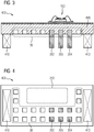
- FIG 3 shows a modularly equipped power electronic module 400, which in addition to the electronic assembly 100 already is equipped with elements 302, 303 and 304.
- the module 400 has only one power electronic component 150.
- the module 400 has edge elements 410 which can serve, for example, for mechanical stabilization and / or for attaching the insulated metal substrate IMS with its power electronic components 150 in a higher-level arrangement. This could include a housing or another circuit, for example.
- the edge elements can be part of a frame 50 (not shown) or be connected to it. In addition to their mechanical holding function, the edge elements 410 can also have a heat conducting function.
- FIG 4 shows the modularly equipped power electronic module 400 FIG 3 in a view from below.
- the elements 302, 303 and 304 are pin-shaped and are arranged in such a way that the first and second rows are fully occupied with elements 302, ..., 304, but at least in the middle there are no elements in the third and fourth rows are provided.
- This modular occupancy increases the flexibility of the interface 30.
- a surface 310 is free of the interface 30.
- standardized metal substrates could be designed, where power electronic components 150 are arranged above the interface 30 and accordingly no components generating waste heat are arranged above the surface 310.
- the surface 310 can serve for the arrangement of further components, such as processors, etc.
- Not fitting parts of the interface with elements 301, ..., 304 is not only efficient and cost-saving, it also saves installation space if simply no elements 302, ..., 304 are arranged where only little waste heat is generated. Little waste heat is produced if no power electronic components 150 are provided at this point or components that produce less waste heat.
- the modular equipping is given in all shown embodiments of the isolated metal substrate IMS.
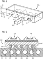
- FIG 5 shows an isolated metal substrate IMS in a three-dimensional view.
- the insulated metal substrate IMS is designed with cutouts 31, 32, 33 in the form of grooves, which in this case are designed for laterally receiving elements, for example as indicated the element 303, in the lateral direction LAT.
- This has the particular advantage of low mechanical loads on the insulated metal substrate IMS and the power electronics assembly 100 or their power electronics components 150 (not shown). The loads are in particular lower in comparison with methods which exert forces in a direction perpendicular to the plane of the insulated metal substrate IMS.
- FIG 6 shows an insulated metal substrate IMS as part of a power electronics assembly 100, which in turn is part of a power electronics system 500.
- the power electronics system 500 also has a carrier 50 with cooling channels 51 integrated therein.
- the power electronic system 500 has a system interface 550.
- the system interface 550 has elements 301 to 305, shown here only schematically.
- the elements 301 to 305 of the system interface 550 are used for thermal contacting of the insulated metal substrate and thus in a particularly advantageous manner dissipate the heat from the insulated metal substrate IMS or the power electronic assembly 100.
- the system interface 550 can have elements 301 to 305 which are designed in accordance with any shown embodiments or combinations thereof.
- the system interface 550 can furthermore also be designed in such a way that it offers mechanical support for the power electronic assembly 100.
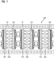
- FIG 7 shows a further particularly advantageous embodiment of a power electronic system 500 with three double-sided system interfaces 550.
- the system interfaces 550 are each designed for thermal and / or mechanical contacting of power electronic assemblies 100.
- the system interfaces 550 are connected to a carrier 50, which in turn has cooling channels 51.
- the system interfaces 550 also have their own cooling channels.
- the presence of cooling channels 51 is optional and can also be replaced by known alternative cooling options.
- the embodiment shown makes it possible to arrange power electronic assemblies 100 in a particularly high density and to cool them efficiently thanks to the cooling infrastructure comprising the system interfaces 550 and the carriers 50.
- the invention relates to an insulated metal substrate IMS for a power electronics assembly 100.
- the invention also relates to a power electronics assembly 100, a power electronics module 400, a system 500 and an element 301,..., 305.
- an insulated metal substrate IMS is proposed for a power electronic assembly 100 that generates waste heat.
- the insulated metal substrate IMS has a dielectric layer 10, a metallic base 20 and at least one thermal-mechanical interface 30.
- the thermal-mechanical interface 30 is designed to dissipate the waste heat from the base 20 and to make thermal contact with one or more elements 301,..., 305.
Landscapes
- Cooling Or The Like Of Semiconductors Or Solid State Devices (AREA)
Priority Applications (1)
| Application Number | Priority Date | Filing Date | Title |
|---|---|---|---|
| EP19179373.6A EP3751602A1 (fr) | 2019-06-11 | 2019-06-11 | Substrat métallique isolé pour un groupe électronique de puissance |
Applications Claiming Priority (1)
| Application Number | Priority Date | Filing Date | Title |
|---|---|---|---|
| EP19179373.6A EP3751602A1 (fr) | 2019-06-11 | 2019-06-11 | Substrat métallique isolé pour un groupe électronique de puissance |
Publications (1)
| Publication Number | Publication Date |
|---|---|
| EP3751602A1 true EP3751602A1 (fr) | 2020-12-16 |
Family
ID=66912548
Family Applications (1)
| Application Number | Title | Priority Date | Filing Date |
|---|---|---|---|
| EP19179373.6A Withdrawn EP3751602A1 (fr) | 2019-06-11 | 2019-06-11 | Substrat métallique isolé pour un groupe électronique de puissance |
Country Status (1)
| Country | Link |
|---|---|
| EP (1) | EP3751602A1 (fr) |
Cited By (3)
| Publication number | Priority date | Publication date | Assignee | Title |
|---|---|---|---|---|
| EP4084058A1 (fr) * | 2021-04-27 | 2022-11-02 | Siemens Aktiengesellschaft | Module électronique pourvu de porte-circuit, de puce à semi-conducteur et de dissipateur thermique |
| CN116435264A (zh) * | 2023-06-12 | 2023-07-14 | 江苏宏微科技股份有限公司 | 功率半导体模块 |
| US20240107718A1 (en) * | 2022-09-28 | 2024-03-28 | Delphi Technologies Ip Limited | Systems and methods for an interlocking feature on a power module |
Citations (5)
| Publication number | Priority date | Publication date | Assignee | Title |
|---|---|---|---|---|
| JPH08107166A (ja) * | 1994-10-06 | 1996-04-23 | Mitsubishi Materials Corp | 放熱用フィン |
| JP2011091088A (ja) * | 2009-10-20 | 2011-05-06 | Yaskawa Electric Corp | 発熱体の放熱構造、および該放熱構造を用いた半導体装置 |
| JP2011159743A (ja) * | 2010-01-29 | 2011-08-18 | Denso Corp | 半導体パッケージの防水構造 |
| JP2013165122A (ja) * | 2012-02-09 | 2013-08-22 | Mitsubishi Electric Corp | 半導体装置およびその製造方法 |
| JP2014179394A (ja) * | 2013-03-14 | 2014-09-25 | Mitsubishi Electric Corp | 半導体装置 |
-
2019
- 2019-06-11 EP EP19179373.6A patent/EP3751602A1/fr not_active Withdrawn
Patent Citations (5)
| Publication number | Priority date | Publication date | Assignee | Title |
|---|---|---|---|---|
| JPH08107166A (ja) * | 1994-10-06 | 1996-04-23 | Mitsubishi Materials Corp | 放熱用フィン |
| JP2011091088A (ja) * | 2009-10-20 | 2011-05-06 | Yaskawa Electric Corp | 発熱体の放熱構造、および該放熱構造を用いた半導体装置 |
| JP2011159743A (ja) * | 2010-01-29 | 2011-08-18 | Denso Corp | 半導体パッケージの防水構造 |
| JP2013165122A (ja) * | 2012-02-09 | 2013-08-22 | Mitsubishi Electric Corp | 半導体装置およびその製造方法 |
| JP2014179394A (ja) * | 2013-03-14 | 2014-09-25 | Mitsubishi Electric Corp | 半導体装置 |
Cited By (6)
| Publication number | Priority date | Publication date | Assignee | Title |
|---|---|---|---|---|
| EP4084058A1 (fr) * | 2021-04-27 | 2022-11-02 | Siemens Aktiengesellschaft | Module électronique pourvu de porte-circuit, de puce à semi-conducteur et de dissipateur thermique |
| WO2022228930A1 (fr) * | 2021-04-27 | 2022-11-03 | Siemens Aktiengesellschaft | Module électronique comprenant un support de circuit, une puce semi-conductrice et un dissipateur thermique |
| US20240107718A1 (en) * | 2022-09-28 | 2024-03-28 | Delphi Technologies Ip Limited | Systems and methods for an interlocking feature on a power module |
| US12316257B2 (en) * | 2022-09-28 | 2025-05-27 | BorgWarner US Technologies LLC | Systems and methods for an interlocking feature on a power module |
| CN116435264A (zh) * | 2023-06-12 | 2023-07-14 | 江苏宏微科技股份有限公司 | 功率半导体模块 |
| CN116435264B (zh) * | 2023-06-12 | 2023-10-27 | 江苏宏微科技股份有限公司 | 功率半导体模块 |
Similar Documents
| Publication | Publication Date | Title |
|---|---|---|
| EP1450404B1 (fr) | Assemblage en contact à pression avec module semi-conducteur de puissance | |
| DE102014111829B4 (de) | Ein Halbleitermodul und ein Verfahren zu dessen Fabrikation durch erweiterte Einbettungstechnologien | |
| DE10102621B4 (de) | Leistungsmodul | |
| DE112007000183T5 (de) | Hochleistungsmodul mit offener Rahmenbaugruppe | |
| DE102006018161A1 (de) | Elektronisches Bauelementmodul | |
| WO2024002568A1 (fr) | Ensemble électronique de puissance comprenant des modules de puissance pouvant être équipés de composants | |
| DE102017212233A1 (de) | Elektrische Baugruppe und Verfahren zur Herstellung einer elektrischen Baugruppe | |
| DE102014010373A1 (de) | Elektronisches Modul für ein Kraftfahrzeug | |
| DE102014221124A1 (de) | Modul mit zwei Leistungshalbleitern | |
| DE102008032953A1 (de) | Integrierte Schaltung, Schaltungssystem und Herstellungsverfahren | |
| DE102016214607B4 (de) | Elektronisches Modul und Verfahren zu seiner Herstellung | |
| WO2020221862A1 (fr) | Module électronique de puissance compact présentant une surface de refroidissement plus grande | |
| DE19506091B4 (de) | Kühlelement | |
| DE102011089891B4 (de) | Schaltungsträger und Verfahren zur Herstellung von einem Schaltungsträger, Schaltungsanordnung mit einem Schaltungsträger | |
| WO2018001883A1 (fr) | Module de puissance | |
| DE102016215982A1 (de) | Leistungsmodul, Verfahren zur Herstellung und Leistungselektronikschaltung | |
| DE19648492A1 (de) | Multi-Chip-Modul | |
| DE102015015699A1 (de) | Elektronisches Leistungsmodul | |
| DE10217214B4 (de) | Kühlanordnung für eine Schaltungsanordnung | |
| DE102018217607A1 (de) | Halbleiterbauelement-Anordnung, Verfahren zu deren Herstellung sowie Entwärmungseinrichtung | |
| WO2000057474A1 (fr) | Module multipuce | |
| DE102022206300A1 (de) | Elektronische Vorrichtung, Verfahren zum Montieren einer elektronischen Vorrichtung und Verfahren zum Verbinden einer elektronischen Vorrichtung mit einer Leiterplatte | |
| DE102021116262A1 (de) | Beidseitige Kühlung von Leistungselektronikbaugruppen | |
| DE102004042367B4 (de) | Leistungshalbleitermodul | |
| DE102017218273B4 (de) | Halbleiterbaugruppe |
Legal Events
| Date | Code | Title | Description |
|---|---|---|---|
| PUAI | Public reference made under article 153(3) epc to a published international application that has entered the european phase |
Free format text: ORIGINAL CODE: 0009012 |
|
| STAA | Information on the status of an ep patent application or granted ep patent |
Free format text: STATUS: THE APPLICATION HAS BEEN PUBLISHED |
|
| AK | Designated contracting states |
Kind code of ref document: A1 Designated state(s): AL AT BE BG CH CY CZ DE DK EE ES FI FR GB GR HR HU IE IS IT LI LT LU LV MC MK MT NL NO PL PT RO RS SE SI SK SM TR |
|
| AX | Request for extension of the european patent |
Extension state: BA ME |
|
| STAA | Information on the status of an ep patent application or granted ep patent |
Free format text: STATUS: THE APPLICATION IS DEEMED TO BE WITHDRAWN |
|
| 18D | Application deemed to be withdrawn |
Effective date: 20210617 |