EP3753779A1 - Dispositif de commande de commutateur - Google Patents
Dispositif de commande de commutateur Download PDFInfo
- Publication number
- EP3753779A1 EP3753779A1 EP19850305.4A EP19850305A EP3753779A1 EP 3753779 A1 EP3753779 A1 EP 3753779A1 EP 19850305 A EP19850305 A EP 19850305A EP 3753779 A1 EP3753779 A1 EP 3753779A1
- Authority
- EP
- European Patent Office
- Prior art keywords
- switch
- control unit
- fet
- input
- voltage
- Prior art date
- Legal status (The legal status is an assumption and is not a legal conclusion. Google has not performed a legal analysis and makes no representation as to the accuracy of the status listed.)
- Pending
Links
Images


Classifications
-
- H—ELECTRICITY
- H03—ELECTRONIC CIRCUITRY
- H03K—PULSE TECHNIQUE
- H03K17/00—Electronic switching or gating, i.e. not by contact-making and –breaking
- H03K17/08—Modifications for protecting switching circuit against overcurrent or overvoltage
- H03K17/081—Modifications for protecting switching circuit against overcurrent or overvoltage without feedback from the output circuit to the control circuit
- H03K17/0814—Modifications for protecting switching circuit against overcurrent or overvoltage without feedback from the output circuit to the control circuit by measures taken in the output circuit
- H03K17/08142—Modifications for protecting switching circuit against overcurrent or overvoltage without feedback from the output circuit to the control circuit by measures taken in the output circuit in field-effect transistor switches
-
- B—PERFORMING OPERATIONS; TRANSPORTING
- B60—VEHICLES IN GENERAL
- B60L—PROPULSION OF ELECTRICALLY-PROPELLED VEHICLES; SUPPLYING ELECTRIC POWER FOR AUXILIARY EQUIPMENT OF ELECTRICALLY-PROPELLED VEHICLES; ELECTRODYNAMIC BRAKE SYSTEMS FOR VEHICLES IN GENERAL; MAGNETIC SUSPENSION OR LEVITATION FOR VEHICLES; MONITORING OPERATING VARIABLES OF ELECTRICALLY-PROPELLED VEHICLES; ELECTRIC SAFETY DEVICES FOR ELECTRICALLY-PROPELLED VEHICLES
- B60L58/00—Methods or circuit arrangements for monitoring or controlling batteries or fuel cells, specially adapted for electric vehicles
- B60L58/10—Methods or circuit arrangements for monitoring or controlling batteries or fuel cells, specially adapted for electric vehicles for monitoring or controlling batteries
-
- B—PERFORMING OPERATIONS; TRANSPORTING
- B60—VEHICLES IN GENERAL
- B60L—PROPULSION OF ELECTRICALLY-PROPELLED VEHICLES; SUPPLYING ELECTRIC POWER FOR AUXILIARY EQUIPMENT OF ELECTRICALLY-PROPELLED VEHICLES; ELECTRODYNAMIC BRAKE SYSTEMS FOR VEHICLES IN GENERAL; MAGNETIC SUSPENSION OR LEVITATION FOR VEHICLES; MONITORING OPERATING VARIABLES OF ELECTRICALLY-PROPELLED VEHICLES; ELECTRIC SAFETY DEVICES FOR ELECTRICALLY-PROPELLED VEHICLES
- B60L58/00—Methods or circuit arrangements for monitoring or controlling batteries or fuel cells, specially adapted for electric vehicles
- B60L58/10—Methods or circuit arrangements for monitoring or controlling batteries or fuel cells, specially adapted for electric vehicles for monitoring or controlling batteries
- B60L58/18—Methods or circuit arrangements for monitoring or controlling batteries or fuel cells, specially adapted for electric vehicles for monitoring or controlling batteries of two or more battery modules
- B60L58/19—Switching between serial connection and parallel connection of battery modules
-
- B—PERFORMING OPERATIONS; TRANSPORTING
- B60—VEHICLES IN GENERAL
- B60L—PROPULSION OF ELECTRICALLY-PROPELLED VEHICLES; SUPPLYING ELECTRIC POWER FOR AUXILIARY EQUIPMENT OF ELECTRICALLY-PROPELLED VEHICLES; ELECTRODYNAMIC BRAKE SYSTEMS FOR VEHICLES IN GENERAL; MAGNETIC SUSPENSION OR LEVITATION FOR VEHICLES; MONITORING OPERATING VARIABLES OF ELECTRICALLY-PROPELLED VEHICLES; ELECTRIC SAFETY DEVICES FOR ELECTRICALLY-PROPELLED VEHICLES
- B60L3/00—Electric devices on electrically-propelled vehicles for safety purposes; Monitoring operating variables, e.g. speed, deceleration or energy consumption
- B60L3/0023—Detecting, eliminating, remedying or compensating for drive train abnormalities, e.g. failures within the drive train
-
- B—PERFORMING OPERATIONS; TRANSPORTING
- B60—VEHICLES IN GENERAL
- B60L—PROPULSION OF ELECTRICALLY-PROPELLED VEHICLES; SUPPLYING ELECTRIC POWER FOR AUXILIARY EQUIPMENT OF ELECTRICALLY-PROPELLED VEHICLES; ELECTRODYNAMIC BRAKE SYSTEMS FOR VEHICLES IN GENERAL; MAGNETIC SUSPENSION OR LEVITATION FOR VEHICLES; MONITORING OPERATING VARIABLES OF ELECTRICALLY-PROPELLED VEHICLES; ELECTRIC SAFETY DEVICES FOR ELECTRICALLY-PROPELLED VEHICLES
- B60L50/00—Electric propulsion with power supplied within the vehicle
- B60L50/50—Electric propulsion with power supplied within the vehicle using propulsion power supplied by batteries or fuel cells
- B60L50/60—Electric propulsion with power supplied within the vehicle using propulsion power supplied by batteries or fuel cells using power supplied by batteries
-
- B—PERFORMING OPERATIONS; TRANSPORTING
- B60—VEHICLES IN GENERAL
- B60L—PROPULSION OF ELECTRICALLY-PROPELLED VEHICLES; SUPPLYING ELECTRIC POWER FOR AUXILIARY EQUIPMENT OF ELECTRICALLY-PROPELLED VEHICLES; ELECTRODYNAMIC BRAKE SYSTEMS FOR VEHICLES IN GENERAL; MAGNETIC SUSPENSION OR LEVITATION FOR VEHICLES; MONITORING OPERATING VARIABLES OF ELECTRICALLY-PROPELLED VEHICLES; ELECTRIC SAFETY DEVICES FOR ELECTRICALLY-PROPELLED VEHICLES
- B60L58/00—Methods or circuit arrangements for monitoring or controlling batteries or fuel cells, specially adapted for electric vehicles
- B60L58/10—Methods or circuit arrangements for monitoring or controlling batteries or fuel cells, specially adapted for electric vehicles for monitoring or controlling batteries
- B60L58/18—Methods or circuit arrangements for monitoring or controlling batteries or fuel cells, specially adapted for electric vehicles for monitoring or controlling batteries of two or more battery modules
- B60L58/21—Methods or circuit arrangements for monitoring or controlling batteries or fuel cells, specially adapted for electric vehicles for monitoring or controlling batteries of two or more battery modules having the same nominal voltage
-
- G—PHYSICS
- G06—COMPUTING OR CALCULATING; COUNTING
- G06F—ELECTRIC DIGITAL DATA PROCESSING
- G06F1/00—Details not covered by groups G06F3/00 - G06F13/00 and G06F21/00
- G06F1/26—Power supply means, e.g. regulation thereof
-
- H—ELECTRICITY
- H01—ELECTRIC ELEMENTS
- H01H—ELECTRIC SWITCHES; RELAYS; SELECTORS; EMERGENCY PROTECTIVE DEVICES
- H01H47/00—Circuit arrangements not adapted to a particular application of the relay and designed to obtain desired operating characteristics or to provide energising current
- H01H47/22—Circuit arrangements not adapted to a particular application of the relay and designed to obtain desired operating characteristics or to provide energising current for supplying energising current for relay coil
- H01H47/32—Energising current supplied by semiconductor device
-
- H—ELECTRICITY
- H01—ELECTRIC ELEMENTS
- H01H—ELECTRIC SWITCHES; RELAYS; SELECTORS; EMERGENCY PROTECTIVE DEVICES
- H01H9/00—Details of switching devices, not covered by groups H01H1/00 - H01H7/00
- H01H9/54—Circuit arrangements not adapted to a particular application of the switching device and for which no provision exists elsewhere
- H01H9/541—Contacts shunted by semiconductor devices
-
- H—ELECTRICITY
- H02—GENERATION; CONVERSION OR DISTRIBUTION OF ELECTRIC POWER
- H02J—ELECTRIC POWER NETWORKS; CIRCUIT ARRANGEMENTS OR SYSTEMS FOR SUPPLYING OR DISTRIBUTING ELECTRIC POWER; SYSTEMS FOR STORING ELECTRIC ENERGY
- H02J7/00—Circuit arrangements for charging or discharging batteries or for supplying loads from batteries
- H02J7/60—Circuit arrangements for charging or discharging batteries or for supplying loads from batteries including safety or protection arrangements
- H02J7/68—Circuit arrangements for charging or discharging batteries or for supplying loads from batteries including safety or protection arrangements using circuits for correcting or protecting against reverse-polarity
-
- B—PERFORMING OPERATIONS; TRANSPORTING
- B60—VEHICLES IN GENERAL
- B60L—PROPULSION OF ELECTRICALLY-PROPELLED VEHICLES; SUPPLYING ELECTRIC POWER FOR AUXILIARY EQUIPMENT OF ELECTRICALLY-PROPELLED VEHICLES; ELECTRODYNAMIC BRAKE SYSTEMS FOR VEHICLES IN GENERAL; MAGNETIC SUSPENSION OR LEVITATION FOR VEHICLES; MONITORING OPERATING VARIABLES OF ELECTRICALLY-PROPELLED VEHICLES; ELECTRIC SAFETY DEVICES FOR ELECTRICALLY-PROPELLED VEHICLES
- B60L2240/00—Control parameters of input or output; Target parameters
- B60L2240/40—Drive Train control parameters
- B60L2240/54—Drive Train control parameters related to batteries
-
- B—PERFORMING OPERATIONS; TRANSPORTING
- B60—VEHICLES IN GENERAL
- B60Y—INDEXING SCHEME RELATING TO ASPECTS CROSS-CUTTING VEHICLE TECHNOLOGY
- B60Y2200/00—Type of vehicle
- B60Y2200/90—Vehicles comprising electric prime movers
- B60Y2200/91—Electric vehicles
-
- B—PERFORMING OPERATIONS; TRANSPORTING
- B60—VEHICLES IN GENERAL
- B60Y—INDEXING SCHEME RELATING TO ASPECTS CROSS-CUTTING VEHICLE TECHNOLOGY
- B60Y2200/00—Type of vehicle
- B60Y2200/90—Vehicles comprising electric prime movers
- B60Y2200/92—Hybrid vehicles
-
- H—ELECTRICITY
- H02—GENERATION; CONVERSION OR DISTRIBUTION OF ELECTRIC POWER
- H02J—ELECTRIC POWER NETWORKS; CIRCUIT ARRANGEMENTS OR SYSTEMS FOR SUPPLYING OR DISTRIBUTING ELECTRIC POWER; SYSTEMS FOR STORING ELECTRIC ENERGY
- H02J7/00—Circuit arrangements for charging or discharging batteries or for supplying loads from batteries
- H02J7/60—Circuit arrangements for charging or discharging batteries or for supplying loads from batteries including safety or protection arrangements
- H02J7/663—Circuit arrangements for charging or discharging batteries or for supplying loads from batteries including safety or protection arrangements using battery or load disconnect circuits
-
- H—ELECTRICITY
- H03—ELECTRONIC CIRCUITRY
- H03K—PULSE TECHNIQUE
- H03K2217/00—Indexing scheme related to electronic switching or gating, i.e. not by contact-making or -breaking covered by H03K17/00
- H03K2217/0063—High side switches, i.e. the higher potential [DC] or life wire [AC] being directly connected to the switch and not via the load
-
- Y—GENERAL TAGGING OF NEW TECHNOLOGICAL DEVELOPMENTS; GENERAL TAGGING OF CROSS-SECTIONAL TECHNOLOGIES SPANNING OVER SEVERAL SECTIONS OF THE IPC; TECHNICAL SUBJECTS COVERED BY FORMER USPC CROSS-REFERENCE ART COLLECTIONS [XRACs] AND DIGESTS
- Y02—TECHNOLOGIES OR APPLICATIONS FOR MITIGATION OR ADAPTATION AGAINST CLIMATE CHANGE
- Y02T—CLIMATE CHANGE MITIGATION TECHNOLOGIES RELATED TO TRANSPORTATION
- Y02T10/00—Road transport of goods or passengers
- Y02T10/60—Other road transportation technologies with climate change mitigation effect
- Y02T10/70—Energy storage systems for electromobility, e.g. batteries
Definitions
- the present disclosure relates to a switch control apparatus, and more particularly, to a switch control apparatus capable of effectively controlling a switch during a process of controlling the switch provided in a battery pack.
- the secondary batteries used in electric vehicles or hybrid electric vehicles are high-power, high-capacity secondary batteries, and much research is being conducted on them.
- peripheral components and devices related to the secondary batteries is being conducted. That is, research is being conducted on various components and devices such as a battery module in which a plurality of secondary batteries are connected into a single module, a BMS for controlling charge and discharge of the battery module and monitoring the state of each secondary battery, a battery pack including the battery module and the BMS in a pack, and a contactor for connecting the battery module to a load such as a motor.
- the contactor is a switch that connects the battery module and the load and controls whether or not to supply a power.
- the operating voltage of a lithium ion secondary battery widely used in the art is about 3.7V to 4.2V.
- a plurality of secondary batteries are connected in series to configure a battery module.
- the motor for driving the vehicle requires a battery voltage of approximately 240V to 280V.
- the contactor connecting the battery module and the motor is a component through which high-voltage, high-output electrical energy passes at all times, so it is important to monitor faults of the contactor and to effectively control to turn on/off the contactor.
- the present disclosure is designed to solve the problems of the related art, and therefore the present disclosure is directed to providing an improved switch control apparatus, which may effectively control a switch during a process of controlling the switch provided in a battery pack.
- a switch control apparatus for controlling an opening/closing operation of a switch supplied with a power from a voltage input source
- the switch control apparatus comprising: a freewheeling diode electrically connected to the switch in parallel so that a current flows toward a positive electrode terminal of the switch; a Zener diode electrically connected to the freewheeling diode in series; a field effect transistor (FET) provided between an input terminal of the voltage input source and a positive electrode terminal of the switch to receive an input voltage from the input terminal and transmit the input voltage to the positive electrode terminal of the switch; a control unit electrically connected to the FET to transmit a signal for controlling an opening/closing operation of the switch to the FET; and a resistor provided on a connection path between the control unit and the path along which the input voltage is supplied from the input terminal of the voltage input source to the switch, to distribute a voltage applied to the control unit.
- FET field effect transistor
- Both ends of the resistor may be electrically connected directly between input/output pins of the control unit and a node between a drain terminal of the FET and the positive electrode terminal of the switch.
- the resistor may be set to have a resistance so that a voltage applied to the input/output pins of the control unit falls within a rated voltage range of the control unit.
- the resistance of the resistor may be greater than or equal to the resistance of an internal resistance of the control unit.
- the Zener diode may be configured so that a forward direction thereof is opposite to a forward direction of the freewheeling diode.
- the FET may be configured such that a source terminal of the FET is electrically connected to the input terminal directly, a drain terminal of the FET is electrically connected to the positive electrode terminal of the switch directly, and a gate terminal of the FET is electrically connected to the control unit directly.
- the control unit may include at least two input/output pins, and the input/output pins may be electrically connected directly to the FET and the resistor, respectively.
- the switch control apparatus may further comprise a reverse voltage protection diode connected between the control unit and the resistor in parallel and configured so that a forward direction thereof is a direction toward the resistor.
- a battery management system (BMS) may comprise the switch control apparatus according to an embodiment of the present disclosure.
- a battery pack according to another embodiment of the present disclosure may comprise the switch control apparatus according to an embodiment of the present disclosure.
- the switch when the switch is shifted from a closed state to an open state, the current caused by the generated counter electromotive force is quickly released, thereby quickly shifting the switch to turn on or off.
- the stability of the switch control circuit may be enhanced.
- the present disclosure may have various effects other than the above, and other effects of the present disclosure may be understood from the following description and more clearly figured out by the embodiments of the present disclosure.
- control unit refers to a unit that processes at least one function or operation, and may be implemented by hardware, software, or a combination of hardware and software.
- a secondary battery means one independent cell that has a positive electrode terminal and a negative electrode terminal and is physically separable.
- one pouch-type lithium polymer cell may be considered as a secondary battery.
- a switch control apparatus may be an apparatus for controlling an opening/closing operation of a switch supplied with a power from a voltage input source.
- the switch control apparatus may be provided to a battery pack.
- the switch control apparatus may be provided to a battery pack mounted in a vehicle.
- the voltage input source may be a voltage source that delivers an operating voltage for controlling the operation of the switch.
- the voltage input source may be a 12V lead storage battery, and the switch may be a contactor or a relay.
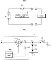
- FIG. 1 is a diagram schematically showing that a switch control circuit according to an embodiment of the present disclosure is connected to a switch provided at a battery pack.
- FIG. 2 is a diagram schematically showing that the switch control circuit according to an embodiment of the present disclosure is connected to the switch.
- the switch control apparatus may be included in a switch control circuit 1.
- the switch control circuit 1 may be a circuit for controlling a switch 10 provided between a positive electrode terminal of a cell assembly B including at least one secondary battery and a positive electrode terminal of a battery pack.
- the positive electrode terminal and the negative electrode terminal of the battery pack may be connected to a load L.
- both ends of the battery pack may be connected to a vehicle load.
- the switch control apparatus may include a freewheeling diode 100, a Zener diode 200, a field effect transistor (FET) 300, a control unit 400 and a resistor 500.
- FET field effect transistor
- the freewheeling diode 100 may be electrically connected to the switch 10 in parallel.
- the freewheeling diode 100 may be provided between the ground G and a first node N1 provided on a connection path between an input terminal Vi and the switch 10.
- the freewheeling diode 100 may be electrically connected in parallel to the switch 10 having both ends connected to the first node N1 and the ground G.
- the freewheeling diode 100 may be configured to allow a current to flow toward the positive electrode terminal of the switch 10.
- the freewheeling diode 100 may be a diode configured to allow a current to flow toward the first node N1 while setting the direction toward the first node N1 as a forward direction.
- the freewheeling diode 100 may be configured such that a current flows toward the positive electrode terminal of the switch 10 through the first node N1.
- the freewheeling diode 100 may allow the current generated by an inductor component of the switch 10 to flow back to the switch 10 through a closed loop that connects the freewheeling diode 100 and the switch 10, thereby preventing the switch 10 from being damaged by an impulse voltage generated by a counter electromotive force.
- the Zener diode 200 may be electrically connected to the freewheeling diode 100 in series.
- the Zener diode 200 may be provided between the first node N1 and the ground G and electrically connected to the freewheeling diode 100 in series.
- the Zener diode 200 may be configured so that its forward direction is a direction toward the ground G.
- the Zener diode 200 may be configured so that a direction toward the first node N1 is a reverse direction and a direction toward the ground G is a forward direction.
- the Zener diode 200 may allow a predetermined threshold voltage to be applied to the first node N1.
- a counter electromotive force may be generated due to an electromagnet provided in the switch 10.
- the ground G connected to the Zener diode 200 may instantaneously have a higher potential than the first node N1.
- -18V may be applied to the first node N1, relative to the ground G.
- the FET 300 may be provided between the input terminal Vi of the voltage input source and the positive electrode terminal of the switch 10.
- the FET 300 may be provided on a path connecting the input terminal Vi and the positive electrode terminal of the switch 10.
- the FET 300 may be configured such that a source terminal S of the FET 300 is electrically connected directly to the input terminal Vi and a drain terminal D of the FET 300 is electrically connected directly to the switch 10.
- the FET 300 may receive an input voltage from the input terminal Vi.
- the FET 300 may receive an input voltage from the input terminal Vi of the voltage input source to the source terminal S of the FET 300.
- the voltage input source may be a voltage source provided in a battery management system (BMS).
- BMS battery management system
- the voltage input source may be a 12V lead storage battery provided in the BMS.
- the FET 300 may be configured to transmit the input voltage input from the input terminal Vi of the voltage input source to the positive electrode terminal of the switch 10.
- the FET 300 may be configured to electrically connect the source terminal S of the FET 300 and the drain terminal D of the FET 300 to each other according to a signal applied to the gate terminal G of the FET 300.
- the FET 300 may transmit the input voltage from the source terminal S to the positive electrode terminal of the switch 10.
- the FET 300 may be a p-channel MOSFET (Metal Oxide Semiconductor Field Effect Transistor) having a parasitic diode.
- MOSFET Metal Oxide Semiconductor Field Effect Transistor
- the control unit 400 may be electrically connected to the FET 300.
- the control unit 400 may be electrically connected directly to the gate terminal G of the FET 300.
- control unit 400 may be configured to transmit a signal for controlling the opening/closing operation of the switch 10 to the FET 300. That is, in the configuration of FIG. 2 , the control unit 400 may transmit an electric signal to the gate terminal G of the FET 300. In addition, the control unit 400 may transmit a signal for controlling the opening/closing operation of the switch 10 to the gate terminal G of the FET 300.
- control unit 400 may apply a voltage of 0V to the gate terminal G of the FET 300 such that the FET 300 is in a closed state.
- control unit 400 may apply a voltage of 5V to the gate terminal G of the FET 300 such that the FET 300 is in an open state.
- 5V may be a threshold voltage of the FET 300.
- the control unit 400 may close the FET 300 by applying 0V to the gate terminal G of the FET 300.
- the input voltage may be transmitted from the voltage input source to the positive electrode terminal of the switch 10. Subsequently, switch 10 may be shifted to the closed state by receiving the input voltage.
- the control unit 400 may open the FET 300 by applying 5V to the gate terminal G of the FET 300.
- the input voltage may not be transmitted from the voltage input source to the positive electrode terminal of the switch 10. Subsequently, the switch 10 may be shifted to an open state.
- the resistor 500 may be provided on a connection path between the control unit 400 and the path along which the power is supplied from the input terminal Vi of the voltage input source to the switch 10.
- the resistor 500 may be provided on a connection path that connects a second node N2 and the control unit 400.
- the second node N2 may be provided on a path that connects the input terminal Vi and the positive electrode terminal of the switch 10 to each other.
- the second node N2 may be provided between the drain terminal D of the FET 300 and the first node N1.
- the resistor 500 may be configured to distribute the voltage applied to control unit 400. For example, as shown in FIG. 2 , a portion of the voltage applied between the second node N2 and the control unit 400 may be dividedly applied to the resistor 500. Through this configuration, the resistor 500 according to an embodiment of the present disclosure may prevent the voltage applied to the second node N2 from being entirely applied to the control unit 400.
- the control unit 400 may include at least two input/output pins i1, i2.
- the input/output pins i1, i2 may be configured to be electrically connected directly to the FET 300 and the resistor 500, respectively.
- the first input/output pin i1 may be an input/output pin that connects the second node N2 and the control unit 400 to each other.
- the first input/output pin i1 may be an input/output pin that electrically connects the resistor 500 and the control unit 400 directly.
- the second input/output pin i2 may be an input/output pin that directly connects the gate terminal G of the FET 300 and the control unit 400 to each other.
- the control unit 400 may measure a potential of the drain terminal D of the FET 300 through the second input/output pin i2 to diagnose whether the FET 300 is disconnected or short-circuited.
- the resistor 500 may be configured such that both ends thereof are electrically connected directly between the input/output pins of the control unit 400 and a node between the drain terminal D of the FET 300 and the positive electrode terminal of the switch 10.
- the resistor 500 may be configured such that both ends thereof are electrically connected directly between the second node N2 and the first input/output pin i1 of the control unit 400.
- the Zener diode 200 may be connected in series to the freewheeling diode 100.
- the Zener diode 200 may be electrically connected directly between the ground G and the freewheeling diode 100.
- the source terminal S of the FET 300 may be electrically connected directly to the input terminal Vi.
- the drain terminal D of the FET 300 may be electrically connected to the positive electrode terminal of the switch 10 directly.
- the gate terminal G of the FET 300 may be electrically connected directly to the control unit 400.
- FIG. 3 is a diagram schematically showing a battery pack to which the switch control circuit according to an embodiment of the present disclosure is provided.
- the switch 10 shown in FIGS. 1 and 2 may include an iron piece 11 and an electromagnet 12.
- the input terminal Vi may be a terminal at which a current is output from the voltage input source DC.
- the voltage input source DC may be a 12V lead storage battery.
- the positive electrode terminals of the cell assembly B and the battery pack may be connected to the iron piece 11 provided at the switch 10, and the switch control circuit 1 may be connected to the electromagnet 12 provided at the switch 10.
- the other end of the electromagnet 12 may be connected to the ground G connected to the other end of the voltage input source DC.
- the electromagnet 12 may include an iron core and a coil.
- the coil may be wound around the iron core.
- the switch 10 may be controlled to turn on. That is, if a 0V voltage is applied to the gate terminal G of the FET 300, the positive electrode terminal of the cell assembly 10 and the positive electrode terminal of the battery pack may be electrically connected.
- the connection between the source terminal S and the drain terminal D may be disconnected.
- a voltage greater than the operating voltage is applied to the gate terminal G of the FET 300
- the connection between the source terminal S and the drain terminal D may be disconnected.
- a counter electromotive force may be generated due to the electromagnet 12.
- the ground G connected to the electromagnet 12 and the Zener diode 200 instantly has a higher potential than the potential of the electromagnet 12 connected to the first node N1, so that the current generated by the counter electromotive force may flow to the ground G.
- the electromagnet 12, the ground G, the Zener diode 200 and the freewheeling diode 100 form a closed loop, and the current generated by the counter electromotive force may be quickly consumed while flowing through the formed closed loop.
- the current generated by the counter electromotive force flows in the closed loop, -18 V may be applied to the first node N1 relative to ground G.
- the resistor 500 may consume some of the current flowing to control unit 400 such that the voltage applied to the input/output pins of the control unit 400 falls within a rated voltage range of the control unit 400.
- the switch control apparatus may quickly release and consume the current caused by a counter electromotive force generated based on the change in the operating state of the switch 10.
- the switch control apparatus may maintain the voltage applied to the control unit within the rated voltage.
- the stability of the switch control circuit may be further enhanced.
- control unit 400 may be implemented to include a control unit 400, an application-specific integrated circuit (ASIC), another chipset, a logic circuit, a register, a communication modem, a data processing device, and/or a memory device, selectively.
- ASIC application-specific integrated circuit
- the memory device is not particularly limited as long as it serves as a storage medium capable of recording and erasing data.
- the memory device may be a random access memory (RAM), a read only memory (ROM), a register, a hard disk, an optical recording medium, or a magnetic recording medium.
- the memory device also be electrically connected to the control unit 400, for example, via a data bus or the like so as to be accessed by the control unit 400.
- the memory device may also store and/or update and/or erase and/or transmit data generated when a program including various control logics performed in the control unit 400 and/or a control logic is executed.
- FIG. 4 is a diagram schematically showing that a switch control circuit according to another embodiment of the present disclosure is connected to a switch.
- a feature to which the description of the former embodiment may be similarly applied will not be described, and description will be given focusing on different features.
- control unit 400 and the resistor 500 may be electrically connected directly at a node provided between the control unit 400 and the resistor 500.
- the switch control apparatus may further include a reverse voltage protection diode 600.
- the reverse voltage protection diode 600 may be connected to the node provided between the control unit 400 and the resistor 500.
- the reverse voltage protection diode 600 may be configured so that a forward direction thereof is a direction toward the resistor 500.
- the reverse voltage protection diode 600 may be electrically connected directly between the ground G and the node provided between the control unit 400 and the resistor 500.
- the reverse voltage protection diode 600 may be configured such that the forward direction is a direction toward the node provided between the control unit 400 and the resistor 500.
- the switch control apparatus according to the present disclosure may be applied to a battery management system (BMS). That is, the BMS according to the present disclosure may include the switch control apparatus of the present disclosure as described above. In this configuration, at least a part of the components of the switch control apparatus according to the present disclosure may be implemented by supplementing or adding functionality of components included in the conventional BMS. For example, the control unit 400 and the memory device of the switch control apparatus according to the present disclosure may be implemented as components of the BMS.
- the switch control apparatus may be provided to a battery pack. That is, the battery pack according to the present disclosure may include the switch control apparatus according to the present disclosure.
- the battery pack may include at least one secondary battery, the switch control apparatus, electrical components (such as a BMS, a relay and a fuse), a case, and so on.
- FIG. 5 is a diagram schematically showing a resistor connected between a control unit according to an embodiment of the present disclosure and a switch.
- the resistor 500 may be provided between the second node N2 and the first input/output pin i1 of the control unit 400.
- the control unit 400 may include an internal resistor 410, as shown in FIG. 5 .
- the internal resistor 410 may be provided between the first input/output pins i1 and an internal terminal il'.
- the internal resistor 410 may be an equivalent resistor 500 of the control unit 400.
- the resistor 500 may be configured such that the voltage applied to the input/output pins of the control unit 400 is applied within the rated voltage of the control unit 400.
- the voltage applied between the internal terminal i1' and the second node N2 is 18V and the internal resistor 410 and the resistor 500 have the same resistance of 1 kQ
- 18V may be distributed to the internal resistor 410 and the resistor 500, namely 9V for each.
- -9V may be applied to the first input/output pin i1.
- the resistor 500 may distribute the voltage applied to the second node N2 so that the voltage applied to the input/output pin of the control unit 400 falls with the rated voltage of the control unit 400.
- the resistor 500 may have a resistance greater than or equal to the resistance of the internal resistor of the control unit 400. Even when the resistance of the resistor 500 is greater than or equal to the resistance of the internal resistor 410, a voltage corresponding to the rated voltage of the control unit 400 may be stably applied to the first input/output pin i1. For example, if -18V is applied to the second node N2, the resistance of the resistor 500 is 2kQ, and the resistance of the internal resistor 410 is 1k ⁇ , -6V may be applied to the first input/output pin i1.
- the switch control apparatus quickly releases the current by the counter electromotive force generated when the switch is shifted from the closed state to the open state and allows the voltage applied to the control unit to be applied within the rated voltage. In this way, it is possible to prevent devices such as an IC chip provided in the control unit from being damaged.
- control logics of the control unit there is no particular limitation on the types of various control logics of the control unit, as long as one or more control logics are combined and the combined control logic is written in a computer-readable code system so that the computer-readable access is possible.
- the recording medium includes at least one selected from the group consisting of a ROM, a RAM, a register, a CD-ROM, a magnetic tape, a hard disk, a floppy disk and an optical data recording device.
- the code system may be stored and executed in a distributed manner on computers connected through a network.
- functional programs, code and segments for implementing the combined control logics may be easily inferred by programmers in the technical field to which the present disclosure belongs.
- 'unit' is used, such as 'control unit'.
- 'control unit' just represent logical configuration units and are not intended to represent components that are physically separable or must be physically separated.
Landscapes
- Engineering & Computer Science (AREA)
- Power Engineering (AREA)
- Mechanical Engineering (AREA)
- Sustainable Development (AREA)
- Sustainable Energy (AREA)
- Transportation (AREA)
- Life Sciences & Earth Sciences (AREA)
- Theoretical Computer Science (AREA)
- Physics & Mathematics (AREA)
- General Engineering & Computer Science (AREA)
- General Physics & Mathematics (AREA)
- Charge And Discharge Circuits For Batteries Or The Like (AREA)
- Electronic Switches (AREA)
- Emergency Protection Circuit Devices (AREA)
- Electric Propulsion And Braking For Vehicles (AREA)
Applications Claiming Priority (2)
| Application Number | Priority Date | Filing Date | Title |
|---|---|---|---|
| KR1020180094441A KR102423888B1 (ko) | 2018-08-13 | 2018-08-13 | 스위치 제어 장치 |
| PCT/KR2019/010333 WO2020036427A1 (fr) | 2018-08-13 | 2019-08-13 | Dispositif de commande de commutateur |
Publications (2)
| Publication Number | Publication Date |
|---|---|
| EP3753779A1 true EP3753779A1 (fr) | 2020-12-23 |
| EP3753779A4 EP3753779A4 (fr) | 2021-08-25 |
Family
ID=69525692
Family Applications (1)
| Application Number | Title | Priority Date | Filing Date |
|---|---|---|---|
| EP19850305.4A Pending EP3753779A4 (fr) | 2018-08-13 | 2019-08-13 | Dispositif de commande de commutateur |
Country Status (6)
| Country | Link |
|---|---|
| US (1) | US11072257B2 (fr) |
| EP (1) | EP3753779A4 (fr) |
| JP (1) | JP7078292B2 (fr) |
| KR (1) | KR102423888B1 (fr) |
| CN (1) | CN111629928B (fr) |
| WO (1) | WO2020036427A1 (fr) |
Families Citing this family (4)
| Publication number | Priority date | Publication date | Assignee | Title |
|---|---|---|---|---|
| KR102784127B1 (ko) * | 2020-07-30 | 2025-03-19 | 주식회사 엘지에너지솔루션 | 인터락 회로를 이용한 msd 대체 안전장치 |
| KR102842675B1 (ko) * | 2022-09-05 | 2025-08-05 | 주식회사 현대케피코 | 비선형 차량 센서 입력에 대한 오차 보정 장치 및 그 방법 |
| CN115663776B (zh) * | 2022-11-04 | 2026-03-03 | 深圳朗特智能控制股份有限公司 | 一种电池接口电路 |
| CN116811657B (zh) * | 2023-05-12 | 2026-01-13 | 宁德时代新能源科技股份有限公司 | 电池控制方法、装置、电池管理系统和存储介质 |
Family Cites Families (34)
| Publication number | Priority date | Publication date | Assignee | Title |
|---|---|---|---|---|
| JPS4721147U (fr) * | 1971-03-17 | 1972-11-09 | ||
| JPS55119320A (en) * | 1979-03-09 | 1980-09-13 | Fujikoshi Kk | Overvoltage preventive relay contact protector |
| JPS58174946U (ja) * | 1982-05-18 | 1983-11-22 | 三菱電機株式会社 | サ−ジ吸収回路 |
| EP0827170B1 (fr) * | 1996-07-31 | 2004-11-03 | Matsushita Electric Works, Ltd. | Dispositif d'entraínement d'un eléctro-aimant |
| KR100264146B1 (ko) | 1997-10-23 | 2000-08-16 | 이종수 | 전자접촉기의 코일구동장치 |
| JP3660186B2 (ja) * | 1999-02-14 | 2005-06-15 | 矢崎総業株式会社 | 半導体装置 |
| JP3632517B2 (ja) | 1999-08-06 | 2005-03-23 | 株式会社デンソー | 誘導性負荷の駆動装置 |
| JP2001270401A (ja) | 2000-03-24 | 2001-10-02 | Nippon Densan Corp | 車載用モータの制御装置 |
| US6657839B2 (en) | 2000-08-25 | 2003-12-02 | Tyco Electronics Corporation | Protective relay |
| KR100434153B1 (ko) | 2002-04-12 | 2004-06-04 | 엘지산전 주식회사 | 하이브리드 직류 전자 접촉기 |
| JP2005029020A (ja) * | 2003-07-14 | 2005-02-03 | Ichikoh Ind Ltd | スイッチング回路及び車両用灯具の電子発光素子駆動回路 |
| JP5084526B2 (ja) | 2008-01-22 | 2012-11-28 | 三洋電機株式会社 | 車両用の電源装置 |
| JP5241540B2 (ja) * | 2009-01-30 | 2013-07-17 | 日立オートモティブシステムズ株式会社 | 車載制御装置 |
| JP5317188B2 (ja) * | 2009-02-20 | 2013-10-16 | 株式会社安川電機 | 電動車両のインバータ装置及びその保護方法 |
| KR101031586B1 (ko) | 2009-06-24 | 2011-04-27 | 넥스콘 테크놀러지 주식회사 | 전기자동차용 고전압 배터리팩의 메인 커넥터 점검 회로 |
| JP5303495B2 (ja) * | 2010-03-09 | 2013-10-02 | 矢崎総業株式会社 | 電磁誘導負荷の制御装置 |
| JP5486396B2 (ja) * | 2010-05-11 | 2014-05-07 | ルネサスエレクトロニクス株式会社 | 負荷駆動回路 |
| KR101413251B1 (ko) * | 2010-08-13 | 2014-06-27 | 주식회사 엘지화학 | 2차 전지 관리 장치 |
| US8810287B2 (en) * | 2011-01-14 | 2014-08-19 | Panasonic Corporation | Driver for semiconductor switch element |
| US8861164B2 (en) | 2011-02-04 | 2014-10-14 | Fairchild Semiconductor Corporation | Integrated overdrive and overvoltage protection device |
| FR2977986B1 (fr) * | 2011-07-13 | 2014-04-25 | Commissariat Energie Atomique | Batterie avec architecture en briques disposees en serie ou en parallele |
| JP5947676B2 (ja) * | 2012-08-31 | 2016-07-06 | 矢崎総業株式会社 | スイッチング方法及びその装置 |
| KR20140055986A (ko) | 2012-10-31 | 2014-05-09 | 대성전기공업 주식회사 | 스위치 릴레이 장치 |
| US9660244B2 (en) * | 2013-09-06 | 2017-05-23 | Johnson Controls Technology Company | System and method for establishing connections of a battery module |
| JP6425380B2 (ja) | 2013-12-26 | 2018-11-21 | ローム株式会社 | パワー回路およびパワーモジュール |
| JP6448655B2 (ja) * | 2014-02-17 | 2019-01-09 | エルジー・ケム・リミテッド | 故障発生如何を分析可能な信号を出力するバッテリー管理システム及びそれを含むバッテリー駆動システム |
| KR20160029931A (ko) | 2014-09-05 | 2016-03-16 | 화남전자 주식회사 | 자동 손상 인식 구조를 갖는 플래셔 시스템 |
| KR101796431B1 (ko) * | 2015-09-08 | 2017-11-09 | 유수근 | 역률 보상형 led 구동장치 및 구동방법 |
| JP6666130B2 (ja) | 2015-12-14 | 2020-03-13 | 株式会社エンビジョンAescジャパン | 制御装置および制御方法 |
| KR102253458B1 (ko) * | 2016-04-28 | 2021-05-17 | 로무 가부시키가이샤 | 과전류 보호 회로 |
| KR102145524B1 (ko) * | 2016-06-22 | 2020-08-18 | 주식회사 엘지화학 | 전기 자동차용 구동 회로 및 그 제어 방법 |
| KR102610269B1 (ko) * | 2016-09-05 | 2023-12-04 | 주식회사 엘지에너지솔루션 | 전력 공급 회로 및 이를 포함하는 배터리 팩 |
| KR102632405B1 (ko) | 2016-11-04 | 2024-01-31 | 한국전기연구원 | 고장전류 저감회로를 포함하는 집합전지 시스템 |
| KR20180094441A (ko) | 2017-02-15 | 2018-08-23 | 인제대학교 산학협력단 | 웨이퍼 보관함 |
-
2018
- 2018-08-13 KR KR1020180094441A patent/KR102423888B1/ko active Active
-
2019
- 2019-08-13 US US16/961,978 patent/US11072257B2/en active Active
- 2019-08-13 JP JP2020538696A patent/JP7078292B2/ja active Active
- 2019-08-13 CN CN201980007998.9A patent/CN111629928B/zh active Active
- 2019-08-13 EP EP19850305.4A patent/EP3753779A4/fr active Pending
- 2019-08-13 WO PCT/KR2019/010333 patent/WO2020036427A1/fr not_active Ceased
Also Published As
| Publication number | Publication date |
|---|---|
| JP2021511715A (ja) | 2021-05-06 |
| KR20200018958A (ko) | 2020-02-21 |
| EP3753779A4 (fr) | 2021-08-25 |
| US20210078437A1 (en) | 2021-03-18 |
| WO2020036427A1 (fr) | 2020-02-20 |
| KR102423888B1 (ko) | 2022-07-20 |
| CN111629928A (zh) | 2020-09-04 |
| CN111629928B (zh) | 2023-08-15 |
| JP7078292B2 (ja) | 2022-05-31 |
| US11072257B2 (en) | 2021-07-27 |
Similar Documents
| Publication | Publication Date | Title |
|---|---|---|
| US11205804B2 (en) | BMS wake-up device, and BMS and battery pack including same | |
| KR102412313B1 (ko) | 스위치 진단 장치 및 방법 | |
| US11204387B2 (en) | Apparatus for diagnosing relay driving circuit | |
| US11271412B2 (en) | Battery management system, battery pack and electric vehicle | |
| US11072257B2 (en) | Switch control apparatus | |
| US11293985B2 (en) | Switch diagnosing apparatus and method | |
| KR102364237B1 (ko) | 프리차지 장치 및 방법 | |
| US11258274B2 (en) | Apparatus and method for battery module balancing | |
| US11255915B2 (en) | Switch control apparatus and method | |
| KR102817147B1 (ko) | 스위치 제어 장치 | |
| KR20200004650A (ko) | 듀얼 배터리 프리차지 장치 및 방법 | |
| US11919402B2 (en) | Relay control apparatus and method | |
| KR20200038818A (ko) | 전류 센서 진단 장치 및 방법 | |
| EP4135101A1 (fr) | Dispositif de gestion de batterie | |
| US20230369877A1 (en) | Battery management apparatus and battery system including the same | |
| KR102829280B1 (ko) | 배터리 스위칭 장치 | |
| US11929740B2 (en) | Relay control apparatus | |
| KR102593366B1 (ko) | 다중 신호 측정 시스템 및 방법 |
Legal Events
| Date | Code | Title | Description |
|---|---|---|---|
| STAA | Information on the status of an ep patent application or granted ep patent |
Free format text: STATUS: THE INTERNATIONAL PUBLICATION HAS BEEN MADE |
|
| PUAI | Public reference made under article 153(3) epc to a published international application that has entered the european phase |
Free format text: ORIGINAL CODE: 0009012 |
|
| STAA | Information on the status of an ep patent application or granted ep patent |
Free format text: STATUS: REQUEST FOR EXAMINATION WAS MADE |
|
| 17P | Request for examination filed |
Effective date: 20200918 |
|
| AK | Designated contracting states |
Kind code of ref document: A1 Designated state(s): AL AT BE BG CH CY CZ DE DK EE ES FI FR GB GR HR HU IE IS IT LI LT LU LV MC MK MT NL NO PL PT RO RS SE SI SK SM TR |
|
| AX | Request for extension of the european patent |
Extension state: BA ME |
|
| A4 | Supplementary search report drawn up and despatched |
Effective date: 20210727 |
|
| RIC1 | Information provided on ipc code assigned before grant |
Ipc: B60L 58/19 20190101AFI20210721BHEP Ipc: B60L 58/21 20190101ALI20210721BHEP Ipc: H03K 17/0814 20060101ALI20210721BHEP Ipc: H02J 7/00 20060101ALI20210721BHEP Ipc: H01H 47/32 20060101ALI20210721BHEP |
|
| DAV | Request for validation of the european patent (deleted) | ||
| DAX | Request for extension of the european patent (deleted) | ||
| RAP1 | Party data changed (applicant data changed or rights of an application transferred) |
Owner name: LG ENERGY SOLUTION LTD. |
|
| RAP3 | Party data changed (applicant data changed or rights of an application transferred) |
Owner name: LG ENERGY SOLUTION, LTD. |
|
| STAA | Information on the status of an ep patent application or granted ep patent |
Free format text: STATUS: EXAMINATION IS IN PROGRESS |
|
| 17Q | First examination report despatched |
Effective date: 20250603 |
|
| GRAP | Despatch of communication of intention to grant a patent |
Free format text: ORIGINAL CODE: EPIDOSNIGR1 |
|
| STAA | Information on the status of an ep patent application or granted ep patent |
Free format text: STATUS: GRANT OF PATENT IS INTENDED |