EP3758048B1 - Eine bindungsübergangsstruktur - Google Patents
Eine bindungsübergangsstruktur Download PDFInfo
- Publication number
- EP3758048B1 EP3758048B1 EP20186997.1A EP20186997A EP3758048B1 EP 3758048 B1 EP3758048 B1 EP 3758048B1 EP 20186997 A EP20186997 A EP 20186997A EP 3758048 B1 EP3758048 B1 EP 3758048B1
- Authority
- EP
- European Patent Office
- Prior art keywords
- copper
- bonding
- support
- die
- copper powder
- Prior art date
- Legal status (The legal status is an assumption and is not a legal conclusion. Google has not performed a legal analysis and makes no representation as to the accuracy of the status listed.)
- Active
Links
Images


Classifications
-
- H—ELECTRICITY
- H10—SEMICONDUCTOR DEVICES; ELECTRIC SOLID-STATE DEVICES NOT OTHERWISE PROVIDED FOR
- H10W—GENERIC PACKAGES, INTERCONNECTIONS, CONNECTORS OR OTHER CONSTRUCTIONAL DETAILS OF DEVICES COVERED BY CLASS H10
- H10W72/00—Interconnections or connectors in packages
- H10W72/071—Connecting or disconnecting
-
- B—PERFORMING OPERATIONS; TRANSPORTING
- B22—CASTING; POWDER METALLURGY
- B22F—WORKING METALLIC POWDER; MANUFACTURE OF ARTICLES FROM METALLIC POWDER; MAKING METALLIC POWDER; APPARATUS OR DEVICES SPECIALLY ADAPTED FOR METALLIC POWDER
- B22F7/00—Manufacture of composite layers, workpieces, or articles, comprising metallic powder, by sintering the powder, with or without compacting wherein at least one part is obtained by sintering or compression
- B22F7/06—Manufacture of composite layers, workpieces, or articles, comprising metallic powder, by sintering the powder, with or without compacting wherein at least one part is obtained by sintering or compression of composite workpieces or articles from parts, e.g. to form tipped tools
- B22F7/08—Manufacture of composite layers, workpieces, or articles, comprising metallic powder, by sintering the powder, with or without compacting wherein at least one part is obtained by sintering or compression of composite workpieces or articles from parts, e.g. to form tipped tools with one or more parts not made from powder
-
- C—CHEMISTRY; METALLURGY
- C09—DYES; PAINTS; POLISHES; NATURAL RESINS; ADHESIVES; COMPOSITIONS NOT OTHERWISE PROVIDED FOR; APPLICATIONS OF MATERIALS NOT OTHERWISE PROVIDED FOR
- C09K—MATERIALS FOR MISCELLANEOUS APPLICATIONS, NOT PROVIDED FOR ELSEWHERE
- C09K5/00—Heat-transfer, heat-exchange or heat-storage materials, e.g. refrigerants; Materials for the production of heat or cold by chemical reactions other than by combustion
- C09K5/08—Materials not undergoing a change of physical state when used
- C09K5/14—Solid materials, e.g. powdery or granular
-
- H—ELECTRICITY
- H10—SEMICONDUCTOR DEVICES; ELECTRIC SOLID-STATE DEVICES NOT OTHERWISE PROVIDED FOR
- H10P—GENERIC PROCESSES OR APPARATUS FOR THE MANUFACTURE OR TREATMENT OF DEVICES COVERED BY CLASS H10
- H10P14/00—Formation of materials, e.g. in the shape of layers or pillars
- H10P14/20—Formation of materials, e.g. in the shape of layers or pillars of semiconductor materials
- H10P14/29—Formation of materials, e.g. in the shape of layers or pillars of semiconductor materials characterised by the substrates
- H10P14/2926—Crystal orientations
-
- H—ELECTRICITY
- H10—SEMICONDUCTOR DEVICES; ELECTRIC SOLID-STATE DEVICES NOT OTHERWISE PROVIDED FOR
- H10P—GENERIC PROCESSES OR APPARATUS FOR THE MANUFACTURE OR TREATMENT OF DEVICES COVERED BY CLASS H10
- H10P95/00—Generic processes or apparatus for manufacture or treatments not covered by the other groups of this subclass
- H10P95/90—Thermal treatments, e.g. annealing or sintering
-
- H—ELECTRICITY
- H10—SEMICONDUCTOR DEVICES; ELECTRIC SOLID-STATE DEVICES NOT OTHERWISE PROVIDED FOR
- H10W—GENERIC PACKAGES, INTERCONNECTIONS, CONNECTORS OR OTHER CONSTRUCTIONAL DETAILS OF DEVICES COVERED BY CLASS H10
- H10W40/00—Arrangements for thermal protection or thermal control
- H10W40/10—Arrangements for heating
-
- H—ELECTRICITY
- H10—SEMICONDUCTOR DEVICES; ELECTRIC SOLID-STATE DEVICES NOT OTHERWISE PROVIDED FOR
- H10W—GENERIC PACKAGES, INTERCONNECTIONS, CONNECTORS OR OTHER CONSTRUCTIONAL DETAILS OF DEVICES COVERED BY CLASS H10
- H10W70/00—Package substrates; Interposers; Redistribution layers [RDL]
- H10W70/40—Leadframes
- H10W70/411—Chip-supporting parts, e.g. die pads
- H10W70/417—Bonding materials between chips and die pads
-
- H—ELECTRICITY
- H10—SEMICONDUCTOR DEVICES; ELECTRIC SOLID-STATE DEVICES NOT OTHERWISE PROVIDED FOR
- H10W—GENERIC PACKAGES, INTERCONNECTIONS, CONNECTORS OR OTHER CONSTRUCTIONAL DETAILS OF DEVICES COVERED BY CLASS H10
- H10W72/00—Interconnections or connectors in packages
- H10W72/071—Connecting or disconnecting
- H10W72/073—Connecting or disconnecting of die-attach connectors
-
- H—ELECTRICITY
- H10—SEMICONDUCTOR DEVICES; ELECTRIC SOLID-STATE DEVICES NOT OTHERWISE PROVIDED FOR
- H10W—GENERIC PACKAGES, INTERCONNECTIONS, CONNECTORS OR OTHER CONSTRUCTIONAL DETAILS OF DEVICES COVERED BY CLASS H10
- H10W72/00—Interconnections or connectors in packages
- H10W72/20—Bump connectors, e.g. solder bumps or copper pillars; Dummy bumps; Thermal bumps
-
- H—ELECTRICITY
- H10—SEMICONDUCTOR DEVICES; ELECTRIC SOLID-STATE DEVICES NOT OTHERWISE PROVIDED FOR
- H10W—GENERIC PACKAGES, INTERCONNECTIONS, CONNECTORS OR OTHER CONSTRUCTIONAL DETAILS OF DEVICES COVERED BY CLASS H10
- H10W72/00—Interconnections or connectors in packages
- H10W72/30—Die-attach connectors
-
- H—ELECTRICITY
- H10—SEMICONDUCTOR DEVICES; ELECTRIC SOLID-STATE DEVICES NOT OTHERWISE PROVIDED FOR
- H10W—GENERIC PACKAGES, INTERCONNECTIONS, CONNECTORS OR OTHER CONSTRUCTIONAL DETAILS OF DEVICES COVERED BY CLASS H10
- H10W72/00—Interconnections or connectors in packages
- H10W72/071—Connecting or disconnecting
- H10W72/073—Connecting or disconnecting of die-attach connectors
- H10W72/07331—Connecting techniques
-
- H—ELECTRICITY
- H10—SEMICONDUCTOR DEVICES; ELECTRIC SOLID-STATE DEVICES NOT OTHERWISE PROVIDED FOR
- H10W—GENERIC PACKAGES, INTERCONNECTIONS, CONNECTORS OR OTHER CONSTRUCTIONAL DETAILS OF DEVICES COVERED BY CLASS H10
- H10W72/00—Interconnections or connectors in packages
- H10W72/071—Connecting or disconnecting
- H10W72/073—Connecting or disconnecting of die-attach connectors
- H10W72/07351—Connecting or disconnecting of die-attach connectors characterised by changes in properties of the die-attach connectors during connecting
- H10W72/07355—Connecting or disconnecting of die-attach connectors characterised by changes in properties of the die-attach connectors during connecting changes in materials
-
- H—ELECTRICITY
- H10—SEMICONDUCTOR DEVICES; ELECTRIC SOLID-STATE DEVICES NOT OTHERWISE PROVIDED FOR
- H10W—GENERIC PACKAGES, INTERCONNECTIONS, CONNECTORS OR OTHER CONSTRUCTIONAL DETAILS OF DEVICES COVERED BY CLASS H10
- H10W72/00—Interconnections or connectors in packages
- H10W72/30—Die-attach connectors
- H10W72/321—Structures or relative sizes of die-attach connectors
- H10W72/325—Die-attach connectors having a filler embedded in a matrix
-
- H—ELECTRICITY
- H10—SEMICONDUCTOR DEVICES; ELECTRIC SOLID-STATE DEVICES NOT OTHERWISE PROVIDED FOR
- H10W—GENERIC PACKAGES, INTERCONNECTIONS, CONNECTORS OR OTHER CONSTRUCTIONAL DETAILS OF DEVICES COVERED BY CLASS H10
- H10W72/00—Interconnections or connectors in packages
- H10W72/30—Die-attach connectors
- H10W72/351—Materials of die-attach connectors
- H10W72/352—Materials of die-attach connectors comprising metals or metalloids, e.g. solders
- H10W72/3528—Intermetallic compounds
-
- H—ELECTRICITY
- H10—SEMICONDUCTOR DEVICES; ELECTRIC SOLID-STATE DEVICES NOT OTHERWISE PROVIDED FOR
- H10W—GENERIC PACKAGES, INTERCONNECTIONS, CONNECTORS OR OTHER CONSTRUCTIONAL DETAILS OF DEVICES COVERED BY CLASS H10
- H10W72/00—Interconnections or connectors in packages
- H10W72/30—Die-attach connectors
- H10W72/351—Materials of die-attach connectors
- H10W72/353—Materials of die-attach connectors not comprising solid metals or solid metalloids, e.g. ceramics
- H10W72/354—Materials of die-attach connectors not comprising solid metals or solid metalloids, e.g. ceramics comprising polymers
-
- H—ELECTRICITY
- H10—SEMICONDUCTOR DEVICES; ELECTRIC SOLID-STATE DEVICES NOT OTHERWISE PROVIDED FOR
- H10W—GENERIC PACKAGES, INTERCONNECTIONS, CONNECTORS OR OTHER CONSTRUCTIONAL DETAILS OF DEVICES COVERED BY CLASS H10
- H10W72/00—Interconnections or connectors in packages
- H10W72/50—Bond wires
- H10W72/59—Bond pads specially adapted therefor
-
- H—ELECTRICITY
- H10—SEMICONDUCTOR DEVICES; ELECTRIC SOLID-STATE DEVICES NOT OTHERWISE PROVIDED FOR
- H10W—GENERIC PACKAGES, INTERCONNECTIONS, CONNECTORS OR OTHER CONSTRUCTIONAL DETAILS OF DEVICES COVERED BY CLASS H10
- H10W72/00—Interconnections or connectors in packages
- H10W72/60—Strap connectors, e.g. thick copper clips for grounding of power devices
- H10W72/651—Materials of strap connectors
- H10W72/652—Materials of strap connectors comprising metals or metalloids, e.g. silver
-
- H—ELECTRICITY
- H10—SEMICONDUCTOR DEVICES; ELECTRIC SOLID-STATE DEVICES NOT OTHERWISE PROVIDED FOR
- H10W—GENERIC PACKAGES, INTERCONNECTIONS, CONNECTORS OR OTHER CONSTRUCTIONAL DETAILS OF DEVICES COVERED BY CLASS H10
- H10W72/00—Interconnections or connectors in packages
- H10W72/90—Bond pads, in general
- H10W72/951—Materials of bond pads
- H10W72/952—Materials of bond pads comprising metals or metalloids, e.g. PbSn, Ag or Cu
Definitions
- the copper powder P has a crystallite diameter of preferably not more than 60 nm, more preferably not more than 50 nm, and even more preferably not more than 40 nm.
- the lower limit value of the crystallite diameter is preferably 20 nm.
- the low-temperature sinterability of the copper powder can be improved even more by setting the size of the crystallite diameter within this range.
- the crystallite diameter is obtained by performing X-ray diffraction measurement of the copper powder using a RINT-TTR III manufactured by Rigaku Corporation, for example, and calculating the crystallite diameter (nm) according to a Scherrer method using the obtained ⁇ 111 ⁇ peak.
- the above-described sintering onset temperature can be measured by allowing the copper powder P to stand in a furnace with a 3 vol% H 2 -N 2 atmosphere and gradually increasing the temperature in the furnace. Specifically, the sintering onset temperature can be measured using a method that will be described below. Whether or not sintering has started is judged by observing the copper powder P taken out of the furnace, under a scanning electron microscope to see if surface association has occurred between particles. "Surface association" refers to a state in which particles are connected to each other such that the surface of a particle is continuous with the surface of another particle.
- the "plurality of times” is preferably between about 2 times and 6 times inclusive.
- the intervals between additions of hydrazine are preferably between about 5 minutes and 90 minutes inclusive.
- a 500-ml round-bottomed flask provided with a stirring blade was prepared.
- As a copper source 15.71 g of copper acetate monohydrate was put into this round-bottomed flask.
- 10 g of water and 70.65 g of isopropanol serving as an organic solvent were put into this round-bottomed flask to obtain a reaction mixture.
- This reaction mixture was heated to 60 °C while being stirred at 150 rpm. While stirring was continued, 1.97 g of hydrazine monohydrate was added to the reaction mixture all at once. Then, the reaction mixture was stirred for 30 minutes. After that, 17.73 g of hydrazine monohydrate was added to the reaction mixture. The reaction mixture was further stirred for 30 minutes.
- a mixed copper powder was used in which a copper powder composed of copper particles formed through wet synthesis, namely, 1050Y (trade name) manufactured by Mitsui Mining & Smelting Co., Ltd. and a copper powder composed of copper particles formed through wet synthesis, namely, 1300Y (trade name) manufactured by Mitsui Mining & Smelting Co., Ltd. were mixed in a mass ratio of 56:44.
- RE-303SL which is a bisphenol F type epoxy resin manufactured by Nippon Kayaku Co., Ltd., RE-306, which is a phenol novolac type epoxy resin manufactured by Nippon Kayaku Co., Ltd.
- RE-310S which is a bisphenol A type epoxy resin manufactured by Nippon Kayaku Co., Ltd.
- GAN which is a liquid type epoxy resin manufactured by Nippon Kayaku Co., Ltd.
- KAYAHARD MCD which is a hardener manufactured by Nippon Kayaku Co., Ltd., 2-(3,4-epoxycyclohexyl)ethyltrimethylsilane, 3-glycidoxypropyltrimethoxysilane, and Amicure MY24, which is a curing accelerator manufactured by Ajinomoto Fine-Techno Co., Inc., were mixed.
- the mixed copper powder and the mixed resin were mixed to prepare a copper paste.
- the mixed resin contained 31% RE-303SL, 15% RE-306, 15% RE-310S, 6% GAN, 28% KAYAHARD MCD, 1% 2-(3,4-epoxycyclohexyl)ethyltrimethylsilane, 1% 3-glycidoxypropyltrimethoxysilane, and 3% Amicure MY24.
- the copper paste contained 89% mixed copper powder and 11% mixed resin.
- a bonding structure was formed in the same manner as in (2) of Example 2.
- the obtained bonding structure did not have enough mechanical strength to maintain the bonding between the die, the sintered body, and the support, and it was not possible to evaluate the heat dissipation properties of the obtained bonding structure and to determine the element distribution in the depth direction of a portion in the vicinity of the bonding interface between the sintered body and the support of the obtained bonding structure.
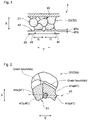
- Table 1 shows the results with respect to the above-described example and comparative examples regarding the die bonding joining structures with the structure shown in Fig. 1 .
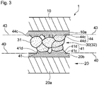
- Table 2 shows the results with respect to the above-described example and comparative examples regarding the die bonding joining structures with the structure shown in Fig. 3 .
- Blackening treatment of a back surface, that is, a surface on which the die was not placed, of the support of each bonding structure was performed by applying a carbon spray to that surface. Then, this surface was irradiated with a pulsed laser beam at 3 kV using a thermal constant measurement apparatus TC-7000 manufactured by Shinku-Riko Inc., and a change in the surface temperature of the die over time after irradiation was measured using a thermocouple. The time t (1/2) taken for this temperature to rise by 1/2 of a temperature rise amount ⁇ T was calculated from the measurement results and used as an index for evaluation of the heat dissipation properties.
- the silver paste was applied to a support formed of a 15-mm-square silver plate (99.98% purity) with a thickness of 0.1 mm through screen printing using a metal mask with a thickness of 50 ⁇ m such that the applied silver paste was formed into a shape 10 mm square.
- a 10-mm-square silver plate (99.98% purity) with a thickness of 0.1 mm was placed on the center of the support as a die.
- the temperature was increased to 300 °C at a rate of 5 °C/min in air and was kept for 30 minutes to give a target bonding structure.
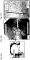
- Fig. 8 shows TEM images of a portion in the vicinity of the bonding interface between the sintered body and the support of the obtained bonding structure. As is clear from Fig.
Landscapes
- Chemical & Material Sciences (AREA)
- Engineering & Computer Science (AREA)
- Materials Engineering (AREA)
- Manufacturing & Machinery (AREA)
- Composite Materials (AREA)
- Mechanical Engineering (AREA)
- Combustion & Propulsion (AREA)
- Thermal Sciences (AREA)
- Chemical Kinetics & Catalysis (AREA)
- Organic Chemistry (AREA)
- Physics & Mathematics (AREA)
- Powder Metallurgy (AREA)
- Die Bonding (AREA)
- Crystallography & Structural Chemistry (AREA)
- Manufacture Of Metal Powder And Suspensions Thereof (AREA)
Claims (1)
- Bondverbindungsstruktur (1), bei der ein wärmeerzeugender Körper und ein Träger (20) umfassend ein Metall über einen Verbindungsabschnitt (30) miteinander verbunden sind, der aus einem Sinterkörper (32) aus Kupferpulver zusammengesetzt ist, der nur aus Kupfer zusammengesetzt ist,wobei die Bondverbindungsstruktur (1) eine Chipbondverbindungsstruktur ist, in der ein Chip einer Halbleitervorrichtung (10) als der wärmeerzeugende Körper dient,die äußerste Oberfläche des Trägers (20) nur aus Kupfer zusammengesetzt ist,Interdiffusionsabschnitte (41), in denen in dem Träger (20) enthaltenes Kupfer und in dem Sinterkörper (32) enthaltenes Kupfer zueinander diffundiert sind, so ausgebildet sind, dass sie eine Bondgrenzfläche (40) zwischen dem Träger (20) und dem Sinterkörper (32) überspannen,die Interdiffusionsabschnitte (41) jeweils eine einzelne Phase enthalten, die durch eine Kristallstruktur gebildet ist, die nur aus Kupfer besteht, undeine Kupferkristallstruktur mit derselben Kristallorientierung in jedem Interdiffusionsabschnitt (41) so ausgebildet ist, dass sie die Bondgrenzfläche (40) überspannt;wobei eine Goldschicht, die nur aus Gold zusammengesetzt ist, auf einer unteren Oberfläche des Chips (10) gebildet ist, Interdiffusionsabschnitte (44), in denen Gold, das in der unteren Oberfläche des Chips (10) enthalten ist, und Kupfer, das in dem Sinterkörper (32) enthalten ist, zueinander diffundiert sind, so ausgebildet sind, dass sie eine Bondgrenzfläche (43) zwischen dem Chip (10) und dem Sinterkörper (32) überspannen, unddie Interdiffusionsabschnitte (44) Cu3Au und eine feste Lösung aus Gold und Kupfer enthalten.
Applications Claiming Priority (3)
| Application Number | Priority Date | Filing Date | Title |
|---|---|---|---|
| JP2015196957 | 2015-10-02 | ||
| EP16851816.5A EP3358610B1 (de) | 2015-10-02 | 2016-09-29 | Eine bindungsübergangsstruktur |
| PCT/JP2016/078946 WO2017057645A1 (ja) | 2015-10-02 | 2016-09-29 | ボンディング接合構造 |
Related Parent Applications (2)
| Application Number | Title | Priority Date | Filing Date |
|---|---|---|---|
| EP16851816.5A Division EP3358610B1 (de) | 2015-10-02 | 2016-09-29 | Eine bindungsübergangsstruktur |
| EP16851816.5A Division-Into EP3358610B1 (de) | 2015-10-02 | 2016-09-29 | Eine bindungsübergangsstruktur |
Publications (2)
| Publication Number | Publication Date |
|---|---|
| EP3758048A1 EP3758048A1 (de) | 2020-12-30 |
| EP3758048B1 true EP3758048B1 (de) | 2022-11-09 |
Family
ID=58423967
Family Applications (2)
| Application Number | Title | Priority Date | Filing Date |
|---|---|---|---|
| EP20186997.1A Active EP3758048B1 (de) | 2015-10-02 | 2016-09-29 | Eine bindungsübergangsstruktur |
| EP16851816.5A Active EP3358610B1 (de) | 2015-10-02 | 2016-09-29 | Eine bindungsübergangsstruktur |
Family Applications After (1)
| Application Number | Title | Priority Date | Filing Date |
|---|---|---|---|
| EP16851816.5A Active EP3358610B1 (de) | 2015-10-02 | 2016-09-29 | Eine bindungsübergangsstruktur |
Country Status (7)
| Country | Link |
|---|---|
| US (1) | US10340154B2 (de) |
| EP (2) | EP3758048B1 (de) |
| JP (1) | JP6735764B2 (de) |
| KR (1) | KR102588747B1 (de) |
| CN (1) | CN108028206B (de) |
| TW (1) | TWI739763B (de) |
| WO (1) | WO2017057645A1 (de) |
Families Citing this family (22)
| Publication number | Priority date | Publication date | Assignee | Title |
|---|---|---|---|---|
| JP6699584B2 (ja) * | 2017-02-14 | 2020-05-27 | トヨタ自動車株式会社 | 導電性ペースト層と給電部を備えた樹脂部材の製造方法、および導電性ペースト層と給電部を備えた樹脂部材と外部給電部材の接続方法 |
| JP6936595B2 (ja) * | 2017-03-15 | 2021-09-15 | 株式会社 日立パワーデバイス | 半導体装置 |
| CN110431657A (zh) * | 2017-03-24 | 2019-11-08 | 三菱电机株式会社 | 半导体装置及其制造方法 |
| KR20190096731A (ko) * | 2018-02-09 | 2019-08-20 | 현대자동차주식회사 | 반도체 장치용 소결 접합 방법 |
| KR20210020937A (ko) * | 2018-06-15 | 2021-02-24 | 다우 글로벌 테크놀로지스 엘엘씨 | 강화 에폭시 조성물 |
| US11488841B2 (en) * | 2019-02-20 | 2022-11-01 | Electronics And Telecommunications Research Institute | Method for manufacturing semiconductor package |
| KR102564761B1 (ko) | 2019-03-07 | 2023-08-07 | 앱솔릭스 인코포레이티드 | 패키징 기판 및 이를 포함하는 반도체 장치 |
| CN113261094B (zh) | 2019-03-07 | 2024-04-16 | 爱玻索立克公司 | 封装基板及包括其的半导体装置 |
| US11981501B2 (en) | 2019-03-12 | 2024-05-14 | Absolics Inc. | Loading cassette for substrate including glass and substrate loading method to which same is applied |
| KR102537004B1 (ko) | 2019-03-12 | 2023-05-26 | 앱솔릭스 인코포레이티드 | 패키징 기판 및 이의 제조방법 |
| US11967542B2 (en) | 2019-03-12 | 2024-04-23 | Absolics Inc. | Packaging substrate, and semiconductor device comprising same |
| US11652039B2 (en) | 2019-03-12 | 2023-05-16 | Absolics Inc. | Packaging substrate with core layer and cavity structure and semiconductor device comprising the same |
| EP3950175B1 (de) * | 2019-03-29 | 2025-06-04 | Mitsui Mining & Smelting Co., Ltd. | Verbindungsmaterial und deren verwendungen |
| JP7150144B2 (ja) * | 2019-03-29 | 2022-10-07 | 三井金属鉱業株式会社 | 加圧接合用組成物、並びに導電体の接合構造及びその製造方法 |
| EP3991880A4 (de) * | 2019-06-27 | 2023-07-26 | Kyocera Corporation | Elektronische vorrichtung und verfahren zur herstellung einer elektronischen vorrichtung |
| JP7104245B2 (ja) | 2019-08-23 | 2022-07-20 | アブソリックス インコーポレイテッド | パッケージング基板及びこれを含む半導体装置 |
| CN114269494B (zh) | 2019-08-26 | 2025-03-25 | 京瓷株式会社 | 银粒子、银粒子的制造方法、膏组合物、半导体装置以及电气电子部件 |
| JP2024008681A (ja) * | 2022-07-08 | 2024-01-19 | Jx金属株式会社 | 銅粉 |
| US12564059B2 (en) | 2022-10-12 | 2026-02-24 | STATS ChipPAC Pte. Ltd. | Semiconductor device and method of forming graphene core shell embedded within shielding layer |
| JP2024072674A (ja) * | 2022-11-16 | 2024-05-28 | 大陽日酸株式会社 | シート状接合材及びその製造方法、並びに、接合体及びその製造方法 |
| US12581974B2 (en) | 2023-01-05 | 2026-03-17 | STATS ChipPAC Pte. Ltd. | Semiconductor device and method of making a semiconductor package with graphene-coated interconnects |
| US12588572B2 (en) | 2023-03-15 | 2026-03-24 | STATS ChipPAC Pte. Ltd. | Semiconductor device and method of forming fine pitch conductive posts with graphene-coated cores |
Family Cites Families (37)
| Publication number | Priority date | Publication date | Assignee | Title |
|---|---|---|---|---|
| DE3924225C2 (de) * | 1988-07-22 | 1994-01-27 | Mitsubishi Electric Corp | Verfahren zur Herstellung eines Keramik-Metall-Verbundsubstrats sowie Keramik-Metall-Verbundsubstrat |
| US5217814A (en) * | 1991-02-09 | 1993-06-08 | Taiho Kogyo Co., Ltd. | Sintered sliding material |
| WO2004074210A1 (ja) * | 1992-07-03 | 2004-09-02 | Masanori Hirano | セラミックス-金属複合体およびその製造方法 |
| DE10009678C1 (de) * | 2000-02-29 | 2001-07-19 | Siemens Ag | Wärmeleitende Klebstoffverbindung und Verfahren zum Herstellen einer wärmeleitenden Klebstoffverbindung |
| KR100495699B1 (ko) * | 2002-10-16 | 2005-06-16 | 엘에스전선 주식회사 | 판형 열전달장치 및 그 제조방법 |
| US20070138710A1 (en) * | 2004-02-09 | 2007-06-21 | The Circle For The Promotion Of Science And Engineering | Metallized ceramic molding, process for producing the same and peltier device |
| JP3952076B1 (ja) * | 2006-04-25 | 2007-08-01 | 株式会社村田製作所 | 紫外線センサ |
| US20080023665A1 (en) * | 2006-07-25 | 2008-01-31 | Weiser Martin W | Thermal interconnect and interface materials, methods of production and uses thereof |
| JP4895994B2 (ja) | 2006-12-28 | 2012-03-14 | 株式会社日立製作所 | 金属粒子を用いた接合方法及び接合材料 |
| JP5006081B2 (ja) * | 2007-03-28 | 2012-08-22 | 株式会社日立製作所 | 半導体装置、その製造方法、複合金属体及びその製造方法 |
| JP5123633B2 (ja) * | 2007-10-10 | 2013-01-23 | ルネサスエレクトロニクス株式会社 | 半導体装置および接続材料 |
| JP5528673B2 (ja) | 2008-02-01 | 2014-06-25 | 三井金属鉱業株式会社 | 誘電体粒子付ニッケル粒子及びその製造方法 |
| US8253233B2 (en) | 2008-02-14 | 2012-08-28 | Infineon Technologies Ag | Module including a sintered joint bonding a semiconductor chip to a copper surface |
| JP2009242913A (ja) | 2008-03-31 | 2009-10-22 | Mitsui Mining & Smelting Co Ltd | 銀粉及び銀粉の製造方法 |
| US20110038124A1 (en) * | 2008-04-21 | 2011-02-17 | Honeywell International Inc. | Thermal interconnect and interface materials, methods of production and uses thereof |
| JP2010050189A (ja) | 2008-08-20 | 2010-03-04 | Hitachi Metals Ltd | 接合材、半導体装置およびその製造方法 |
| JP5611537B2 (ja) * | 2009-04-28 | 2014-10-22 | 日立化成株式会社 | 導電性接合材料、それを用いた接合方法、並びにそれによって接合された半導体装置 |
| TW201138029A (en) * | 2010-03-26 | 2011-11-01 | Kyocera Corp | Light-reflecting substrate, substrate which can be mounted in light-emitting element, light-emitting device, and process for production of substrate which can be mounted in light-emitting element |
| JP5733678B2 (ja) * | 2010-12-24 | 2015-06-10 | 日立化成株式会社 | 熱電変換モジュールおよびその製造方法 |
| US9045674B2 (en) * | 2011-01-25 | 2015-06-02 | International Business Machines Corporation | High thermal conductance thermal interface materials based on nanostructured metallic network-polymer composites |
| CN103170617B (zh) * | 2011-12-23 | 2016-04-27 | 比亚迪股份有限公司 | 一种改性Ag膏及其应用以及功率模块中芯片和基体连接的烧结方法 |
| JP5548722B2 (ja) * | 2012-03-30 | 2014-07-16 | 三菱マテリアル株式会社 | ヒートシンク付パワーモジュール用基板、及び、ヒートシンク付パワーモジュール用基板の製造方法 |
| JP2013243338A (ja) * | 2012-04-23 | 2013-12-05 | Denso Corp | 半導体装置 |
| US9583453B2 (en) * | 2012-05-30 | 2017-02-28 | Ormet Circuits, Inc. | Semiconductor packaging containing sintering die-attach material |
| WO2014017613A1 (ja) * | 2012-07-25 | 2014-01-30 | 独立行政法人物質・材料研究機構 | 蛍光体およびその製造方法、蛍光体を用いた発光装置、画像表示装置、顔料および紫外線吸収剤 |
| CN103928563B (zh) * | 2013-01-10 | 2016-01-13 | 杜邦公司 | 用于光伏组件的集成式背板组装件 |
| JP5615401B1 (ja) * | 2013-05-14 | 2014-10-29 | 石原ケミカル株式会社 | 銅微粒子分散液、導電膜形成方法及び回路基板 |
| US20160121395A1 (en) * | 2013-05-23 | 2016-05-05 | Hitachi, Ltd. | Reactive powder, bonding material using reactive powder, bonded body bonded with bonding material and method for producing bonded body |
| JPWO2015029152A1 (ja) * | 2013-08-28 | 2017-03-02 | 株式会社日立製作所 | 半導体装置 |
| US10403931B2 (en) * | 2013-10-07 | 2019-09-03 | Quantumscape Corporation | Garnet materials for Li secondary batteries and methods of making and using garnet materials |
| WO2015052791A1 (ja) | 2013-10-09 | 2015-04-16 | 古河電気工業株式会社 | 金属体の接合方法及び金属体の接合構造 |
| KR20150078451A (ko) * | 2013-12-30 | 2015-07-08 | 현대자동차주식회사 | 은 페이스트의 접합 방법 |
| JP6337909B2 (ja) | 2014-02-04 | 2018-06-06 | 株式会社村田製作所 | 電子部品モジュールの製造方法 |
| JP2016032051A (ja) * | 2014-07-30 | 2016-03-07 | 日立化成株式会社 | 接合材料、電子部品、電気製品及び接合方法 |
| CN106688092B (zh) * | 2014-09-02 | 2019-09-24 | 联合材料公司 | 散热部件及其制造方法 |
| JP2015046644A (ja) * | 2014-12-11 | 2015-03-12 | 株式会社村田製作所 | 積層セラミック電子部品 |
| KR102487472B1 (ko) * | 2015-08-03 | 2023-01-12 | 나믹스 가부시끼가이샤 | 고성능, 열 전도성 표면 실장 (다이 부착) 접착제 |
-
2016
- 2016-09-29 CN CN201680054775.4A patent/CN108028206B/zh active Active
- 2016-09-29 WO PCT/JP2016/078946 patent/WO2017057645A1/ja not_active Ceased
- 2016-09-29 KR KR1020187007077A patent/KR102588747B1/ko active Active
- 2016-09-29 JP JP2017543599A patent/JP6735764B2/ja active Active
- 2016-09-29 EP EP20186997.1A patent/EP3758048B1/de active Active
- 2016-09-29 EP EP16851816.5A patent/EP3358610B1/de active Active
- 2016-09-29 US US15/761,113 patent/US10340154B2/en active Active
- 2016-09-30 TW TW105131781A patent/TWI739763B/zh active
Also Published As
| Publication number | Publication date |
|---|---|
| KR102588747B1 (ko) | 2023-10-13 |
| EP3358610A4 (de) | 2019-04-24 |
| US20180269074A1 (en) | 2018-09-20 |
| CN108028206A (zh) | 2018-05-11 |
| TWI739763B (zh) | 2021-09-21 |
| TW201720552A (zh) | 2017-06-16 |
| EP3358610A1 (de) | 2018-08-08 |
| JPWO2017057645A1 (ja) | 2018-07-26 |
| WO2017057645A1 (ja) | 2017-04-06 |
| EP3758048A1 (de) | 2020-12-30 |
| JP6735764B2 (ja) | 2020-08-05 |
| KR20180059763A (ko) | 2018-06-05 |
| CN108028206B (zh) | 2021-08-24 |
| US10340154B2 (en) | 2019-07-02 |
| EP3358610B1 (de) | 2021-09-15 |
Similar Documents
| Publication | Publication Date | Title |
|---|---|---|
| EP3758048B1 (de) | Eine bindungsübergangsstruktur | |
| CN109070206B (zh) | 接合用铜糊料、接合体的制造方法及半导体装置的制造方法 | |
| JP7192842B2 (ja) | 接合用銅ペースト、接合体の製造方法及び半導体装置の製造方法 | |
| EP3590909B1 (de) | Isolierte leiterplatte mit kupfer-keramik-fügekörper, verfahren zur herstellung eines kupfer-keramik-fügekörpers und verfahren zur herstellung einer isolierten leiterplatte | |
| EP3597331B1 (de) | Metallpaste für verbindungen, anordnung, herstellungsverfahren für anordnung, halbleiterbauelement und herstellungsverfahren für halbleiterbauelement | |
| JP6782416B2 (ja) | 接合用銅ペースト、接合体及びその製造方法、並びに半導体装置及びその製造方法 | |
| JP7651822B2 (ja) | 接合用金属ペースト、接合体、半導体装置、及び接合体の製造方法 | |
| EP2908333A1 (de) | Halbleiterbauelement, keramische leiterplatte und halbleiterbauelementherstellungsverfahren | |
| EP3217424B1 (de) | Elektrisch leitfähige anordnung für elektronische komponente, halbleiterbauelement mit der anordnung und verfahren zur herstellung einer elektrisch leitfähigen anordnung | |
| EP3778069A1 (de) | Kupferpaste, verbindungsverfahren und verfahren zur herstellung eines gebundenen körpers | |
| KR102499022B1 (ko) | 접합용 금속 페이스트, 접합체 및 그 제조 방법, 그리고 반도체 장치 및 그 제조 방법 | |
| JP6209666B1 (ja) | 導電性接合材料及び半導体装置の製造方法 | |
| JP7707916B2 (ja) | 接合用銅ペースト、接合体の製造方法及び接合体 | |
| US20260108945A1 (en) | Silver nanoparticles synthesis method for low temperature and pressure sintering | |
| CN114829042A (zh) | 银膏及其制造方法以及接合体的制造方法 | |
| CN114845827B (zh) | 银膏及其制造方法以及接合体的制造方法 | |
| JP7107355B2 (ja) | 無加圧接合用銅ペースト、接合体、及び半導体装置 | |
| JP7508802B2 (ja) | 接合用金属ペースト、接合体、半導体装置、及び接合体の製造方法 | |
| JP7543880B2 (ja) | 接合用金属ペースト、接合体、半導体装置、及び接合体の製造方法 | |
| Zong et al. | Excellent In-air Sintering Performance of Cu Microparticle Paste Enabling Large-Area Cu-Cu Bonding in Power Device and System-Level Packaging | |
| Kim et al. | Contrasting effects of silver hillocks and copper diffusion on Ag sinter bonding in direct-cooled SiC power semiconductor modules | |
| Chen et al. | Improvement of Bonding Strength for Ag Sinter Joining Direct on Al Heatsink in SiC Power Module |
Legal Events
| Date | Code | Title | Description |
|---|---|---|---|
| PUAI | Public reference made under article 153(3) epc to a published international application that has entered the european phase |
Free format text: ORIGINAL CODE: 0009012 |
|
| STAA | Information on the status of an ep patent application or granted ep patent |
Free format text: STATUS: THE APPLICATION HAS BEEN PUBLISHED |
|
| AC | Divisional application: reference to earlier application |
Ref document number: 3358610 Country of ref document: EP Kind code of ref document: P |
|
| AK | Designated contracting states |
Kind code of ref document: A1 Designated state(s): AL AT BE BG CH CY CZ DE DK EE ES FI FR GB GR HR HU IE IS IT LI LT LU LV MC MK MT NL NO PL PT RO RS SE SI SK SM TR |
|
| AX | Request for extension of the european patent |
Extension state: BA ME |
|
| STAA | Information on the status of an ep patent application or granted ep patent |
Free format text: STATUS: REQUEST FOR EXAMINATION WAS MADE |
|
| 17P | Request for examination filed |
Effective date: 20210629 |
|
| RBV | Designated contracting states (corrected) |
Designated state(s): AL AT BE BG CH CY CZ DE DK EE ES FI FR GB GR HR HU IE IS IT LI LT LU LV MC MK MT NL NO PL PT RO RS SE SI SK SM TR |
|
| STAA | Information on the status of an ep patent application or granted ep patent |
Free format text: STATUS: EXAMINATION IS IN PROGRESS |
|
| 17Q | First examination report despatched |
Effective date: 20210804 |
|
| REG | Reference to a national code |
Ref country code: DE Ref legal event code: R079 Ref document number: 602016076308 Country of ref document: DE Free format text: PREVIOUS MAIN CLASS: H01L0021520000 Ipc: B22F0007080000 |
|
| RIC1 | Information provided on ipc code assigned before grant |
Ipc: C09K 5/14 20060101ALI20220524BHEP Ipc: H01L 23/495 20060101ALI20220524BHEP Ipc: H01L 23/00 20060101ALI20220524BHEP Ipc: B22F 7/08 20060101AFI20220524BHEP |
|
| GRAP | Despatch of communication of intention to grant a patent |
Free format text: ORIGINAL CODE: EPIDOSNIGR1 |
|
| STAA | Information on the status of an ep patent application or granted ep patent |
Free format text: STATUS: GRANT OF PATENT IS INTENDED |
|
| INTG | Intention to grant announced |
Effective date: 20220705 |
|
| GRAS | Grant fee paid |
Free format text: ORIGINAL CODE: EPIDOSNIGR3 |
|
| GRAA | (expected) grant |
Free format text: ORIGINAL CODE: 0009210 |
|
| STAA | Information on the status of an ep patent application or granted ep patent |
Free format text: STATUS: THE PATENT HAS BEEN GRANTED |
|
| AC | Divisional application: reference to earlier application |
Ref document number: 3358610 Country of ref document: EP Kind code of ref document: P |
|
| AK | Designated contracting states |
Kind code of ref document: B1 Designated state(s): AL AT BE BG CH CY CZ DE DK EE ES FI FR GB GR HR HU IE IS IT LI LT LU LV MC MK MT NL NO PL PT RO RS SE SI SK SM TR |
|
| REG | Reference to a national code |
Ref country code: GB Ref legal event code: FG4D |
|
| REG | Reference to a national code |
Ref country code: CH Ref legal event code: EP Ref country code: AT Ref legal event code: REF Ref document number: 1530027 Country of ref document: AT Kind code of ref document: T Effective date: 20221115 |
|
| REG | Reference to a national code |
Ref country code: DE Ref legal event code: R096 Ref document number: 602016076308 Country of ref document: DE |
|
| REG | Reference to a national code |
Ref country code: IE Ref legal event code: FG4D |
|
| REG | Reference to a national code |
Ref country code: NL Ref legal event code: FP |
|
| REG | Reference to a national code |
Ref country code: LT Ref legal event code: MG9D |
|
| REG | Reference to a national code |
Ref country code: AT Ref legal event code: MK05 Ref document number: 1530027 Country of ref document: AT Kind code of ref document: T Effective date: 20221109 |
|
| PG25 | Lapsed in a contracting state [announced via postgrant information from national office to epo] |
Ref country code: SE Free format text: LAPSE BECAUSE OF FAILURE TO SUBMIT A TRANSLATION OF THE DESCRIPTION OR TO PAY THE FEE WITHIN THE PRESCRIBED TIME-LIMIT Effective date: 20221109 Ref country code: PT Free format text: LAPSE BECAUSE OF FAILURE TO SUBMIT A TRANSLATION OF THE DESCRIPTION OR TO PAY THE FEE WITHIN THE PRESCRIBED TIME-LIMIT Effective date: 20230309 Ref country code: NO Free format text: LAPSE BECAUSE OF FAILURE TO SUBMIT A TRANSLATION OF THE DESCRIPTION OR TO PAY THE FEE WITHIN THE PRESCRIBED TIME-LIMIT Effective date: 20230209 Ref country code: LT Free format text: LAPSE BECAUSE OF FAILURE TO SUBMIT A TRANSLATION OF THE DESCRIPTION OR TO PAY THE FEE WITHIN THE PRESCRIBED TIME-LIMIT Effective date: 20221109 Ref country code: FI Free format text: LAPSE BECAUSE OF FAILURE TO SUBMIT A TRANSLATION OF THE DESCRIPTION OR TO PAY THE FEE WITHIN THE PRESCRIBED TIME-LIMIT Effective date: 20221109 Ref country code: ES Free format text: LAPSE BECAUSE OF FAILURE TO SUBMIT A TRANSLATION OF THE DESCRIPTION OR TO PAY THE FEE WITHIN THE PRESCRIBED TIME-LIMIT Effective date: 20221109 Ref country code: AT Free format text: LAPSE BECAUSE OF FAILURE TO SUBMIT A TRANSLATION OF THE DESCRIPTION OR TO PAY THE FEE WITHIN THE PRESCRIBED TIME-LIMIT Effective date: 20221109 |
|
| PG25 | Lapsed in a contracting state [announced via postgrant information from national office to epo] |
Ref country code: RS Free format text: LAPSE BECAUSE OF FAILURE TO SUBMIT A TRANSLATION OF THE DESCRIPTION OR TO PAY THE FEE WITHIN THE PRESCRIBED TIME-LIMIT Effective date: 20221109 Ref country code: PL Free format text: LAPSE BECAUSE OF FAILURE TO SUBMIT A TRANSLATION OF THE DESCRIPTION OR TO PAY THE FEE WITHIN THE PRESCRIBED TIME-LIMIT Effective date: 20221109 Ref country code: LV Free format text: LAPSE BECAUSE OF FAILURE TO SUBMIT A TRANSLATION OF THE DESCRIPTION OR TO PAY THE FEE WITHIN THE PRESCRIBED TIME-LIMIT Effective date: 20221109 Ref country code: IS Free format text: LAPSE BECAUSE OF FAILURE TO SUBMIT A TRANSLATION OF THE DESCRIPTION OR TO PAY THE FEE WITHIN THE PRESCRIBED TIME-LIMIT Effective date: 20230309 Ref country code: HR Free format text: LAPSE BECAUSE OF FAILURE TO SUBMIT A TRANSLATION OF THE DESCRIPTION OR TO PAY THE FEE WITHIN THE PRESCRIBED TIME-LIMIT Effective date: 20221109 Ref country code: GR Free format text: LAPSE BECAUSE OF FAILURE TO SUBMIT A TRANSLATION OF THE DESCRIPTION OR TO PAY THE FEE WITHIN THE PRESCRIBED TIME-LIMIT Effective date: 20230210 |
|
| PG25 | Lapsed in a contracting state [announced via postgrant information from national office to epo] |
Ref country code: SM Free format text: LAPSE BECAUSE OF FAILURE TO SUBMIT A TRANSLATION OF THE DESCRIPTION OR TO PAY THE FEE WITHIN THE PRESCRIBED TIME-LIMIT Effective date: 20221109 Ref country code: RO Free format text: LAPSE BECAUSE OF FAILURE TO SUBMIT A TRANSLATION OF THE DESCRIPTION OR TO PAY THE FEE WITHIN THE PRESCRIBED TIME-LIMIT Effective date: 20221109 Ref country code: EE Free format text: LAPSE BECAUSE OF FAILURE TO SUBMIT A TRANSLATION OF THE DESCRIPTION OR TO PAY THE FEE WITHIN THE PRESCRIBED TIME-LIMIT Effective date: 20221109 Ref country code: DK Free format text: LAPSE BECAUSE OF FAILURE TO SUBMIT A TRANSLATION OF THE DESCRIPTION OR TO PAY THE FEE WITHIN THE PRESCRIBED TIME-LIMIT Effective date: 20221109 Ref country code: CZ Free format text: LAPSE BECAUSE OF FAILURE TO SUBMIT A TRANSLATION OF THE DESCRIPTION OR TO PAY THE FEE WITHIN THE PRESCRIBED TIME-LIMIT Effective date: 20221109 |
|
| REG | Reference to a national code |
Ref country code: DE Ref legal event code: R097 Ref document number: 602016076308 Country of ref document: DE |
|
| PG25 | Lapsed in a contracting state [announced via postgrant information from national office to epo] |
Ref country code: SK Free format text: LAPSE BECAUSE OF FAILURE TO SUBMIT A TRANSLATION OF THE DESCRIPTION OR TO PAY THE FEE WITHIN THE PRESCRIBED TIME-LIMIT Effective date: 20221109 Ref country code: AL Free format text: LAPSE BECAUSE OF FAILURE TO SUBMIT A TRANSLATION OF THE DESCRIPTION OR TO PAY THE FEE WITHIN THE PRESCRIBED TIME-LIMIT Effective date: 20221109 |
|
| PLBE | No opposition filed within time limit |
Free format text: ORIGINAL CODE: 0009261 |
|
| STAA | Information on the status of an ep patent application or granted ep patent |
Free format text: STATUS: NO OPPOSITION FILED WITHIN TIME LIMIT |
|
| 26N | No opposition filed |
Effective date: 20230810 |
|
| PG25 | Lapsed in a contracting state [announced via postgrant information from national office to epo] |
Ref country code: SI Free format text: LAPSE BECAUSE OF FAILURE TO SUBMIT A TRANSLATION OF THE DESCRIPTION OR TO PAY THE FEE WITHIN THE PRESCRIBED TIME-LIMIT Effective date: 20221109 |
|
| REG | Reference to a national code |
Ref country code: CH Ref legal event code: PL |
|
| PG25 | Lapsed in a contracting state [announced via postgrant information from national office to epo] |
Ref country code: LU Free format text: LAPSE BECAUSE OF NON-PAYMENT OF DUE FEES Effective date: 20230929 |
|
| REG | Reference to a national code |
Ref country code: BE Ref legal event code: MM Effective date: 20230930 |
|
| PG25 | Lapsed in a contracting state [announced via postgrant information from national office to epo] |
Ref country code: LU Free format text: LAPSE BECAUSE OF NON-PAYMENT OF DUE FEES Effective date: 20230929 Ref country code: MC Free format text: LAPSE BECAUSE OF FAILURE TO SUBMIT A TRANSLATION OF THE DESCRIPTION OR TO PAY THE FEE WITHIN THE PRESCRIBED TIME-LIMIT Effective date: 20221109 |
|
| REG | Reference to a national code |
Ref country code: IE Ref legal event code: MM4A |
|
| PG25 | Lapsed in a contracting state [announced via postgrant information from national office to epo] |
Ref country code: IE Free format text: LAPSE BECAUSE OF NON-PAYMENT OF DUE FEES Effective date: 20230929 |
|
| PG25 | Lapsed in a contracting state [announced via postgrant information from national office to epo] |
Ref country code: CH Free format text: LAPSE BECAUSE OF NON-PAYMENT OF DUE FEES Effective date: 20230930 |
|
| PG25 | Lapsed in a contracting state [announced via postgrant information from national office to epo] |
Ref country code: IE Free format text: LAPSE BECAUSE OF NON-PAYMENT OF DUE FEES Effective date: 20230929 Ref country code: CH Free format text: LAPSE BECAUSE OF NON-PAYMENT OF DUE FEES Effective date: 20230930 |
|
| PG25 | Lapsed in a contracting state [announced via postgrant information from national office to epo] |
Ref country code: BE Free format text: LAPSE BECAUSE OF NON-PAYMENT OF DUE FEES Effective date: 20230930 |
|
| PG25 | Lapsed in a contracting state [announced via postgrant information from national office to epo] |
Ref country code: BG Free format text: LAPSE BECAUSE OF FAILURE TO SUBMIT A TRANSLATION OF THE DESCRIPTION OR TO PAY THE FEE WITHIN THE PRESCRIBED TIME-LIMIT Effective date: 20221109 |
|
| PG25 | Lapsed in a contracting state [announced via postgrant information from national office to epo] |
Ref country code: BG Free format text: LAPSE BECAUSE OF FAILURE TO SUBMIT A TRANSLATION OF THE DESCRIPTION OR TO PAY THE FEE WITHIN THE PRESCRIBED TIME-LIMIT Effective date: 20221109 |
|
| PG25 | Lapsed in a contracting state [announced via postgrant information from national office to epo] |
Ref country code: CY Free format text: LAPSE BECAUSE OF FAILURE TO SUBMIT A TRANSLATION OF THE DESCRIPTION OR TO PAY THE FEE WITHIN THE PRESCRIBED TIME-LIMIT; INVALID AB INITIO Effective date: 20160929 |
|
| PG25 | Lapsed in a contracting state [announced via postgrant information from national office to epo] |
Ref country code: HU Free format text: LAPSE BECAUSE OF FAILURE TO SUBMIT A TRANSLATION OF THE DESCRIPTION OR TO PAY THE FEE WITHIN THE PRESCRIBED TIME-LIMIT; INVALID AB INITIO Effective date: 20160929 |
|
| PGFP | Annual fee paid to national office [announced via postgrant information from national office to epo] |
Ref country code: NL Payment date: 20250814 Year of fee payment: 10 |
|
| PGFP | Annual fee paid to national office [announced via postgrant information from national office to epo] |
Ref country code: DE Payment date: 20250805 Year of fee payment: 10 |
|
| PGFP | Annual fee paid to national office [announced via postgrant information from national office to epo] |
Ref country code: IT Payment date: 20250825 Year of fee payment: 10 |
|
| PGFP | Annual fee paid to national office [announced via postgrant information from national office to epo] |
Ref country code: GB Payment date: 20250807 Year of fee payment: 10 |
|
| PGFP | Annual fee paid to national office [announced via postgrant information from national office to epo] |
Ref country code: FR Payment date: 20250808 Year of fee payment: 10 |
|
| PG25 | Lapsed in a contracting state [announced via postgrant information from national office to epo] |
Ref country code: TR Free format text: LAPSE BECAUSE OF FAILURE TO SUBMIT A TRANSLATION OF THE DESCRIPTION OR TO PAY THE FEE WITHIN THE PRESCRIBED TIME-LIMIT Effective date: 20221109 |
|
| REG | Reference to a national code |
Ref country code: DE Ref legal event code: R081 Ref document number: 602016076308 Country of ref document: DE Owner name: MITSUI KINZOKU COMPANY, LIMITED, JP Free format text: FORMER OWNER: MITSUI MINING & SMELTING CO., LTD., TOKYO, JP |
|
| REG | Reference to a national code |
Ref country code: NL Ref legal event code: HC Owner name: MITSUI KINZOKU COMPANY, LIMITED; JP Free format text: DETAILS ASSIGNMENT: CHANGE OF OWNER(S), CHANGE OF OWNER(S) NAME; FORMER OWNER NAME: MITSUI MINING & SMELTING CO., LTD. Effective date: 20260306 |