EP3758221A1 - Komparator mit negativer kapazitätskompensation - Google Patents
Komparator mit negativer kapazitätskompensation Download PDFInfo
- Publication number
- EP3758221A1 EP3758221A1 EP20181405.0A EP20181405A EP3758221A1 EP 3758221 A1 EP3758221 A1 EP 3758221A1 EP 20181405 A EP20181405 A EP 20181405A EP 3758221 A1 EP3758221 A1 EP 3758221A1
- Authority
- EP
- European Patent Office
- Prior art keywords
- coupled
- output
- transistor
- current electrode
- current
- Prior art date
- Legal status (The legal status is an assumption and is not a legal conclusion. Google has not performed a legal analysis and makes no representation as to the accuracy of the status listed.)
- Ceased
Links
Images
Classifications
-
- H—ELECTRICITY
- H03—ELECTRONIC CIRCUITRY
- H03F—AMPLIFIERS
- H03F1/00—Details of amplifiers with only discharge tubes, only semiconductor devices or only unspecified devices as amplifying elements
- H03F1/42—Modifications of amplifiers to extend the bandwidth
-
- H—ELECTRICITY
- H03—ELECTRONIC CIRCUITRY
- H03M—CODING; DECODING; CODE CONVERSION IN GENERAL
- H03M1/00—Analogue/digital conversion; Digital/analogue conversion
- H03M1/12—Analogue/digital converters
- H03M1/34—Analogue value compared with reference values
-
- H—ELECTRICITY
- H03—ELECTRONIC CIRCUITRY
- H03K—PULSE TECHNIQUE
- H03K3/00—Circuits for generating electric pulses; Monostable, bistable or multistable circuits
- H03K3/02—Generators characterised by the type of circuit or by the means used for producing pulses
- H03K3/023—Generators characterised by the type of circuit or by the means used for producing pulses by the use of differential amplifiers or comparators, with internal or external positive feedback
- H03K3/0233—Bistable circuits
-
- H—ELECTRICITY
- H03—ELECTRONIC CIRCUITRY
- H03F—AMPLIFIERS
- H03F3/00—Amplifiers with only discharge tubes or only semiconductor devices as amplifying elements
- H03F3/45—Differential amplifiers
- H03F3/45071—Differential amplifiers with semiconductor devices only
- H03F3/45076—Differential amplifiers with semiconductor devices only characterised by the way of implementation of the active amplifying circuit in the differential amplifier
- H03F3/45179—Differential amplifiers with semiconductor devices only characterised by the way of implementation of the active amplifying circuit in the differential amplifier using MOSFET transistors as the active amplifying circuit
- H03F3/45183—Long tailed pairs
-
- H—ELECTRICITY
- H03—ELECTRONIC CIRCUITRY
- H03F—AMPLIFIERS
- H03F3/00—Amplifiers with only discharge tubes or only semiconductor devices as amplifying elements
- H03F3/45—Differential amplifiers
- H03F3/45071—Differential amplifiers with semiconductor devices only
- H03F3/45076—Differential amplifiers with semiconductor devices only characterised by the way of implementation of the active amplifying circuit in the differential amplifier
- H03F3/45179—Differential amplifiers with semiconductor devices only characterised by the way of implementation of the active amplifying circuit in the differential amplifier using MOSFET transistors as the active amplifying circuit
- H03F3/45264—Complementary cross coupled types
-
- H—ELECTRICITY
- H03—ELECTRONIC CIRCUITRY
- H03F—AMPLIFIERS
- H03F3/00—Amplifiers with only discharge tubes or only semiconductor devices as amplifying elements
- H03F3/72—Gated amplifiers, i.e. amplifiers which are rendered operative or inoperative by means of a control signal
-
- H—ELECTRICITY
- H03—ELECTRONIC CIRCUITRY
- H03F—AMPLIFIERS
- H03F2203/00—Indexing scheme relating to amplifiers with only discharge tubes or only semiconductor devices as amplifying elements covered by H03F3/00
- H03F2203/45—Indexing scheme relating to differential amplifiers
- H03F2203/45664—Indexing scheme relating to differential amplifiers the LC comprising one or more cascaded inverter stages as output stage at one output of the dif amp circuit
-
- H—ELECTRICITY
- H03—ELECTRONIC CIRCUITRY
- H03F—AMPLIFIERS
- H03F2203/00—Indexing scheme relating to amplifiers with only discharge tubes or only semiconductor devices as amplifying elements covered by H03F3/00
- H03F2203/45—Indexing scheme relating to differential amplifiers
- H03F2203/45724—Indexing scheme relating to differential amplifiers the LC comprising two cross coupled switches
-
- H—ELECTRICITY
- H03—ELECTRONIC CIRCUITRY
- H03F—AMPLIFIERS
- H03F2203/00—Indexing scheme relating to amplifiers with only discharge tubes or only semiconductor devices as amplifying elements covered by H03F3/00
- H03F2203/45—Indexing scheme relating to differential amplifiers
- H03F2203/45726—Indexing scheme relating to differential amplifiers the LC comprising more than one switch, which are not cross coupled
-
- H—ELECTRICITY
- H03—ELECTRONIC CIRCUITRY
- H03M—CODING; DECODING; CODE CONVERSION IN GENERAL
- H03M3/00—Conversion of analogue values to or from differential modulation
- H03M3/30—Delta-sigma modulation
- H03M3/39—Structural details of delta-sigma modulators, e.g. incremental delta-sigma modulators
- H03M3/412—Structural details of delta-sigma modulators, e.g. incremental delta-sigma modulators characterised by the number of quantisers and their type and resolution
- H03M3/422—Structural details of delta-sigma modulators, e.g. incremental delta-sigma modulators characterised by the number of quantisers and their type and resolution having one quantiser only
- H03M3/43—Structural details of delta-sigma modulators, e.g. incremental delta-sigma modulators characterised by the number of quantisers and their type and resolution having one quantiser only the quantiser being a single bit one
-
- H—ELECTRICITY
- H03—ELECTRONIC CIRCUITRY
- H03M—CODING; DECODING; CODE CONVERSION IN GENERAL
- H03M3/00—Conversion of analogue values to or from differential modulation
- H03M3/30—Delta-sigma modulation
- H03M3/39—Structural details of delta-sigma modulators, e.g. incremental delta-sigma modulators
- H03M3/436—Structural details of delta-sigma modulators, e.g. incremental delta-sigma modulators characterised by the order of the loop filter, e.g. error feedback type
-
- H—ELECTRICITY
- H03—ELECTRONIC CIRCUITRY
- H03M—CODING; DECODING; CODE CONVERSION IN GENERAL
- H03M3/00—Conversion of analogue values to or from differential modulation
- H03M3/30—Delta-sigma modulation
- H03M3/458—Analogue/digital converters using delta-sigma modulation as an intermediate step
-
- H—ELECTRICITY
- H03—ELECTRONIC CIRCUITRY
- H03M—CODING; DECODING; CODE CONVERSION IN GENERAL
- H03M3/00—Conversion of analogue values to or from differential modulation
- H03M3/30—Delta-sigma modulation
- H03M3/458—Analogue/digital converters using delta-sigma modulation as an intermediate step
- H03M3/464—Details of the digital/analogue conversion in the feedback path
Definitions
- This disclosure relates generally to electronic circuits, and more specifically, to a comparator with negative capacitance compensation.
- a sigma-delta modulator is considered having a suitable architecture for such ADCs as it satisfies many of these challenging requirements.
- the sigma-delta modulator has limitations when operated at very high frequencies (e.g., greater than 5 GHz) necessary for these applications.
- a circuit comprising: an amplifier portion having a first input coupled to receive a first analog signal and a first output; a latch portion coupled to the amplifier portion, the latch portion configured to provide at the first output a digital value based on the first analog signal; and a negative capacitance portion coupled to the first output, the negative capacitance portion configured to cancel parasitic capacitance coupled at the first output.
- the negative capacitance portion may further comprise: a first transistor having a first current electrode coupled to the first output; a second transistor having a first current electrode coupled to a control electrode of the first transistor and a control electrode coupled to the first output; and a capacitor having a first terminal coupled to a second current electrode of the first transistor and a second terminal coupled to a second current electrode of the second transistor.
- the capacitor may have a capacitance value substantially equal to the parasitic capacitance coupled at the first output.
- the negative capacitance portion may further comprise: a first current source having a first terminal coupled to a first voltage supply terminal and a second terminal coupled to the second current electrode of the first transistor; and a second current source having a first terminal coupled to the first voltage supply terminal and a second terminal coupled to the second current electrode of the second transistor.
- the amplifier portion may further comprise: a first transistor having a first current electrode, a second current electrode coupled to a second output, and a control electrode coupled to receive the first analog signal; and a second transistor having a first current electrode coupled to the first current electrode of the first transistor, a second current electrode coupled to the first output, and a control electrode coupled to receive a second analog signal, the first analog signal and the second analog signal together comprising a differential signal.
- the amplifier portion may further comprise a first current source having a first terminal coupled to a first voltage supply terminal and a second terminal coupled to the first current electrodes of the first and second transistors.
- the latch portion may further comprise: a third transistor having a first current electrode coupled to the second current electrode of the first transistor at the second output, a second current electrode coupled to a second voltage supply terminal, and a control electrode coupled to the second current electrode of the second transistor at the first output; and a fourth transistor having a first current electrode coupled to the second current electrode of the second transistor, a second current electrode couple to the second voltage supply terminal, and a control electrode coupled to the second current electrode of the first transistor.
- the circuit may further comprise a first digital-to-analog converter (DAC) having an input coupled to the first output, an output of the DAC coupled to provide a second analog signal representative of the digital value.
- DAC digital-to-analog converter
- the circuit may further comprise a summing circuit having a first input coupled to receive an input signal, a second input for receiving the second analog signal, and an output coupled to provide a first difference signal generated by subtracting the second analog signal from the input signal.
- a circuit comprising: an amplifier portion having a first input coupled to receive a first analog signal and a first output, the amplifier portion coupled between a first voltage supply terminal and the first output; a latch portion coupled to the amplifier portion at the first output, the latch portion configured to provide a digital value based on the first analog signal; and a negative capacitance portion coupled to the amplifier portion and the latch portion at the first output, the negative capacitance portion configured to cancel parasitic capacitance coupled at the first output.
- the negative capacitance portion may further comprise: a first transistor coupled between the first voltage supply terminal and the first output, the first transistor having a first current electrode coupled to the first output; a second transistor having a first current electrode coupled to a control electrode of the first transistor and a control electrode coupled to the first current electrode of the first transistor; and a capacitor having a first terminal coupled to a second current electrode of the first transistor and a second terminal coupled to a second current electrode of the second transistor, the capacitor having a capacitance value substantially equal to the parasitic capacitance coupled at the first output.
- the negative capacitance portion may further comprise: a first current source having a first terminal coupled to the first voltage supply terminal and a second terminal coupled to the second current electrode of the first transistor; and a second current source having a first terminal coupled to the first voltage supply terminal and a second terminal coupled to the second current electrode of the second transistor.
- the amplifier portion may further comprise: a third current source coupled to the first voltage supply terminal; a third transistor having a first current electrode coupled to the third current source and a control electrode coupled to receive the first analog signal; and a fourth transistor having a first current electrode coupled to the first current source, a second current electrode coupled to the first output, and a control electrode coupled to receive a second analog signal, the first analog signal and the second analog signal together comprising a differential signal.
- the third current source may be configured to source an amount of current substantially equal to the sum of current sourced by the first current source and the second current source.
- the circuit may further comprise a first digital-to-analog converter (DAC) having an input coupled to the first output, an output of the DAC coupled to provide a second analog signal representative of the digital value.
- DAC digital-to-analog converter
- the circuit may further comprise a summing circuit having a first input coupled to receive an input signal, a second input for receiving the second analog signal, and an output coupled to the first input of the amplifier portion.
- the summing circuit is configured to provide at the output a first difference signal generated by subtracting the second analog signal from the input signal.
- a circuit comprising an amplifier portion, a latch portion coupled to the amplifier portion, and a negative capacitance portion coupled to the amplifier portion and the latch portion.
- the amplifier portion comprises: a first transistor having a first current electrode, a second current electrode coupled to a first output, and a control electrode coupled to receive a first analog signal, and a second transistor having a first current electrode coupled to the first current electrode of the first transistor, a second current electrode coupled to a second output, and a control electrode coupled to receive a second analog signal, the first analog signal and the second analog signal together comprising a differential signal.
- the latch portion comprises: a third transistor having a first current electrode coupled at the second output and a control electrode coupled at the first output, and a fourth transistor having a first current electrode coupled at the first output and a control electrode coupled at the second output.
- the negative capacitance portion comprises: a fifth transistor having a first current electrode coupled at the first output and a control electrode coupled at the second output, a sixth transistor having a first current electrode coupled at the second output and a control electrode coupled at the first output, and a capacitor having a first terminal coupled to a second current electrode of the first transistor and a second terminal coupled to a second current electrode of the second transistor.
- the capacitor may have a capacitance value substantially equal to parasitic capacitance coupled at the first output or the second output.
- the circuit may further comprise: a seventh transistor having a first current electrode coupled at the second output and a control electrode coupled to receive a control signal; and an eighth transistor having a first current electrode coupled at the first output and a control electrode coupled to receive the control signal; wherein the control signal at first logic state causes the seventh and eighth transistors to conduct and resets the latch portion.
- a high-speed comparator including negative capacitance circuitry.
- negative capacitance circuitry By incorporating negative capacitance circuitry to cancel output parasitic capacitance of the comparator, shorter latching access times can be realized. With shorter latching access time, the comparator can be configured to operate at higher frequencies. Greater throughput can be achieved by processing samples with the comparator operating at higher frequencies.
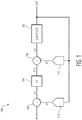
- FIG. 1 illustrates, in simplified block diagram form, an example sigma-delta modulator 100 in accordance with an embodiment.
- Modulator 100 includes an input labeled IN for receiving a differential input signal and an output labeled OUT for providing a digital differential output signal corresponding to the sampled analog signal.
- modulator 100 includes summing circuits 102 and 106, a loop filter circuit (LF) 104, a quantizer circuit 108, and digital-to-analog converter (DAC) circuits 110 and 112.
- quantizer 108 may be implemented as a single-bit quantizer and thus referred to as a comparator coupled to a memory element.
- the memory element is configured and arranged for storing output data of the comparator which may be subsequently processed by DAC circuits 110 and 112.
- First summing circuit 102 includes a first input coupled to receive the analog signal (e.g., differential signal) and an output coupled to an input of loop filter 104 at node labeled D1.
- An output of loop filter 104 is coupled to a first input of second summing circuit 106 at node labeled FD1 and an output of second summing circuit 106 is coupled to an input of quantizer 108 at node labeled D2.
- An output of quantizer 108 is coupled to inputs of DACs 110 and 112 and provides the OUT digital value corresponding to the sampled analog signal.
- An output of DAC 110 is coupled to a second input of summing circuit 102 at node A1 and an output of DAC 112 is coupled to a second input of summing circuit 106 at node A2.
- a first feedback loop includes DAC 110 and summing circuit 102 and a second feedback loop includes DAC 112 and summing circuit 106.
- summing circuit 102 generates a first difference signal D1 by subtracting an analog output signal A1 of DAC 110 from the analog input signal IN.
- the analog signal A1 corresponds to the digital value OUT received at the DAC 110 input.
- Loop filter 104 generates a filtered signal FD1 based on the received first difference signal D1.
- Summing circuit 106 generates a second difference signal D2 by subtracting an analog output signal A2 of DAC 112 from the received signal FD1.
- the analog signal A2 corresponds to the digital value OUT received at the DAC 112 input.
- DAC 112 is included to form as an excess loop (ELD) compensation path to further stabilize the overall feedback loop.
- Quantizer 108 generates the digital value OUT based on the received signal D2.
- the digital value OUT includes a complementary digital signal pair, each signal of the pair may be any of a logic high (e.g., logic one) and a logic low (e.g., logic zero), and DACs 110 and 112 may be characterized as one-bit DACs.
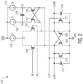
- FIG. 2 illustrates, in simplified schematic diagram form, an example implementation of comparator 200 included in the quantizer 108 of modulator 100 in accordance with an embodiment.
- comparator 200 may be characterized as a differential single-bit comparator having an integrated latch circuit (e.g., memory element).
- Comparator 200 includes inputs labeled VP and VN for receiving a differential signal, an input labeled CLK for receiving a control clock signal, a first output labeled OUTP for providing a digital signal corresponding to the received differential signal, and a second output labeled OUTN for providing a complementary (e.g., inverse) digital signal corresponding to the received differential signal.
- comparator 200 includes an amplifier portion formed by P-channel transistors 202-204 and current source 218, a latch and reset portion formed by N-channel transistors 206-212, and negative capacitance portion formed by P-channel transistors 224-226, capacitor 228, and current sources 220-222.
- Capacitors 214-216 represent parasitic capacitances coupled at OUTN and OUTP outputs.
- the amplifier portion includes transistors 202-204 and current source 218.
- the amplifier portion is coupled to receive the differential signal at control electrodes of transistor 202 and transistor 204 respectively.
- a first current electrode of transistor 202 is coupled to a first current electrode of transistor 204 and a first terminal of current source 218 at node labeled N1.
- a second current electrode of transistor 202 is coupled at output OUTN and a second current electrode of transistor 204 is coupled at output OUTP.
- a second terminal of current source 218 is coupled to a first voltage supply terminal labeled VDD.
- current source 218 is configured to provide a current I1.
- a normal operating voltage is supplied at the VDD supply terminal, and transistors 202 and 204 are formed to have substantially similar size parameters (e.g., width and length values) as each other.
- the latch and reset portion includes transistors 206-212 and is coupled to the amplifier portion at OUTN and OUTP outputs.
- transistors 206 and 208 are cross-coupled and configured to form a latching circuit with transistors 206 and 208 having substantially similar size parameters as each other.
- a first current electrode of transistor 206 is coupled at output OUTN
- a control electrode of transistor 206 is coupled at output OUTP
- a second current electrode of transistor 206 is coupled to a second voltage supply terminal labeled GND.
- a ground voltage e.g., 0 volts
- a first current electrode of transistor 208 is coupled at output OUTP
- a control electrode of transistor 208 is coupled at output OUTN
- a second current electrode of transistor 208 is coupled at the GND supply terminal.
- Transistors 210 and 212 are configured to form a reset circuit such that a first state (e.g., logic high) of the CLK control signal causes the latching circuit to reset in this embodiment.
- a first current electrode of transistor 210 is coupled at output OUTN, a control electrode of transistor 210 is coupled to receive the CLK control signal, and a second current electrode of transistor 210 is coupled at the GND supply terminal.
- a first current electrode of transistor 212 is coupled at output OUTP, a control electrode of transistor 212 is coupled to receive the CLK control signal, and a second current electrode of transistor 212 is coupled at the GND supply terminal.
- the reset circuit when the CLK control signal is at a second state (e.g., logic low), the reset circuit is inactive allowing the latching circuit to sense a voltage difference (e.g., across outputs OUTN and OUTP) and latch accordingly.
- a voltage difference e.g., across outputs OUTN and OUTP
- Capacitors 214 and 216 depicting parasitic capacitances coupled at OUTN and OUTP outputs are shown for illustrative purposes.
- a first terminal of capacitor 214 is coupled at output OUTN
- a first terminal of capacitor 216 is coupled at output OUTP
- second terminals of capacitors 214 and 216 are coupled at the GND supply terminal.
- capacitors 214 and 216 have substantially similar capacitance values as each other.
- the negative capacitance portion is coupled to the amplifier portion and the latch portion at outputs OUTN and OUTP.
- the negative capacitance portion is configured to substantially cancel the parasitic capacitance coupled at output OUTN and output OUTP.
- the negative capacitance portion includes transistors 224 and 226, capacitor 228, and current sources 220 and 222.
- transistors 224 and 226 are configured in a cross-coupled arrangement where transistors 224 and 226 have substantially similar size parameters as each other.
- a first current electrode of transistor 224 is coupled at output OUTP
- a control electrode of transistor 224 is coupled at output OUTN
- a second current electrode of transistor 224 is coupled to a first terminal of capacitor 228 and a first terminal of current source 220 at node labeled N2.
- a first current electrode of transistor 226 is coupled at output OUTN, a control electrode of transistor 226 is coupled at output OUTP, and a second current electrode of transistor 226 is coupled to a second terminal of capacitor 228 and a first terminal of current source 222 at node labeled N3.
- a second terminal of current source 220 and a second terminal of current source 222 are coupled at the VDD supply terminal.
- current source 220 is configured to provide a current 12 substantially one-half of current I1
- current source 222 is configured to provide a current 13 substantially equal to current I2.
- capacitor 228 is configured to have a capacitance substantially equal to the parasitic capacitance coupled at each of outputs OUTN and OUTP.
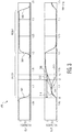
- FIG. 3 illustrates, in plot diagram form, an example simulation result of the comparator 200 included in quantizer 108 of modulator 100 in accordance with an embodiment.
- the plot diagram 300 includes CLK control signal timing and corresponding differential output signal OUT (e.g., OUTN and OUTP) simulation response waveforms.
- the CLK and OUT waveforms are shown with time values in nanoseconds (ns) on the X-axis and voltage values in volts (V) on the Y-axes.
- the CLK waveform includes signal transitions 302-306 which delineate the operational phases (e.g., LATCH and RESET) of quantizer 108.
- the OUT waveform includes a first differential waveform formed by signals 308 and 310 and a second differential waveform formed by (dashed) signals 312 and 314 depicting simulation results of comparator 200 during normal operation.
- the first differential waveform depicts a first simulation result of comparator 200 without using of the negative capacitance circuitry and the second differential waveform depicts a second simulation result overlaying the first simulation result of comparator 200 showing a desired access time improvement by utilizing the negative capacitance circuitry.
- the comparator 200 enters a LATCH phase as the CLK control signal transitions (302) from a logic high to a logic low.
- a voltage difference across the differential inputs (e.g., VP, VN) of comparator 200 causes the latching portion to start latching.
- signals 312 and 314 of the second differential waveform have reached predetermined thresholds indicative of respective logic high and logic low values.
- Arrow 318 indicates an access time from time t1 to time t2 for the comparator 200 utilizing the negative capacitance circuitry.
- signals 308 and 310 of the first differential waveform have reached the predetermined thresholds indicative of respective logic high and logic low values.
- Arrow 316 indicates an access time from time t1 to time t3 for the comparator 200 without using the negative capacitance circuitry.
- the access time of the comparator 200 utilizing the negative capacitance circuitry is significantly shorter (e.g., ⁇ 20%). By having a shorter access time, the comparator 200 can operate at significantly higher frequencies.
- the LATCH phase ends and the RESET phase begins as the CLK control signal transitions (304) from the logic low to a logic high at approximately 1.2 ns in this example.
- the comparator 200 enters the LATCH phase again as the CLK control signal transitions (306) to a logic low.
- the CLK control signal is illustrated as a 50% duty cycle signal. In some embodiments, the CLK control signal may be configured having a less than 50% duty cycle, and in other embodiments, the CLK control signal may be configured having a greater than 50% duty cycle.
- a circuit including an amplifier portion having a first input coupled to receive a first analog signal and a first output; a latch portion coupled to the amplifier portion, the latch portion configured to provide at the first output a digital value based on the first analog signal; and a negative capacitance portion coupled to the first output, the negative capacitance portion configured to cancel parasitic capacitance coupled at the first output.
- the negative capacitance portion may further include a first transistor having a first current electrode coupled to the first output, a second transistor having a first current electrode coupled to a control electrode of the first transistor and a control electrode coupled to the first output, and a capacitor having a first terminal coupled to a second current electrode of the first transistor and a second terminal coupled to a second current electrode of the second transistor.
- the capacitor may have a capacitance value substantially equal to the parasitic capacitance coupled at the first output.
- the negative capacitance portion may further include a first current source having a first terminal coupled to a first voltage supply terminal and a second terminal coupled to the second current electrode of the first transistor, and a second current source having a first terminal coupled to the first voltage supply terminal and a second terminal coupled to the second current electrode of the second transistor.
- the amplifier portion may further include a first transistor having a first current electrode, a second current electrode coupled to a second output, and a control electrode coupled to receive the first analog signal, and a second transistor having a first current electrode coupled to the first current electrode of the first transistor, a second current electrode coupled to the first output, and a control electrode coupled to receive a second analog signal, the first analog signal and the second analog signal together comprising a differential signal.
- the amplifier portion may further include a first current source having a first terminal coupled to a first voltage supply terminal and a second terminal coupled to the first current electrodes of the first and second transistors.
- the latch portion may further include a third transistor having a first current electrode coupled to the second current electrode of the first transistor at the second output, a second current electrode coupled to a second voltage supply terminal, and a control electrode coupled to the second current electrode of the second transistor at the first output, and a fourth transistor having a first current electrode coupled to the second current electrode of the second transistor, a second current electrode couple to the second voltage supply terminal, and a control electrode coupled to the second current electrode of the first transistor.
- the circuit may further include a first digital-to-analog converter (DAC) having an input coupled to the first output, an output of the DAC coupled to provide a second analog signal representative of the digital value.
- the circuit may further include a summing circuit having a first input coupled to receive an input signal, a second input for receiving the second analog signal, and an output coupled to provide a first difference signal generated by subtracting the second analog signal from the input signal.
- a circuit including an amplifier portion having a first input coupled to receive a first analog signal and a first output, the amplifier portion coupled between a first voltage supply terminal and the first output; a latch portion coupled to the amplifier portion at the first output, the latch portion configured to provide a digital value based on the first analog signal; and a negative capacitance portion coupled to the amplifier portion and the latch portion at the first output, the negative capacitance portion configured to cancel parasitic capacitance coupled at the first output.
- the negative capacitance portion may further include a first transistor coupled between the first voltage supply terminal and the first output, the first transistor having a first current electrode coupled to the first output, a second transistor having a first current electrode coupled to a control electrode of the first transistor and a control electrode coupled to the first current electrode of the first transistor, and a capacitor having a first terminal coupled to a second current electrode of the first transistor and a second terminal coupled to a second current electrode of the second transistor, the capacitor having a capacitance value substantially equal to the parasitic capacitance coupled at the first output.
- the negative capacitance portion may further include a first current source having a first terminal coupled to the first voltage supply terminal and a second terminal coupled to the second current electrode of the first transistor, and a second current source having a first terminal coupled to the first voltage supply terminal and a second terminal coupled to the second current electrode of the second transistor.
- the amplifier portion may further include a third current source coupled to the first voltage supply terminal, a third transistor having a first current electrode coupled to the third current source and a control electrode coupled to receive the first analog signal, and a fourth transistor having a first current electrode coupled to the first current source, a second current electrode coupled to the first output, and a control electrode coupled to receive a second analog signal, the first analog signal and the second analog signal together comprising a differential signal.
- the third current source may be configured to source an amount of current substantially equal to the sum of current sourced by the first current source and the second current source.
- the circuit may further include a first digital-to-analog converter (DAC) having an input coupled to the first output, an output of the DAC coupled to provide a second analog signal representative of the digital value.
- the circuit may further include a summing circuit having a first input coupled to receive an input signal, a second input for receiving the second analog signal, and an output coupled to the first input of the amplifier portion. The summing circuit may be configured to provide at the output a first difference signal generated by subtracting the second analog signal from the input signal.
- a circuit including an amplifier portion including: a first transistor having a first current electrode, a second current electrode coupled to a first output, and a control electrode coupled to receive a first analog signal, and a second transistor having a first current electrode coupled to the first current electrode of the first transistor, a second current electrode coupled to a second output, and a control electrode coupled to receive a second analog signal, the first analog signal and the second analog signal together comprising a differential signal; a latch portion coupled to the amplifier portion, the latch portion including: a third transistor having a first current electrode coupled at the second output and a control electrode coupled at the first output, and a fourth transistor having a first current electrode coupled at the first output and a control electrode coupled at the second output; and a negative capacitance portion coupled to the amplifier portion and the latch portion, the negative capacitance portion including: a fifth transistor having a first current electrode coupled at the first output and a control electrode coupled at the second output, a sixth transistor having a first current electrode coupled at the second output
- the capacitor may have a capacitance value substantially equal to parasitic capacitance coupled at the first output or the second output.
- the circuit may further include a seventh transistor having a first current electrode coupled at the second output and a control electrode coupled to receive a control signal, and an eighth transistor having a first current electrode coupled at the first output and a control electrode coupled to receive the control signal, wherein the control signal at first logic state causes the seventh and eighth transistors to conduct and resets the latch portion.
- a quantizer configured to cancel output parasitic capacitance.
- negative capacitance circuitry to cancel the output parasitic capacitance of the quantizer.
- the quantizer can be configured to operate at higher frequencies. Greater throughput can be achieved by processing samples with the quantizer operating at higher frequencies.
- a high-speed comparator circuit includes an amplifier portion, a latch portion, and a negative capacitance portion.
- the amplifier portion includes an input coupled to receive an analog signal and an output.
- the latch portion is coupled to the amplifier portion.
- the latch portion is configured to provide at the output a digital value based on the analog signal.
- the negative capacitance portion is coupled to the output.
- the negative capacitance portion is configured to cancel parasitic capacitance coupled at the first output.
- Coupled is not intended to be limited to a direct coupling or a mechanical coupling.
Landscapes
- Engineering & Computer Science (AREA)
- Power Engineering (AREA)
- Theoretical Computer Science (AREA)
- Analogue/Digital Conversion (AREA)
Applications Claiming Priority (1)
| Application Number | Priority Date | Filing Date | Title |
|---|---|---|---|
| US16/455,992 US11716074B2 (en) | 2019-06-28 | 2019-06-28 | Comparator with negative capacitance compensation |
Publications (1)
| Publication Number | Publication Date |
|---|---|
| EP3758221A1 true EP3758221A1 (de) | 2020-12-30 |
Family
ID=71120099
Family Applications (1)
| Application Number | Title | Priority Date | Filing Date |
|---|---|---|---|
| EP20181405.0A Ceased EP3758221A1 (de) | 2019-06-28 | 2020-06-22 | Komparator mit negativer kapazitätskompensation |
Country Status (3)
| Country | Link |
|---|---|
| US (1) | US11716074B2 (de) |
| EP (1) | EP3758221A1 (de) |
| CN (1) | CN112152628B (de) |
Families Citing this family (3)
| Publication number | Priority date | Publication date | Assignee | Title |
|---|---|---|---|---|
| TWI761263B (zh) * | 2021-07-15 | 2022-04-11 | 瑞昱半導體股份有限公司 | 合成負阻抗的電路 |
| CN113872574A (zh) * | 2021-09-29 | 2021-12-31 | 南京邮电大学 | 一种应用于高速模数转换器的高速比较器 |
| US20260066919A1 (en) * | 2024-09-04 | 2026-03-05 | Nxp B.V. | High-Speed Continuous-Time Delta-Sigma Modulator Including an Amplifier with Limited Gain |
Citations (1)
| Publication number | Priority date | Publication date | Assignee | Title |
|---|---|---|---|---|
| US9264056B2 (en) * | 2012-09-03 | 2016-02-16 | Tensorcom, Inc. | Method and apparatus for an active negative-capacitor circuit to cancel the input capacitance of comparators |
Family Cites Families (8)
| Publication number | Priority date | Publication date | Assignee | Title |
|---|---|---|---|---|
| JP4866482B2 (ja) * | 2007-08-10 | 2012-02-01 | ナショナル ユニヴァーシティー オブ シンガポール | 帯域通過シグマ−デルタ変調のためのシステム及び方法 |
| US8228120B2 (en) * | 2009-05-29 | 2012-07-24 | Intersil Americas Inc. | Negative capacitance synthesis for use with differential circuits |
| US9184957B2 (en) * | 2012-12-27 | 2015-11-10 | Intel Corporation | High speed receivers circuits and methods |
| US8872587B2 (en) * | 2013-03-06 | 2014-10-28 | International Business Machines Corporation | Generating negative impedance compensation |
| US9350331B2 (en) * | 2013-03-14 | 2016-05-24 | Marvell World Trade Ltd. | High speed latch with over voltage protection and integrated summing nodes |
| US8884655B2 (en) * | 2013-04-11 | 2014-11-11 | Texas Instruments Incorporated | Low-power voltage mode high speed driver |
| US9490832B1 (en) * | 2015-11-16 | 2016-11-08 | Xilinx, Inc. | Analog-to-digital converter circuit and method of implementing an analog-to-digital converter circuit |
| EP3413468A1 (de) * | 2017-06-08 | 2018-12-12 | Nxp B.V. | Sigma-delta-modulator, integrierte schaltung und verfahren dafür |
-
2019
- 2019-06-28 US US16/455,992 patent/US11716074B2/en active Active
-
2020
- 2020-06-18 CN CN202010562731.0A patent/CN112152628B/zh active Active
- 2020-06-22 EP EP20181405.0A patent/EP3758221A1/de not_active Ceased
Patent Citations (1)
| Publication number | Priority date | Publication date | Assignee | Title |
|---|---|---|---|---|
| US9264056B2 (en) * | 2012-09-03 | 2016-02-16 | Tensorcom, Inc. | Method and apparatus for an active negative-capacitor circuit to cancel the input capacitance of comparators |
Non-Patent Citations (3)
| Title |
|---|
| BEHZAD RAZAVI: "Design of Integrated Circuits for Optical Communications Second Edition", 21 August 2012 (2012-08-21), pages 174 - 179, XP055745084, Retrieved from the Internet <URL:https://www.wiley.com/en-us/Design+of+Integrated+Circuits+for+Optical+Communications%2C+2nd+Edition-p-9781118439456> [retrieved on 20201029] * |
| BOSKO MRKOVIC ET AL: "The simple CMOS negative capacitance with improved frequency response", MIPRO, 2012 PROCEEDINGS OF THE 35TH INTERNATIONAL CONVENTION, IEEE, 21 May 2012 (2012-05-21), pages 87 - 90, XP032201887, ISBN: 978-1-4673-2577-6 * |
| MURATORE DANTE GABRIEL ET AL: "Very high-speed CMOS comparators for multi-GS/s A/D converters", 2015 11TH CONFERENCE ON PH.D. RESEARCH IN MICROELECTRONICS AND ELECTRONICS (PRIME), IEEE, 29 June 2015 (2015-06-29), pages 240 - 243, XP033200795, DOI: 10.1109/PRIME.2015.7251379 * |
Also Published As
| Publication number | Publication date |
|---|---|
| US20200412345A1 (en) | 2020-12-31 |
| US11716074B2 (en) | 2023-08-01 |
| CN112152628B (zh) | 2025-10-28 |
| CN112152628A (zh) | 2020-12-29 |
Similar Documents
| Publication | Publication Date | Title |
|---|---|---|
| US7405682B2 (en) | Delta-sigma analog digital converter with offset compensation | |
| JP3039809B2 (ja) | アナログ/ディジタル変換器、サンプリングパルス生成回路、及び電流スイッチ回路 | |
| US5691720A (en) | Delta sigma analog-to-digital converter having programmable resolution/bias current circuitry and method | |
| US8198921B2 (en) | Dynamic comparator with background offset calibration | |
| CN113131882B (zh) | 放大器、电路及处理信号的方法 | |
| EP3758221A1 (de) | Komparator mit negativer kapazitätskompensation | |
| CN110235372B (zh) | 一种具有降低回扫噪声的双倍数据速率时间内插量化器 | |
| US9438262B1 (en) | Method for testing differential analog-to-digital converter and system therefor | |
| US10554218B1 (en) | Sigma-delta modulator | |
| EP2521269A1 (de) | Sigma-delta-modulator | |
| CN113271103A (zh) | 电阻式高速高精度sar-adc/dac电路及无线充电设备 | |
| EP3931969B1 (de) | Analog-digital-wandlerschaltung | |
| US10305452B2 (en) | Five-level switched-capacitance DAC using bootstrapped switches | |
| US20250055421A1 (en) | Nested floating-inverter based amplifier | |
| Pelgrom | Nyquist analog-to-digital conversion | |
| US20110234290A1 (en) | Switched-capacitor current reference with reduced output ripple | |
| CN116032217A (zh) | 振荡器结构及包括振荡器结构的模数转换系统 | |
| US20250119152A1 (en) | Semiconductor device | |
| US11652470B2 (en) | Phase rotator control apparatus and method therefor | |
| Huang et al. | A 1.2 V direct background digital tuned continuous-time bandpass sigma-delta modulator | |
| US12418307B2 (en) | Return to open DAC with resistor bypass on reset | |
| Sung et al. | A comparison of second-order sigma-delta modulator between switched-capacitor and switched-current techniques | |
| US11646662B2 (en) | Reference buffer | |
| George et al. | A 94-dB SFDR multi-bit audio-band delta-sigma converter with DAC nonlinearity suppression | |
| Katara et al. | Development of one bit delta-sigma analog to digital converter |
Legal Events
| Date | Code | Title | Description |
|---|---|---|---|
| PUAI | Public reference made under article 153(3) epc to a published international application that has entered the european phase |
Free format text: ORIGINAL CODE: 0009012 |
|
| STAA | Information on the status of an ep patent application or granted ep patent |
Free format text: STATUS: THE APPLICATION HAS BEEN PUBLISHED |
|
| AK | Designated contracting states |
Kind code of ref document: A1 Designated state(s): AL AT BE BG CH CY CZ DE DK EE ES FI FR GB GR HR HU IE IS IT LI LT LU LV MC MK MT NL NO PL PT RO RS SE SI SK SM TR |
|
| AX | Request for extension of the european patent |
Extension state: BA ME |
|
| STAA | Information on the status of an ep patent application or granted ep patent |
Free format text: STATUS: REQUEST FOR EXAMINATION WAS MADE |
|
| 17P | Request for examination filed |
Effective date: 20210630 |
|
| RBV | Designated contracting states (corrected) |
Designated state(s): AL AT BE BG CH CY CZ DE DK EE ES FI FR GB GR HR HU IE IS IT LI LT LU LV MC MK MT NL NO PL PT RO RS SE SI SK SM TR |
|
| STAA | Information on the status of an ep patent application or granted ep patent |
Free format text: STATUS: THE APPLICATION HAS BEEN REFUSED |
|
| 18R | Application refused |
Effective date: 20230209 |