EP3760765B1 - Système de croissance horizontale de monocristaux à semiconducteur de haute qualité et son procédé de fabrication - Google Patents
Système de croissance horizontale de monocristaux à semiconducteur de haute qualité et son procédé de fabrication Download PDFInfo
- Publication number
- EP3760765B1 EP3760765B1 EP19184259.0A EP19184259A EP3760765B1 EP 3760765 B1 EP3760765 B1 EP 3760765B1 EP 19184259 A EP19184259 A EP 19184259A EP 3760765 B1 EP3760765 B1 EP 3760765B1
- Authority
- EP
- European Patent Office
- Prior art keywords
- growth
- pvt
- reactor
- pvt growth
- semiconductor single
- Prior art date
- Legal status (The legal status is an assumption and is not a legal conclusion. Google has not performed a legal analysis and makes no representation as to the accuracy of the status listed.)
- Active
Links
Images





Classifications
-
- C—CHEMISTRY; METALLURGY
- C30—CRYSTAL GROWTH
- C30B—SINGLE-CRYSTAL GROWTH; UNIDIRECTIONAL SOLIDIFICATION OF EUTECTIC MATERIAL OR UNIDIRECTIONAL DEMIXING OF EUTECTOID MATERIAL; REFINING BY ZONE-MELTING OF MATERIAL; PRODUCTION OF A HOMOGENEOUS POLYCRYSTALLINE MATERIAL WITH DEFINED STRUCTURE; SINGLE CRYSTALS OR HOMOGENEOUS POLYCRYSTALLINE MATERIAL WITH DEFINED STRUCTURE; AFTER-TREATMENT OF SINGLE CRYSTALS OR A HOMOGENEOUS POLYCRYSTALLINE MATERIAL WITH DEFINED STRUCTURE; APPARATUS THEREFOR
- C30B23/00—Single-crystal growth by condensing evaporated or sublimed materials
- C30B23/002—Controlling or regulating
- C30B23/005—Controlling or regulating flux or flow of depositing species or vapour
-
- C—CHEMISTRY; METALLURGY
- C30—CRYSTAL GROWTH
- C30B—SINGLE-CRYSTAL GROWTH; UNIDIRECTIONAL SOLIDIFICATION OF EUTECTIC MATERIAL OR UNIDIRECTIONAL DEMIXING OF EUTECTOID MATERIAL; REFINING BY ZONE-MELTING OF MATERIAL; PRODUCTION OF A HOMOGENEOUS POLYCRYSTALLINE MATERIAL WITH DEFINED STRUCTURE; SINGLE CRYSTALS OR HOMOGENEOUS POLYCRYSTALLINE MATERIAL WITH DEFINED STRUCTURE; AFTER-TREATMENT OF SINGLE CRYSTALS OR A HOMOGENEOUS POLYCRYSTALLINE MATERIAL WITH DEFINED STRUCTURE; APPARATUS THEREFOR
- C30B25/00—Single-crystal growth by chemical reaction of reactive gases, e.g. chemical vapour-deposition growth
- C30B25/02—Epitaxial-layer growth
- C30B25/16—Controlling or regulating
-
- C—CHEMISTRY; METALLURGY
- C30—CRYSTAL GROWTH
- C30B—SINGLE-CRYSTAL GROWTH; UNIDIRECTIONAL SOLIDIFICATION OF EUTECTIC MATERIAL OR UNIDIRECTIONAL DEMIXING OF EUTECTOID MATERIAL; REFINING BY ZONE-MELTING OF MATERIAL; PRODUCTION OF A HOMOGENEOUS POLYCRYSTALLINE MATERIAL WITH DEFINED STRUCTURE; SINGLE CRYSTALS OR HOMOGENEOUS POLYCRYSTALLINE MATERIAL WITH DEFINED STRUCTURE; AFTER-TREATMENT OF SINGLE CRYSTALS OR A HOMOGENEOUS POLYCRYSTALLINE MATERIAL WITH DEFINED STRUCTURE; APPARATUS THEREFOR
- C30B23/00—Single-crystal growth by condensing evaporated or sublimed materials
- C30B23/02—Epitaxial-layer growth
-
- C—CHEMISTRY; METALLURGY
- C30—CRYSTAL GROWTH
- C30B—SINGLE-CRYSTAL GROWTH; UNIDIRECTIONAL SOLIDIFICATION OF EUTECTIC MATERIAL OR UNIDIRECTIONAL DEMIXING OF EUTECTOID MATERIAL; REFINING BY ZONE-MELTING OF MATERIAL; PRODUCTION OF A HOMOGENEOUS POLYCRYSTALLINE MATERIAL WITH DEFINED STRUCTURE; SINGLE CRYSTALS OR HOMOGENEOUS POLYCRYSTALLINE MATERIAL WITH DEFINED STRUCTURE; AFTER-TREATMENT OF SINGLE CRYSTALS OR A HOMOGENEOUS POLYCRYSTALLINE MATERIAL WITH DEFINED STRUCTURE; APPARATUS THEREFOR
- C30B23/00—Single-crystal growth by condensing evaporated or sublimed materials
- C30B23/02—Epitaxial-layer growth
- C30B23/06—Heating of the deposition chamber, the substrate or the materials to be evaporated
-
- C—CHEMISTRY; METALLURGY
- C30—CRYSTAL GROWTH
- C30B—SINGLE-CRYSTAL GROWTH; UNIDIRECTIONAL SOLIDIFICATION OF EUTECTIC MATERIAL OR UNIDIRECTIONAL DEMIXING OF EUTECTOID MATERIAL; REFINING BY ZONE-MELTING OF MATERIAL; PRODUCTION OF A HOMOGENEOUS POLYCRYSTALLINE MATERIAL WITH DEFINED STRUCTURE; SINGLE CRYSTALS OR HOMOGENEOUS POLYCRYSTALLINE MATERIAL WITH DEFINED STRUCTURE; AFTER-TREATMENT OF SINGLE CRYSTALS OR A HOMOGENEOUS POLYCRYSTALLINE MATERIAL WITH DEFINED STRUCTURE; APPARATUS THEREFOR
- C30B25/00—Single-crystal growth by chemical reaction of reactive gases, e.g. chemical vapour-deposition growth
- C30B25/02—Epitaxial-layer growth
- C30B25/08—Reaction chambers; Selection of materials therefor
-
- C—CHEMISTRY; METALLURGY
- C30—CRYSTAL GROWTH
- C30B—SINGLE-CRYSTAL GROWTH; UNIDIRECTIONAL SOLIDIFICATION OF EUTECTIC MATERIAL OR UNIDIRECTIONAL DEMIXING OF EUTECTOID MATERIAL; REFINING BY ZONE-MELTING OF MATERIAL; PRODUCTION OF A HOMOGENEOUS POLYCRYSTALLINE MATERIAL WITH DEFINED STRUCTURE; SINGLE CRYSTALS OR HOMOGENEOUS POLYCRYSTALLINE MATERIAL WITH DEFINED STRUCTURE; AFTER-TREATMENT OF SINGLE CRYSTALS OR A HOMOGENEOUS POLYCRYSTALLINE MATERIAL WITH DEFINED STRUCTURE; APPARATUS THEREFOR
- C30B29/00—Single crystals or homogeneous polycrystalline material with defined structure characterised by the material or by their shape
- C30B29/10—Inorganic compounds or compositions
- C30B29/36—Carbides
-
- C—CHEMISTRY; METALLURGY
- C30—CRYSTAL GROWTH
- C30B—SINGLE-CRYSTAL GROWTH; UNIDIRECTIONAL SOLIDIFICATION OF EUTECTIC MATERIAL OR UNIDIRECTIONAL DEMIXING OF EUTECTOID MATERIAL; REFINING BY ZONE-MELTING OF MATERIAL; PRODUCTION OF A HOMOGENEOUS POLYCRYSTALLINE MATERIAL WITH DEFINED STRUCTURE; SINGLE CRYSTALS OR HOMOGENEOUS POLYCRYSTALLINE MATERIAL WITH DEFINED STRUCTURE; AFTER-TREATMENT OF SINGLE CRYSTALS OR A HOMOGENEOUS POLYCRYSTALLINE MATERIAL WITH DEFINED STRUCTURE; APPARATUS THEREFOR
- C30B35/00—Apparatus not otherwise provided for, specially adapted for the growth, production or after-treatment of single crystals or of a homogeneous polycrystalline material with defined structure
- C30B35/002—Crucibles or containers
-
- C—CHEMISTRY; METALLURGY
- C30—CRYSTAL GROWTH
- C30B—SINGLE-CRYSTAL GROWTH; UNIDIRECTIONAL SOLIDIFICATION OF EUTECTIC MATERIAL OR UNIDIRECTIONAL DEMIXING OF EUTECTOID MATERIAL; REFINING BY ZONE-MELTING OF MATERIAL; PRODUCTION OF A HOMOGENEOUS POLYCRYSTALLINE MATERIAL WITH DEFINED STRUCTURE; SINGLE CRYSTALS OR HOMOGENEOUS POLYCRYSTALLINE MATERIAL WITH DEFINED STRUCTURE; AFTER-TREATMENT OF SINGLE CRYSTALS OR A HOMOGENEOUS POLYCRYSTALLINE MATERIAL WITH DEFINED STRUCTURE; APPARATUS THEREFOR
- C30B29/00—Single crystals or homogeneous polycrystalline material with defined structure characterised by the material or by their shape
- C30B29/10—Inorganic compounds or compositions
- C30B29/40—AIIIBV compounds wherein A is B, Al, Ga, In or Tl and B is N, P, As, Sb or Bi
Definitions
- the present invention relates to systems and methods for growing high-quality bulk semiconductor single crystals , and more specifically, for horizontal growth of semiconductor single crystals, such as silicon carbide, in a horizontal direction with respect to the direction of gravity based on physical vapor transport.
- Silicon carbide is extensively used as a semiconductor substrate material for electronic components in a wide range of applications, such as power electronics, radio frequency and light emitting semiconductors components.
- SiC substrates are then produced from the single crystal boule by cutting slices or wafers from the bulk SiC crystal (for e.g. using wire saws) and finishing the substrate surface with a sequence of polishing steps.
- the finished SiC substrates are employed in the manufacturing of semiconductor components, such as in epitaxial processes where thin monocrystalline layers of a suitable semiconductor material (e.g., SiC, GaN) are deposited onto the SiC substrate.
- a suitable semiconductor material e.g., SiC, GaN
- PVT is a crystal growing method that essentially involves sublimation of a suitable source material followed by re-condensation at a seed crystal, where the formation of the single crystal takes place.
- the source material and seed crystal are placed inside a growth structure, where the source material is sublimed by heating.
- the sublimed vapor then diffuses towards the seed in a controlled manner, due to a temperature gradient established between source material and seed crystal, and deposits onto the seed where it grows as a single crystal.
- the core of the PVT-based growth system is the so-called reactor, which provides a chamber where the growth structure is placed and a low-pressure atmosphere suitable for the growth of the single crystal is created.
- the inner walls of the growth structure are in general made of a porous graphite with density of, for example at least 1.75 g/cm 3 , through which doping components in gaseous form or inert gases may penetrate into the growth compartment by porosity.
- Heat for subliming the source material inside the PVT growth structures is generally provided by either inductive or resistive heating systems. The temperature within the growth structure is measured by one or more pyrometers or thermocouples installed close to an overture of the growth structure.
- the vacuum-sealed reactor is evacuated by one or more vacuum pumps and supplied with inert or doping gases via one or more gas feeds to create a controlled gas (gas mixture atmosphere). All process parameters (pressure, temperature, gas flow, etc.) can be adjusted, controlled and stored by a computer-operated system controller, which communicates with all involved components (for e.g. inverter, pyrometer, vacuum control valve, MFC, and pressure gauges, as described with more detail below with reference to Fig. 3 ).
- a computer-operated system controller which communicates with all involved components (for e.g. inverter, pyrometer, vacuum control valve, MFC, and pressure gauges, as described with more detail below with reference to Fig. 3 ).
- the reactor usually includes one or more glass tubes, which are optionally cooled with water and provided at both ends with flanges to complete the interior of the reactor against the atmosphere.
- An example of such an inductively heated PVT system is described in patent US 8,865,324 B2 .
- the heating induction coil is mounted outside the reactor and usually surrounded by a "Faraday cage” that provides a shield from electromagnetic radiation.
- the heating resistive elements are mounted inside the reactor.
- the reactor is made of metal, it can be cooled by water or air. Examples of resistively-heated PVT systems are described in published patent applications US 2016/0138185 and US 2017/0321345 .
- Such PVT growth systems known in the art are vertically oriented, i.e. both the reactor and the PVT growth structure arranged inside are oriented with the respective longitudinal axis, which essentially correspond to the growth direction of the single crystal(s), parallel to the gravity direction.
- the vertical orientation is in general used because the graphite/carbon materials forming the inner walls of the PVT growth structure are attacked by the components of the sublimed source material (for e.g. Si-containing gaseous species) and the high temperatures reached during the growth process.
- the subsequent degradation of the graphite/carbon material results in graphite particles being detached from the inner walls and released into the crystal growth compartment, which then fall towards the PVT growth structure lower side under the effect of gravity.
- the crystal boule grows on an upper side of the PVT growth structure so that the released graphite/carbon particles do not come into contact with the growing crystal.
- high-quality single crystals can still be produced in conventional vertical PVT growth systems since the single crystal boule growing on the upper side of the PVT growth structure is not contaminated by graphite particles released during the growth process.
- Fig. 1 illustrates an exemplary growth structure 100 for producing one single crystal boule in a vertical orientation, as commonly employed in conventional PVT growth systems.
- the vertical direction is represented in Fig. 1 by an arrow indicating the direction of the gravity force vector F g .
- the PVT growth structure 100 has a crucible 102 where a source material compartment 104 with a source material 106 (for e.g. SiC in powder or granular form) is provided on a lower side (with respect to gravity) and a seed crystal 108 is arranged in a growth compartment 110 on an upper side and at a certain distance, along a longitudinal axis 116, from the source material compartment 106.
- a source material compartment 104 with a source material 106 for e.g. SiC in powder or granular form
- the PVT growth structure 100 may also include thermal insulation 114 surrounding the crucible 102.
- the thermal insulation 114 is in general made of a porous, thermal insulating material, such as foam-like graphite, with a porosity higher than that of the crucible graphite material itself.
- the single crystal boule 109 grows onto the crystal seed 108 along the longitudinal axis 116, which is in general aligned in the direction of the gravity force ( F g ), and on the upper side of the crucible 102 so that the single crystal boule 109 is not contaminated by graphite particles during crystal growth.
- Patent application publication EP 2 664 695 describes a process that allows manufacturing two single crystals within a same vertical PVT growth structure in simultaneous.
- a single crystal is grown at a top side of the PVT growth structure, which is vertically arranged inside a vertical reactor, such as described in the prior art, and a second crystal is simultaneously grown on a bottom side of the PVT growth structure.
- graphite/carbon particles released from the inner walls of the PVT growth structure may still fall onto the crystal boule growing on a lower side of the PVT growth structure, thereby forming graphite/carbon inclusions inside the crystal during the growth process that significantly reduce crystal quality.
- Graphite/carbon inclusions also reduce the yield of high-quality substrates and wafers, and therefore, results in undesirable rejections and quality loss of the produced single crystals, with a negative economic impact.
- Patent application publication EP1852528 A1 describes a crystal growth setup within a physical vapor transport growth furnace system for producing AIN monocrystal boules at high temperatures.
- the crystal growth set up includes a crucible effective to contain an AIN source material and a growing AIN crystal boule.
- This crucible has a thin wall thickness in at least that portion housing the growing AIN crystal boule.
- Other components include a susceptor, in case of an inductive heating, or a heater, in case of a resistive heating, a thermal insulation enclosing the susceptor or heater effective to provide a thermal gradient inside the crucible in the range of 5-100°C/cm and a furnace chamber capable of being operated from a vacuum ⁇ 1.33x10 -5 MPa ( ⁇ 0.1torr) to a gas pressure of at least 0.533 MPa (4000torr) through filling or flowing a nitrogen gas or a mixture of nitrogen gas and argon gas.
- the high temperatures contribute to a high boule growth rate and the thin wall thickness contributes to reduced imparted stress during boule removal.
- Patent application publication US 7279040 B1 provides a method for growing one or more single crystal ZnO boules within a physical vapor transport furnace system. This method includes the steps of: (a.) placing a source material at a first end of an interior crucible enclosure and placing one or more seed crystals at an opposing second end of the interior crucible enclosure with the seed crystal and the source material separated by a predetermined distance; (b.) heating the crucible, the one or more seed crystals and the source material to predetermined temperatures in such way that the temperature of the source material is higher than the temperature of the seed crystal; (c.) maintaining a pressure within the interior crucible enclosure through flowing a gas mixture; and (d) maintaining a temperature distribution within the crucible enclosure thereby causing a ZnO boule growth on each one of the one or more seed crystals.
- the ZnO may be doped with desired additional elements. In alternative embodiments, that other boules, both doped and un-doped, such as ZnSe and ZnS may also be
- Patent application publication US2013/280466 A1 describes a method and system of forming large-diameter SiC single crystals suitable for fabricating high crystal quality SiC substrates of 100, 125, 150 and 200 mm in diameter.
- the SiC single crystals are grown by a seeded sublimation technique in the presence of a shallow radial temperature gradient.
- a flux of SiC bearing vapors filtered from carbon particulates is substantially restricted to a central area of the surface of the seed crystal by a separation plate disposed between the seed crystal and a source of the SiC bearing vapors.
- the separation plate includes a first, substantially vapor-permeable part surrounded by a second, substantially non vapor-permeable part.
- the grown crystals have a flat or slightly convex growth interface.
- Large-diameter SiC wafers fabricated from the grown crystals exhibit low lattice curvature and low densities of crystal defects, such as stacking faults, inclusions, micropipes and dislocations.
- Patent application publication KR 2017 0034812 A relates to an apparatus for growing a multi SiC crystal ingot.
- the apparatus for growing multi SiC crystal ingot includes a plurality of crucibles in which silicon carbide single crystal ingots are respectively grown; a main resistance heating heater disposed on an outer circumference spaced apart from the plurality of crucibles and heating the plurality of crucibles; a plurality of auxiliary heaters disposed between the plurality of crucibles to receive heat from the main resistance heating heater and heating the plurality of crucibles with the received heat; and a heat insulating material surrounding the outer circumferential surface of the main resistance heating heater.
- Similar materials could be used for the membrane that separates the source material compartment from the growth compartment inside the crucible.
- the gas phase inside the crucible is negatively affected, since the reduction of the amount of carbon forming the crucible and/or separation membranes may lead to modification changes in the growing crystals (e.g. 6H-SiC or 15R-SiC at 4H-SiC) during the growth process and therefore, lead to a noticeable degeneration of the crystals quality.
- modification changes correspond to complete or partial change of the crystal structure in the case of SiC, which may appear in many crystal structures.
- Each crystal structure prefers different growth conditions so that the growth of the 4H structure tends to become unstable and the growth of 6H and 15R structures stable when carbon is removed from the system.
- an object of the present invention is to provide solutions for the manufacture of one or more semiconductor single crystals that are compatible with the use of graphite and/or carbon materials in PVT growth structures, such as in the crucible walls, separation membranes of the source material, and other parts of the PVT growth structure that surround the crystal or which are used closed thereto, while ensuring a high quality of the grown single crystals by reducing or even eliminating effects of graphite/carbon contamination during the crystal growth process.
- a concept underlying the present invention lies in providing a PVT growth system for manufacture of single crystal(s) and a method of manufacturing same, in which the single crystal is grown in a substantially horizontal direction, i.e. perpendicular to the direction of the gravity force, so that contamination particles falling from the crucible inner walls, membrane of the source material compartment, and/or released by other parts of the PVT growth structure, do not fall directly onto the single crystal boule growing on the seed crystal, but are rather deviated towards a side wall of the crucible under the effect of gravity.
- substantially horizontal direction it is meant a direction that makes a horizontal angle with a plane transverse to the direction of gravity that is within a given margin error around 0°.
- the PVT growth structure includes a central source material compartment containing a source material and two growth compartments one each side of the central source material compartment, wherein one crystal seed is provided on each growth compartment and at a certain distance along a longitudinal axis from the central source material for growing respective single crystals from the same source material; wherein said source material is selected for growing single crystals of a semiconductor material from a group including at least silicium carbide, 4H-SiC, and a semiconductor containing group III-V elements.
- the system further comprises a plurality of reactors, each reactor having an inner chamber adapted to accommodate a respective PVT growth structure for growth of one or more semiconductor single crystal inside, wherein each reactor and respective PVT growth structure are horizontally oriented with respect to the direction of gravity such that the growth direction of said one or more single crystals in the PVT growth structure is substantially horizontal or within said horizontal angle; wherein two or more reactors of said plurality of reactors are adapted to be connected to each other by a common vacuum channel, the common vacuum channel being connectable to a vacuum pump system for creating and/or controlling a common gas phase condition in the inner chambers of said connected two or more reactors.
- the system further comprises a pressure measurement system comprising one or more pressure sensors arranged in at least one of the two or more reactors connected via the common vacuum channel to perform measurements indicative of a pressure of the gas phase condition reached in the respective inner chambers; wherein said pressure measurement system is adapted to monitor said pressure measurements, and to output vacuum control parameters for controlling said vacuum pump system and gas phase control parameters for controlling a gas supply system to feed gaseous components that form said gas phase in the inner chambers such as to reach and maintain substantially a same, predetermined gas phase condition in all connected inner chambers, and wherein said gas phase condition includes pressure and/or composition of said gas phase.
- the one or more pressure sensors are adapted to perform pressure measurements indicative of the pressure of the gas phase condition at a reactor of said connected two or more reactors which is more distant from a connection to the vacuum pump system along the common vacuum channel; and/or wherein the one or more pressure sensors are adapted to perform said pressure measurements indicative of the pressure of the gas phase condition on the common vacuum channel on a lower region of the connected two or more reactors.
- the system further comprises a heating system adapted to heat the PVT growth structure arranged inside the reactor, wherein the heating system is one of an inductive-heating system and a resistive-heating system; a cooling system adapted to dissipate heat from the reactor, wherein the cooling system is one of or a combination of a water-cooling system and an air-cooling system; and/or a system controller adapted to control parameters of a PVT growth process in one or more reactor, wherein said PVT growth process parameters include at least one of pressure inside the inner chamber of said one or more reactors, growth temperature, and gas supply of doping and/or inert gases to the inner chambers.
- a method for manufacturing one or more single crystals of a semiconductor material by physical vapour transport comprising: growing said one or more single crystals in a PVT growth structure which is accommodated in an inner chamber of a reactor with an orientation with respect to the direction of gravity such that a growth direction of said one or more single crystals inside the PVT growth structure is substantially horizontal or within a horizontal angle of less than a predetermined value.
- the horizontal angle is an angle between -15° and +15° with respect to a horizontal plane which is perpendicular to the direction of gravity; and/or the reactor is horizontally oriented with respect to the gravity direction to accommodate said PVT growth structure.
- the method further comprises controlling a maximum height of a growth surface of the one or more single crystals to be within a given height range with respect to a predetermined cross-section of the respective growing single crystal.
- the given height range is from 2 mm to 8 mm, and preferably, from 4 mm to 6 mm, and said predetermined cross-section is a sectional area transverse to the growth direction of a diameter smaller than an outer diameter of the growing single crystal and substantially equal to a desired diameter for a substrate to be made from the grown single crystal.
- the method further comprises providing one or more seed crystals inside the PVT growth structure for growing said one or more single crystals, respectively; wherein each seed crystal has a diameter that is substantially equal to an outer diameter of the single crystal to be grown therein and at least 10% larger than a predetermined diameter for a substrate to be made from said single crystal, wherein the seed crystal diameter is preferably 10% to 35% larger than said predetermined substrate diameter; and/or wherein said one or more single crystals are single crystals of a semiconductor material from a group including at least silicium carbide, 4H-SiC, and a semiconductor containing group III-V elements
- the method further comprises growing a plurality of single crystals in two or more reactors that are connected to each other and to a vacuum pump system via a common vacuum channel, each reactor having an inner chamber adapted to accommodate a PVT growth structure for growing one or more semiconductor single crystals inside, wherein the reactor is adapted to accommodate said PVT growth structure in an orientation with respect to the direction of gravity
- the method further comprises performing measurements indicative of a pressure of the gas phase condition reached in the inner chambers of the connected two or more reactors using one or more pressure sensors arranged in at least one of the connected two or more reactors; and monitoring said pressure measurements, outputting vacuum control parameters for controlling said vacuum pump system and outputting gas phase control parameters for controlling a gas supply system to feed gaseous components that form said gas phase in the inner chambers such as to reach and maintain substantially a same, predetermined gas phase condition in all connected inner chambers, wherein said gas phase condition includes pressure and/or composition of said gas phase.
- said measurements indicative of said gas phase condition pressure are performed at a reactor of said connected two or more reactors which is more distant from a connection to the vacuum pump system along the common vacuum channel; and/or said pressure measurements indicative of the gas phase pressure are performed on the common vacuum channel on a lower region of the connected two or more reactors.
- the method further comprises controlling parameters of a PVT growth process in the two or more reactors using a common system controller, wherein said PVT growth process parameters include at least one of pressure inside the inner chambers of said reactors, growth temperature, and gas supply of doping and/or inert gases to the inner chambers, and/or controlling, with the common system controller, heating system and a cooling system of each reactor, the heating system being one of an inductive-heating system and a resistive-heating system, and the cooling system being one of or a combination of a water cooling system and an air cooling system.
- PVT growth process parameters include at least one of pressure inside the inner chambers of said reactors, growth temperature, and gas supply of doping and/or inert gases to the inner chambers, and/or controlling, with the common system controller, heating system and a cooling system of each reactor, the heating system being one of an inductive-heating system and a resistive-heating system, and the cooling system being one of or a combination of a water cooling system and an air cooling system.
- the concept of the present invention may be advantageously extended to all known PVT growth systems having a vertical reactor that receives vertical PVT growth structures known in the art.
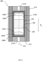
- FIG. 2 shows a configuration of a PVT growth structure 200 conventionally used in the vertical orientation for growing two single crystal boules 209A, 209B of a semiconductor material, such as SiC, simultaneously, and which can be advantageously employed by the present invention.
- the PVT growth structure 200 comprises a crucible 202 where a source material compartment 204 for the SiC source material 206 is provided in a central region that separates the crucible growth region in an upper and a lower growth compartment 210A and 210B. Seed crystals 208A and 208B are arranged in the separate growth compartments 210A and 210B, respectively, at a certain distance from the source material compartment 204 along a longitudinal axis 216.
- Each of the seed crystals 208A, 208B is cooled via a respective heat dissipation channel 212A, 212B to create a temperature gradient that transports the SiC vapor sublimed from the source material 206 towards the seeds 208A, 208B in the upper and lower growth compartments 210A and 210B.
- a respective heat dissipation channel 212A, 212B to create a temperature gradient that transports the SiC vapor sublimed from the source material 206 towards the seeds 208A, 208B in the upper and lower growth compartments 210A and 210B.
- Each of the upper and lower growth compartments 210A and 210B may be separated from the SiC source material 206 by a gas permeable porous barrier (not shown) to ensure that only gaseous Si and C containing components enter the growth compartments 210A and 210B.
- the crucible 202 is preferably made from a porous material, such as graphite, through which the upper and lower growth compartments 210A, 210B receive a doping gas or an inert gas.
- the crucible 202 may be surrounded by a porous, insulating material 214.
- This type of vertical growth structure is conventionally used in vertical PVT growth systems, such as the example illustrated in Fig. 3 .
- FIG. 3 shows a conventional PVT growth system 300 having a vertical reactor 301 with an inner chamber 304, where a PVT growth structure such 306 is vertically placed for growing the single crystal(s) under controlled temperature and vacuum conditions.
- the PVT growth system 300 includes an inductive heating system 310 arranged around the reactor 301 to heat the source material inside the PVT growth structure 306 to a suitable growth temperature.
- the inductive heating system 310 is generally provided as an induction coil 312, placed on the outside of the reactor 312 along the reactor longitudinal axis 318 and connected to a MF generator/inverter 314 that supplies a controlled current to the induction coil 312.
- the induction coil 312 induces the flow of electric current in the electrically conductive wall of the PVT growth structure 306, which generates sufficient heat to sublime the source material. For instance, temperatures of more than 2000° C, and particularly, of about 2200° C, are generally used for PVT growth of SiC single crystals.
- the height of the induction coil 312 may be adjustable to allow fine-tune of the source material temperature and temperature gradients established inside the PVT growth structure 306.
- the temperature reached inside the PVT growth structure 304 may be measured using one or more temperature sensors 316, such as pyrometers or thermocouples, located close to the heating channels of the PVT growth structure 306.
- the PVT growth system 300 also includes a pressure measuring system 320, possibly including a combination of pressure measuring devices, for measuring the pressure reached inside the reactor inner chamber 304.
- the PVT growth system 300 includes a vacuum pump system 330 with one or more vacuum/extraction pumps 332 (for e.g. a vacuum pump and/or a high vacuum pump) and an adjustable control valve 334 for controlling the suction power of the vacuum pump 332.
- a gas supply 340 supplies one or more gaseous compounds (such as Ar and N containing components) to the reactor inner chamber 304 to create a suitable doping or inert atmosphere for single crystal growth.
- the gas supply 340 may be an interface to compressed gas cylinders provided on site or to a central gas supply (not shown).
- the supply of doping and inert gases to the reactor 301 is individually controlled by a mass flow controller (MFC) 342.
- MFC mass flow controller
- a water cooling system 350 for dissipating the heat generated in the reactor 301 is provided, in general as two concentric and internally water-cooled glass tubes (not shown).
- the reactor 301 and inductive heating system 310 are in general enclosed in a shield or Faraday cage 370 to reduce electromagnetic radiation. Further components of the PVT growth system 300 includes metal flanges for sealing the reactor 301, including glass inserts for measuring the temperature by pyrometers (not shown).
- a system controller 380 which adjusts the growth process parameters and records all data of the single crystal growth process, such as pressure, temperature, position of the induction coil, cooling water temperature, and the like.
- Exemplary operation of a PVT growth system of the type illustrated in Fig. 3 is fully described in patent US 8,865,324 B2 , and therefore, it will not be further detailed here.
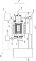
- Fig. 4 shows an inductive-heated PVT growth system 400 having a horizontally oriented reactor 401 for horizontal growth of semiconductor crystal boule(s) according to an embodiment.
- the inductive-heated PVT growth system 400 has substantially the same characteristics of the inductive-heated PVT growth system 300 described above, with the difference that it comprises a reactor 401 that is oriented with its longitudinal axis 418 along a direction transverse to gravity.
- the horizontal orientation of the reactor 401 makes possible to accommodate inside a single PVT growth structure, such as the PVT structure 200 described above, in an horizontal orientation, i.e. with its longitudinal axis 216 aligned with the longitudinal axis 416 of the reactor 401, such that the single crystals boules 209A, 209B now located on a left and right side of the horizontally oriented PVT growth structure 200 grow in a direction that is substantially horizontal.
- the growth direction and/or the longitudinal axis 216 of the PVT growth structure 200 do not have to necessarily make an horizontal angle of 0° (within a certain error margin) with the horizontal plane, i.e. the plane perpendicular to the direction of gravity F g , as illustrated in Fig. 4 .
- the reactor 401 and/or the PVT growth structure 200 inside the reactor 401 may be oriented such as to make a horizontal angle with the horizontal plane of less than a predetermined value, without departing from the principles of the present disclosure.
- the value of the horizontal angle of the reactor 401 and/or the PVT growth structure 200 lies between -15° and +15°.
- the lateral inner walls of the PVT growth structure 200 that surround the semiconductor crystal boules 209A, 209B become essentially transverse to the gravity direction, and consequently, the graphite/carbon particles released therefrom, or at least most part, will fall by gravity on the lower inner wall of the PVT growth structure 200.
- the PVT growth system 400 includes dedicated inductive heating system 410 with heating coils 412 that are supplied with a current from a MF generator 414 under the control of a system controller 480.
- the temperature reached in the reactor inner chamber may be measured and monitored using suitable temperature sensors 416, which are controlled by the system controller 480.
- the reactor 401 is also provided with cooling system 450, which is individually controlled and/or monitored by the system controller 480.
- FIG. 5 shows an inductive-heated PVT growth system 500 having a horizontally oriented reactor 501 for horizontal growth of semiconductor crystal boule(s) according to a further embodiment, which essentially differs from the PVT system 400 illustrated in Fig. 4 in that it comprises a reactor 501 with a single glass tube.
- the dissipation of heat from the reactor 501 is not achieved by water cooling but rather by a flux of air, which is passed around the outer edge of the glass tube in a controlled manner.
- the reactor 501 is oriented horizontally such as to accommodate a PVT growth structure, such as the PVT growth structure 200 described above, in a substantial horizontal orientation, i.e.
- the PVT growth system 500 also comprises process control systems, including a inductive heating system 510, pressure measuring system 520, vacuum pump system 530, gas supply system 540, inductive heating and air cooling systems, which are similar to those described with reference to the PVT growth system 300 described above and controlled by a system controller 580 in a similar manner, and therefore, these will not be further detailed here.
- process control systems including a inductive heating system 510, pressure measuring system 520, vacuum pump system 530, gas supply system 540, inductive heating and air cooling systems, which are similar to those described with reference to the PVT growth system 300 described above and controlled by a system controller 580 in a similar manner, and therefore, these will not be further detailed here.
- Fig. 6 shows an resistive-heated PVT growth system 600 having a horizontally oriented reactor 601 for horizontal growth of semiconductor crystal boule(s) according to a further embodiment, and which essentially differs from the PVT systems 400 and 500 described above in that it uses using a heating system 660 of a resistive type instead.
- the reactor 601 has an inner chamber 604 that accommodates an horizontally oriented PVT growth structure 602, similar to the PVT growth structure 200 described above but without insulating material covering the lateral walls due to the resistive heating.
- the resistive heating system 660 includes resistive heating elements 662 mounted inside the reactor 601.
- a heating current control unit 664 supplies current to the resistive heating elements 662 to heat the reactor inner chamber 604 in a controlled manner and achieve a suitable growth temperature.
- the reactor 601 may be made with walls of metal and provided with a respective water cooling system 650. Alternatively, an air cooling system, such as the one described above with reference to Fig. 5 , may be used.
- the PVT growth system 600 also comprises process control systems, such as a pressure measuring system 620, vacuum pump system 630, and gas supply system 640, which are similar to those described with reference to the PVT growth system 300 described above and controlled by a system controller 680 in a similar manner, and therefore, these will not be further detailed here.
- a PVT growth system may be provided having a plurality of horizontally oriented reactors, such as any of the reactors of the PVT growth systems 400, 500, 600, described above, and which are connected via a common channel vacuum to a common vacuum system.
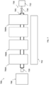
- Figure 7 shows a PVT growth system 700 comprising N reactors 700A to 700N for growing more than one semiconductor single crystal simultaneously and which are connected to each other via a common vacuum channel 705.
- the reactors 700A to 700N are horizontally oriented, i.e. their longitudinal axis lie substantially on the horizontal plane transverse to the gravity direction, and are preferably of a same type, such as to be operated at a same gas phase pressure conditions during the single crystals growth.
- the common vacuum channel 705 connects the N reactors 700A to 700N to a common vacuum pump system 730 in a serial manner so that one of the reactors is directly connected to the vacuum pump 732 whereas the other reactor(s) are evacuated via the common vacuum channel 705.
- the vacuum conditions and/or pressure in the reactors inner chambers are centrally controlled by the system controller 780 via an adjustable control valve 734 provided between the vacuum pump 632 and the reactor 700N at the end of the vacuum channel 605 that is closer to the vacuum pump 732.
- the pressure inside the inner chambers of reactors 700A to 700N can be controlled simultaneously in a centralized manner and without the need of separate vacuum systems and controllers for each reactor.
- the PVT growth system 700 also includes a pressure measurement system 720 having one or more pressure sensors that may be arranged in at least one of the reactors 700A to 700N to perform measurements indicative of a pressure reached in the respective reactor inner chambers.
- a suitable doping and/or inert gaseous atmosphere for the single crystals growth is achieved in the inner chambers of each reactor 700A to 700N by supplying the gaseous components that form the doping/inert gaseous atmosphere via individual gas feeds from a gas supply (not shown), and which are individually controlled by the system controller 780 via dedicated mass flux controllers.
- the pressure measurement system 720 monitors the pressure measured by the pressure sensor(s), and outputs vacuum control parameters for controlling the adjustable control valve 734 to regulate the pressure inside the reactors inner chambers to a predetermined pressure.
- the pressure measurement system 720 outputs also gas phase control parameters, based on the monitored pressure, for the MFCs controlling the supply of the gaseous components into the reactors inner chambers, such as to achieve and maintain substantially the same predetermined gas phase conditions (i.e. pressure an composition of the doping/inert gas atmosphere) over all the reactors connected via the common vacuum channel 705.
- each reactor 700A to 700N may be of any type, such as the reactors 401, 501, 601 of the PVT growth systems 400, 500 and 600 described above, for which respective heating systems are provided and controlled via respective MF generators to reach the required temperature conditions in each reactors 700A to 700N individually and using individual growth process parameters for each reactor 700A to 700N.
- the temperature reached in the reactors inner chambers may be measured and monitored using suitable temperature sensors under control of the system controller 780.
- the reactors 700A to 700N are provided with respective cooling systems, which are individually controlled and/or monitored by the system controller 780, for dissipating heat from the respective reactors 700A to 700N.
- the cooling systems may be based on water cooling or air cooling system, depending on the type of reactor such as described above.
- the operation of the inductive heating system, cooling system, and temperature control is essentially the same as in the conventional PVT growth system 300 described above with reference to Fig. 3 , and may be controlled individually or using a common controller or PC, in order to save space and equipment costs.
- the pressure sensor(s) measure the pressure at the reactor 700A that is more distant from the reactor 700N directly connected to the vacuum pump system 730 along the common vacuum path 705.
- the pressure sensor(s) may be located to measure pressure on the top side of the reactor 700A.
- the pressure sensor(s) may also be provided in a bottom side of the reactor 700A.
- the amount of doping or inert gases can be supplied to all reactors simultaneously by a common gas duct under control of a common MFC, thereby, eliminating supply differences due to slight differences in response from individual MFCs and facilitating the growth process control.
- measurement and monitoring of pressure inside the reactors inner chambers may be performed by pressure sensors located on only one of the reactors without significant loss of accuracy, with additional savings on space and equipment costs.
- the number N of reactors connected by a common vacuum channel 705 in the PVT growth system 700 shown in Fig. 7 can be selected as any integer between 2 and 20, and more preferably, between 6 and 10. Such a limitation on the number of connected reactors may be desirable to avoid imposing high demands on the exhaustion capabilities of the vacuum pump system 730 while allowing to reach a suitable vacuum condition for the growth process within an acceptable time for most applications. Thus, any of the vacuum pump systems used in conventional PVT growth systems using a single reactor may be advantageously employed as the vacuum pump system 730 in the PVT growth system 700.
- the number N of reactors connected to the common vacuum channel 705 does not need to be fixed and may easily be increased or decreased according to need by simply adding or removing the vacuum connections of the additional or unnecessary reactors to the common vacuum channel.
- the present invention makes possible to manufacture one or a plurality of single crystal simultaneously while reducing or even eliminating contamination effects due to graphite/carbon particles by using horizontally oriented PVT growth systems and/or horizontally oriented PVT growth reactors.
- the horizontal orientation also makes possible to, for instance, make use of PVT growth structures designed to allow simultaneous growth of two crystals, such as described above with reference to Fig. 2 , without the disadvantage of the lower crystal being contaminated by graphite/carbon particles.
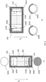
- Fig. 8 illustrates the effects of graphite/carbon contamination with reference to the crucible 202 of the PVT growth structure 200 during simultaneous growth of two semiconductor crystal boules 209A, 209B on the upper and lower growth compartments 210A, 210B when the PVT growth structure is oriented in: (a) a vertical orientation; and (b) horizontal orientation with respect to the gravity direction (F g ).
- the semiconductor boule 209B growing in the lower growth compartment 210B is strongly contaminated with released graphite/carbon particles falling in the direction of the lower crystal seed 208B by the effect of gravity, in comparison with the semiconductor boule 209B growing in the upper compartment 210A, which remains essentially unaffected by graphite/carbon contamination during the whole growth process.
- the contaminating graphite/carbon particles come from, for example the cylindrical wall of the lower compartment 210B that is concentrically arranged around the crystal 209B and along the crucible longitudinal axis 216, from the material of a membrane (not shown) that separates the source material from the lower growth compartment 210B, and/or other parts of the PVT growth structure that surround the crystal or which are used closed thereto.
- the growth process may follow one or both of the process conditions described below.
- h MIN e.g. h ⁇ 2 mm
- the graphite/carbon particles falling from the crucible inner walls and/or the membrane may hint onto the growing crystal 209B (or 209A) and form inclusions, which would lead to a considerable "upper half" 222B of the horizontally growing crystal being interspersed with graphite/carbon particles, as shown in Fig. 9 (c) .
- the graphite/carbon particles may still touch the growth surface 220B of the crystal boule 209B but fall due to the gravitational force on the lower, inner side wall of the growth crucible 202 without being incorporated in the crystal 209A itself. At most, only a thin upper layer 222B on the semiconductor boule 209B might be affected.
- suitable growth process parameters for achieving a corresponding curvature of the growth surfaces 220A, 220B may be determined based on characteristics of the reactor and respective crucible, the required diameter and length for the semiconductor boules 209A, 209B, the substrate diameter s, and the required temperatures for the PVT growth process, for instance based on simulation analysis.
- a second process condition is that the base of the crystal seed 208A used for the monocrystal growth has a diameter of at least 10% larger than the diameter of the inclusion-free cross-section s.
- This second condition addresses the shortcoming that the requirement of the first condition described above for the curvature of the growth surface 220A cannot be met in the edge region of the crystal boule 209A.
- the local curvature of the growth surface 220A in the edge region is preferably significantly larger to avoid that the crystal boule 209A grows together with the inner wall of the crucible 202.
- Graphite/carbon particles will then always build-up in the edge region of the single crystal boule, which may be later removed by subsequent processing of the crystal boule to the final substrate diameter (for e.g., by cylindrical grinding).
- a seed with a diameter that is substantially equal to an outer diameter of the single crystal to be grown therein and at least 10% larger than a predetermined diameter for a substrate to be made from the single crystal, and most preferably, a seed crystal diameter that is 10% to 35% larger than the predetermined substrate diameter.
- the present invention provides a novel concept of PVT growth systems for manufacturing one semiconductor single crystal boule or more than one semiconductor single crystal boules simultaneously in a horizontal growth direction, which allows to increase the rate of production of semiconductor single crystals while ensuring homogeneous high quality crystals, and thereby reduces losses due to rejection, in comparison with semiconductor single crystals manufactured in PVT growth systems based on the vertically oriented reactor and/or vertical crucible concept.
- a further advantage of the PVT growth systems according to the present invention can be seen in the fact that it may be advantageously implemented using any type of vertical growth reactor. Further, by connecting several horizontal reactors via a common vacuum channel to a common vacuum pump system, it is possible to simultaneously manufacture more than one semiconductor single crystal boules by making use of conventional crucibles in horizontally orientation, i.e. without the need of changing the crucible dimensions and/or the amount of source materials, which results in cost savings in comparison with PVT growth systems that use crucibles with an enlarged diameter for enclosing several crystal seeds and an enlarged material source.
Landscapes
- Chemical & Material Sciences (AREA)
- Engineering & Computer Science (AREA)
- Crystallography & Structural Chemistry (AREA)
- Materials Engineering (AREA)
- Metallurgy (AREA)
- Organic Chemistry (AREA)
- Inorganic Chemistry (AREA)
- Chemical Kinetics & Catalysis (AREA)
- General Chemical & Material Sciences (AREA)
- Crystals, And After-Treatments Of Crystals (AREA)
Claims (16)
- Procédé de fabrication d'un ou plusieurs monocristaux de semi-conducteur (209A, 209B) par transport physique en phase vapeur (PVT) ayant une section transversale exempte d'inclusions, transversale à la direction de croissance, qui est exempte d'inclusions au sein d'un diamètre prédéterminé, comprenant :la croissance desdits un ou plusieurs monocristaux de semi-conducteur (209A, 209B) dans une structure de croissance par PVT (200) en utilisant un processus de croissance par PVT, la structure de croissance par PVT (200) comprenant un creuset (102 ; 202), un compartiment de matériau source (204) à l'intérieur du creuset (202) et un ou plusieurs germes cristallins (208A, 208B) disposés à l'intérieur du creuset (102 ; 202) à une distance, le long d'un axe longitudinal (116 ; 216) de la structure de croissance par PVT (200), du compartiment de matériau source (104 ; 204), pour faire croître, respectivement, lesdits un ou plusieurs monocristaux de semi-conducteur (209A, 209B) dans la direction dudit axe longitudinal (216),la structure de croissance par PVT (200) étant logée dans une chambre interne (404 ; 504 ; 604) d'un réacteur (401 ; 501 ; 601) suivant une orientation sous laquelle l'axe longitudinal (216) de la structure de croissance par PVT (200) est sensiblement horizontal ou forme un angle avec l'horizontale qui est dans une plage entre -15° et +15° par rapport à un plan horizontal perpendiculaire à la direction de la pesanteur, de sorte qu'une direction de croissance desdits un ou plusieurs monocristaux de semi-conducteur (209A, 209B) à l'intérieur de la structure de croissance par PVT (200) soit respectivement sensiblement horizontale ou à l'intérieur de ladite plage d'angle avec l'horizontale, etla croissance desdits un ou plusieurs monocristaux de semi-conducteur dans la structure de croissance par PVT (200) comprenant la commande des températures de croissance et d'au moins l'une parmi la pression à l'intérieur de la chambre interne et l'alimentation gazeuse en gaz dopants et/ou inertes dans la chambre interne ;
caractérisé parla fourniture d'un ou plusieurs germes cristallins (208A, 208B) ayant un diamètre qui est sensiblement égal à un diamètre extérieur du monocristal de semi-conducteur (209A, 209B) à faire croître ici et supérieur d'au moins 10 % au diamètre prédéterminé de ladite section transversale exempte d'inclusions ; etla réalisation du processus de croissance par PVT en utilisant des paramètres de processus de croissance par PVT prédéterminés qui sont déterminés par une analyse de simulation basée sur des caractéristiques du réacteur et la structure de croissance par PVT (200), le diamètre et la longueur du ou des plusieurs monocristaux de semi-conducteur (209A, 209B) à faire croître à l'intérieur de la structure de croissance par PVT (200), le diamètre prédéterminé de la ou des sections transversales exemptes d'inclusions, et les températures du processus de croissance par PVT, de façon à obtenir une surface de croissance (220A, 220B) correspondante présentant une courbure convexe de hauteur maximale (h) qui est maintenue dans une plage de hauteur prédéterminée entre 2 mm et 8 mm pendant le processus de croissance par PVT et au niveau de laquelle ladite section transversale exempte d'inclusions ayant le diamètre prédéterminé est formée sur chaque monocristal de semi-conducteur (209A, 209B),ladite hauteur maximale (h) correspondant à une distance maximale, dans la direction de croissance, entre la surface de croissance (220A, 220B) convexe et une section transversale du monocristal de semi-conducteur (209A, 209B) respectif, qui est sécante de la surface de croissance (220A, 220B) convexe, dans un plan transversal à la direction de croissance, au niveau d'une région où le diamètre extérieur du monocristal de semi-conducteur (209A, 209B) est sensiblement égal audit diamètre prédéterminé de la section transversale exempte d'inclusions, etladite plage de hauteur prédéterminée étant indépendante du diamètre prédéterminé de la ou des sections transversales exemptes d'inclusions et du diamètre du germe cristallin (208A, 208B) respectif. - Procédé selon la revendication 1, dans lequel
le réacteur est orienté horizontalement par rapport au sens de la pesanteur pour loger ladite structure de croissance par PVT. - Procédé selon la revendication 1 ou 2, dans lequel
la plage de hauteur prédéterminée va, de préférence, de 4 mm à 6 mm. - Procédé selon l'une quelconque des revendications 1 à 3, dans lequelle diamètre du germe cristallin est 10 % à 35 % supérieur audit diamètre de substrat prédéterminé ; et/oudans lequel lesdits un ou plusieurs monocristaux de semi-conducteur (209A, 209A) sont des monocristaux d'un matériau semi-conducteur d'un groupe comprenant au moins du carbure de silicium, 4H-SiC et un semi-conducteur contenant des éléments des groupes III à V.
- Procédé selon l'une quelconque des revendications 1 à 4, comprenant en outre :la croissance d'une pluralité de monocristaux de semi-conducteur dans deux réacteurs (700A à 700N) ou plus qui sont reliés entre eux et à un système de pompe à vide via un canal de vide commun (705), chaque réacteur ayant une chambre interne conçue pour loger une structure de croissance par PVT (200) pour faire croître un ou plusieurs monocristaux de semi-conducteur à l'intérieur, le réacteur étant conçu pour loger ladite structure de croissance par PVT (200) selon une orientation par rapport à la direction de la pesanteur telle qu'une direction de croissance desdits un ou plusieurs monocristaux de semi-conducteur à l'intérieur de la structure de croissance par PVT (200) est sensiblement horizontale ou dans un angle avec l'horizontale inférieur à ladite valeur prédéterminée ; etla création et/ou la commande, avec ledit système de pompe à vide, d'un état de phase gazeuse commun dans les chambres internes desdits deux réacteurs (700A à 700N) reliés ou plus.
- Procédé selon la revendication 5, comprenant en outre :la réalisation de mesures indicatives d'une pression de l'état de phase gazeuse atteint dans les chambres internes des deux réacteurs reliés ou plus au moyen d'un ou plusieurs capteurs de pression disposés dans l'un au moins des deux réacteurs reliés ou plus ; etla surveillance desdites mesures de pression, l'émission en sortie de paramètres de commande de vide pour commander ledit système de pompe à vide et l'émission en sortie de paramètres de commande de phase gazeuse pour commander un système d'alimentation en gaz pour alimenter des composants gazeux qui forment ladite phase gazeuse dans les chambres internes de façon à atteindre et maintenir sensiblement un état de phase gazeuse identique prédéterminé dans toutes les chambre internes reliées,ledit état de phase gazeuse incluant la pression et/ou la composition de ladite phase gazeuse.
- Procédé selon la revendication 6, dans lequellesdites mesures indicatives de la pression dudit état de phase gazeuse étant réalisées au niveau d'un réacteur, parmi les deux réacteurs reliés ou plus, qui est le plus distant d'un raccordement au système de pompe à vide le long du canal de vide commun ; et/oulesdites mesures de pression indicatives de la pression dudit état de phase gazeuse étant réalisées sur le canal de vide commun sur une région inférieure des deux réacteurs reliés ou plus.
- Procédé selon l'une quelconque des revendications 1 à 7, comprenant en outre :la commande des paramètres du processus de croissance par PVT dans les deux réacteurs (700A à 700N) ou plus au moyen d'un module de commande de système commun,lesdits paramètres de processus de croissance par PVT comprenant en outre l'une au moins parmi la pression à l'intérieur des chambres internes desdits réacteurs, la température de croissance et l'alimentation gazeuse en gaz dopants et/ou inertes dans les chambre internes, et/oula commande, au moyen du module de commande de système commun, d'un système de chauffage et d'un système de refroidissement de chaque réacteur, le système de chauffage étant l'un parmi un système de chauffage inductif et un système de chauffage résistif, et le système de refroidissement étant l'un ou une combinaison d'un système de refroidissement à eau et d'un système de refroidissement à air.
- Procédé de croissance par transport physique en phase vapeur (PVT) pour la fabrication d'un ou plusieurs monocristaux de semi-conducteur (209A, 209B) tel que le ou les monocristaux de semi-conducteur (209A, 209B) ont une section transversale exempte d'inclusions, transversale à la direction de croissance, qui est exempte d'inclusions au sein d'un diamètre prédéterminé, le système comprenant :une structure de croissance par PVT (200) comprenant :un creuset (102 ; 202),un compartiment de matériau source (204) à l'intérieur du creuset (202), etun ou plusieurs germes cristallins (208A, 208B) disposés à l'intérieur du creuset (102 ; 202) à une distance, le long d'un axe longitudinal (116 ; 216) de la structure de croissance par PVT (200), du compartiment de matériau source (104 ; 204), pour faire respectivement croître lesdits un ou plusieurs monocristaux de semi-conducteur (209A, 209B) dans la direction dudit axe longitudinal (216) ; etun module de commande de système conçu pour commander des paramètres d'un processus de croissance par PVT pour faire croître lesdits un ou plusieurs monocristaux de semi-conducteur (209A, 209B) à l'intérieur de la structure de croissance par PVT (200), les paramètres du processus de croissance par PVT incluant des températures de croissance et l'une au moins parmi la pression à l'intérieur de la chambre interne et l'alimentation gazeuse en gaz dopants et/ou inertes dans la chambre interne ;etun réacteur (401 ; 501 ; 601) orienté suivant un axe longitudinal qui est sensiblement horizontal ou qui forme un angle avec l'horizontale qui est dans une plage entre -15° et +15° par rapport à un plan horizontal plan perpendiculaire à la direction de la pesanteur, le réacteur ayant :une chambre interne (404 ; 504 ; 604) conçue pour loger ladite structure de croissance par PVT (200) à l'intérieur suivant une orientation dans laquelle l'axe longitudinal de la structure de croissance par PVT (200) est aligné avec l'axe longitudinal (416 ; 516 ; 616) du réacteur (401 ; 501 ; 601) de sorte qu'une direction de croissance desdits un ou plusieurs monocristaux de semi-conducteur (209A, 209B) à l'intérieur de la structure de croissance par PVT (200) est sensiblement horizontale ou dans ladite plage d'angle horizontal, respectivement ; etun système de chauffage (410, 510, 660) conçu pour chauffer la structure de croissance par PVT (200) logée à l'intérieur de la chambre interne (404 ; 504 ; 604) suivant ladite orientation ;caractérisé en ce que chacun des germes cristallins (208A, 208B) a un diamètre qui est sensiblement égal à un diamètre extérieur du monocristal de semi-conducteur (209A, 209B) à faire croître ici et supérieur d'au moins 10 % au diamètre prédéterminé de ladite section transversale exempte d'inclusions, etdans lequel le module de commande du système, pendant le fonctionnement, surveille et commande le système de chauffage (410, 510, 660) pendant le processus de croissance par PVT avec des paramètres de processus de croissance par PVT prédéterminés, qui sont déterminés pour ledit réacteur par une analyse de simulation basée sur des caractéristiques du réacteur et de la structure de croissance par PVT (200), le diamètre et la longueur du ou des plusieurs monocristaux de semi-conducteur (209A, 209B) à faire croître à l'intérieur de la structure de croissance par PVT (200), le diamètre prédéterminé de la section transversale exempte d'inclusion, et des températures du processus de croissance par PVT, et auxquels une surface de croissance correspondante (220A, 220B) présentant une courbure convexe de hauteur maximale (h) est maintenue dans une plage de hauteur prédéterminée entre 2 mm et 8 mm pendant le processus de croissance par PVT pour former ladite section transversale exempte d'inclusions ayant le diamètre prédéterminé sur chaque monocristal de semi-conducteur (209A, 209B),ladite hauteur maximale (h) correspondant à une distance maximale, dans la direction de croissance, entre la surface de croissance (220A, 220B) convexe et une section transversale du monocristal de semi-conducteur (209A, 209B) respectif, qui est sécante de la surface de croissance (220A, 220B) convexe, dans un plan transversal à la direction de croissance, au niveau d'une région où le diamètre extérieur du monocristal de semi-conducteur (209A, 209B) est sensiblement égal audit diamètre prédéterminé de la section transversale exempte d'inclusions, etladite plage de hauteur prédéterminée étant indépendante du diamètre prédéterminé de la ou des sections transversales exemptes d'inclusions et du diamètre du germe cristallin (208A, 208B) respectif.
- Système selon la revendication 9, dans lequel
ladite plage de hauteur prédéterminée va, de préférence, de 4 mm à 6 mm. - Système selon la revendication 9 ou 10, dans lequella structure de croissance par PVT (200) comprend un compartiment de matériau source (204) central contenant un matériau source (206) et deux compartiments de croissance (210A, 210B), un sur chaque côté du compartiment de matériau source (204) central, un germe cristallin étant placé sur chaque compartiment de croissance et à une certaine distance le long de l'axe longitudinal (216) à partir du matériau source central pour faire croître des monocristaux respectifs à partir du même matériau source ;ledit matériau source étant choisi pour faire croître des monocristaux d'un matériau semi-conducteur d'un groupe comprenant au moins du carbure de silicium, 4H-SiC et un semi-conducteur contenant des éléments des groupes III à V.
- Système selon l'une quelconque des revendications 9 à 11, comprenant en outre :une pluralité de réacteurs (700A à 700N), chaque réacteur ayant une chambre interne conçue pour loger une structure de croissance par PVT (200) respective pour faire croître un ou plusieurs monocristaux de semi-conducteur à l'intérieur, chaque réacteur et structure de croissance par PVT (200) respective étant orientés horizontalement par rapport à la direction de la pesanteur de sorte que la direction de croissance desdits un ou plusieurs monocristaux dans la structure de croissance par PVT (200) soit sensiblement horizontale ou dans ledit angle avec l'horizontale ;un canal de vide commun (705) raccordable à un système de pompe à vide ;deux réacteurs ou plus de ladite pluralité de réacteurs (700A à 700N) étant conçus pour être raccordés en série au système de pompe à vide, via ledit canal de vide commun (705), afin de créer et/ou commander un état de phase gazeuse commun dans les chambres internes desdits deux réacteurs reliés ou plus.
- Système selon la revendication 12, comprenant en outre :un système de mesure de pression comprenant un ou plusieurs capteurs de pression disposés dans au moins l'un des deux réacteurs ou plus reliés via le canal de vide commun (705) pour réaliser des mesures indicatives d'une pression de l'état de phase gazeuse atteint dans les chambres internes respectives ;ledit système de mesure de pression étant conçu pour surveiller lesdites mesures de pression, et pour émettre en sortie des paramètres de commande de vide pour commander ledit système de pompe à vide et des paramètres de commande de phase gazeuse pour commander un système d'alimentation en gaz pour fournir des composants gazeux qui forment ladite phase gazeuse dans les chambres internes de façon à atteindre et maintenir un état de phase gazeuse sensiblement identique et prédéterminé dans toutes les chambres internes reliées, etledit état de phase gazeuse incluant la pression et/ou la composition de ladite phase gazeuse.
- Système selon la revendication 13, dans lequelle ou les plusieurs capteurs de pression sont conçus pour réaliser des mesures indicatives de la pression de l'état de phase gazeuse au niveau d'un réacteur parmi lesdits deux réacteurs reliés ou plus qui est le plus distant d'un raccordement au système de pompe à vide le long du canal de vide commun (705) ; et/oule ou les plusieurs capteurs de pression sont conçus pour réaliser des mesures indicatives de la pression dudit état de phase gazeuse sur le canal de vide commun (705) au niveau d'une région inférieure des deux réacteurs reliés ou plus.
- Système selon l'une quelconque des revendications 9 à 14, comprenant en outre :un système de refroidissement conçu pour dissiper de la chaleur du réacteur, le système de refroidissement étant l'un ou une combinaison d'un système de refroidissement à eau et d'un système de refroidissement à air ;le système de chauffage étant l'un parmi un système de chauffage inductif et un système de chauffage résistif.
- Système selon l'une quelconque des revendications 9 à 15, dans lequelle module de commande du système est en outre conçu pour commander les paramètres du processus de croissance par PVT dans la pluralité de réacteurs (700A à 700N),lesdits paramètres du processus de croissance par PVT incluant l'une au moins parmi la pression à l'intérieur de la chambre interne de chaque réacteur, la température de croissance et l'alimentation gazeuse en gaz dopants et/ou inertes dans la chambre interne de chaque réacteur.
Priority Applications (4)
| Application Number | Priority Date | Filing Date | Title |
|---|---|---|---|
| EP19184259.0A EP3760765B1 (fr) | 2019-07-03 | 2019-07-03 | Système de croissance horizontale de monocristaux à semiconducteur de haute qualité et son procédé de fabrication |
| JP2020038469A JP7184836B2 (ja) | 2019-07-03 | 2020-03-06 | 高品質半導体単結晶の水平成長のためのシステム、およびそれを製造する方法 |
| CN202010419654.3A CN112176405B (zh) | 2019-07-03 | 2020-05-18 | 水平生长高质量半导体单晶的系统及该单晶的制造方法 |
| US16/894,337 US11479875B2 (en) | 2019-07-03 | 2020-06-05 | System for horizontal growth of high-quality semiconductor single crystals by physical vapor transport |
Applications Claiming Priority (1)
| Application Number | Priority Date | Filing Date | Title |
|---|---|---|---|
| EP19184259.0A EP3760765B1 (fr) | 2019-07-03 | 2019-07-03 | Système de croissance horizontale de monocristaux à semiconducteur de haute qualité et son procédé de fabrication |
Publications (2)
| Publication Number | Publication Date |
|---|---|
| EP3760765A1 EP3760765A1 (fr) | 2021-01-06 |
| EP3760765B1 true EP3760765B1 (fr) | 2022-03-16 |
Family
ID=67180566
Family Applications (1)
| Application Number | Title | Priority Date | Filing Date |
|---|---|---|---|
| EP19184259.0A Active EP3760765B1 (fr) | 2019-07-03 | 2019-07-03 | Système de croissance horizontale de monocristaux à semiconducteur de haute qualité et son procédé de fabrication |
Country Status (4)
| Country | Link |
|---|---|
| US (1) | US11479875B2 (fr) |
| EP (1) | EP3760765B1 (fr) |
| JP (1) | JP7184836B2 (fr) |
| CN (1) | CN112176405B (fr) |
Families Citing this family (6)
| Publication number | Priority date | Publication date | Assignee | Title |
|---|---|---|---|---|
| EP3760766B1 (fr) * | 2019-07-03 | 2022-03-09 | SiCrystal GmbH | Système de fabrication efficace d'une pluralité de monocristaux semiconducteur à haute qualité et son procédé de fabrication |
| CN113293438A (zh) * | 2021-06-01 | 2021-08-24 | 中科汇通(内蒙古)投资控股有限公司 | 一种具有双生长腔室的翻转式SiC单晶生长装置 |
| DE102021123991B4 (de) | 2021-09-16 | 2024-05-29 | Pva Tepla Ag | PVT-Verfahren und Apparatur zum prozesssicheren Herstellen von Einkristallen |
| JP2025531119A (ja) | 2022-09-16 | 2025-09-19 | ピー・ヴィ・エー テプラ アー・ゲー | 単結晶のプロセス安全生産のためのpvt方法および装置 |
| DE102022123757B4 (de) | 2022-09-16 | 2024-05-29 | Pva Tepla Ag | Apparatur, Tragrahmen für eine Apparatur und PVT-Verfahren zum prozesssicheren Herstellen von Einkristallen |
| DE102022123747A1 (de) | 2022-09-16 | 2024-03-21 | Pva Tepla Ag | PVT-Verfahren und Apparatur zum prozesssicheren Herstellen von Einkristallen |
Family Cites Families (23)
| Publication number | Priority date | Publication date | Assignee | Title |
|---|---|---|---|---|
| DE4310744A1 (de) * | 1993-04-01 | 1994-10-06 | Siemens Ag | Vorrichtung zum Herstellen von SiC-Einkristallen |
| US20050178336A1 (en) | 2003-07-15 | 2005-08-18 | Heng Liu | Chemical vapor deposition reactor having multiple inlets |
| US20050011459A1 (en) * | 2003-07-15 | 2005-01-20 | Heng Liu | Chemical vapor deposition reactor |
| JP4586958B2 (ja) | 2004-01-14 | 2010-11-24 | 信越半導体株式会社 | 単結晶引上げ設備及び真空排気方法 |
| GB2423307A (en) | 2005-02-22 | 2006-08-23 | Univ Durham | Apparatus and process for crystal growth |
| US7279040B1 (en) * | 2005-06-16 | 2007-10-09 | Fairfield Crystal Technology, Llc | Method and apparatus for zinc oxide single crystal boule growth |
| US7942970B2 (en) * | 2005-12-20 | 2011-05-17 | Momentive Performance Materials Inc. | Apparatus for making crystalline composition |
| US7524376B2 (en) | 2006-05-04 | 2009-04-28 | Fairfield Crystal Technology, Llc | Method and apparatus for aluminum nitride monocrystal boule growth |
| JP2009155137A (ja) | 2007-12-25 | 2009-07-16 | Fujikura Ltd | 化合物半導体結晶の製造方法及び単結晶製造装置 |
| JP2010037189A (ja) | 2008-07-08 | 2010-02-18 | Sumitomo Electric Ind Ltd | 結晶成長装置および結晶成長方法 |
| DE112009003667B4 (de) | 2008-12-08 | 2024-04-25 | Ii-Vi Inc. | Verbessertes axial-gradient-transport- (agt-) züchtungsverfahren und -apparat unter anwendung von resistivem erhitzen |
| CN201545935U (zh) * | 2009-09-02 | 2010-08-11 | 吴晟 | 一种用于控制真空生长室内气体压力的压力自动控制装置 |
| DE102010029756B4 (de) | 2010-06-07 | 2023-09-21 | Sicrystal Gmbh | Herstellungsverfahren für einen SiC-Volumeneinkristall mit großer Facette und einkristallines SiC-Substrat mit homogener Widerstandsverteilung |
| US20120058630A1 (en) | 2010-09-08 | 2012-03-08 | Veeco Instruments Inc. | Linear Cluster Deposition System |
| CN102732953B (zh) * | 2011-04-12 | 2017-04-19 | 李汶军 | 双籽晶辅助气相传输方法生长碳化硅单晶的技术和装置 |
| CN104246023B (zh) * | 2012-04-20 | 2019-02-01 | 贰陆股份公司 | 大直径高品质的SiC单晶、方法和设备 |
| EP2664695B1 (fr) * | 2012-05-16 | 2015-07-15 | SiCrystal AG | Système de croissance de transport de vapeur physique pour la croissance simultanée de plus d'un mono-cristal de SiC et procédé de croissance |
| CN110670124B (zh) | 2013-09-06 | 2021-07-30 | Gtat公司 | 生产大块硅碳化物的方法 |
| US20160138185A1 (en) | 2014-11-18 | 2016-05-19 | Sumitomo Electric Industries, Ltd. | Method of manufacturing silicon carbide single crystal |
| JPWO2017057742A1 (ja) | 2015-10-02 | 2018-07-19 | 昭和電工株式会社 | SiC単結晶インゴット |
| US20170321345A1 (en) | 2016-05-06 | 2017-11-09 | Ii-Vi Incorporated | Large Diameter Silicon Carbide Single Crystals and Apparatus and Method of Manufacture Thereof |
| KR101806423B1 (ko) * | 2017-03-16 | 2017-12-07 | 주식회사 사파이어테크놀로지 | 탄화규소 단결정 잉곳의 멀티 성장장치 |
| EP3760766B1 (fr) * | 2019-07-03 | 2022-03-09 | SiCrystal GmbH | Système de fabrication efficace d'une pluralité de monocristaux semiconducteur à haute qualité et son procédé de fabrication |
-
2019
- 2019-07-03 EP EP19184259.0A patent/EP3760765B1/fr active Active
-
2020
- 2020-03-06 JP JP2020038469A patent/JP7184836B2/ja active Active
- 2020-05-18 CN CN202010419654.3A patent/CN112176405B/zh active Active
- 2020-06-05 US US16/894,337 patent/US11479875B2/en active Active
Also Published As
| Publication number | Publication date |
|---|---|
| JP7184836B2 (ja) | 2022-12-06 |
| US20210002787A1 (en) | 2021-01-07 |
| JP2021011423A (ja) | 2021-02-04 |
| EP3760765A1 (fr) | 2021-01-06 |
| US11479875B2 (en) | 2022-10-25 |
| CN112176405B (zh) | 2022-11-29 |
| CN112176405A (zh) | 2021-01-05 |
Similar Documents
| Publication | Publication Date | Title |
|---|---|---|
| EP3760765B1 (fr) | Système de croissance horizontale de monocristaux à semiconducteur de haute qualité et son procédé de fabrication | |
| EP3760766B1 (fr) | Système de fabrication efficace d'une pluralité de monocristaux semiconducteur à haute qualité et son procédé de fabrication | |
| US12460314B2 (en) | Silicon carbide substrate and method of growing SiC single crystal boules | |
| EP2664695B1 (fr) | Système de croissance de transport de vapeur physique pour la croissance simultanée de plus d'un mono-cristal de SiC et procédé de croissance | |
| KR101760030B1 (ko) | 대구경 탄화규소 단결정 성장 장치로부터 소구경 탄화규소 단결정을 성장시키는 방법 및 장치 | |
| EP3276050B1 (fr) | Procédé de production de monocristal de carbure de silicium | |
| EP1205583B1 (fr) | Procédé et appareillage pour la production des cristaux de carbure de silicium à partir des sources gazeuse | |
| US10801126B2 (en) | Method for producing bulk silicon carbide | |
| KR102276450B1 (ko) | 탄화규소 잉곳의 제조방법, 탄화규소 웨이퍼의 제조방법 및 이의 성장 시스템 | |
| US20240044044A1 (en) | Crystal growth device and method for growing a semiconductor | |
| JP7242978B2 (ja) | SiC単結晶インゴットの製造方法 | |
| JP2619611B2 (ja) | 単結晶の製造装置および製造方法 | |
| JP2025097954A (ja) | SiCボリューム単結晶を生成するための坩堝、およびSiCボリューム単結晶を成長させるための方法 | |
| JP2013075793A (ja) | 単結晶の製造装置、および単結晶の製造方法 | |
| JP2000053493A (ja) | 単結晶の製造方法および単結晶製造装置 | |
| EP4414480A1 (fr) | Système de fabrication d'un monocristal semi-conducteur de haute qualité et son procédé de fabrication | |
| KR20220088554A (ko) | AlN 단결정 및 이의 성장방법 |
Legal Events
| Date | Code | Title | Description |
|---|---|---|---|
| STAA | Information on the status of an ep patent application or granted ep patent |
Free format text: STATUS: EXAMINATION IS IN PROGRESS |
|
| PUAI | Public reference made under article 153(3) epc to a published international application that has entered the european phase |
Free format text: ORIGINAL CODE: 0009012 |
|
| 17P | Request for examination filed |
Effective date: 20200218 |
|
| AK | Designated contracting states |
Kind code of ref document: A1 Designated state(s): AL AT BE BG CH CY CZ DE DK EE ES FI FR GB GR HR HU IE IS IT LI LT LU LV MC MK MT NL NO PL PT RO RS SE SI SK SM TR |
|
| AX | Request for extension of the european patent |
Extension state: BA ME |
|
| GRAP | Despatch of communication of intention to grant a patent |
Free format text: ORIGINAL CODE: EPIDOSNIGR1 |
|
| STAA | Information on the status of an ep patent application or granted ep patent |
Free format text: STATUS: GRANT OF PATENT IS INTENDED |
|
| RIC1 | Information provided on ipc code assigned before grant |
Ipc: C30B 29/40 20060101ALN20211109BHEP Ipc: C30B 29/36 20060101ALI20211109BHEP Ipc: C30B 23/02 20060101AFI20211109BHEP |
|
| INTG | Intention to grant announced |
Effective date: 20211210 |
|
| GRAS | Grant fee paid |
Free format text: ORIGINAL CODE: EPIDOSNIGR3 |
|
| GRAA | (expected) grant |
Free format text: ORIGINAL CODE: 0009210 |
|
| STAA | Information on the status of an ep patent application or granted ep patent |
Free format text: STATUS: THE PATENT HAS BEEN GRANTED |
|
| AK | Designated contracting states |
Kind code of ref document: B1 Designated state(s): AL AT BE BG CH CY CZ DE DK EE ES FI FR GB GR HR HU IE IS IT LI LT LU LV MC MK MT NL NO PL PT RO RS SE SI SK SM TR |
|
| REG | Reference to a national code |
Ref country code: GB Ref legal event code: FG4D |
|
| REG | Reference to a national code |
Ref country code: CH Ref legal event code: EP Ref country code: DE Ref legal event code: R096 Ref document number: 602019012524 Country of ref document: DE |
|
| REG | Reference to a national code |
Ref country code: IE Ref legal event code: FG4D |
|
| REG | Reference to a national code |
Ref country code: AT Ref legal event code: REF Ref document number: 1475931 Country of ref document: AT Kind code of ref document: T Effective date: 20220415 |
|
| REG | Reference to a national code |
Ref country code: SE Ref legal event code: TRGR |
|
| REG | Reference to a national code |
Ref country code: LT Ref legal event code: MG9D |
|
| REG | Reference to a national code |
Ref country code: NL Ref legal event code: MP Effective date: 20220316 |
|
| PG25 | Lapsed in a contracting state [announced via postgrant information from national office to epo] |
Ref country code: RS Free format text: LAPSE BECAUSE OF FAILURE TO SUBMIT A TRANSLATION OF THE DESCRIPTION OR TO PAY THE FEE WITHIN THE PRESCRIBED TIME-LIMIT Effective date: 20220316 Ref country code: NO Free format text: LAPSE BECAUSE OF FAILURE TO SUBMIT A TRANSLATION OF THE DESCRIPTION OR TO PAY THE FEE WITHIN THE PRESCRIBED TIME-LIMIT Effective date: 20220616 Ref country code: LT Free format text: LAPSE BECAUSE OF FAILURE TO SUBMIT A TRANSLATION OF THE DESCRIPTION OR TO PAY THE FEE WITHIN THE PRESCRIBED TIME-LIMIT Effective date: 20220316 Ref country code: HR Free format text: LAPSE BECAUSE OF FAILURE TO SUBMIT A TRANSLATION OF THE DESCRIPTION OR TO PAY THE FEE WITHIN THE PRESCRIBED TIME-LIMIT Effective date: 20220316 Ref country code: BG Free format text: LAPSE BECAUSE OF FAILURE TO SUBMIT A TRANSLATION OF THE DESCRIPTION OR TO PAY THE FEE WITHIN THE PRESCRIBED TIME-LIMIT Effective date: 20220616 |
|
| PG25 | Lapsed in a contracting state [announced via postgrant information from national office to epo] |
Ref country code: LV Free format text: LAPSE BECAUSE OF FAILURE TO SUBMIT A TRANSLATION OF THE DESCRIPTION OR TO PAY THE FEE WITHIN THE PRESCRIBED TIME-LIMIT Effective date: 20220316 Ref country code: GR Free format text: LAPSE BECAUSE OF FAILURE TO SUBMIT A TRANSLATION OF THE DESCRIPTION OR TO PAY THE FEE WITHIN THE PRESCRIBED TIME-LIMIT Effective date: 20220617 Ref country code: FI Free format text: LAPSE BECAUSE OF FAILURE TO SUBMIT A TRANSLATION OF THE DESCRIPTION OR TO PAY THE FEE WITHIN THE PRESCRIBED TIME-LIMIT Effective date: 20220316 |
|
| PG25 | Lapsed in a contracting state [announced via postgrant information from national office to epo] |
Ref country code: NL Free format text: LAPSE BECAUSE OF FAILURE TO SUBMIT A TRANSLATION OF THE DESCRIPTION OR TO PAY THE FEE WITHIN THE PRESCRIBED TIME-LIMIT Effective date: 20220316 |
|
| PG25 | Lapsed in a contracting state [announced via postgrant information from national office to epo] |
Ref country code: SM Free format text: LAPSE BECAUSE OF FAILURE TO SUBMIT A TRANSLATION OF THE DESCRIPTION OR TO PAY THE FEE WITHIN THE PRESCRIBED TIME-LIMIT Effective date: 20220316 Ref country code: SK Free format text: LAPSE BECAUSE OF FAILURE TO SUBMIT A TRANSLATION OF THE DESCRIPTION OR TO PAY THE FEE WITHIN THE PRESCRIBED TIME-LIMIT Effective date: 20220316 Ref country code: RO Free format text: LAPSE BECAUSE OF FAILURE TO SUBMIT A TRANSLATION OF THE DESCRIPTION OR TO PAY THE FEE WITHIN THE PRESCRIBED TIME-LIMIT Effective date: 20220316 Ref country code: PT Free format text: LAPSE BECAUSE OF FAILURE TO SUBMIT A TRANSLATION OF THE DESCRIPTION OR TO PAY THE FEE WITHIN THE PRESCRIBED TIME-LIMIT Effective date: 20220718 Ref country code: ES Free format text: LAPSE BECAUSE OF FAILURE TO SUBMIT A TRANSLATION OF THE DESCRIPTION OR TO PAY THE FEE WITHIN THE PRESCRIBED TIME-LIMIT Effective date: 20220316 Ref country code: EE Free format text: LAPSE BECAUSE OF FAILURE TO SUBMIT A TRANSLATION OF THE DESCRIPTION OR TO PAY THE FEE WITHIN THE PRESCRIBED TIME-LIMIT Effective date: 20220316 |
|
| PG25 | Lapsed in a contracting state [announced via postgrant information from national office to epo] |
Ref country code: PL Free format text: LAPSE BECAUSE OF FAILURE TO SUBMIT A TRANSLATION OF THE DESCRIPTION OR TO PAY THE FEE WITHIN THE PRESCRIBED TIME-LIMIT Effective date: 20220316 Ref country code: IS Free format text: LAPSE BECAUSE OF FAILURE TO SUBMIT A TRANSLATION OF THE DESCRIPTION OR TO PAY THE FEE WITHIN THE PRESCRIBED TIME-LIMIT Effective date: 20220716 Ref country code: AL Free format text: LAPSE BECAUSE OF FAILURE TO SUBMIT A TRANSLATION OF THE DESCRIPTION OR TO PAY THE FEE WITHIN THE PRESCRIBED TIME-LIMIT Effective date: 20220316 |
|
| REG | Reference to a national code |
Ref country code: DE Ref legal event code: R097 Ref document number: 602019012524 Country of ref document: DE |
|
| PLBE | No opposition filed within time limit |
Free format text: ORIGINAL CODE: 0009261 |
|
| STAA | Information on the status of an ep patent application or granted ep patent |
Free format text: STATUS: NO OPPOSITION FILED WITHIN TIME LIMIT |
|
| PG25 | Lapsed in a contracting state [announced via postgrant information from national office to epo] |
Ref country code: DK Free format text: LAPSE BECAUSE OF FAILURE TO SUBMIT A TRANSLATION OF THE DESCRIPTION OR TO PAY THE FEE WITHIN THE PRESCRIBED TIME-LIMIT Effective date: 20220316 |
|
| 26N | No opposition filed |
Effective date: 20221219 |
|
| PG25 | Lapsed in a contracting state [announced via postgrant information from national office to epo] |
Ref country code: SI Free format text: LAPSE BECAUSE OF FAILURE TO SUBMIT A TRANSLATION OF THE DESCRIPTION OR TO PAY THE FEE WITHIN THE PRESCRIBED TIME-LIMIT Effective date: 20220316 Ref country code: MC Free format text: LAPSE BECAUSE OF FAILURE TO SUBMIT A TRANSLATION OF THE DESCRIPTION OR TO PAY THE FEE WITHIN THE PRESCRIBED TIME-LIMIT Effective date: 20220316 |
|
| REG | Reference to a national code |
Ref country code: CH Ref legal event code: PL |
|
| REG | Reference to a national code |
Ref country code: BE Ref legal event code: MM Effective date: 20220731 |
|
| PG25 | Lapsed in a contracting state [announced via postgrant information from national office to epo] |
Ref country code: LU Free format text: LAPSE BECAUSE OF NON-PAYMENT OF DUE FEES Effective date: 20220703 Ref country code: LI Free format text: LAPSE BECAUSE OF NON-PAYMENT OF DUE FEES Effective date: 20220731 Ref country code: FR Free format text: LAPSE BECAUSE OF NON-PAYMENT OF DUE FEES Effective date: 20220731 Ref country code: CH Free format text: LAPSE BECAUSE OF NON-PAYMENT OF DUE FEES Effective date: 20220731 |
|
| PG25 | Lapsed in a contracting state [announced via postgrant information from national office to epo] |
Ref country code: BE Free format text: LAPSE BECAUSE OF NON-PAYMENT OF DUE FEES Effective date: 20220731 |
|
| REG | Reference to a national code |
Ref country code: AT Ref legal event code: UEP Ref document number: 1475931 Country of ref document: AT Kind code of ref document: T Effective date: 20220316 |
|
| PG25 | Lapsed in a contracting state [announced via postgrant information from national office to epo] |
Ref country code: IE Free format text: LAPSE BECAUSE OF NON-PAYMENT OF DUE FEES Effective date: 20220703 |
|
| P01 | Opt-out of the competence of the unified patent court (upc) registered |
Effective date: 20230804 |
|
| GBPC | Gb: european patent ceased through non-payment of renewal fee |
Effective date: 20230703 |
|
| PG25 | Lapsed in a contracting state [announced via postgrant information from national office to epo] |
Ref country code: MK Free format text: LAPSE BECAUSE OF FAILURE TO SUBMIT A TRANSLATION OF THE DESCRIPTION OR TO PAY THE FEE WITHIN THE PRESCRIBED TIME-LIMIT Effective date: 20220316 Ref country code: CY Free format text: LAPSE BECAUSE OF FAILURE TO SUBMIT A TRANSLATION OF THE DESCRIPTION OR TO PAY THE FEE WITHIN THE PRESCRIBED TIME-LIMIT Effective date: 20220316 Ref country code: GB Free format text: LAPSE BECAUSE OF NON-PAYMENT OF DUE FEES Effective date: 20230703 |
|
| PG25 | Lapsed in a contracting state [announced via postgrant information from national office to epo] |
Ref country code: HU Free format text: LAPSE BECAUSE OF FAILURE TO SUBMIT A TRANSLATION OF THE DESCRIPTION OR TO PAY THE FEE WITHIN THE PRESCRIBED TIME-LIMIT; INVALID AB INITIO Effective date: 20190703 |
|
| PG25 | Lapsed in a contracting state [announced via postgrant information from national office to epo] |
Ref country code: TR Free format text: LAPSE BECAUSE OF FAILURE TO SUBMIT A TRANSLATION OF THE DESCRIPTION OR TO PAY THE FEE WITHIN THE PRESCRIBED TIME-LIMIT Effective date: 20220316 |
|
| PG25 | Lapsed in a contracting state [announced via postgrant information from national office to epo] |
Ref country code: MT Free format text: LAPSE BECAUSE OF FAILURE TO SUBMIT A TRANSLATION OF THE DESCRIPTION OR TO PAY THE FEE WITHIN THE PRESCRIBED TIME-LIMIT Effective date: 20220316 |
|
| PGFP | Annual fee paid to national office [announced via postgrant information from national office to epo] |
Ref country code: DE Payment date: 20250725 Year of fee payment: 7 |
|
| PGFP | Annual fee paid to national office [announced via postgrant information from national office to epo] |
Ref country code: IT Payment date: 20250729 Year of fee payment: 7 |
|
| PGFP | Annual fee paid to national office [announced via postgrant information from national office to epo] |
Ref country code: AT Payment date: 20250721 Year of fee payment: 7 |
|
| PGFP | Annual fee paid to national office [announced via postgrant information from national office to epo] |
Ref country code: SE Payment date: 20250729 Year of fee payment: 7 |
|
| PGFP | Annual fee paid to national office [announced via postgrant information from national office to epo] |
Ref country code: CZ Payment date: 20250701 Year of fee payment: 7 |