EP3761299A1 - Procédé de compensation optique destiné à être utilisé dans un écran d'affichage et dispositif de compensation optique - Google Patents
Procédé de compensation optique destiné à être utilisé dans un écran d'affichage et dispositif de compensation optique Download PDFInfo
- Publication number
- EP3761299A1 EP3761299A1 EP18900565.5A EP18900565A EP3761299A1 EP 3761299 A1 EP3761299 A1 EP 3761299A1 EP 18900565 A EP18900565 A EP 18900565A EP 3761299 A1 EP3761299 A1 EP 3761299A1
- Authority
- EP
- European Patent Office
- Prior art keywords
- pixel
- pixel block
- display panel
- main body
- body region
- Prior art date
- Legal status (The legal status is an assumption and is not a legal conclusion. Google has not performed a legal analysis and makes no representation as to the accuracy of the status listed.)
- Withdrawn
Links
Images


Classifications
-
- G—PHYSICS
- G09—EDUCATION; CRYPTOGRAPHY; DISPLAY; ADVERTISING; SEALS
- G09G—ARRANGEMENTS OR CIRCUITS FOR CONTROL OF INDICATING DEVICES USING STATIC MEANS TO PRESENT VARIABLE INFORMATION
- G09G3/00—Control arrangements or circuits, of interest only in connection with visual indicators other than cathode-ray tubes
- G09G3/20—Control arrangements or circuits, of interest only in connection with visual indicators other than cathode-ray tubes for presentation of an assembly of a number of characters, e.g. a page, by composing the assembly by combination of individual elements arranged in a matrix no fixed position being assigned to or needed to be assigned to the individual characters or partial characters
- G09G3/22—Control arrangements or circuits, of interest only in connection with visual indicators other than cathode-ray tubes for presentation of an assembly of a number of characters, e.g. a page, by composing the assembly by combination of individual elements arranged in a matrix no fixed position being assigned to or needed to be assigned to the individual characters or partial characters using controlled light sources
- G09G3/30—Control arrangements or circuits, of interest only in connection with visual indicators other than cathode-ray tubes for presentation of an assembly of a number of characters, e.g. a page, by composing the assembly by combination of individual elements arranged in a matrix no fixed position being assigned to or needed to be assigned to the individual characters or partial characters using controlled light sources using electroluminescent panels
- G09G3/32—Control arrangements or circuits, of interest only in connection with visual indicators other than cathode-ray tubes for presentation of an assembly of a number of characters, e.g. a page, by composing the assembly by combination of individual elements arranged in a matrix no fixed position being assigned to or needed to be assigned to the individual characters or partial characters using controlled light sources using electroluminescent panels semiconductive, e.g. using light-emitting diodes [LED]
- G09G3/3208—Control arrangements or circuits, of interest only in connection with visual indicators other than cathode-ray tubes for presentation of an assembly of a number of characters, e.g. a page, by composing the assembly by combination of individual elements arranged in a matrix no fixed position being assigned to or needed to be assigned to the individual characters or partial characters using controlled light sources using electroluminescent panels semiconductive, e.g. using light-emitting diodes [LED] organic, e.g. using organic light-emitting diodes [OLED]
- G09G3/3225—Control arrangements or circuits, of interest only in connection with visual indicators other than cathode-ray tubes for presentation of an assembly of a number of characters, e.g. a page, by composing the assembly by combination of individual elements arranged in a matrix no fixed position being assigned to or needed to be assigned to the individual characters or partial characters using controlled light sources using electroluminescent panels semiconductive, e.g. using light-emitting diodes [LED] organic, e.g. using organic light-emitting diodes [OLED] using an active matrix
- G09G3/3233—Control arrangements or circuits, of interest only in connection with visual indicators other than cathode-ray tubes for presentation of an assembly of a number of characters, e.g. a page, by composing the assembly by combination of individual elements arranged in a matrix no fixed position being assigned to or needed to be assigned to the individual characters or partial characters using controlled light sources using electroluminescent panels semiconductive, e.g. using light-emitting diodes [LED] organic, e.g. using organic light-emitting diodes [OLED] using an active matrix with pixel circuitry controlling the current through the light-emitting element
-
- G—PHYSICS
- G09—EDUCATION; CRYPTOGRAPHY; DISPLAY; ADVERTISING; SEALS
- G09G—ARRANGEMENTS OR CIRCUITS FOR CONTROL OF INDICATING DEVICES USING STATIC MEANS TO PRESENT VARIABLE INFORMATION
- G09G3/00—Control arrangements or circuits, of interest only in connection with visual indicators other than cathode-ray tubes
- G09G3/20—Control arrangements or circuits, of interest only in connection with visual indicators other than cathode-ray tubes for presentation of an assembly of a number of characters, e.g. a page, by composing the assembly by combination of individual elements arranged in a matrix no fixed position being assigned to or needed to be assigned to the individual characters or partial characters
- G09G3/22—Control arrangements or circuits, of interest only in connection with visual indicators other than cathode-ray tubes for presentation of an assembly of a number of characters, e.g. a page, by composing the assembly by combination of individual elements arranged in a matrix no fixed position being assigned to or needed to be assigned to the individual characters or partial characters using controlled light sources
- G09G3/30—Control arrangements or circuits, of interest only in connection with visual indicators other than cathode-ray tubes for presentation of an assembly of a number of characters, e.g. a page, by composing the assembly by combination of individual elements arranged in a matrix no fixed position being assigned to or needed to be assigned to the individual characters or partial characters using controlled light sources using electroluminescent panels
- G09G3/32—Control arrangements or circuits, of interest only in connection with visual indicators other than cathode-ray tubes for presentation of an assembly of a number of characters, e.g. a page, by composing the assembly by combination of individual elements arranged in a matrix no fixed position being assigned to or needed to be assigned to the individual characters or partial characters using controlled light sources using electroluminescent panels semiconductive, e.g. using light-emitting diodes [LED]
- G09G3/3208—Control arrangements or circuits, of interest only in connection with visual indicators other than cathode-ray tubes for presentation of an assembly of a number of characters, e.g. a page, by composing the assembly by combination of individual elements arranged in a matrix no fixed position being assigned to or needed to be assigned to the individual characters or partial characters using controlled light sources using electroluminescent panels semiconductive, e.g. using light-emitting diodes [LED] organic, e.g. using organic light-emitting diodes [OLED]
-
- G—PHYSICS
- G09—EDUCATION; CRYPTOGRAPHY; DISPLAY; ADVERTISING; SEALS
- G09G—ARRANGEMENTS OR CIRCUITS FOR CONTROL OF INDICATING DEVICES USING STATIC MEANS TO PRESENT VARIABLE INFORMATION
- G09G3/00—Control arrangements or circuits, of interest only in connection with visual indicators other than cathode-ray tubes
- G09G3/006—Electronic inspection or testing of displays and display drivers, e.g. of LED or LCD displays
-
- G—PHYSICS
- G09—EDUCATION; CRYPTOGRAPHY; DISPLAY; ADVERTISING; SEALS
- G09G—ARRANGEMENTS OR CIRCUITS FOR CONTROL OF INDICATING DEVICES USING STATIC MEANS TO PRESENT VARIABLE INFORMATION
- G09G3/00—Control arrangements or circuits, of interest only in connection with visual indicators other than cathode-ray tubes
- G09G3/20—Control arrangements or circuits, of interest only in connection with visual indicators other than cathode-ray tubes for presentation of an assembly of a number of characters, e.g. a page, by composing the assembly by combination of individual elements arranged in a matrix no fixed position being assigned to or needed to be assigned to the individual characters or partial characters
- G09G3/2092—Details of a display terminals using a flat panel, the details relating to the control arrangement of the display terminal and to the interfaces thereto
-
- G—PHYSICS
- G09—EDUCATION; CRYPTOGRAPHY; DISPLAY; ADVERTISING; SEALS
- G09G—ARRANGEMENTS OR CIRCUITS FOR CONTROL OF INDICATING DEVICES USING STATIC MEANS TO PRESENT VARIABLE INFORMATION
- G09G5/00—Control arrangements or circuits for visual indicators common to cathode-ray tube indicators and other visual indicators
- G09G5/10—Intensity circuits
-
- G—PHYSICS
- G09—EDUCATION; CRYPTOGRAPHY; DISPLAY; ADVERTISING; SEALS
- G09G—ARRANGEMENTS OR CIRCUITS FOR CONTROL OF INDICATING DEVICES USING STATIC MEANS TO PRESENT VARIABLE INFORMATION
- G09G2320/00—Control of display operating conditions
- G09G2320/02—Improving the quality of display appearance
- G09G2320/0233—Improving the luminance or brightness uniformity across the screen
-
- G—PHYSICS
- G09—EDUCATION; CRYPTOGRAPHY; DISPLAY; ADVERTISING; SEALS
- G09G—ARRANGEMENTS OR CIRCUITS FOR CONTROL OF INDICATING DEVICES USING STATIC MEANS TO PRESENT VARIABLE INFORMATION
- G09G2320/00—Control of display operating conditions
- G09G2320/04—Maintaining the quality of display appearance
- G09G2320/043—Preventing or counteracting the effects of ageing
-
- G—PHYSICS
- G09—EDUCATION; CRYPTOGRAPHY; DISPLAY; ADVERTISING; SEALS
- G09G—ARRANGEMENTS OR CIRCUITS FOR CONTROL OF INDICATING DEVICES USING STATIC MEANS TO PRESENT VARIABLE INFORMATION
- G09G2320/00—Control of display operating conditions
- G09G2320/06—Adjustment of display parameters
- G09G2320/0693—Calibration of display systems
-
- G—PHYSICS
- G09—EDUCATION; CRYPTOGRAPHY; DISPLAY; ADVERTISING; SEALS
- G09G—ARRANGEMENTS OR CIRCUITS FOR CONTROL OF INDICATING DEVICES USING STATIC MEANS TO PRESENT VARIABLE INFORMATION
- G09G2360/00—Aspects of the architecture of display systems
- G09G2360/14—Detecting light within display terminals, e.g. using a single or a plurality of photosensors
- G09G2360/145—Detecting light within display terminals, e.g. using a single or a plurality of photosensors the light originating from the display screen
-
- G—PHYSICS
- G09—EDUCATION; CRYPTOGRAPHY; DISPLAY; ADVERTISING; SEALS
- G09G—ARRANGEMENTS OR CIRCUITS FOR CONTROL OF INDICATING DEVICES USING STATIC MEANS TO PRESENT VARIABLE INFORMATION
- G09G2380/00—Specific applications
- G09G2380/02—Flexible displays
Definitions
- At least one embodiment of the present disclosure relates to an optical compensation method for a display panel and an optical compensation device.
- an Organic Light-Emitting Diode (OLED) display apparatus Compared to a Liquid Crystal Display (LCD), an Organic Light-Emitting Diode (OLED) display apparatus has various advantages of high contrast, ultra thinness, bendability and the like, and thus is more and more widely applied to high-performance display.
- LCD Liquid Crystal Display
- OLED Organic Light-Emitting Diode
- brightness non-uniformity and afterimages are two main difficult problems which the OLED faces.
- there is a compensation technology In order to solve the technical problems of brightness non-uniformity and afterimages in the OLED, in addition to improvement of the process, there is a compensation technology.
- At least one embodiment of the present disclosure provides an optical compensation method for a display panel and an optical compensation device.
- At least one embodiment of the present disclosure provides an optical compensation method for a display panel, the display panel comprises a main body region and an edge region located at a periphery of the main body region.
- the optical compensation method comprises: selecting a pixel block to be compensated in the edge region; and acquiring a pixel compensation parameter of at least one pixel block in the main body region as a pixel compensation parameter of the pixel block to be compensated.
- acquiring the pixel compensation parameter of the at least one pixel block in the main body region as the pixel compensation parameter of the pixel block to be compensated comprises: acquiring a pixel compensation parameter of a first pixel block in the main body region, which is the closest to a second pixel block to be compensated, as a pixel compensation parameter of the second pixel block.
- pixel blocks on the display panel are arranged along a row direction and a column direction, and acquiring the pixel compensation parameter of the at least one pixel block in the main body region as the pixel compensation parameter of the pixel block to be compensated further comprises: determining an alignment mode of the second pixel block and the first pixel block, the alignment mode comprising row alignment or column alignment; and using the pixel compensation parameter of the second pixel block as a pixel compensation parameter of a plurality of third pixel blocks to be compensated positioned in a same row or a same column with the second pixel block according to the alignment mode.
- the optical compensation method before acquiring the pixel compensation parameter of the at least one pixel block in the main body region as the pixel compensation parameter of the pixel block to be compensated, the optical compensation method further comprises: judging whether a fourth pixel block to be compensated which is not in the row alignment or in the column alignment with the first pixel block in the main body region exists in the edge region; and determining a region where the fourth pixel block is positioned as a corner region of the edge region if the fourth pixel block exists in the edge region.
- the pixel compensation parameter of the first pixel block which is the closest to the corner region is used as a pixel compensation parameter of the fourth pixel block in the corner region, and the pixel compensation parameters of the fourth pixel blocks positioned in a same corner region are all the same.
- acquiring the pixel compensation parameter of the at least one pixel block in the main body region of the display panel comprises: acquiring picture data displayed by the display panel; identifying a color difference or brightness difference between the at least one pixel block in the main body region and at least one pixel block in a tested picture on the basis of color distribution or brightness distribution of the picture data; and acquiring the pixel compensation parameter of the at least one pixel block in the main body region by utilizing a compensation algorithm according to the color difference or brightness difference between the at least one pixel block in the main body region and the at least one pixel block in the tested picture.
- the pixel compensation parameter comprises an offset and a gain which are calculated according to the at least one pixel block in the main body region.
- acquiring the picture data displayed by the display panel comprises: adopting a camera to shoot to acquire the picture data displayed by the display panel.
- the compensation algorithm comprises an optical compensation algorithm.
- the optical compensation method further comprises: identifying the color difference or brightness difference between the pixel block in the display panel and the pixel block in the tested picture on the basis of the color distribution or brightness distribution of the picture data, and partitioning the display panel into the edge region and the main body region according to a size of the color difference or brightness difference.
- the color difference or brightness difference of the edge region is greater than that of the main body region.
- the optical compensation method further comprises: reading the pixel compensation parameter of the pixel block in the main body region of the display panel and a regulated pixel compensation parameter of the pixel block to be compensated in the edge region; and inputting the pixel compensation parameter of the main body region and the regulated pixel compensation parameter of the edge region into the display panel so as to compensate a display operation for the display panel.
- selecting the main body region and the edge region of the display panel comprises: acquiring a brightness test result of the display panel, and partitioning the display panel into the edge region with low brightness and the main body region with high brightness according to the test result; or partitioning the display panel into a plurality of regions in advance.
- the plurality of regions comprise at least one edge region and at least one main body region.
- the display panel comprises a curved screen
- the curved screen comprises a plane portion positioned in the main body region and a curved surface portion positioned in the edge region.
- the pixel block comprises N ⁇ M pixels, N is an integer between 1 and 10, and M is an integer between 1 and 10.
- At least one embodiment of the present disclosure provides an optical compensation device, which comprises: a processor; and a memory configured to store a computer program instruction.
- the computer program instruction is applicable to be loaded by the processor and execute the optical compensation method for the display panel.
- the optical compensation device comprises a camera, configured to shoot a picture displayed by the display panel and send the picture into the processor so as to acquire the pixel compensation parameter of the at least one pixel block in the main body region of the display panel.
- electroluminescent display panels comprise an Active Matrix Organic Light-Emitting Diode (AMOLED) display panel, an Active Matrix Quantum dot Light-Emitting Diode (AMQLED) display panel, a Passive Matrix Organic Light-Emitting Diode (PMOLED) display panel and a Passive Matrix Quantum dot Light-Emitting Diode (PMQLED) display panel.
- AMOLED Active Matrix Organic Light-Emitting Diode
- AQLED Active Matrix Quantum dot Light-Emitting Diode
- PMOLED Passive Matrix Organic Light-Emitting Diode
- PMQLED Passive Matrix Quantum dot Light-Emitting Diode
- the electroluminescent display panel can be applicable to a Point-Of-Sale (POS) machine, an Automatic Teller Machine (ATM) machine, a copier, a game machine and the like; in the field of communications, the electroluminescent display panel can be applicable to a mobile phone, a mobile network terminal and the like; in the field of a computer, the electroluminescent display panel can be applicable to a Personal Digital Assistant (PDA), a commercial Personal Computer (PC), a domestic PC, a notebook computer and the like; in the field of consumer electronic products, the electroluminescent display panel can be applicable to a sound device, a digital camera, a portable Digital Video Disc (DVD) and the like; in the field of industrial application, the electroluminescent display panel can be applicable to instruments and apparatus and the like; and in the field of traffic, the electroluminescent display panel can be applicable to a Global Positioning System (GPS), an aircraft instrument and the like.
- GPS Global Positioning System
- a general OLED pixel circuit for the AMOLED comprises two thin film transistors 101 and a capacitor, and the pixel circuit can be called as a 2T1C pixel circuit.
- a low temperature polycrystalline silicon thin film transistor (LTP-Si TFT) is mostly adopted in a small or medium-sized OLED display panel, and the low temperature polycrystalline silicon thin film transistor has higher mobility and small occupied area, and is more suitable for a high Pixels Per Inch (PPI) application; and an oxide thin film transistor is mostly adopted in a large-sized OLED display panel, and the oxide thin film transistor is better in uniformity, compatible to a common amorphous silicon thin film transistor (a-Si TFT) in process, and is more suitable to produce on a production line.
- a-Si TFT a common amorphous silicon thin film transistor
- the low temperature polycrystalline silicon thin film transistors at different positions generally have non-uniformity in electrical parameters such as threshold voltage and mobility, and such non-uniformity can be converted into a current difference and a brightness difference of the OLED display panel and sensed by human eyes (i.e., a mura phenomenon).
- the oxide thin film transistor is relatively good in process uniformity, but a threshold voltage of the oxide thin film transistor can be drifted under long-time pressurization and high temperature. Due to different displayed pictures, the threshold drift amounts of thin film transistors at respective portions of the panel are different, which may cause a difference in display brightness. Such difference is related to a previously displayed image, and thus generally appears as an afterimage phenomenon, also known as afterimage.
- the internal compensation technology refers to a method for carrying out compensation inside a pixel by utilizing a compensation sub-circuit constructed by the thin film transistor.
- the external compensation technology refers to a method for carrying out compensation after sensing electrical or optical characteristics of the pixel by an external driving circuit or device.
- an optical compensation method for the electroluminescent display panel involves sensing optical characteristics of a pixel by an external driving circuit or device and then carrying out compensation.
- the electroluminescent display panel is shot by a camera, the optical characteristics of each pixel in the electroluminescent display panel are acquired by a shot image, and the optical compensation is performed on the basis of the optical characteristics of each pixel in the electroluminescent display panel, which are sensed by the camera.
- the curved display panel when the structure of the electroluminescent display panel is not flat, for example, when the display panel is a curved display panel, the curved display panel may have a phenomenon that brightness of an edge of the curved display panel may be higher than that of a non-edge portion of the curved display panel, after optical compensation.
- At least one embodiment of the present disclosure provides an optical compensation system.
- the optical compensation system can be used for solving the problem that after optical compensation, the electroluminescent display panel has the phenomenon that brightness of the edge portion of the display panel is higher than that of the non-edge portion of the display panel.
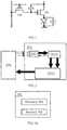
- the optical compensation system is as shown in FIG. 2 .
- a hardware environment and structure shown in FIG. 2 merely are exemplary, but not restrictive; and as required, the hardware environment may also have other components and structures, and for example, may comprise an image processing integrator and the like.
- the optical compensation system comprises a display panel 201 and an optical compensation device 202
- the optical compensation device 202 comprises a camera 2021, a data processing unit 2022 and a control unit 2023 which are in a signal connection in a wired or wireless mode.
- the AMOLED display panel may comprise a data decoding circuit, a timing controller (Tcon), a gate driving circuit, a data driving circuit, a storage apparatus (for example, a flash memory and the like) and the like, in addition to a pixel array.
- the data decoding circuit receives a display input signal and decodes the display input signal to obtain a display data signal; and the timing controller outputs a timing signal to control the gate driving circuit, the data driving circuit and the like to synchronously work, and can carry out gamma processing on the display data signal and input the processed display data signal to the data driving circuit to perform a display operation.
- the timing controller upon performing a gamma processing on the display data signal, can also simultaneously perform a compensation processing.
- the timing controller can read a pre-stored pixel compensation parameter from the storage apparatus and further process the display data signal by adopting the pixel compensation parameter to obtain the compensated display data signal. And after the timing controller completing the gamma processing and the compensation processing, outputs the display data signal to the data driving circuit for the display operation.
- the display panel also can comprise an independent gamma processing circuit which performs gamma processing, compensation processing and the like on the display data signal under the control of the timing controller.
- the optical compensation device 202 comprises a processor 301 and a memory 302.
- the memory 302 is configured to store a computer program instruction, and the computer program instruction is applicable to be loaded by the processor 301 and execute the optical compensation method for the display panel (which will be illustrated in detail later), and achieves functional effects of each functional module (for example, the data processing unit 2022 and the control unit 2023) in FIG. 2 .
- the processor 301 may be any one of various applicable processor, for example, is implemented in a form of a central processor, a microprocessor, an embedded processor and the like, and may adopt architectures of X86, ARM and the like; and the memory 302 may be any one of various applicable storage apparatus, such as a non-volatile storage apparatus, which comprise, but are not limited to a magnetic storage apparatus, a semiconductor storage apparatus, an optical storage apparatus and the like, and can be arranged in a form of a single storage apparatus, a storage apparatus array or a distributed storage apparatus, and the embodiments of the present disclosure are not limited thereto.
- a non-volatile storage apparatus which comprise, but are not limited to a magnetic storage apparatus, a semiconductor storage apparatus, an optical storage apparatus and the like, and can be arranged in a form of a single storage apparatus, a storage apparatus array or a distributed storage apparatus, and the embodiments of the present disclosure are not limited thereto.
- the optical compensation device 202 comprises a processor 301, a memory 302 and a camera 303.
- the processor 301 and the memory 302 herein have the same structure and function as the processor 301 and the memory 302 shown in FIG. 3A , and are not repeated herein.
- the camera 303 is configured to shoot a picture displayed by the display panel and send the shot picture into the processor so as to acquire display parameters of a plurality of pixels on the display panel.
- the data processing unit 2022 of the optical compensation device 202 sends out a test image to the control unit 2023, and the control unit 2023 processes the test image to acquire a pixel compensation parameter and inputs the pixel compensation parameter into the storage apparatus of the display panel 201 to store so as to drive the display panel 201 to display the image when the display panel works.
- the operation that the control unit acquires the pixel compensation parameter can comprise: acquiring pixel compensation parameters of all pixels on the display panel, and storing the pixel compensation parameters in the storage apparatus for retrieving when the display panel displays the image subsequently.
- control unit acquires pixel compensation parameters of a part of pixels on the display panel and uses the pixel compensation parameters for compensating brightness non-uniformity of the display panel in real time.
- the camera 2021 shoots to acquire brightness information of each pixel of the tested display panel 201 in a selected gray scale.
- the data processing unit 2022 processes to obtain an actual measured brightness and gray scale response curve of each pixel, and then writes a compensation multinomial coefficient into the storage apparatus in the display panel 201 under the control of the control unit 2023 on the basis of an ideal brightness and gray scale response curve according to a method for changing brightness by regulating the gray scale, e.g., a method for performing curve fitting on a gray scale after compensation and an input gray scale by using a multinomial and finally obtaining the compensation multinomial coefficient.
- the control unit e.g., the timing controller
- the control unit reads those multinomial coefficients for pixel compensation from the storage apparatus and processes to obtain a corrected gray scale of each gray scale of each pixel so as to implement real-time compensation on brightness non-uniformity of each pixel and finally alleviate brightness non-uniformity of the display panel 201.
- each pixel of the OLED display panel can be subjected to color non-uniformity compensation.
- the camera 2021 comprises, but is not limited to, a charge coupled device (CCD) camera and a complementary metal oxide semiconductor (CMOS) camera.
- CCD charge coupled device
- CMOS complementary metal oxide semiconductor
- the optical compensation method as mentioned above has the difficulty of how to accurately capture correct brightness of each pixel by the camera 2021, particularly when the structure of the display panel is not flat.
- the display panel 201 can be a curved display panel, and for example, two side edges or four side edges of the curved display panel have a shape of a circular arc, so that a narrower frame can be implemented.
- the camera 2021 cannot accurately capture correct brightness of pixels at a curved edge portion of the display panel 201, and for the pixels at the curved edge portion, a brightness value obtained by shooting is lower than actual brightness values of those portions of the display panel 201, resulting in that after the optical compensation, the display panel 201 has a phenomenon that brightness of the edge portion is higher than that of a non-edge portion.
- At least one embodiment of the present disclosure provides a flow chat of an optical compensation method for a display panel as shown in FIG. 4 .
- the method can be applied to an optical compensation device 202, and is loaded and executed by a processor 301 so as to at least solve the problem that brightness of the edge of the curved display panel is higher than that of the non-edge portion of the curved display panel after the curved display panel performing the optical compensation.
- the steps shown in the flow chat of the drawing can be executed in a computer system such as a group of computer executable instructions, and a logic sequence is shown in the flow chart, but in some cases, the shown or described steps can be executed in a different sequence.
- the method can comprise the following steps:
- the pixel block as mentioned above comprises at least one pixel, i.e., the pixel block comprises N ⁇ M pixels.
- N is an integer between 1 and 10
- M is an integer between 1 and 10.
- the pixel blocks P on the display panel are arranged along a row direction and a column direction.
- acquiring pixel compensation parameters of a plurality of pixel blocks on the display panel can comprise steps as follows.
- the OLED display panel receives a test image (e.g., a uniform gray scale image) sent out by a control unit of the optical compensation device.
- a test image e.g., a uniform gray scale image
- the picture displayed by the OLED display panel is shot by a camera; and an image of the shot display picture is sent into a data processing unit to be processed and analyzed to acquire display parameters (e.g., color or brightness and the like) of corresponding pixels of the display panel, so as to acquire the pixel compensation parameter of each pixel block of the display panel.
- picture data of the test image displayed by the display panel is acquired; on the basis of color distribution or brightness distribution of the picture data, a color difference or brightness difference between each pixel block of the display panel and each pixel block in a target test picture is identified; and according to a size of the color difference or brightness difference between each pixel block of the display panel and each pixel block in the target test picture, the display panel is partitioned into the main body region and the edge region, and the color difference or brightness difference of the edge region is greater than that of the main body region. Then, according to the color difference or brightness difference between the pixel block in the main body region and the pixel block in the target test picture, the pixel compensation parameter of the pixel block in the main body region is acquired by utilizing a compensation algorithm.
- the method of optical compensation can be performed with reference to the optical compensation device 202 in FIG. 2 .
- the picture data of the test image displayed by the display panel 201 is acquired by using the high-resolution and high-accuracy CCD camera 2021, and the CCD camera 2021 sends the picture data to the data processing unit 2022 after shooting the picture data.
- the data processing unit 2022 analyzes color distribution or brightness distribution characteristics of each pixel block of the display panel according to the acquired picture data and identifies the color difference or brightness difference (i.e., mura) between each pixel block of the display panel and each pixel block in the target test picture according to a related algorithm.
- the related algorithm includes, but is not limited to, an optical measurement method.
- the pixel compensation parameters i.e., an offset and a gain, of each pixel block of the display panel is calculated.
- the optical compensation algorithm includes, but is not limited to, a Demura compensation algorithm.
- the pixel compensation parameter of the pixel block in the main body region which is acquired by the optical compensation device 202, is used as the pixel compensation parameter of the pixel block to be compensated.
- the embodiments are not limited thereto.
- the pixel compensation parameter of the pixel block to be compensated in the edge region also can be acquired when the pixel compensation parameter of the pixel block in the main body region is acquired, and then the pixel compensation parameter of the pixel block to be compensated is regulated to be consistent with the pixel compensation parameter of the pixel block in the main body region.
- the display panel 201 comprises an edge region 501, an edge region 502, an edge region 503, an edge region 504, an edge region 505, an edge region 506, an edge region 507, an edge region 508 and a main body region 509 positioned in a plurality of edge regions.
- selecting the edge region of the display panel further can be implemented in two modes as follows:
- n rows or m columns of pixels which are inwards from a side edge are selected as the edge region
- n and m are integers greater than 1 and for example, are 5 to 15, and values of n and m can be selected based on experience or selected according to design parameters of the display panel.
- the pixel compensation parameter of the pixel block in the main body region which is the closest to the pixel block to be compensated, can be extracted from the acquired pixel compensation parameters of a plurality of pixel blocks in the main body region and used as the pixel compensation parameter of the pixel block to be compensated.
- the compensation parameter of the edge region of the curved display panel i.e., a flexible screen
- the compensation parameter of the edge region of the curved display panel can be separately controlled, so that after the curved display panel is subjected to optical compensation, uniformity of brightness of the edge region and brightness of the main body region of the curved display panel is implemented, and the afterimage can be further weakened.
- acquiring the pixel compensation parameter of at least one pixel block in the main body region as the pixel compensation parameter of the pixel block to be compensated comprises: acquiring a pixel compensation parameter of a first pixel block in the main body region, which is the closest to a second pixel block to be compensated, as a pixel compensation parameter of the second pixel block.
- the main body region 509 comprises a pixel block P2 and a pixel block P4, i.e., the first pixel blocks; and the edge region 502 comprises a pixel block P1, and the edge region 508 comprises a pixel block P3, i.e., the second pixel blocks.
- the pixel block P1 and the pixel block P2 are adjacent in the column direction (i.e., a Y direction as shown in FIG. 6 ), and the pixel block P3 and the pixel block P4 are adjacent in the row direction (i.e., an X direction as shown in FIG. 6 ).
- the pixel compensation parameters of the pixel block P2 and the pixel block P4, which have been acquired previously, can be acquired, and then the pixel compensation parameter of the pixel block P2 can be used as the pixel compensation parameter of the pixel block P1 in the edge region 502 and the pixel compensation parameter of the pixel block P4 can be used as the pixel compensation parameter of the pixel block P3 in the edge region 508, so that the pixel compensation parameter of the pixel block P1 in the edge region 502 is consistent with that of the pixel block P2 in the main body region 509, which is adjacent to the pixel block P1, and the pixel compensation parameter of the pixel block P3 in the edge region 508 is consistent with that of the pixel block P4 in the main body region 509, which is adjacent to the pixel block P3.
- Consistency of the pixel parameters herein means that the pixel compensation parameter of the pixel block in the edge region is regulated to be the same with that of the pixel block in the main body region, which is adjacent to the edge region, i.e., both the offset and the gain of the pixel block in the edge region are the same as that of the pixel block in the main body region adjacent to the edge region.
- acquiring the pixel compensation parameter of at least one pixel block in the main body region as the pixel compensation parameter of the pixel block to be compensated further comprises: determining an alignment mode of the second pixel block and the first pixel block, the alignment mode comprising row alignment or column alignment; and using the pixel compensation parameter of the second pixel block as pixel compensation parameters of a plurality of third pixel blocks to be compensated positioned in the same row or the same column with the second pixel block according to the alignment mode.
- the pixel block P1 and the pixel block P2 adjacent thereto are in column alignment (i.e., are aligned with each other in the column direction, i.e., the Y direction), and the pixel block P3 and the pixel block P4 adjacent thereto are in row alignment (i.e., are aligned with each other in the row direction, i.e., the X direction).
- the pixel compensation parameter of the pixel block P1 is used as a pixel compensation parameter of the pixel block P5, so that the pixel compensation parameter of the pixel block P5 is consistent with that of the pixel block P2.
- the pixel compensation parameter of the pixel block P3 is used as a pixel compensation parameter of the pixel block P6, so that the pixel compensation parameter of the pixel block P6 is consistent with that of the pixel block P4.
- FIG. 8A is a logic diagram of judgment on a corner region according to an embodiment of the present disclosure. As shown in FIG. 8A , before acquiring the pixel compensation parameter of at least one pixel block in the main body region as the pixel compensation parameter of the pixel block to be compensated, the method further comprises:
- the edge regions comprise the edge region 501, the edge region 503, the edge region 505 and the edge region 507, the pixel compensation parameters of the fourth pixel blocks positioned in the same corner region (which means one of the four corner regions) are all the same and are equal to the pixel compensation parameter of the first pixel block which is the closest to the corner region.
- the fourth pixel block can be subjected to weight distribution, and according to weight distribution, the compensation parameter of the fourth pixel block in the edge region is regulated.
- performing weight distribution on the fourth pixel block in the edge region comprises: for each fourth pixel block, with respect to (the second pixel block) the third pixel block in row alignment or (the second pixel block) the third pixel block in column alignment, establishing a weight distribution coordinate system, the third pixel block herein being the closest to the fourth pixel block; and according to the weight distribution coordinate system, performing weight on the fourth pixel block in the edge region.
- the fourth pixel block can be positioned in a plurality of corner regions, e.g., the edge region 501, the edge region 503, the edge region 505 and the edge region 507.
- each pixel block in the edge region 501, the edge region 503, the edge region 505 and the edge region 507 is not aligned with the pixel block in the main body region 509 in the row direction and the column direction.
- the weight distribution coordinate system as shown in FIG. 8B can be established in the corner region 503, a weight is allocated to each fourth pixel block according to the corresponding weight distribution coordinate system, and then the pixel compensation parameter of the fourth pixel block is regulated.
- a second pixel block P11 positioned in the edge region is aligned with a first pixel block P8 positioned in the main body region in the Y direction, and thus, a pixel compensation parameter of the first pixel block P8 is used as a pixel compensation parameter of the second pixel block P11.
- the pixel compensation parameter of the first pixel block P8 is used as a pixel compensation parameter of a second pixel block P10.
- a third pixel block P12 positioned in the edge region is aligned with the second pixel block P11 in the Y direction, and thus, a pixel compensation parameter of the third pixel block P12 is regulated to be equal to that of the second pixel block P11, i.e., the pixel compensation parameter of the second pixel block P11 is used as the pixel compensation parameter of the third pixel block P12.
- a pixel compensation parameter of a third pixel block P9 is regulated to be equal to that of the second pixel block P10. Therefore, the pixel compensation parameters of the second pixel block P11, the second pixel block P10, the third pixel block P12 and the third pixel block P9 are all equal to that of the first pixel block P8.
- offset and gain values of the regulated pixel compensation parameters of the third pixel block P12 respectively are 24 and 20; and offset and gain values of the regulated pixel compensation parameters of the pixel block P9 respectively are 24 and 20.
- weights corresponding to coordinate axes of the weight distribution coordinate system are sequentially and orderly changed.
- position coordinates of a fourth pixel block P13 are acquired according to a position of the fourth pixel block P13, and the position coordinates correspond to a weight distributed to the fourth pixel block P13.
- a weight allocated in the row direction is 4, and a weight allocated in the column direction is 2.
- the method further comprises: reading the pixel compensation parameter of the pixel block in the main body region of the display panel and the regulated pixel compensation parameter of the pixel block to be compensated in the edge region of the display panel; and inputting the pixel compensation parameter of the main body region and the regulated pixel compensation parameter of the edge region into the display panel so as to compensate a display operation for the display panel.
- the obtained pixel compensation parameter of the main body region and the obtained regulated pixel compensation parameter of the edge region are stored in the storage apparatus of the display panel for the display panel to retrieve when performing the display operation so as to compensate display data which is to be used for the display operation, and the compensated display data is used for the display operation.
- the pixel compensation parameters include, but are not limited to, the offset and the gain.
- the display panel in the embodiments of the present disclosure can be a flexible screen (a bendable display panel which is also called as a flexible display panel), and for example, the flexible screen can be curled and folded as required and can be relatively varied in appearance.
- the display panel also can adopt a plastic substrate, and by virtue of a thin film packaging technology, a protection film is adhered to the back of the display panel, so that the display panel becomes bendable and difficult to break.
- the flexible display panel can be very thin and be mounted on a flexible material such as plastic or a metal foil and the like.
- FIG. 9A is a plane structural schematic diagram of a display panel provided by an embodiment of the present disclosure
- FIG. 9B is a sectional structural schematic diagram of the display panel as shown in FIG. 9A
- the display panel comprises a curved screen
- the curved screen comprises a plane portion 500 positioned in the main body region and a curved surface portion 600 positioned in the edge region.
- the plane portion 500 covers the main body region
- the curved surface portion 600 covers the edge region.
- the curved surface portion can be positioned at a side edge of the display panel, and a bending direction of the curved surface portion faces one side where a base substrate of the display panel is positioned, i.e., the curved surface portion is bent along a direction opposite to a Z direction as shown in FIG. 9B .
- the compensation parameter of the curved surface portion, i.e., the edge region, included in the curved screen of the display panel can be separately controlled, so that after the display panel in the edge region is subjected to optical compensation, the display panel is relatively uniform in overall brightness, which further can be used for weakening the afterimage.
- the units illustrated as separation parts can be or also can be not physically separated, and the units as display parts can be or also can be not physical units, i.e., the units can be positioned in one place, or also can be distributed onto a plurality of network units. Part or all of units can be selected according to actual demands to fulfill the aim of the solutions of the embodiments.
- each functional unit in each embodiment of the present disclosure can be integrated into one processing unit, or each unit can separately and physically exist, or two or more units also can be integrated into one unit.
- the integrated unit not only can be implemented in a form of hardware, but also can be implemented in a form of a software functional unit.
- the integrated unit can be stored in a computer readable storage medium.
- the technical solutions of the present disclosure in essence or the part of the technical solutions, which makes contribution to the prior art, or all or part of the technical solutions can be reflected in a form of a software product, and the computer software product is stored in one storage medium and comprises a plurality of instructions for enabling one computer device (which may be a PC, a server or a network device and the like) to execute all or part of the steps in the method according to each embodiment of the present disclosure.
- the above-mentioned storage medium comprises a volatile storage medium or a non-volatile storage medium, e.g., various media capable of storing program codes, such as a U disk, a Read-Only Memory (ROM), a Random Access Memory (RAM), a mobile hard disk, a diskette or a compact disc and the like.
- a volatile storage medium e.g., various media capable of storing program codes, such as a U disk, a Read-Only Memory (ROM), a Random Access Memory (RAM), a mobile hard disk, a diskette or a compact disc and the like.
Landscapes
- Engineering & Computer Science (AREA)
- Physics & Mathematics (AREA)
- Computer Hardware Design (AREA)
- General Physics & Mathematics (AREA)
- Theoretical Computer Science (AREA)
- Control Of Indicators Other Than Cathode Ray Tubes (AREA)
- Control Of El Displays (AREA)
- Electroluminescent Light Sources (AREA)
- Controls And Circuits For Display Device (AREA)
Applications Claiming Priority (2)
| Application Number | Priority Date | Filing Date | Title |
|---|---|---|---|
| CN201810161083.0A CN110176209B (zh) | 2018-02-27 | 2018-02-27 | 用于显示面板的光学补偿方法和光学补偿设备 |
| PCT/CN2018/122378 WO2019165830A1 (fr) | 2018-02-27 | 2018-12-20 | Procédé de compensation optique destiné à être utilisé dans un écran d'affichage et dispositif de compensation optique |
Publications (2)
| Publication Number | Publication Date |
|---|---|
| EP3761299A1 true EP3761299A1 (fr) | 2021-01-06 |
| EP3761299A4 EP3761299A4 (fr) | 2022-01-26 |
Family
ID=67688854
Family Applications (1)
| Application Number | Title | Priority Date | Filing Date |
|---|---|---|---|
| EP18900565.5A Withdrawn EP3761299A4 (fr) | 2018-02-27 | 2018-12-20 | Procédé de compensation optique destiné à être utilisé dans un écran d'affichage et dispositif de compensation optique |
Country Status (5)
| Country | Link |
|---|---|
| US (1) | US11335253B2 (fr) |
| EP (1) | EP3761299A4 (fr) |
| JP (1) | JP7303120B2 (fr) |
| CN (1) | CN110176209B (fr) |
| WO (1) | WO2019165830A1 (fr) |
Families Citing this family (19)
| Publication number | Priority date | Publication date | Assignee | Title |
|---|---|---|---|---|
| KR102678900B1 (ko) * | 2019-12-04 | 2024-06-28 | 삼성디스플레이 주식회사 | 표시 모듈 및 표시 장치 제조 방법 |
| CN111477168B (zh) * | 2020-02-27 | 2021-12-28 | 京东方科技集团股份有限公司 | 显示面板的补偿方法、显示方法 |
| CN111833818B (zh) * | 2020-07-08 | 2021-12-24 | 武汉华星光电半导体显示技术有限公司 | 柔性折叠屏及其阈值电压补偿方法和补偿装置 |
| CN111798797B (zh) * | 2020-07-28 | 2022-05-13 | 合肥鑫晟光电科技有限公司 | 一种显示控制方法及装置、显示装置、介质 |
| CN112289274B (zh) * | 2020-10-28 | 2022-11-25 | 青岛信芯微电子科技股份有限公司 | 一种显示方法及装置 |
| KR102826935B1 (ko) * | 2020-11-13 | 2025-07-01 | 삼성디스플레이 주식회사 | 표시장치 |
| CN112927147B (zh) * | 2021-01-18 | 2023-12-22 | 华兴源创(成都)科技有限公司 | 显示模组的显示数据修正方法及装置、计算机设备及介质 |
| CN112950495B (zh) * | 2021-02-05 | 2024-05-14 | 苏州华兴源创科技股份有限公司 | 一种显示面板demura补偿方法、装置、设备及介质 |
| CN112992095B (zh) * | 2021-02-24 | 2022-09-23 | 福州京东方光电科技有限公司 | 一种叠屏显示面板及其制作方法、驱动方法、显示装置 |
| CN113284450B (zh) * | 2021-05-20 | 2023-11-28 | 京东方科技集团股份有限公司 | 一种显示面板边缘色偏的补偿方法及装置 |
| CN113160043B (zh) * | 2021-05-21 | 2024-07-12 | 京东方科技集团股份有限公司 | 一种柔性显示屏的mura处理方法及装置 |
| CN113284458B (zh) | 2021-05-31 | 2022-08-23 | 昆山工研院新型平板显示技术中心有限公司 | 显示面板的灰阶补偿方法 |
| US11721253B2 (en) * | 2021-10-19 | 2023-08-08 | Synaptics Incorporated | Demura processing for a display panel having multiple regions with different pixel densities |
| CN114112324B (zh) * | 2021-11-09 | 2024-04-26 | 合肥维信诺科技有限公司 | 显示屏亮度均匀性的测试方法及测试装置 |
| CN116597768B (zh) * | 2023-04-06 | 2025-11-14 | 长春希达电子技术有限公司 | 一种led显示屏边缘亮度修正方法 |
| CN117542326B (zh) * | 2023-12-11 | 2025-09-23 | Tcl华星光电技术有限公司 | 显示面板的补偿方法和显示装置 |
| KR20250150698A (ko) * | 2024-04-11 | 2025-10-21 | 삼성디스플레이 주식회사 | 표시 장치 및 이를 이용한 표시 패널의 구동 방법 |
| CN118587997A (zh) * | 2024-06-21 | 2024-09-03 | 北京奕斯伟计算技术股份有限公司 | 图像补偿装置、图像补偿方法、显示驱动器和显示器 |
| CN118629371B (zh) * | 2024-08-09 | 2024-11-08 | 深圳精智达技术股份有限公司 | 一种显示面板边缘亮度补偿的方法、相关装置及存储介质 |
Family Cites Families (33)
| Publication number | Priority date | Publication date | Assignee | Title |
|---|---|---|---|---|
| JP2005031493A (ja) * | 2003-07-08 | 2005-02-03 | Sankyo Kk | 平面型表示装置および平面型表示装置の調整方法 |
| TWI411967B (zh) * | 2006-08-11 | 2013-10-11 | Geo Semiconductor Inc | 用於顯示器幾何及色彩自動校準及校正之系統與方法 |
| JP2009075563A (ja) * | 2007-08-24 | 2009-04-09 | Canon Inc | 発光表示装置の表示方法 |
| CN101621701B (zh) * | 2009-01-04 | 2010-12-08 | 四川川大智胜软件股份有限公司 | 独立于几何校正的任意光滑曲面屏幕多投影仪显示墙色彩校正方法 |
| JP5776967B2 (ja) * | 2010-06-11 | 2015-09-09 | Nltテクノロジー株式会社 | 画像表示装置、画像表示装置の駆動方法、端末装置 |
| JP4777472B1 (ja) * | 2010-08-24 | 2011-09-21 | 株式会社イクス | 無研磨ガラスを用いた表示パネルのための画像補正データ生成システム、画像補正データ生成方法及び画像補正データ生成プログラム |
| JP2012098575A (ja) * | 2010-11-04 | 2012-05-24 | Seiko Epson Corp | 表示装置の輝度むら調整方法、表示装置及び電子機器 |
| JP6031327B2 (ja) * | 2012-10-31 | 2016-11-24 | キヤノン株式会社 | 投影システム、プロジェクタ及び制御方法 |
| KR101964458B1 (ko) * | 2012-12-10 | 2019-04-02 | 엘지디스플레이 주식회사 | 유기발광 표시장치 및 그의 열화보상방법 |
| CN103489405B (zh) * | 2013-09-30 | 2015-09-16 | 京东方科技集团股份有限公司 | 一种显示补偿方法、装置及显示补偿系统 |
| CN103559862B (zh) | 2013-11-11 | 2016-08-17 | 西安诺瓦电子科技有限公司 | Led显示屏的分区校正方法 |
| JP2015231140A (ja) * | 2014-06-05 | 2015-12-21 | キヤノン株式会社 | 画像処理装置、画像処理方法、及び、プログラム |
| TWI539433B (zh) * | 2014-08-13 | 2016-06-21 | 友達光電股份有限公司 | 曲面顯示裝置及其伽馬校正方法 |
| CN104375302B (zh) * | 2014-10-27 | 2020-09-08 | 上海中航光电子有限公司 | 一种像素结构、显示面板及其像素补偿方法 |
| KR102236561B1 (ko) * | 2014-12-31 | 2021-04-07 | 삼성디스플레이 주식회사 | 열화 보상 장치, 이를 포함하는 표시 장치 및 열화 보상 방법 |
| KR102261876B1 (ko) * | 2015-01-06 | 2021-06-07 | 삼성디스플레이 주식회사 | 표시 장치 및 그 구동 방법 |
| CN104992657B (zh) * | 2015-07-27 | 2017-09-22 | 京东方科技集团股份有限公司 | mura补偿模块和方法、显示装置和方法 |
| US10643577B2 (en) * | 2015-12-22 | 2020-05-05 | Sharp Kabushiki Kaisha | Display device |
| KR102477818B1 (ko) * | 2016-01-05 | 2022-12-19 | 삼성디스플레이 주식회사 | 표시 장치 |
| US10074066B2 (en) | 2016-01-16 | 2018-09-11 | International Business Machines Corporation | Two phase predictive approach for supply network optimization |
| KR102537463B1 (ko) * | 2016-01-20 | 2023-05-30 | 삼성디스플레이 주식회사 | 표시 패널의 얼룩 보상 장치, 이를 이용하는 표시 패널의 얼룩 보상 방법 및 이를 포함하는 표시 패널의 구동 방법 |
| CN105590604B (zh) * | 2016-03-09 | 2018-03-30 | 深圳市华星光电技术有限公司 | Mura现象补偿方法 |
| JP6744757B2 (ja) * | 2016-05-13 | 2020-08-19 | シナプティクス・ジャパン合同会社 | 画像圧縮装置、画像展開装置、画像圧縮展開システム及び表示ドライバ |
| CN106339196B (zh) * | 2016-08-31 | 2019-03-15 | 深圳市华星光电技术有限公司 | DeMura表的数据压缩、解压缩方法及Mura补偿方法 |
| CN106412549B (zh) * | 2016-10-28 | 2018-07-20 | 京东方科技集团股份有限公司 | 图像亮度调整方法及装置 |
| CN106842752B (zh) * | 2017-04-24 | 2019-06-07 | 京东方科技集团股份有限公司 | 显示面板、显示装置及其显示方法 |
| CN106952627B (zh) * | 2017-05-03 | 2019-01-15 | 深圳市华星光电技术有限公司 | 一种显示面板的mura现象补偿方法及显示面板 |
| CN106935224B (zh) * | 2017-05-12 | 2019-06-07 | 京东方科技集团股份有限公司 | 显示装置及其驱动方法和驱动电路 |
| CN107170372B (zh) * | 2017-06-26 | 2019-11-22 | 上海天马微电子有限公司 | 曲面显示面板和显示装置 |
| CN107644410B (zh) * | 2017-09-29 | 2020-05-19 | 上海天马有机发光显示技术有限公司 | 图像处理方法、图像处理装置、图像处理系统及显示装置 |
| CN107610143B (zh) * | 2017-09-29 | 2020-05-19 | 上海天马有机发光显示技术有限公司 | 图像处理方法、图像处理装置、图像处理系统及显示装置 |
| CN107644610A (zh) * | 2017-10-31 | 2018-01-30 | 昆山国显光电有限公司 | 异形显示屏和集成异形显示屏的显示装置 |
| KR102417070B1 (ko) * | 2017-11-06 | 2022-07-06 | 삼성디스플레이 주식회사 | 휘도 불균일 보상 방법 및 이를 채용한 표시 장치 |
-
2018
- 2018-02-27 CN CN201810161083.0A patent/CN110176209B/zh active Active
- 2018-12-20 US US16/480,448 patent/US11335253B2/en active Active
- 2018-12-20 WO PCT/CN2018/122378 patent/WO2019165830A1/fr not_active Ceased
- 2018-12-20 JP JP2019564145A patent/JP7303120B2/ja active Active
- 2018-12-20 EP EP18900565.5A patent/EP3761299A4/fr not_active Withdrawn
Also Published As
| Publication number | Publication date |
|---|---|
| EP3761299A4 (fr) | 2022-01-26 |
| JP7303120B2 (ja) | 2023-07-04 |
| US20210335223A1 (en) | 2021-10-28 |
| CN110176209B (zh) | 2021-01-22 |
| CN110176209A (zh) | 2019-08-27 |
| JP2021515253A (ja) | 2021-06-17 |
| US11335253B2 (en) | 2022-05-17 |
| WO2019165830A1 (fr) | 2019-09-06 |
Similar Documents
| Publication | Publication Date | Title |
|---|---|---|
| US11335253B2 (en) | Optical compensation method for display panel and optical compensation device | |
| CN109147668B (zh) | 显示面板的外部补偿方法、驱动单元及显示面板 | |
| CN110444152B (zh) | 光学补偿方法及装置、显示装置、显示方法及存储介质 | |
| CN114694617B (zh) | 用于补偿劣化的显示装置及其补偿方法 | |
| CN109389943B (zh) | 显示装置及其驱动方法 | |
| CN106373093B (zh) | 图像处理方法、图像处理电路和显示设备 | |
| CN113724652B (zh) | OLED显示面板Mura的补偿方法、装置及可读介质 | |
| US9685106B2 (en) | Method for compensating image distortion caused by the curvature of a display device | |
| US9805671B2 (en) | Curved display and a driving method thereof | |
| KR101957758B1 (ko) | 유기발광표시장치 및 그 구동방법 | |
| CN107203056B (zh) | 针对超高分辨率面板的mura处理方法 | |
| CN109949744B (zh) | 伽马电压校正方法及装置 | |
| KR102149480B1 (ko) | 표시장치의 얼룩 보상 방법 및 및 장치 | |
| US20200105190A1 (en) | Compensation method and compensation device, display apparatus, display method and storage medium | |
| US10068516B2 (en) | Display device having temperature compensation and method of driving the same | |
| US20150116384A1 (en) | Display device and compensation method for the same | |
| WO2015180371A1 (fr) | Procédé de compensation de luminosité de dispositif d'affichage, appareil de compensation de luminosité et dispositif d'affichage | |
| KR20210157953A (ko) | 표시 장치를 검사하는 검사 장치, 얼룩 보상을 수행하는 표시 장치 및 얼룩 보상 방법 | |
| US9886883B2 (en) | Display apparatus and a method of operating the same | |
| CN112365840A (zh) | 显示面板的补偿方法、装置及显示装置 | |
| US9685123B2 (en) | Method of testing a display apparatus and a display apparatus tested by the same | |
| KR102295195B1 (ko) | 표시장치의 얼룩 보상 방법 및 및 장치 | |
| CN108735776B (zh) | 一种像素排列 | |
| TWI603314B (zh) | 顯示器的控制方法 | |
| US10056049B2 (en) | Display apparatus and method of operating the same |
Legal Events
| Date | Code | Title | Description |
|---|---|---|---|
| STAA | Information on the status of an ep patent application or granted ep patent |
Free format text: STATUS: UNKNOWN |
|
| STAA | Information on the status of an ep patent application or granted ep patent |
Free format text: STATUS: THE INTERNATIONAL PUBLICATION HAS BEEN MADE |
|
| PUAI | Public reference made under article 153(3) epc to a published international application that has entered the european phase |
Free format text: ORIGINAL CODE: 0009012 |
|
| STAA | Information on the status of an ep patent application or granted ep patent |
Free format text: STATUS: REQUEST FOR EXAMINATION WAS MADE |
|
| 17P | Request for examination filed |
Effective date: 20190723 |
|
| AK | Designated contracting states |
Kind code of ref document: A1 Designated state(s): AL AT BE BG CH CY CZ DE DK EE ES FI FR GB GR HR HU IE IS IT LI LT LU LV MC MK MT NL NO PL PT RO RS SE SI SK SM TR |
|
| AX | Request for extension of the european patent |
Extension state: BA ME |
|
| DAV | Request for validation of the european patent (deleted) | ||
| DAX | Request for extension of the european patent (deleted) | ||
| A4 | Supplementary search report drawn up and despatched |
Effective date: 20220104 |
|
| RIC1 | Information provided on ipc code assigned before grant |
Ipc: G09G 5/10 20060101ALI20211221BHEP Ipc: G09G 3/3208 20160101AFI20211221BHEP |
|
| STAA | Information on the status of an ep patent application or granted ep patent |
Free format text: STATUS: THE APPLICATION HAS BEEN WITHDRAWN |
|
| 18W | Application withdrawn |
Effective date: 20241107 |