EP3761359B1 - Ensemble de cadre de plomb pour dispositif semi-conducteur - Google Patents
Ensemble de cadre de plomb pour dispositif semi-conducteur Download PDFInfo
- Publication number
- EP3761359B1 EP3761359B1 EP19184250.9A EP19184250A EP3761359B1 EP 3761359 B1 EP3761359 B1 EP 3761359B1 EP 19184250 A EP19184250 A EP 19184250A EP 3761359 B1 EP3761359 B1 EP 3761359B1
- Authority
- EP
- European Patent Office
- Prior art keywords
- die
- lead
- lead portion
- connection portion
- continuous
- Prior art date
- Legal status (The legal status is an assumption and is not a legal conclusion. Google has not performed a legal analysis and makes no representation as to the accuracy of the status listed.)
- Active
Links
Images

Classifications
-
- H—ELECTRICITY
- H10—SEMICONDUCTOR DEVICES; ELECTRIC SOLID-STATE DEVICES NOT OTHERWISE PROVIDED FOR
- H10W—GENERIC PACKAGES, INTERCONNECTIONS, CONNECTORS OR OTHER CONSTRUCTIONAL DETAILS OF DEVICES COVERED BY CLASS H10
- H10W70/00—Package substrates; Interposers; Redistribution layers [RDL]
- H10W70/40—Leadframes
- H10W70/421—Shapes or dispositions
-
- H—ELECTRICITY
- H10—SEMICONDUCTOR DEVICES; ELECTRIC SOLID-STATE DEVICES NOT OTHERWISE PROVIDED FOR
- H10W—GENERIC PACKAGES, INTERCONNECTIONS, CONNECTORS OR OTHER CONSTRUCTIONAL DETAILS OF DEVICES COVERED BY CLASS H10
- H10W70/00—Package substrates; Interposers; Redistribution layers [RDL]
- H10W70/40—Leadframes
- H10W70/421—Shapes or dispositions
- H10W70/424—Cross-sectional shapes
- H10W70/427—Bent parts
- H10W70/429—Bent parts being the outer leads
-
- H—ELECTRICITY
- H10—SEMICONDUCTOR DEVICES; ELECTRIC SOLID-STATE DEVICES NOT OTHERWISE PROVIDED FOR
- H10W—GENERIC PACKAGES, INTERCONNECTIONS, CONNECTORS OR OTHER CONSTRUCTIONAL DETAILS OF DEVICES COVERED BY CLASS H10
- H10W70/00—Package substrates; Interposers; Redistribution layers [RDL]
- H10W70/40—Leadframes
- H10W70/464—Additional interconnections in combination with leadframes
- H10W70/466—Tape carriers or flat leads
-
- H—ELECTRICITY
- H10—SEMICONDUCTOR DEVICES; ELECTRIC SOLID-STATE DEVICES NOT OTHERWISE PROVIDED FOR
- H10W—GENERIC PACKAGES, INTERCONNECTIONS, CONNECTORS OR OTHER CONSTRUCTIONAL DETAILS OF DEVICES COVERED BY CLASS H10
- H10W70/00—Package substrates; Interposers; Redistribution layers [RDL]
- H10W70/40—Leadframes
- H10W70/481—Leadframes for devices being provided for in groups H10D8/00 - H10D48/00
-
- H—ELECTRICITY
- H10—SEMICONDUCTOR DEVICES; ELECTRIC SOLID-STATE DEVICES NOT OTHERWISE PROVIDED FOR
- H10W—GENERIC PACKAGES, INTERCONNECTIONS, CONNECTORS OR OTHER CONSTRUCTIONAL DETAILS OF DEVICES COVERED BY CLASS H10
- H10W74/00—Encapsulations, e.g. protective coatings
- H10W74/10—Encapsulations, e.g. protective coatings characterised by their shape or disposition
- H10W74/111—Encapsulations, e.g. protective coatings characterised by their shape or disposition the semiconductor body being completely enclosed
-
- H—ELECTRICITY
- H10—SEMICONDUCTOR DEVICES; ELECTRIC SOLID-STATE DEVICES NOT OTHERWISE PROVIDED FOR
- H10W—GENERIC PACKAGES, INTERCONNECTIONS, CONNECTORS OR OTHER CONSTRUCTIONAL DETAILS OF DEVICES COVERED BY CLASS H10
- H10W95/00—Packaging processes not covered by the other groups of this subclass
-
- H—ELECTRICITY
- H10—SEMICONDUCTOR DEVICES; ELECTRIC SOLID-STATE DEVICES NOT OTHERWISE PROVIDED FOR
- H10W—GENERIC PACKAGES, INTERCONNECTIONS, CONNECTORS OR OTHER CONSTRUCTIONAL DETAILS OF DEVICES COVERED BY CLASS H10
- H10W72/00—Interconnections or connectors in packages
- H10W72/90—Bond pads, in general
- H10W72/921—Structures or relative sizes of bond pads
- H10W72/926—Multiple bond pads having different sizes
-
- H—ELECTRICITY
- H10—SEMICONDUCTOR DEVICES; ELECTRIC SOLID-STATE DEVICES NOT OTHERWISE PROVIDED FOR
- H10W—GENERIC PACKAGES, INTERCONNECTIONS, CONNECTORS OR OTHER CONSTRUCTIONAL DETAILS OF DEVICES COVERED BY CLASS H10
- H10W74/00—Encapsulations, e.g. protective coatings
-
- H—ELECTRICITY
- H10—SEMICONDUCTOR DEVICES; ELECTRIC SOLID-STATE DEVICES NOT OTHERWISE PROVIDED FOR
- H10W—GENERIC PACKAGES, INTERCONNECTIONS, CONNECTORS OR OTHER CONSTRUCTIONAL DETAILS OF DEVICES COVERED BY CLASS H10
- H10W90/00—Package configurations
- H10W90/701—Package configurations characterised by the relative positions of pads or connectors relative to package parts
- H10W90/751—Package configurations characterised by the relative positions of pads or connectors relative to package parts of bond wires
- H10W90/756—Package configurations characterised by the relative positions of pads or connectors relative to package parts of bond wires between a chip and a stacked lead frame, conducting package substrate or heat sink
-
- H—ELECTRICITY
- H10—SEMICONDUCTOR DEVICES; ELECTRIC SOLID-STATE DEVICES NOT OTHERWISE PROVIDED FOR
- H10W—GENERIC PACKAGES, INTERCONNECTIONS, CONNECTORS OR OTHER CONSTRUCTIONAL DETAILS OF DEVICES COVERED BY CLASS H10
- H10W90/00—Package configurations
- H10W90/701—Package configurations characterised by the relative positions of pads or connectors relative to package parts
- H10W90/761—Package configurations characterised by the relative positions of pads or connectors relative to package parts of strap connectors
- H10W90/766—Package configurations characterised by the relative positions of pads or connectors relative to package parts of strap connectors between a chip and a stacked lead frame, conducting package substrate or heat sink
Definitions
- the present disclosure relates to a lead frame assembly for a semiconductor device.
- the present disclosure relates a clip frame structure for a semiconductor device, a semiconductor device comprising the same and an associated method of manufacturing the semiconductor device.
- clip bonded packages are commonly used as lead frame arrangements to make connections from a semiconductor die to external contacts of the device.
- Clip bonded packages have a number of advantages over conventional wire bonded packages. For example, clip bonded packages are typically used for mechanically robust and reliable electrical connections to and from the semiconductor die in automotive applications.
- the conductive clip material may have increased thermal mass compared to the wire bond material and can thus act as a heat sink for the semiconductor die.
- semiconductor device 100 comprises a semiconductor die 104 mounted on a die pad 106.
- a clip member 102 electrically connects contact terminals on a top surface of the semiconductor die 104 to external leads 108.
- the clip member is electrically connected to and mechanically bonded to the external leads 108 using a solder connection 110.
- This solder connection 110 results in increased connection resistance which can result in increased device resistance.
- the clip member is a source connection
- the increased resistance may result in increased drain-source on resistance, R dson .
- aspects of the present disclosure involve semiconductor devices comprising improved lead frame arrangements and a method of manufacturing such semiconductor devices.
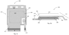
- the semiconductor device 200 prior to moulding and comprising a lead frame assembly 202 according to an embodiment is illustrated in Figures 2a and 2b .
- the semiconductor device 200 generally comprises a die attach structure 204 and a clip frame structure 206, forming the lead frame assembly 202, and a semiconductor die 208 attached to both the die attach structure 204 and the clip frame structure 206.
- the die attach structure 204 is typically arranged for mounting a semiconductor die 208 thereon and providing support for the clip frame structure 206.
- the die attach structure 204 may, depending on the arrangement of contact terminals, such as source, gate or drain, of semiconductor die 208, provide contact to a back-side or bottom contact of the semiconductor die 208.
- the die attach structure 204 is typically formed of a metallic conductive material, such as copper.
- the die attach structure 204 may provide a bottom external lead 203, such as a drain contact or tab, to a back-side or bottom contact terminal arranged on the semiconductor die 208.
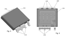
- the bottom external lead 203 may extend outside of the moulded package material of the semiconductor device 200 to form a heat sink tab to the bottom of the semiconductor die 208, as illustrated for example in Figure 5 .
- the semiconductor die 208 is fixedly arranged on the die attach structure 204, and the clip frame structure 206 is fixedly connected to the semiconductor die 208 and the die attach structure 204.
- the clip frame structure 206 is formed of two distinct but integrally formed parts, namely: a die connection portion 210; and a lead portion 212.
- the die connection portion 210 may be generally rectangular in shape and/or may be dimensioned such that it substantially corresponds to the dimensions of a contact terminal on the top side of the semiconductor die 208 to which the die connection portion 210 is attached.
- the bottom or backside contact terminal of the semiconductor die 208 may be fixedly attached to the die attach structure 204.
- the semiconductor die 208 may be fixedly attached to and may be electrically connected, via a bottom contact terminal (not illustrated) to the die attach structure 204 using any suitable bonding material such as a solder or a conductive adhesive.
- the die connection portion of the clip frame structure 206 is fixedly attached to the contact terminal arranged on a top side of the semiconductor die 208, using an appropriate bonding material, such as for example, a solder or a conductive adhesive.
- the lead portion 212 is a continuous and merged section extending from the die connection portion 210.
- the lead portion 212 is continuous in that forms a substantially elongate member extending away from and along the width of the die connection portion 210. In this way, the lead portion 212 has a continuous width W and may be seen as a merged member, that is without bifurcation or plurality of finger like lead members, which extends substantially along the width of the die connection portion 210.
- the lead portion 212 is arranged as a so-called "gull wing" lead having one or more angles or bends to allow the lead portion to contact the PCB.
- the lead portion 212 being continuous and merged may be arranged as a plate like member having the appropriate gull-wing bends formed therein.
- the lead portion 212 can be dimensioned such that it aligns or corresponds to the footprint of the contacts on a PCB (not illustrated).
- W width
- the lead portion 212 can be dimensioned such that it aligns or corresponds to the footprint of the contacts on a PCB (not illustrated).
- the lead portion By arranging the lead portion in this way it is possible to reduce the package resistance of the lead frame assembly 202 and thus reduce the operating resistance, such as Rdson, of the semiconductor device 200.
- the above arrangement does not significantly increase the inductance of the lead frame assembly 202.
- the resistance of the clip frame structure may be 0.34717 m ⁇ with an inductance of 1.9718 nH.
- the resistance of the clip frame structure may be 0.49792 m ⁇ with an inductance of 1.9898 nH.
- the semiconductor die 208 and the clip frame structure 206 is then encapsulated using a moulding material 216 (as illustrated for example in Figure 5 ) .
- the lead portion 212 and the bottom external lead 203 project through the mould compound 216 to allow the lead portion 212 and the bottom external lead 203 to contact an external carrier such as a PCB.
- the clip frame structure 206 is typically formed from a single unitary sheet of metal, such as copper, which is formed or stamped to produce the desired structure. In this way the thickness of the die connection portion 210 and a lead portion 212 of the clip frame structure 206 may be equal.
- the choice of metal is entirely at the choice of the skilled person and may be chosen dependent on the required electrical characteristics of the lead frame assembly for the semiconductor device 200.
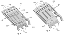
- Figures 3 and 4 illustrate a further embodiment of the lead frame assembly 202. Consistent with the arrangement described above with respect to Figures 2a and 2b , the arrangement of Figures 3 and 4 includes generally comprises a die attach structure 204 and a clip frame structure 206, forming the lead frame assembly 202, and a semiconductor die 208 attached to both the die attach structure 204 and the clip frame structure 206.
- the arrangement of Figures 3 and 4 also includes a number of first slots or holes 220 formed through the continuous lead portion (212) and the bottom external lead 203.
- the slots or holes 220 act as anchor or locking points for the mould compound 216 and allow for improved adhesion or attachment of the mould compound 216 to the lead frame assembly 202. Improved adhesion of mould compound prevents can reduce stress and package cracking during lead forming, that is cutting and bending of the die connection portion 210 and or the bottom external lead 203 post moulding.
- Second slots or holes 221 formed through the die connection portion 210 traverse or extend lengthways across the die connection portion 210. This allows for both stress relief and solder protection.
- the holes or slots 221 formed in the die connection portion 210 reduce stress spreading across the surface of the die connection portion 210 as it is fixed to the terminal arranged on the top surface of the semiconductor die. In other words the holes or slots 221 distort the stress induced the die connection portion 210 so stress does not propagate across the die connection portion 210. In terms of solder protection, the holes or slots 221 allow for gasses to escape from under the die connection portion 210 during solder reflow processes.
- Third slots or holes 222 are also incorporated in the continuous lead portion 212 to prevent the leads from springing back, due to the elastic return of the metal after formation of the leads. This also makes the leads more flexible during board level temperature cycling which can prevent the solder joints of the leads to the PCB from breaking or cracking.
- the arrangement of Figures 3, 4 and 5 also illustrate one or more optional lead end portions 224 arranged at one end of the lead portion 212 distal to the die connection portion 210.
- the lead end portions 224 and the lead portion 212 may comprise one or more bends 230 intermediate the die connection portion 210 and an extremity of the lead end portions 224, such that the leads are formed as so-called "gull wing" leads.
- the lead end portions 224 may be arranged in any standard lead geometry as required by the footprint of the contacts on a PCB.
- the lead geometry may be the Small Outline Integrated Circuit (SOIC) such as SO8, SO14, SO16 or any other appropriate package outline.
- SOIC Small Outline Integrated Circuit
- clip frame structure 206 may form a source connection to a source terminal on top side of the semiconductor die 208.
- a lead 218 may form a gate connection to a gate terminal also formed on the top side of the semiconductor die 208.
- the bottom external lead 203 may form a drain connection to a drain terminal formed on the back side of the semiconductor die 106.
- the semiconductor die 106 may be a field effect transistor.
- the semiconductor die 208 may be a bipolar junction transistor.
- the clip frame structure 206 may form a collector connection to a collector terminal on the top side of the semiconductor die 208.
- the lead 218 may form a base connection to a base terminal also formed on the top side of the semiconductor die 208.
- the bottom external lead 203 may form an emitter connection to an emitter terminal formed on the back side of the semiconductor die 208.
- Figure 6 illustrates the slots or holes 220 arranged in the bottom external lead 203 anchoring the mould compound 216 to the bottom external lead 203 so as to allow for improved adhesion or attachment of the mould compound 216 to the bottom external lead 203.
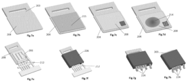
- Figures 7a to 7h illustrate the process flow steps for manufacturing a semiconductor device according to embodiments.
- the die attach structure 204 with a bottom external lead 203 extending therefrom is provided.
- the die attach structure 204 and bottom external lead 203 may be formed of any appropriate conductive material such as copper.
- the arrangement of Figure 7a shows a single die attach structure 204, however the skilled person will appreciate that a plurality of die attach structures may be arranged in a strip or matrix.
- a die attach material 215 is dispensed onto the die attach structure 204.
- the die attach material 215 is arranged for fixedly mounting the semiconductor die 208 to the die attach material 215, as illustrated in Figure 7c .
- the die attach material 215 may be any appropriate adhesive material such as a solder or conductive adhesive.
- a contact terminal attach material is dispended on the top side contact of the semiconductor die 208 for electrical and mechanical connection of the clip frame structure 206 to the semiconductor die 208 as illustrated in Figure 7d .
- the die attach material may be applied by any appropriate process such as adhesive or solder printing or dispense.
- the contact terminal attach material 214 is arranged on the one or more top contacts of the semiconductor die 208.
- the clip frame structure 206 may then be arranged on the contact terminals, as illustrated in Figure 7e . Whilst the arrangement of Figure 7e illustrates a single clip frame structure 206 arranged on the semiconductor die 208, the skilled person will appreciate that a plurality of such clip frame structures may be arranged in a strip or matrix corresponding to the plurality of die attach structures each having a semiconductor die arranged thereon. Following connection of the clip frame structure 206 the assembly undergoes solder re-flow to solidify the die attach material and the contact terminal attach material. Following re-flow, the assembly may be packaged in a mould material 216 as illustrated in Figure 7f .
- the lead end portions 224 are formed by trimming the lead portion 212 and bending the leads to form the gull-wing arrangement.
- the process is completed in Figure 7h by trimming of the bottom external lead 203.
Landscapes
- Lead Frames For Integrated Circuits (AREA)
- Structures Or Materials For Encapsulating Or Coating Semiconductor Devices Or Solid State Devices (AREA)
Claims (6)
- Ensemble grille de connexion destiné à un dispositif semi-conducteur, l'ensemble grille de connexion comprenant :
une structure de fixation de puce (204) et une structure de cadre de pince (206), la structure de cadre de pince comprenant :une partie de raccordement de puce (210) conçue pour venir en contact avec une borne de contact sur un côté supérieur de la puce semi-conductrice (208) ; et une partie conducteur continu (212) s'étendant le long de la partie de raccordement de puce (210) ;la partie conducteur continu (212) étant formée d'un seul tenant avec la partie de raccordement de puce (210) ;la partie conducteur continu (212) étant une partie conducteur fusionné qui s'étend sensiblement à travers la largeur de la partie de raccordement de puce (210),la partie de raccordement de puce (210) comprenant un deuxième trou ou des deuxièmes trous (221) transversaux ou s'étendant longitudinalement à travers la partie de raccordement de puce (210),caractérisé en ce que la partie conducteur continu (212) comprend un ou plusieurs premiers trous ou une ou plusieurs premières fentes (220) conçus pour servir de points d'ancrage ou de verrouillage pour un composé de moule, et la partie conducteur continu (212) comprend un ou plusieurs troisièmes trous ou une ou plusieurs troisièmes fentes (222) conçus pour éviter que la partie conducteur continu (212) ne revienne en arrière. - Ensemble grille de connexion selon la revendication 1, dans lequel la partie conducteur continu comprend un ou plusieurs coudes en son sein conçus et agencés pour permettre à la partie conducteur de venir en contact avec un support.
- Ensemble grille de connexion selon les revendications 1 à 2, dans lequel la partie conducteur continu comprend en outre une pluralité d'extrémités de conducteur.
- Dispositif semi-conducteur, comprenant l'ensemble grille de connexion selon les revendications 1 à 3, ayant un dispositif de puce semi-conductrice monté sur la structure de fixation de puce.
- Procédé de fabrication d'un dispositif semi-conducteur, le procédé comprenant les étapes suivantes consistant à :fournir un ensemble grille de connexion ;monter une puce semi-conductrice (208) sur une structure de fixation de puce (204) de l'ensemble grille de connexion ;fournir une structure de cadre de pince, la structure de cadre de pince comprenant :une partie de raccordement de puce (210) conçue pour venir en contact avec une borne de contact sur un côté supérieur de la puce semi-conductrice (208) ; etune partie conducteur continu (212) s'étendant le long de la partie de raccordement de puce ; la partie conducteur continu (212) étant formée d'un seul tenant avec la partie de raccordement de puce (210) ;la partie conducteur continu (212) étant une partie conducteur fusionné et étant formée pour s'étendre sensiblement à travers la largeur de la partie de raccordement de puce (210) ;fournir en outre au sein de la partie conducteur continu (212) un ou plusieurs premiers trous ou une ou plusieurs premières fentes (220) conçus pour servir de points d'ancrage ou de verrouillage pour un composé de moule ;fournir en outre au sein de la partie de raccordement de puce (210) un deuxième trou ou des deuxièmes trous (221) transversaux ou s'étendant longitudinalement à travers la partie de raccordement de puce (210) ;fournir en outre au sein de la partie conducteur continu (212) un ou plusieurs troisièmes trous ou une ou plusieurs troisièmes fentes (222) conçus pour éviter que la partie conducteur continu (212) ne revienne en arrière.
- Procédé selon la revendication 5, formant un ou plusieurs coudes dans la partie conducteur continu pour permettre à la partie conducteur de venir en contact avec un support.
Priority Applications (5)
| Application Number | Priority Date | Filing Date | Title |
|---|---|---|---|
| EP19184250.9A EP3761359B1 (fr) | 2019-07-03 | 2019-07-03 | Ensemble de cadre de plomb pour dispositif semi-conducteur |
| US16/919,426 US11973009B2 (en) | 2019-07-03 | 2020-07-02 | Lead frame assembly for a semiconductor device |
| CN202010630833.1A CN112185923A (zh) | 2019-07-03 | 2020-07-03 | 半导体装置的引线框架组件 |
| CN202511765381.7A CN121568581A (zh) | 2019-07-03 | 2020-07-03 | 半导体装置的引线框架组件 |
| US18/631,535 US20240258207A1 (en) | 2019-07-03 | 2024-04-10 | Lead frame assembly for a semiconductor device |
Applications Claiming Priority (1)
| Application Number | Priority Date | Filing Date | Title |
|---|---|---|---|
| EP19184250.9A EP3761359B1 (fr) | 2019-07-03 | 2019-07-03 | Ensemble de cadre de plomb pour dispositif semi-conducteur |
Publications (2)
| Publication Number | Publication Date |
|---|---|
| EP3761359A1 EP3761359A1 (fr) | 2021-01-06 |
| EP3761359B1 true EP3761359B1 (fr) | 2025-04-30 |
Family
ID=67184786
Family Applications (1)
| Application Number | Title | Priority Date | Filing Date |
|---|---|---|---|
| EP19184250.9A Active EP3761359B1 (fr) | 2019-07-03 | 2019-07-03 | Ensemble de cadre de plomb pour dispositif semi-conducteur |
Country Status (3)
| Country | Link |
|---|---|
| US (2) | US11973009B2 (fr) |
| EP (1) | EP3761359B1 (fr) |
| CN (2) | CN112185923A (fr) |
Families Citing this family (8)
| Publication number | Priority date | Publication date | Assignee | Title |
|---|---|---|---|---|
| EP3996129A1 (fr) * | 2020-11-04 | 2022-05-11 | Nexperia B.V. | Dispositif à semi-conducteur et procédé de fabrication d'un dispositif à semi-conducteur |
| IT202100017207A1 (it) | 2021-06-30 | 2022-12-30 | St Microelectronics Srl | Procedimento per fabbricare dispositivi a semiconduttore e dispositivo a semiconduttore corrispondente |
| CN218123353U (zh) * | 2021-06-30 | 2022-12-23 | 意法半导体股份有限公司 | 半导体器件 |
| EP4184571A1 (fr) * | 2021-11-18 | 2023-05-24 | Nexperia B.V. | Boîtier à semi-conducteurs ayant une connexion améliorée des broches aux plots de liaison de la moule à semiconducteur |
| CN117766498A (zh) * | 2022-09-16 | 2024-03-26 | 力特半导体(无锡)有限公司 | 不对称瞬态电压抑制器的封装结构 |
| US12635555B2 (en) * | 2023-03-17 | 2026-05-19 | Semiconductor Components Industries, Llc | Full AG sinter discrete premium package |
| JP2026524383A (ja) * | 2023-06-27 | 2026-07-22 | テスラ,インコーポレイテッド | 方向ロック構造を有する半導体パッケージ |
| US20250132231A1 (en) * | 2023-10-19 | 2025-04-24 | Semiconductor Components Industries, Llc | Slotted clips for reduction of molding compound delamination |
Citations (8)
| Publication number | Priority date | Publication date | Assignee | Title |
|---|---|---|---|---|
| JPH04370961A (ja) * | 1991-06-19 | 1992-12-24 | Rohm Co Ltd | 電子部品の製造に使用するリードフレームの構造 |
| US6075286A (en) * | 1997-06-02 | 2000-06-13 | International Rectifier Corporation | Stress clip design |
| US6707138B2 (en) * | 1999-12-01 | 2004-03-16 | Amkor Technology, Inc. | Semiconductor device including metal strap electrically coupled between semiconductor die and metal leadframe |
| US20100109135A1 (en) * | 2008-11-06 | 2010-05-06 | Jereza Armand Vincent C | Semiconductor die package including lead with end portion |
| US20130147064A1 (en) * | 2008-09-10 | 2013-06-13 | Renesas Electronics Corporation | Semiconductor device |
| US20150262917A1 (en) * | 2014-03-12 | 2015-09-17 | Kabushiki Kaisha Toshiba | Semiconductor device and method of manufacturing the same |
| US20160293523A1 (en) * | 2015-03-31 | 2016-10-06 | Stmicroelectronics, Inc. | Semiconductor device including conductive clip with flexible leads and related methods |
| US20190131216A1 (en) * | 2017-10-30 | 2019-05-02 | Microchip Technology Incorporated | Integrated Circuit (IC) Die Attached Between An Offset Lead Frame Die-Attach Pad And A Discrete Die-Attach Pad |
Family Cites Families (22)
| Publication number | Priority date | Publication date | Assignee | Title |
|---|---|---|---|---|
| JP2959521B2 (ja) * | 1997-05-21 | 1999-10-06 | 日本電気株式会社 | 半導体装置の製造方法、リードフレーム |
| KR20000057810A (ko) * | 1999-01-28 | 2000-09-25 | 가나이 쓰토무 | 반도체 장치 |
| US6307755B1 (en) * | 1999-05-27 | 2001-10-23 | Richard K. Williams | Surface mount semiconductor package, die-leadframe combination and leadframe therefor and method of mounting leadframes to surfaces of semiconductor die |
| US6762067B1 (en) * | 2000-01-18 | 2004-07-13 | Fairchild Semiconductor Corporation | Method of packaging a plurality of devices utilizing a plurality of lead frames coupled together by rails |
| US6469398B1 (en) * | 2001-03-29 | 2002-10-22 | Kabushiki Kaisha Toshiba | Semiconductor package and manufacturing method thereof |
| US20040080028A1 (en) * | 2002-09-05 | 2004-04-29 | Kabushiki Kaisha Toshiba | Semiconductor device with semiconductor chip mounted in package |
| US6867481B2 (en) * | 2003-04-11 | 2005-03-15 | Fairchild Semiconductor Corporation | Lead frame structure with aperture or groove for flip chip in a leaded molded package |
| US20050224925A1 (en) * | 2004-04-01 | 2005-10-13 | Peter Chou | Lead frame having a tilt flap for locking molding compound and semiconductor device having the same |
| US7557432B2 (en) * | 2005-03-30 | 2009-07-07 | Stats Chippac Ltd. | Thermally enhanced power semiconductor package system |
| US7285849B2 (en) * | 2005-11-18 | 2007-10-23 | Fairchild Semiconductor Corporation | Semiconductor die package using leadframe and clip and method of manufacturing |
| JP4450230B2 (ja) * | 2005-12-26 | 2010-04-14 | 株式会社デンソー | 半導体装置 |
| US20090057852A1 (en) * | 2007-08-27 | 2009-03-05 | Madrid Ruben P | Thermally enhanced thin semiconductor package |
| DE102006015447B4 (de) * | 2006-03-31 | 2012-08-16 | Infineon Technologies Ag | Leistungshalbleiterbauelement mit einem Leistungshalbleiterchip und Verfahren zur Herstellung desselben |
| US8106501B2 (en) * | 2008-12-12 | 2012-01-31 | Fairchild Semiconductor Corporation | Semiconductor die package including low stress configuration |
| JP5090088B2 (ja) * | 2007-07-05 | 2012-12-05 | ルネサスエレクトロニクス株式会社 | 半導体装置およびその製造方法 |
| US8222718B2 (en) * | 2009-02-05 | 2012-07-17 | Fairchild Semiconductor Corporation | Semiconductor die package and method for making the same |
| US8581376B2 (en) * | 2010-03-18 | 2013-11-12 | Alpha & Omega Semiconductor Incorporated | Stacked dual chip package and method of fabrication |
| KR101249745B1 (ko) * | 2011-05-16 | 2013-04-03 | 제엠제코(주) | 반도체 패키지용 클립, 이를 이용한 반도체 패키지 및 그 제조방법 |
| US9018744B2 (en) * | 2012-09-25 | 2015-04-28 | Infineon Technologies Ag | Semiconductor device having a clip contact |
| US8981539B2 (en) * | 2013-06-10 | 2015-03-17 | Alpha & Omega Semiconductor, Inc. | Packaged power semiconductor with interconnection of dies and metal clips on lead frame |
| KR20160033870A (ko) * | 2014-09-18 | 2016-03-29 | 제엠제코(주) | 클립 구조체를 이용한 반도체 패키지 |
| CN109643957B (zh) * | 2016-08-30 | 2020-12-11 | 松下半导体解决方案株式会社 | 开关电源装置以及半导体装置 |
-
2019
- 2019-07-03 EP EP19184250.9A patent/EP3761359B1/fr active Active
-
2020
- 2020-07-02 US US16/919,426 patent/US11973009B2/en active Active
- 2020-07-03 CN CN202010630833.1A patent/CN112185923A/zh active Pending
- 2020-07-03 CN CN202511765381.7A patent/CN121568581A/zh active Pending
-
2024
- 2024-04-10 US US18/631,535 patent/US20240258207A1/en active Pending
Patent Citations (8)
| Publication number | Priority date | Publication date | Assignee | Title |
|---|---|---|---|---|
| JPH04370961A (ja) * | 1991-06-19 | 1992-12-24 | Rohm Co Ltd | 電子部品の製造に使用するリードフレームの構造 |
| US6075286A (en) * | 1997-06-02 | 2000-06-13 | International Rectifier Corporation | Stress clip design |
| US6707138B2 (en) * | 1999-12-01 | 2004-03-16 | Amkor Technology, Inc. | Semiconductor device including metal strap electrically coupled between semiconductor die and metal leadframe |
| US20130147064A1 (en) * | 2008-09-10 | 2013-06-13 | Renesas Electronics Corporation | Semiconductor device |
| US20100109135A1 (en) * | 2008-11-06 | 2010-05-06 | Jereza Armand Vincent C | Semiconductor die package including lead with end portion |
| US20150262917A1 (en) * | 2014-03-12 | 2015-09-17 | Kabushiki Kaisha Toshiba | Semiconductor device and method of manufacturing the same |
| US20160293523A1 (en) * | 2015-03-31 | 2016-10-06 | Stmicroelectronics, Inc. | Semiconductor device including conductive clip with flexible leads and related methods |
| US20190131216A1 (en) * | 2017-10-30 | 2019-05-02 | Microchip Technology Incorporated | Integrated Circuit (IC) Die Attached Between An Offset Lead Frame Die-Attach Pad And A Discrete Die-Attach Pad |
Also Published As
| Publication number | Publication date |
|---|---|
| CN112185923A (zh) | 2021-01-05 |
| US11973009B2 (en) | 2024-04-30 |
| US20210005538A1 (en) | 2021-01-07 |
| EP3761359A1 (fr) | 2021-01-06 |
| US20240258207A1 (en) | 2024-08-01 |
| CN121568581A (zh) | 2026-02-24 |
Similar Documents
| Publication | Publication Date | Title |
|---|---|---|
| US20240258207A1 (en) | Lead frame assembly for a semiconductor device | |
| US6624522B2 (en) | Chip scale surface mounted device and process of manufacture | |
| KR860000410B1 (ko) | 반도체장치 및 그 조립방법 | |
| US6479888B1 (en) | Semiconductor device and a method of manufacturing the same | |
| CN100359681C (zh) | 半导体装置 | |
| CN101685810B (zh) | 用于半导体组件封装的夹片及半导体封装结构和封装方法 | |
| USRE41559E1 (en) | Semiconductor device package with improved cooling | |
| US7495323B2 (en) | Semiconductor package structure having multiple heat dissipation paths and method of manufacture | |
| CN102272922B (zh) | 具有夹互连的半导体管芯封装 | |
| US7541681B2 (en) | Interconnection structure, electronic component and method of manufacturing the same | |
| US7935575B2 (en) | Method of forming a semiconductor package and structure therefor | |
| CN112913009B (zh) | 半导体装置以及引线框材料 | |
| US20070045785A1 (en) | Reversible-multiple footprint package and method of manufacturing | |
| EP3584832A1 (fr) | Ensemble de cadres conducteurs pour dispositif semi-conducteur | |
| CN101416311A (zh) | 无夹片和无引线半导体管芯封装及其制造方法 | |
| KR100804341B1 (ko) | 반도체장치 및 그 제조방법 | |
| US7566967B2 (en) | Semiconductor package structure for vertical mount and method | |
| US20020066963A1 (en) | Ball-less clip bonding | |
| CN114520203A (zh) | 用于半导体器件封装的接触夹 | |
| JPH11191561A (ja) | 半導体装置の製造方法 | |
| US20110163432A1 (en) | Semiconductor device and method of manufacturing the same | |
| JP3942500B2 (ja) | 半導体装置の製造方法 | |
| JPS61279141A (ja) | 可撓性テ−パリ−ドを有したリ−ドフレ−ムと機械的ダイ支持体の直接接続装置及び方法 | |
| JPH07283356A (ja) | 樹脂封止型回路装置の製造方法 | |
| JP3036597B1 (ja) | 半導体装置用リードフレーム |
Legal Events
| Date | Code | Title | Description |
|---|---|---|---|
| PUAI | Public reference made under article 153(3) epc to a published international application that has entered the european phase |
Free format text: ORIGINAL CODE: 0009012 |
|
| STAA | Information on the status of an ep patent application or granted ep patent |
Free format text: STATUS: EXAMINATION IS IN PROGRESS |
|
| 17P | Request for examination filed |
Effective date: 20200702 |
|
| AK | Designated contracting states |
Kind code of ref document: A1 Designated state(s): AL AT BE BG CH CY CZ DE DK EE ES FI FR GB GR HR HU IE IS IT LI LT LU LV MC MK MT NL NO PL PT RO RS SE SI SK SM TR |
|
| AX | Request for extension of the european patent |
Extension state: BA ME |
|
| GRAP | Despatch of communication of intention to grant a patent |
Free format text: ORIGINAL CODE: EPIDOSNIGR1 |
|
| STAA | Information on the status of an ep patent application or granted ep patent |
Free format text: STATUS: GRANT OF PATENT IS INTENDED |
|
| INTG | Intention to grant announced |
Effective date: 20241125 |
|
| GRAS | Grant fee paid |
Free format text: ORIGINAL CODE: EPIDOSNIGR3 |
|
| GRAA | (expected) grant |
Free format text: ORIGINAL CODE: 0009210 |
|
| STAA | Information on the status of an ep patent application or granted ep patent |
Free format text: STATUS: THE PATENT HAS BEEN GRANTED |
|
| AK | Designated contracting states |
Kind code of ref document: B1 Designated state(s): AL AT BE BG CH CY CZ DE DK EE ES FI FR GB GR HR HU IE IS IT LI LT LU LV MC MK MT NL NO PL PT RO RS SE SI SK SM TR |
|
| REG | Reference to a national code |
Ref country code: CH Ref legal event code: EP Ref country code: GB Ref legal event code: FG4D |
|
| REG | Reference to a national code |
Ref country code: IE Ref legal event code: FG4D |
|
| REG | Reference to a national code |
Ref country code: DE Ref legal event code: R096 Ref document number: 602019069255 Country of ref document: DE |
|
| REG | Reference to a national code |
Ref country code: NL Ref legal event code: MP Effective date: 20250430 |
|
| REG | Reference to a national code |
Ref country code: AT Ref legal event code: MK05 Ref document number: 1790893 Country of ref document: AT Kind code of ref document: T Effective date: 20250430 |
|
| PG25 | Lapsed in a contracting state [announced via postgrant information from national office to epo] |
Ref country code: PT Free format text: LAPSE BECAUSE OF FAILURE TO SUBMIT A TRANSLATION OF THE DESCRIPTION OR TO PAY THE FEE WITHIN THE PRESCRIBED TIME-LIMIT Effective date: 20250901 Ref country code: ES Free format text: LAPSE BECAUSE OF FAILURE TO SUBMIT A TRANSLATION OF THE DESCRIPTION OR TO PAY THE FEE WITHIN THE PRESCRIBED TIME-LIMIT Effective date: 20250430 Ref country code: FI Free format text: LAPSE BECAUSE OF FAILURE TO SUBMIT A TRANSLATION OF THE DESCRIPTION OR TO PAY THE FEE WITHIN THE PRESCRIBED TIME-LIMIT Effective date: 20250430 |
|
| PGFP | Annual fee paid to national office [announced via postgrant information from national office to epo] |
Ref country code: DE Payment date: 20250728 Year of fee payment: 7 |
|
| REG | Reference to a national code |
Ref country code: LT Ref legal event code: MG9D |
|
| PG25 | Lapsed in a contracting state [announced via postgrant information from national office to epo] |
Ref country code: GR Free format text: LAPSE BECAUSE OF FAILURE TO SUBMIT A TRANSLATION OF THE DESCRIPTION OR TO PAY THE FEE WITHIN THE PRESCRIBED TIME-LIMIT Effective date: 20250731 Ref country code: NO Free format text: LAPSE BECAUSE OF FAILURE TO SUBMIT A TRANSLATION OF THE DESCRIPTION OR TO PAY THE FEE WITHIN THE PRESCRIBED TIME-LIMIT Effective date: 20250730 |
|
| PG25 | Lapsed in a contracting state [announced via postgrant information from national office to epo] |
Ref country code: PL Free format text: LAPSE BECAUSE OF FAILURE TO SUBMIT A TRANSLATION OF THE DESCRIPTION OR TO PAY THE FEE WITHIN THE PRESCRIBED TIME-LIMIT Effective date: 20250430 Ref country code: NL Free format text: LAPSE BECAUSE OF FAILURE TO SUBMIT A TRANSLATION OF THE DESCRIPTION OR TO PAY THE FEE WITHIN THE PRESCRIBED TIME-LIMIT Effective date: 20250430 |
|
| PG25 | Lapsed in a contracting state [announced via postgrant information from national office to epo] |
Ref country code: BG Free format text: LAPSE BECAUSE OF FAILURE TO SUBMIT A TRANSLATION OF THE DESCRIPTION OR TO PAY THE FEE WITHIN THE PRESCRIBED TIME-LIMIT Effective date: 20250430 |
|
| PG25 | Lapsed in a contracting state [announced via postgrant information from national office to epo] |
Ref country code: HR Free format text: LAPSE BECAUSE OF FAILURE TO SUBMIT A TRANSLATION OF THE DESCRIPTION OR TO PAY THE FEE WITHIN THE PRESCRIBED TIME-LIMIT Effective date: 20250430 |
|
| PG25 | Lapsed in a contracting state [announced via postgrant information from national office to epo] |
Ref country code: AT Free format text: LAPSE BECAUSE OF FAILURE TO SUBMIT A TRANSLATION OF THE DESCRIPTION OR TO PAY THE FEE WITHIN THE PRESCRIBED TIME-LIMIT Effective date: 20250430 |
|
| PG25 | Lapsed in a contracting state [announced via postgrant information from national office to epo] |
Ref country code: RS Free format text: LAPSE BECAUSE OF FAILURE TO SUBMIT A TRANSLATION OF THE DESCRIPTION OR TO PAY THE FEE WITHIN THE PRESCRIBED TIME-LIMIT Effective date: 20250731 |
|
| PG25 | Lapsed in a contracting state [announced via postgrant information from national office to epo] |
Ref country code: IS Free format text: LAPSE BECAUSE OF FAILURE TO SUBMIT A TRANSLATION OF THE DESCRIPTION OR TO PAY THE FEE WITHIN THE PRESCRIBED TIME-LIMIT Effective date: 20250830 |
|
| PG25 | Lapsed in a contracting state [announced via postgrant information from national office to epo] |
Ref country code: LV Free format text: LAPSE BECAUSE OF FAILURE TO SUBMIT A TRANSLATION OF THE DESCRIPTION OR TO PAY THE FEE WITHIN THE PRESCRIBED TIME-LIMIT Effective date: 20250430 |
|
| REG | Reference to a national code |
Ref country code: DE Ref legal event code: R079 Ref document number: 602019069255 Country of ref document: DE Free format text: PREVIOUS MAIN CLASS: H01L0023495000 Ipc: H10W0070400000 |
|
| PG25 | Lapsed in a contracting state [announced via postgrant information from national office to epo] |
Ref country code: SM Free format text: LAPSE BECAUSE OF FAILURE TO SUBMIT A TRANSLATION OF THE DESCRIPTION OR TO PAY THE FEE WITHIN THE PRESCRIBED TIME-LIMIT Effective date: 20250430 Ref country code: DK Free format text: LAPSE BECAUSE OF FAILURE TO SUBMIT A TRANSLATION OF THE DESCRIPTION OR TO PAY THE FEE WITHIN THE PRESCRIBED TIME-LIMIT Effective date: 20250430 |
|
| PG25 | Lapsed in a contracting state [announced via postgrant information from national office to epo] |
Ref country code: CZ Free format text: LAPSE BECAUSE OF FAILURE TO SUBMIT A TRANSLATION OF THE DESCRIPTION OR TO PAY THE FEE WITHIN THE PRESCRIBED TIME-LIMIT Effective date: 20250430 |
|
| PG25 | Lapsed in a contracting state [announced via postgrant information from national office to epo] |
Ref country code: EE Free format text: LAPSE BECAUSE OF FAILURE TO SUBMIT A TRANSLATION OF THE DESCRIPTION OR TO PAY THE FEE WITHIN THE PRESCRIBED TIME-LIMIT Effective date: 20250430 |
|
| PG25 | Lapsed in a contracting state [announced via postgrant information from national office to epo] |
Ref country code: RO Free format text: LAPSE BECAUSE OF FAILURE TO SUBMIT A TRANSLATION OF THE DESCRIPTION OR TO PAY THE FEE WITHIN THE PRESCRIBED TIME-LIMIT Effective date: 20250430 Ref country code: SK Free format text: LAPSE BECAUSE OF FAILURE TO SUBMIT A TRANSLATION OF THE DESCRIPTION OR TO PAY THE FEE WITHIN THE PRESCRIBED TIME-LIMIT Effective date: 20250430 |
|
| PG25 | Lapsed in a contracting state [announced via postgrant information from national office to epo] |
Ref country code: IT Free format text: LAPSE BECAUSE OF FAILURE TO SUBMIT A TRANSLATION OF THE DESCRIPTION OR TO PAY THE FEE WITHIN THE PRESCRIBED TIME-LIMIT Effective date: 20250430 |
|
| REG | Reference to a national code |
Ref country code: DE Ref legal event code: R097 Ref document number: 602019069255 Country of ref document: DE |
|
| REG | Reference to a national code |
Ref country code: CH Ref legal event code: H13 Free format text: ST27 STATUS EVENT CODE: U-0-0-H10-H13 (AS PROVIDED BY THE NATIONAL OFFICE) Effective date: 20260224 |
|
| PLBE | No opposition filed within time limit |
Free format text: ORIGINAL CODE: 0009261 |
|
| STAA | Information on the status of an ep patent application or granted ep patent |
Free format text: STATUS: NO OPPOSITION FILED WITHIN TIME LIMIT |
|
| REG | Reference to a national code |
Ref country code: CH Ref legal event code: L10 Free format text: ST27 STATUS EVENT CODE: U-0-0-L10-L00 (AS PROVIDED BY THE NATIONAL OFFICE) Effective date: 20260311 |
|
| PG25 | Lapsed in a contracting state [announced via postgrant information from national office to epo] |
Ref country code: LU Free format text: LAPSE BECAUSE OF NON-PAYMENT OF DUE FEES Effective date: 20250703 |
|
| GBPC | Gb: european patent ceased through non-payment of renewal fee |
Effective date: 20250730 |
|
| REG | Reference to a national code |
Ref country code: BE Ref legal event code: MM Effective date: 20250731 |
|
| 26N | No opposition filed |
Effective date: 20260202 |
|
| PG25 | Lapsed in a contracting state [announced via postgrant information from national office to epo] |
Ref country code: GB Free format text: LAPSE BECAUSE OF NON-PAYMENT OF DUE FEES Effective date: 20250730 |
|
| PG25 | Lapsed in a contracting state [announced via postgrant information from national office to epo] |
Ref country code: BE Free format text: LAPSE BECAUSE OF NON-PAYMENT OF DUE FEES Effective date: 20250731 |
|
| PG25 | Lapsed in a contracting state [announced via postgrant information from national office to epo] |
Ref country code: FR Free format text: LAPSE BECAUSE OF NON-PAYMENT OF DUE FEES Effective date: 20250731 |
|
| PG25 | Lapsed in a contracting state [announced via postgrant information from national office to epo] |
Ref country code: CH Free format text: LAPSE BECAUSE OF NON-PAYMENT OF DUE FEES Effective date: 20250731 |
|
| PG25 | Lapsed in a contracting state [announced via postgrant information from national office to epo] |
Ref country code: LT Free format text: LAPSE BECAUSE OF FAILURE TO SUBMIT A TRANSLATION OF THE DESCRIPTION OR TO PAY THE FEE WITHIN THE PRESCRIBED TIME-LIMIT Effective date: 20250430 |
|
| PG25 | Lapsed in a contracting state [announced via postgrant information from national office to epo] |
Ref country code: IE Free format text: LAPSE BECAUSE OF NON-PAYMENT OF DUE FEES Effective date: 20250703 |
|
| PG25 | Lapsed in a contracting state [announced via postgrant information from national office to epo] |
Ref country code: MC Free format text: LAPSE BECAUSE OF FAILURE TO SUBMIT A TRANSLATION OF THE DESCRIPTION OR TO PAY THE FEE WITHIN THE PRESCRIBED TIME-LIMIT Effective date: 20250430 |
|
| PG25 | Lapsed in a contracting state [announced via postgrant information from national office to epo] |
Ref country code: SE Free format text: LAPSE BECAUSE OF FAILURE TO SUBMIT A TRANSLATION OF THE DESCRIPTION OR TO PAY THE FEE WITHIN THE PRESCRIBED TIME-LIMIT Effective date: 20250430 Ref country code: CY Free format text: LAPSE BECAUSE OF FAILURE TO SUBMIT A TRANSLATION OF THE DESCRIPTION OR TO PAY THE FEE WITHIN THE PRESCRIBED TIME-LIMIT Effective date: 20250430 |