EP3761360B1 - Boîtier de puces de puissance - Google Patents
Boîtier de puces de puissance Download PDFInfo
- Publication number
- EP3761360B1 EP3761360B1 EP20180353.3A EP20180353A EP3761360B1 EP 3761360 B1 EP3761360 B1 EP 3761360B1 EP 20180353 A EP20180353 A EP 20180353A EP 3761360 B1 EP3761360 B1 EP 3761360B1
- Authority
- EP
- European Patent Office
- Prior art keywords
- power
- die
- flag
- leads
- electrodes
- Prior art date
- Legal status (The legal status is an assumption and is not a legal conclusion. Google has not performed a legal analysis and makes no representation as to the accuracy of the status listed.)
- Active
Links
Images




Classifications
-
- H—ELECTRICITY
- H10—SEMICONDUCTOR DEVICES; ELECTRIC SOLID-STATE DEVICES NOT OTHERWISE PROVIDED FOR
- H10W—GENERIC PACKAGES, INTERCONNECTIONS, CONNECTORS OR OTHER CONSTRUCTIONAL DETAILS OF DEVICES COVERED BY CLASS H10
- H10W90/00—Package configurations
- H10W90/811—Multiple chips on leadframes
-
- H—ELECTRICITY
- H10—SEMICONDUCTOR DEVICES; ELECTRIC SOLID-STATE DEVICES NOT OTHERWISE PROVIDED FOR
- H10W—GENERIC PACKAGES, INTERCONNECTIONS, CONNECTORS OR OTHER CONSTRUCTIONAL DETAILS OF DEVICES COVERED BY CLASS H10
- H10W40/00—Arrangements for thermal protection or thermal control
- H10W40/20—Arrangements for cooling
- H10W40/22—Arrangements for cooling characterised by their shape, e.g. having conical or cylindrical projections
-
- H—ELECTRICITY
- H10—SEMICONDUCTOR DEVICES; ELECTRIC SOLID-STATE DEVICES NOT OTHERWISE PROVIDED FOR
- H10W—GENERIC PACKAGES, INTERCONNECTIONS, CONNECTORS OR OTHER CONSTRUCTIONAL DETAILS OF DEVICES COVERED BY CLASS H10
- H10W70/00—Package substrates; Interposers; Redistribution layers [RDL]
- H10W70/40—Leadframes
- H10W70/411—Chip-supporting parts, e.g. die pads
- H10W70/415—Leadframe inner leads serving as die pads
-
- H—ELECTRICITY
- H10—SEMICONDUCTOR DEVICES; ELECTRIC SOLID-STATE DEVICES NOT OTHERWISE PROVIDED FOR
- H10W—GENERIC PACKAGES, INTERCONNECTIONS, CONNECTORS OR OTHER CONSTRUCTIONAL DETAILS OF DEVICES COVERED BY CLASS H10
- H10W70/00—Package substrates; Interposers; Redistribution layers [RDL]
- H10W70/40—Leadframes
- H10W70/411—Chip-supporting parts, e.g. die pads
- H10W70/417—Bonding materials between chips and die pads
-
- H—ELECTRICITY
- H10—SEMICONDUCTOR DEVICES; ELECTRIC SOLID-STATE DEVICES NOT OTHERWISE PROVIDED FOR
- H10W—GENERIC PACKAGES, INTERCONNECTIONS, CONNECTORS OR OTHER CONSTRUCTIONAL DETAILS OF DEVICES COVERED BY CLASS H10
- H10W70/00—Package substrates; Interposers; Redistribution layers [RDL]
- H10W70/40—Leadframes
- H10W70/421—Shapes or dispositions
- H10W70/424—Cross-sectional shapes
- H10W70/427—Bent parts
- H10W70/429—Bent parts being the outer leads
-
- H—ELECTRICITY
- H10—SEMICONDUCTOR DEVICES; ELECTRIC SOLID-STATE DEVICES NOT OTHERWISE PROVIDED FOR
- H10W—GENERIC PACKAGES, INTERCONNECTIONS, CONNECTORS OR OTHER CONSTRUCTIONAL DETAILS OF DEVICES COVERED BY CLASS H10
- H10W70/00—Package substrates; Interposers; Redistribution layers [RDL]
- H10W70/40—Leadframes
- H10W70/481—Leadframes for devices being provided for in groups H10D8/00 - H10D48/00
-
- H—ELECTRICITY
- H10—SEMICONDUCTOR DEVICES; ELECTRIC SOLID-STATE DEVICES NOT OTHERWISE PROVIDED FOR
- H10W—GENERIC PACKAGES, INTERCONNECTIONS, CONNECTORS OR OTHER CONSTRUCTIONAL DETAILS OF DEVICES COVERED BY CLASS H10
- H10W72/00—Interconnections or connectors in packages
- H10W72/50—Bond wires
-
- H—ELECTRICITY
- H10—SEMICONDUCTOR DEVICES; ELECTRIC SOLID-STATE DEVICES NOT OTHERWISE PROVIDED FOR
- H10W—GENERIC PACKAGES, INTERCONNECTIONS, CONNECTORS OR OTHER CONSTRUCTIONAL DETAILS OF DEVICES COVERED BY CLASS H10
- H10W74/00—Encapsulations, e.g. protective coatings
- H10W74/01—Manufacture or treatment
-
- H—ELECTRICITY
- H10—SEMICONDUCTOR DEVICES; ELECTRIC SOLID-STATE DEVICES NOT OTHERWISE PROVIDED FOR
- H10W—GENERIC PACKAGES, INTERCONNECTIONS, CONNECTORS OR OTHER CONSTRUCTIONAL DETAILS OF DEVICES COVERED BY CLASS H10
- H10W74/00—Encapsulations, e.g. protective coatings
- H10W74/01—Manufacture or treatment
- H10W74/019—Manufacture or treatment using temporary auxiliary substrates
-
- H—ELECTRICITY
- H10—SEMICONDUCTOR DEVICES; ELECTRIC SOLID-STATE DEVICES NOT OTHERWISE PROVIDED FOR
- H10W—GENERIC PACKAGES, INTERCONNECTIONS, CONNECTORS OR OTHER CONSTRUCTIONAL DETAILS OF DEVICES COVERED BY CLASS H10
- H10W90/00—Package configurations
-
- H—ELECTRICITY
- H10—SEMICONDUCTOR DEVICES; ELECTRIC SOLID-STATE DEVICES NOT OTHERWISE PROVIDED FOR
- H10W—GENERIC PACKAGES, INTERCONNECTIONS, CONNECTORS OR OTHER CONSTRUCTIONAL DETAILS OF DEVICES COVERED BY CLASS H10
- H10W70/00—Package substrates; Interposers; Redistribution layers [RDL]
- H10W70/40—Leadframes
- H10W70/421—Shapes or dispositions
- H10W70/424—Cross-sectional shapes
- H10W70/427—Bent parts
-
- H—ELECTRICITY
- H10—SEMICONDUCTOR DEVICES; ELECTRIC SOLID-STATE DEVICES NOT OTHERWISE PROVIDED FOR
- H10W—GENERIC PACKAGES, INTERCONNECTIONS, CONNECTORS OR OTHER CONSTRUCTIONAL DETAILS OF DEVICES COVERED BY CLASS H10
- H10W72/00—Interconnections or connectors in packages
- H10W72/071—Connecting or disconnecting
- H10W72/073—Connecting or disconnecting of die-attach connectors
-
- H—ELECTRICITY
- H10—SEMICONDUCTOR DEVICES; ELECTRIC SOLID-STATE DEVICES NOT OTHERWISE PROVIDED FOR
- H10W—GENERIC PACKAGES, INTERCONNECTIONS, CONNECTORS OR OTHER CONSTRUCTIONAL DETAILS OF DEVICES COVERED BY CLASS H10
- H10W72/00—Interconnections or connectors in packages
- H10W72/071—Connecting or disconnecting
- H10W72/075—Connecting or disconnecting of bond wires
-
- H—ELECTRICITY
- H10—SEMICONDUCTOR DEVICES; ELECTRIC SOLID-STATE DEVICES NOT OTHERWISE PROVIDED FOR
- H10W—GENERIC PACKAGES, INTERCONNECTIONS, CONNECTORS OR OTHER CONSTRUCTIONAL DETAILS OF DEVICES COVERED BY CLASS H10
- H10W72/00—Interconnections or connectors in packages
- H10W72/851—Dispositions of multiple connectors or interconnections
- H10W72/853—On the same surface
- H10W72/865—Die-attach connectors and bond wires
-
- H—ELECTRICITY
- H10—SEMICONDUCTOR DEVICES; ELECTRIC SOLID-STATE DEVICES NOT OTHERWISE PROVIDED FOR
- H10W—GENERIC PACKAGES, INTERCONNECTIONS, CONNECTORS OR OTHER CONSTRUCTIONAL DETAILS OF DEVICES COVERED BY CLASS H10
- H10W72/00—Interconnections or connectors in packages
- H10W72/851—Dispositions of multiple connectors or interconnections
- H10W72/874—On different surfaces
- H10W72/884—Die-attach connectors and bond wires
-
- H—ELECTRICITY
- H10—SEMICONDUCTOR DEVICES; ELECTRIC SOLID-STATE DEVICES NOT OTHERWISE PROVIDED FOR
- H10W—GENERIC PACKAGES, INTERCONNECTIONS, CONNECTORS OR OTHER CONSTRUCTIONAL DETAILS OF DEVICES COVERED BY CLASS H10
- H10W74/00—Encapsulations, e.g. protective coatings
-
- H—ELECTRICITY
- H10—SEMICONDUCTOR DEVICES; ELECTRIC SOLID-STATE DEVICES NOT OTHERWISE PROVIDED FOR
- H10W—GENERIC PACKAGES, INTERCONNECTIONS, CONNECTORS OR OTHER CONSTRUCTIONAL DETAILS OF DEVICES COVERED BY CLASS H10
- H10W74/00—Encapsulations, e.g. protective coatings
- H10W74/10—Encapsulations, e.g. protective coatings characterised by their shape or disposition
- H10W74/111—Encapsulations, e.g. protective coatings characterised by their shape or disposition the semiconductor body being completely enclosed
- H10W74/121—Encapsulations, e.g. protective coatings characterised by their shape or disposition the semiconductor body being completely enclosed by multiple encapsulations, e.g. by a thin protective coating and a thick encapsulation
-
- H—ELECTRICITY
- H10—SEMICONDUCTOR DEVICES; ELECTRIC SOLID-STATE DEVICES NOT OTHERWISE PROVIDED FOR
- H10W—GENERIC PACKAGES, INTERCONNECTIONS, CONNECTORS OR OTHER CONSTRUCTIONAL DETAILS OF DEVICES COVERED BY CLASS H10
- H10W74/00—Encapsulations, e.g. protective coatings
- H10W74/10—Encapsulations, e.g. protective coatings characterised by their shape or disposition
- H10W74/131—Encapsulations, e.g. protective coatings characterised by their shape or disposition the semiconductor body being only partially enclosed
- H10W74/141—Encapsulations, e.g. protective coatings characterised by their shape or disposition the semiconductor body being only partially enclosed the encapsulations being on at least the sidewalls of the semiconductor body
-
- H—ELECTRICITY
- H10—SEMICONDUCTOR DEVICES; ELECTRIC SOLID-STATE DEVICES NOT OTHERWISE PROVIDED FOR
- H10W—GENERIC PACKAGES, INTERCONNECTIONS, CONNECTORS OR OTHER CONSTRUCTIONAL DETAILS OF DEVICES COVERED BY CLASS H10
- H10W90/00—Package configurations
- H10W90/20—Configurations of stacked chips
-
- H—ELECTRICITY
- H10—SEMICONDUCTOR DEVICES; ELECTRIC SOLID-STATE DEVICES NOT OTHERWISE PROVIDED FOR
- H10W—GENERIC PACKAGES, INTERCONNECTIONS, CONNECTORS OR OTHER CONSTRUCTIONAL DETAILS OF DEVICES COVERED BY CLASS H10
- H10W90/00—Package configurations
- H10W90/701—Package configurations characterised by the relative positions of pads or connectors relative to package parts
- H10W90/731—Package configurations characterised by the relative positions of pads or connectors relative to package parts of die-attach connectors
- H10W90/732—Package configurations characterised by the relative positions of pads or connectors relative to package parts of die-attach connectors between stacked chips
-
- H—ELECTRICITY
- H10—SEMICONDUCTOR DEVICES; ELECTRIC SOLID-STATE DEVICES NOT OTHERWISE PROVIDED FOR
- H10W—GENERIC PACKAGES, INTERCONNECTIONS, CONNECTORS OR OTHER CONSTRUCTIONAL DETAILS OF DEVICES COVERED BY CLASS H10
- H10W90/00—Package configurations
- H10W90/701—Package configurations characterised by the relative positions of pads or connectors relative to package parts
- H10W90/731—Package configurations characterised by the relative positions of pads or connectors relative to package parts of die-attach connectors
- H10W90/736—Package configurations characterised by the relative positions of pads or connectors relative to package parts of die-attach connectors between a chip and a stacked lead frame, conducting package substrate or heat sink
-
- H—ELECTRICITY
- H10—SEMICONDUCTOR DEVICES; ELECTRIC SOLID-STATE DEVICES NOT OTHERWISE PROVIDED FOR
- H10W—GENERIC PACKAGES, INTERCONNECTIONS, CONNECTORS OR OTHER CONSTRUCTIONAL DETAILS OF DEVICES COVERED BY CLASS H10
- H10W90/00—Package configurations
- H10W90/701—Package configurations characterised by the relative positions of pads or connectors relative to package parts
- H10W90/751—Package configurations characterised by the relative positions of pads or connectors relative to package parts of bond wires
- H10W90/752—Package configurations characterised by the relative positions of pads or connectors relative to package parts of bond wires between stacked chips
-
- H—ELECTRICITY
- H10—SEMICONDUCTOR DEVICES; ELECTRIC SOLID-STATE DEVICES NOT OTHERWISE PROVIDED FOR
- H10W—GENERIC PACKAGES, INTERCONNECTIONS, CONNECTORS OR OTHER CONSTRUCTIONAL DETAILS OF DEVICES COVERED BY CLASS H10
- H10W90/00—Package configurations
- H10W90/701—Package configurations characterised by the relative positions of pads or connectors relative to package parts
- H10W90/751—Package configurations characterised by the relative positions of pads or connectors relative to package parts of bond wires
- H10W90/754—Package configurations characterised by the relative positions of pads or connectors relative to package parts of bond wires between a chip and a stacked insulating package substrate, interposer or RDL
-
- H—ELECTRICITY
- H10—SEMICONDUCTOR DEVICES; ELECTRIC SOLID-STATE DEVICES NOT OTHERWISE PROVIDED FOR
- H10W—GENERIC PACKAGES, INTERCONNECTIONS, CONNECTORS OR OTHER CONSTRUCTIONAL DETAILS OF DEVICES COVERED BY CLASS H10
- H10W90/00—Package configurations
- H10W90/701—Package configurations characterised by the relative positions of pads or connectors relative to package parts
- H10W90/751—Package configurations characterised by the relative positions of pads or connectors relative to package parts of bond wires
- H10W90/755—Package configurations characterised by the relative positions of pads or connectors relative to package parts of bond wires between a chip and a laterally-adjacent insulating package substrate, interpose or RDL
Definitions
- the present invention relates to integrated circuit (IC) packaging, and, more particularly, to a power die package.
- IC integrated circuit
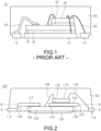
- FIG. 1 is a cross-sectional side view of a conventional power die package 10, which is assembled using a lead frame having a flag 12 and leads 14 that surround the flag 12.
- a power die 16 is attached to a top surface of the flag 12 with a lead free die attach adhesive 18 and a control die 20 is attached to a top surface of the power die 18 with an adhesive film 22.
- the power die 16 is electrically connected to a first set of the leads 14 with thick aluminum bond wires 24 ( e.g., 15mil diameter), while the control die 20 is electrically connected to a second set of the leads 14 with thin copper bond wires 26 ( e.g., 1.5mil diameter).
- the entire assembly is covered with an encapsulant 28.
- the encapsulant 28 is provided to protect the dies 16 and 20 and the wire bonds from being damaged.
- the power die 16 generates heat that must be dissipated, so the flag 12 is formed of a relatively thick sheet of copper and the die attach adhesive must have good thermal properties, which factors increase the overall cost of the package 10. It would be advantageous to reduce the assembly cost of such power die packages.
- US20130181332 discloses a leadframe for a device which provides not only structural support and connectivity to the I/O pins to the external world, but also for housing and/or mounting devices above and below the leadframe.
- US20090189266 discloses a buck converter package with stacked dice and a process for forming a buck converter. The package includes a die attach pad with a low side die mounted on one surface and a high side die mounted on the opposing surface.
- US9214416 B1 discloses a new Power DFN and Power QFN package architecture that accommodates Bump-chip die and other components in cavities on the bottom-side of the matrix leadframe.
- US20110096509 discloses a module including a first functional device and a second functional device.
- US20020149103 discloses a multi-chip semiconductor package in which a first chip and a second chip are mounted on opposing surfaces of a lead frame in a staggered manner.
- US 20110049690 discloses a direct contact leadless package suitable for packaging high current semiconductor devices. The package comprising a first contact lead frame portion, a paddle portion, and an extended contact lead frame portion held together by a mold compound.
- US7335532 B2 discloses a multichip module package that uses bond wire with plastic resin on one side of a lead frame to package an integrated circuit and flip chip techniques to attach one or more mosfets to the other side of the lead frame.
- a power die package comprising: a lead frame having a flag having an upper surface for receiving a control die and a lower surface for receiving a power die, a plurality of power leads adjacent to and spaced from a first lateral side of the flag and a plurality of signal leads adjacent to and spaced from at least one other lateral side of the flag, wherein the power leads have proximal ends nearer to the flag and distal ends spaced further from the flag; a control die having a back side attached to the upper surface of the flag and an active side opposite said back side that includes a plurality of control die electrodes, wherein a first set of the control die electrodes are electrically connected to the plurality of signal leads; and a power die having a first side attached to the lower surface of the flag, wherein the power die has a plurality of power die electrodes including a first set of power die electrodes that are electrically connected to the plurality of power leads.
- the first set of control die electrodes is electrically connected to the plurality of signal leads with first bond wires.
- the power die package further comprises a second set of the control die electrodes, different from the first set of control die electrodes, that is electrically connected to a second set of the power die electrodes, different from the first set of power die electrodes, with second bond wires.
- the power die has a larger footprint than the flag such that a portion of the power die including the first set of power die electrodes overhangs the flag.
- the first set of power die electrodes is in direct contact with the plurality of power die leads.
- the signal leads and the distal ends of the power die leads may lie in a first plane and proximal ends of the power die leads and the flag may lie in a second plane, wherein the second plane is parallel to and spaced from the first plane, such that the proximal ends of the power die leads rest on top of and are in electrical contact with the first set of power die electrodes.
- an active surface of the power die may be attached to the lower surface of the flag with a conductive epoxy and the proximal ends of the power die leads are attached to the first set of power die electrodes also with conductive epoxy.
- control die may have a smaller footprint than the flag such that the control die is disposed within the footprint of the flag.
- control die may be attached to the flag with a die attach adhesive tape.
- the flag may be rectangular, and the power leads may be adjacent to the first lateral side of the flag and the signal leads may be spaced around the remaining three other sides of the flag.
- the power die package may further comprise a mold compound that encases the flag, the proximal ends of the power leads, the signal leads, the control die, the power die, and the electrical connections between the power leads and the power die electrodes and the signal leads and the first set of control die electrodes, wherein a bottom surface of the power die is exposed.
- the power die package may further comprise a layer of solder formed over the exposed bottom surface of the power die.
- the package may comprise a quad flat no-leads (QFN) package.
- QFN quad flat no-leads
- the first set of control die electrodes are electrically connected to the plurality of signal leads with first bond wires; a second set of the control die electrodes, different from the first set of control die electrodes, are electrically connected to a second set of the power die electrodes, different from the first set of power die electrodes, with second bond wires;
- the power die has a larger footprint than the flag such that a portion of the power die including the first set of power die electrodes overhangs the flag;
- the first set of power die electrodes is in direct contact with the plurality of power die leads;
- the signal leads and the distal ends of the power die leads may lie in a first plane and proximal ends of the power die leads and the flag may lie in a second plane, wherein the second plane is parallel to and spaced from the first plane, such that the proximal ends of the power die leads rest on top of and are in electrical contact with the first set of power die electrodes;
- an active surface of the power die may be attached to the lower surface of the flag with a
- a method of assembling a power die package comprising: providing a lead frame including a flag having an upper surface for receiving a control die and a lower surface for receiving a power die, a plurality of power leads adjacent to and spaced from a first lateral side of the flag and a plurality of signal leads adjacent to and spaced from at least one other lateral side of the flag, wherein the power leads have proximal ends nearer to the flag and distal ends spaced further from the flag; attaching an active side of a power die to the lower surface of the flag, wherein the power die has a larger footprint than the flag such that a portion of the power die overhangs the flag, and wherein the portion of the power die that overhangs the flag has a plurality of power die electrodes including a first set of power die electrodes that are in contact with and electrical communication with the proximal ends of the power leads; attaching a back side of a control die to the upper surface of the flag, wherein an active side of
- the method may further comprise encasing the flag, the proximal ends of the power leads, the signal leads, the control die, the power die, the electrical connections between the power leads and the first set of power die electrodes, and the first bond wires with a mold compound, wherein a bottom surface of the power die is exposed.
- the method may further comprise forming a layer of solder over the exposed bottom surface of the power die.
- the method may further comprise performing a trim and form step on exposed portions of the power leads and the signal leads to form a Quad Flat No-leads (QFN) package.
- QFN Quad Flat No-leads
- the signal leads and the distal ends of the power die leads may lie in a first plane and proximal ends of the power die leads and the flag may lie in a second plane, wherein the second plane is parallel to and spaced from the first plane, such that the proximal ends of the power die leads rest on top of and are in electrical contact with the first set of power die electrodes.
- the power die may be attached to the flag with a conductive epoxy and the control die may be attached to the flag with a non-conductive die attach adhesive.
- the present invention provides a power die package comprising a lead frame, a control die and a power die.
- the lead frame includes a flag having a top or upper surface for receiving the control die and a bottom or lower surface for receiving the power die.
- the lead frame also has a plurality of power leads adjacent to and spaced from a first lateral side of the flag and a plurality of signal leads adjacent to and spaced from at least one other lateral side of the flag.
- the power leads have proximal ends near to the flag and distal ends spaced further from the flag.
- the control die has a back side attached to the upper surface of the flag and an active side opposite to the back side that includes a plurality of control die electrodes.
- a first set of the control die electrodes are electrically connected to the plurality of signal leads with first bond wires.
- the power die has a first side attached to the lower surface of the flag.
- the power die has a plurality of power die electrodes including a first set of power die electrodes that are electrically connected to the plurality of power leads.
- a second set of the control die electrodes are connected to a second set of the power die electrodes with second bond wires, and the entire assembly is covered with a mold compound.
- the present invention also provides a method of assembling a power die package, including providing a lead frame having a flag with a top or upper surface for receiving a control die and a bottom or lower surface for receiving a power die.
- the lead frame also has a plurality of power leads adjacent to and spaced from a first lateral side of the flag and a plurality of signal leads adjacent to and spaced from at least one other lateral side of the flag.
- the power leads have proximal ends near to the flag and distal ends spaced further from the flag.
- An active side of a power die is attached to the lower surface of the flag.
- the power die has a larger footprint than the flag such that a portion of the power die overhangs the flag, and the portion of the power die that overhangs the flag has a plurality of power die electrodes including a first set of power die electrodes that are in contact with and electrical communication with the proximal ends of the power leads.
- a back side of a control die is attached to the upper surface of the flag.
- An active side of the control die, opposite the back side of the flag, includes a plurality of control die electrodes.
- a first set of the control die electrodes is electrically connected to the plurality of signal leads with first bond wires, and then the flag, the proximal ends of the power leads, the signal leads, the control die, the power die, the electrical connections between the power leads and the first set of power die electrodes, and the first bond wires are encased with a mold compound, where a bottom surface of the power die is exposed.
- the present invention provides a lower cost power die package than presently available packages because the lead frame is less expensive and thick Aluminum bond wires are not needed.
- the cost of attaching the power die to the flag is less because either a lower cost die attach material may be used or less of a more expensive die attach material is required because the entire bottom surface of the power die is not attached to the flag.
- the package of the present invention also may have better thermal properties than the conventional power die package because the bottom side of the power die is exposed.
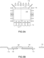
- the power die package 100 includes a lead frame having a flag 102 having a top or upper surface 104 for receiving a control die and a bottom or lower surface 106 for receiving a power die.
- the lead frame also has a plurality of power leads 108 adjacent to and spaced from a first lateral side of the flag 102 and a plurality of signal leads 110 adjacent to and spaced from at least one other lateral side of the flag 102.
- the power leads 108 have proximal ends 112 near to the flag 102 and distal ends 114 spaced further from the flag 102.
- a control die 116 has a back side that is attached to the upper surface 104 of the flag 102 and an active side, which is opposite to its back side, that includes a plurality of control die electrodes.
- a first set of the control die electrodes are electrically connected to the plurality of signal leads 110.
- the first plurality of control die electrodes are connected to the signal leads 110 with first bond wires 118.
- the first bond wires 118 may comprise copper, gold or other conductive metal wires, as is known in the art and connected to the die electrodes and the lead frame leads 110 using commercially available wire bonding equipment.
- a power die 120 has a first or active side attached to the lower surface 106 of the flag 102.
- the power die 120 has a plurality of power die electrodes on its active side, including a first set of power die electrodes, that are electrically connected to the plurality of power leads 108. More particularly, in accordance with the presently preferred embodiment of the invention, the proximal ends 112 of the power leads 108 are in direct contact with the first set of power die electrodes.
- the control die 116 is attached to the upper surface 104 of the die flag 102 with a die attach material 122, such as a die attach epoxy or a die attach adhesive tape, both of which are known in the art and commercially available.
- the power die 120 is attached to the lower surface 106 of the die flag 102 with a conductive epoxy 124.
- the proximal ends 112 of the power leads 108 are connected to the first set of power die electrodes also with a conductive epoxy 126.
- the conductive epoxies 124 and 126 preferably comprise the same material.
- the die attach material 122 can be conductive or non-conductive, while the epoxies 124 and 126 are conductive epoxies. Suitable conductive and non-conductive epoxies are known by those of skill in the art and readily commercially available.
- the signal leads 110 and the distal ends 114 of the power die leads 108 lie in a first plane A-A and the proximal ends 112 of the power die leads 108 and the flag 102 lie in a second plane B-B.
- the second plane B-B is parallel to and spaced from the first plane A-A, such that the proximal ends 112 of the power die leads 108 rest on top of and are in electrical contact with the first set of power die electrodes.
- the power die 120 has a larger footprint than the flag 102 such that a portion of the power die 120 including the first set of power die electrodes overhangs the flag 102. Then the proximal ends 112 of the power leads 108 can contact the first set of power die electrodes yet still be spaced from the flag 102. Within the space between the flag 102 and the proximal ends 112 of the power leads 108, a surface of the power die 120 is exposed, and there is a second set of power die electrodes located in this exposed space.
- the control die 116 which is attached to the top surface 104 of the flag 102, preferably has a smaller footprint than the flag 102, as shown in FIG. 2 .
- FIG. 2 is not necessarily drawn to scale, it shows that in the preferred embodiment, the control die 116 is smaller than the power die 120 and the flag 104.
- the control die 116 also has a second set of electrodes that are electrically connected to the second set of power die electrodes with second bond wires 128.
- a mold compound 130 encases the flag 102, the proximal ends 112 of the power leads 108, the signal leads 110, the control die 116, the power die 120, and the first and second bond wires 118 and 128.
- the mold compound 130 protects the dies 116 and 120, the bond wires 118 and 128, and the wire bonds from being damaged.
- the mold compound 130 also defines a package body. Exposed are distal ends 114 of the power leads 108, side and bottom surfaces of the signal leads 110, and the bottom side of the power die 120. The exposed portions of the leads 108 and 110 allow for external electrical connection to the device 100.
- a metal coating 132 such as a layer of solder is formed over the exposed bottom surface of the power die 120.
- the purpose of the metal coating 132 is to prevent the bottom of power die from mechanical damage during device level electrical testing and handling, prior to surface mount.
- the lead frame may be formed of copper or other conductive metals, as is known in the art, and may be supplied in either strip or array form.
- the lead frame or just selected portions of the lead frame, like outer lead areas of the leads, may be coated or plated with another metal or alloy to inhibit corrosion when the lead frame is exposed to the ambient environment.
- the lead frame may be formed from a sheet of copper or copper foil by cutting, stamping, and/or etching.
- the die receiving area 102 comprises a die pad, that is, a solid piece of copper upon which the dies 116 and 120 are mounted.
- the die pad may be made relatively thick so that it can act as a heat sink, absorbing heat generated by the dies 116 and 120.
- the control die 116 may comprise a digital circuit that receives signals from and provides signals to other integrated circuit chips, while the power die 120 may comprise an analog circuit, such as power MOSFET.
- the device 100 may comprise an integrated circuit that can be used, for example, to control automotive headlamps, such as an NXP eSwitch (extreme Switch) available from NXP B.V. of the Netherlands, which includes features such as a 16-bit SPI with daisy chain capability, a PWM module with external or internal clock, smart over-current shutdown, over-temperature protections, auto-retry on most protections, a fail-safe mode, open load detection for bulbs or LEDs, short to battery detection, and analog current and temperature feedback.
- NXP eSwitch Extreme Switch
- FIG. 3 is a flow chart 150 of a method of assembling the package 10 shown in FIG. 2 and FIGS. 4-8 illustrate the package 10 in various stages of the assembly process.
- a preliminary step 152 wafer dicing is performed to provide a plurality of power dies and a plurality of control dies.
- the power dies and control dies are fabricated on separate wafers, but the dicing step may be performed on both of the wafers at the same assembly site.
- a lead frame like the lead frame shown 170 shown in FIGS. 4A and 4B is shown. More particularly, FIGS. 4A and 4B show a portion of a lead frame 170 in accordance with an embodiment of the present invention.
- the lead frame 170 is part of an array of lead frames so that multiple packages may be assembled simultaneously.
- the lead frame 170 includes a flag 172, a plurality of power leads 174, and a plurality of signal leads 176.
- the flag 172 has an upper surface 178 for receiving a control die and a lower surface 180 for receiving a power die.
- the power leads 174 are located adjacent to and spaced from a first lateral side 182 of the flag 172, while the signal leads 176 are adjacent to and spaced from at least one other lateral side of the flag 172. In the embodiment shown, the signal leads 176 are disposed around the remaining three lateral sides of the flag 172.
- the power leads 174 have proximal ends 184 near to the flag 172 and distal ends 186 spaced further from the flag 172. As can be seen in FIG.
- the flag 172 and the proximal ends 184 of the power leads 174 lie in a first plane and the signal leads 176 and the distal ends 186 of the power leads 174 lie in a second plane that is spaced from and parallel to the first plane.
- the lead frame 170 may be formed at the assembly site or formed at a by a lead frame supplier and as previously discussed, the lead frame may be plated with a metal, metals, or an alloy to prevent corrosion.
- a power die is attached to the lead frame.
- the lead frame 170 is turned over so that the bottom side 180 faces up, as shown in FIGS. 4A and 4B and a conductive epoxy 188 is disposed on the bottom side 180 of the flag 172 and the proximal ends 184 of the power leads 174.
- the conductive epoxy 188 may be dispensed onto the flag 172 and the power leads 174 in an X-pattern or as a blob or smear (no particular shape).
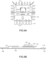
- FIGS. 5A and 5B show an active side of power die 190 attached to the lower or bottom surface of the flag 172.
- the power die 190 has a larger footprint than the flag 172 such that a portion of the power die 190 overhangs the flag 172, and the portion of the power die 190 that overhangs the flag 172 has a plurality of power die electrodes including a first set of power die electrodes that are in contact with and electrical communication with the proximal ends 184 of the power leads 174.
- the power die 190 spans the space between the flag 172 and the power leads 174, and rests on both of the flag 172 and the power leads 174. Referring to FIG.
- the right-hand side of the drawing shows the lateral side of the flag 172 and the lateral side of the power die 190 are not aligned, it is not a requirement that the flag 172 and the power die are not aligned. For example, if the flag 172 was less wide so that it's lateral side was aligned with the lateral side of the power die 190, then the lead frame would use less metal.
- step 156 after attaching the power die 190, a tape 192 is placed over the distal ends 186 of the power leads 174, the power die 190, and the signal leads 176, as shown in FIG. 6B .
- the assembly is then turned over and step 158, attaching a control die 194 is performed.
- the control die 194 is attached to upper surface 178 of the flag 172 with a die attach film or die attach epoxy 196.
- the control die 194 is attached with its active side up so that a plurality of first electrodes 198 and a plurality of second electrodes 200 are accessible.
- the power die 190 also has a plurality of second electrodes 202 that are located on the power die 190 and visible in the gap between the flag 172 and the power leads 174.
- first electrical connections are made between the first set of control die electrodes 198 and the signal leads 176
- second electrical connections are made between the second set of control die electrodes 200 and the power die 190. More particularly, as shown in FIGS. 7A and 7B , the first set of the control die electrodes 198 are electrically connected with the plurality of signal leads 176 with first bond wires 204 and the second set of control die electrodes 200 are electrically connected with the second set of power die electrodes 202 with second bond wires 206.
- the first and second bond wires 204 and 206 may comprise the same wire type, e.g., 1.5mil copper wire.
- a mold compound 208 is formed over the dies 190 and 194, the first and second bond wires 204 and 206, and portions of the power leads 174 and the signal leads 176, as shown in FIG. 8 .
- the mold compound 208 may be formed over the assembly using a "molded array packaging" or MAP process, which is known in the art. After molding, a bottom surface of the power die 190 is exposed, as are portions of the signal leads 176 and the distal ends 186 of the power leads 174. Also after molding, the tape 192 is removed.
- FIGS. 9A and 9B are top and bottom plan views of a power device 212 assembled in accordance with the above-described method.
- FIG. 9A portions of the power leads 174, signal leads 176 and the mold compound 208 are visible, while in the bottom view, FIG. 9B , more of the power leads 174 and signal leads 176 are visible.
- the bottom surface of the power die 190 also is exposed, as noted above with reference to FIG. 8 .
- the bottom exposed surface of the power die 190 is coated with a conductive material, such as gold or solder.
- the bottom surface of the power die 190 is coated with gold 210. Trim and form operations may be performed, as needed, to complete the formation of a Quad Flag No-leads (QFN) package.
- QFN Quad Flag No-leads
- the present invention comprises a lead frame for a PQFN type package.
- the PQFN has a lower parts and assembly cost that present power devices because the lead frame may be formed using a punching process, which costs less than processes that require etching. Moreover, the flag and leads may have the same thickness, thus cost is not increased by having a more complicated lead frame structure.
- the power die is directly connected to the power leads, so there is no need for a separate wire bonding process that uses expensive thick aluminum wires. Both dies also fit onto opposing sides of the lead frame flag.
- a power die package includes a lead frame having a flag with power leads on one lateral side and signal leads on one or more other lateral sides.
- a power die is attached to a bottom surface of the flag and electrically connected to the power leads with a conductive epoxy.
- a control die is attached to a top surface of the flag and electrically connected to the signal leads with bond wires.
- a mold compound is provided that encapsulates the dies, the bond wires, and proximal parts of the leads, while distal ends of the leads are exposed, forming a PQFN package.
Landscapes
- Lead Frames For Integrated Circuits (AREA)
- Engineering & Computer Science (AREA)
- Manufacturing & Machinery (AREA)
Claims (12)
- Boîtier de puce de puissance (100), comprenant :une grille de connexion (170) ayant un drapeau (102, 172) ayant une surface supérieure (104) destinée à recevoir une puce de commande (116, 194) et une surface inférieure (106, 180) destinée à recevoir une puce de puissance (120, 190), une pluralité de broches d'alimentation (108, 174) adjacentes à et espacées d'un premier côté latéral (182) du drapeau et une pluralité de broches de signaux (110, 176) adjacentes à et espacées d'au moins un autre côté latéral du drapeau (102, 172), les broches d'alimentation ayant des extrémités proximales (112) plus proches du drapeau et des extrémités distales (114) plus éloignées du drapeau ;la puce de commande (116, 194) ayant un côté arrière fixé à la surface supérieure du drapeau et un côté actif à l'opposé dudit côté arrière qui comporte une pluralité d'électrodes de puce de commande, un premier ensemble des électrodes de puce de commande (198) étant connectées électriquement à la pluralité de broches de signaux ; etla puce de puissance (120, 190) ayant un premier côté fixé à la surface inférieure du drapeau, la puce de puissance ayant une pluralité d'électrodes de puce de puissance, y compris un premier ensemble d'électrodes de puce de puissance qui sont connectées électriquement à la pluralité de broches d'alimentation, dans lequelle premier ensemble d'électrodes de puce de commande (198) sont connectées électriquement à la pluralité de broches de signaux (110, 176) avec des premiers films de connexion (118, 204), etle boîtier de puce de puissance comprenant en outre un deuxième ensemble des électrodes de puce de commande (200), différent du premier ensemble d'électrodes de puce de commande (198), qui est connecté électriquement à un deuxième ensemble des électrodes de puce de puissance (202), différent du premier ensemble d'électrodes de puce de puissance, avec des deuxièmes fils de connexion (128, 206), dans lequella puce de puissance (120, 190) a une plus grande empreinte que le drapeau (102, 172) de telle sorte qu'une partie de la puce de puissance comportant le premier ensemble d'électrodes de puce de puissance surplombe le drapeau, etdans lequel le premier ensemble d'électrodes de puce de puissance sont en contact direct avec la pluralité de broches d'alimentation (108, 174).
- Boîtier de puce de puissance (100) selon la revendication 1, dans lequel les broches de signaux (110, 176) et les extrémités distales (114) des broches d'alimentation (108, 174) se situent dans un premier plan et des extrémités proximales (112) des broches d'alimentation et le drapeau (102, 172) se situent dans un deuxième plan, le deuxième plan étant parallèle au et espacé du premier plan, de telle sorte que les extrémités proximales des broches d'alimentation reposent sur le dessus du et sont en contact électrique avec le premier ensemble d'électrodes de puce de puissance.
- Boîtier de puce de puissance (100) selon la revendication 2, dans lequel une surface active de la puce de puissance (120, 190) est fixée à la surface inférieure du drapeau (102, 172) avec une résine époxy conductrice (124) et les extrémités proximales (112) des broches d'alimentation (108, 174) sont fixées au premier ensemble d'électrodes de puce de puissance également avec de la résine époxy conductrice (126).
- Boîtier de puce de puissance (100) selon l'une quelconque des revendications 1 à 3, dans lequel la puce de commande (116, 194) a une plus petite empreinte que le drapeau (102, 172) de telle sorte que la puce de commande est disposée à l'intérieur de l'empreinte du drapeau.
- Boîtier de puce de puissance (100) selon la revendication 4, dans lequel la puce de commande (116, 194) est fixée au drapeau (102, 172) avec un ruban adhésif de fixation de puce (122).
- Boîtier de puce de puissance (100) selon une quelconque revendication précédente, dans lequel le drapeau (102, 172) est rectangulaire, et les broches d'alimentation (108, 174) sont adjacentes au premier côté latéral (182) du drapeau et les broches de signaux (110, 176) sont espacées autour des trois autres côtés restants du drapeau.
- Boîtier de puce de puissance (100) selon une quelconque revendication précédente, comprenant en outre un composé de moulage (130) qui encapsule le drapeau (102, 172), les extrémités proximales (112) des broches d'alimentation (108, 174), les broches de signaux (110, 176), la puce de commande (116, 194), la puce de puissance (120, 190), et les connexions électriques entre les broches d'alimentation et les électrodes de puce de puissance et les broches de signaux et le premier ensemble d'électrodes de puce de commande (198), dans lequel une surface inférieure de la puce de puissance est exposée.
- Boîtier de puce de puissance (100) selon la revendication 7, comprenant en outre une couche de soudure (132) formée par-dessus la surface inférieure exposée de la puce de puissance (120, 190).
- Boîtier de puce de puissance (100) selon la revendication 7 ou 8, le boîtier comprenant un boîtier plat sans broches (QFN).
- Boîtier de puce de puissance (100) selon l'une quelconque des revendications 7 à 9, dans lequel :les broches de signaux (110, 176) et les extrémités distales (114) des broches d'alimentation se situent dans un premier plan (A-A) et des extrémités proximales (112) des broches d'alimentation et le drapeau se situent dans un deuxième plan (B-B), le deuxième plan étant parallèle au et espacé du premier plan, de telle sorte que les extrémités proximales des broches d'alimentation reposent sur le dessus du et sont en contact électrique avec le premier ensemble d'électrodes de puce de puissance ;une surface active de la puce de puissance est fixée à la surface inférieure du drapeau avec une résine époxy conductrice (124) et les extrémités proximales des broches d'alimentation sont fixées au premier ensemble d'électrodes de puce de puissance également avec de la résine époxy conductrice (126) ;la puce de commande (116, 194) a une plus petite empreinte que le drapeau (102, 172) de telle sorte que la puce de commande est disposée à l'intérieur de l'empreinte du drapeau ; etla puce de commande est fixée au drapeau avec un ruban adhésif de fixation de puce (122).
- Procédé (150) d'assemblage d'un boîtier de puce de puissance, comprenant :l'obtention (152) d'une grille de connexion comportant un drapeau ayant une surface supérieure destinée à recevoir une puce de commande et une surface inférieure destinée à recevoir une puce de puissance, une pluralité de broches d'alimentation adjacentes à et espacées d'un premier côté latéral du drapeau et une pluralité de broches de signaux adjacentes à et espacées d'au moins un autre côté latéral du drapeau, les broches d'alimentation ayant des extrémités proximales plus proches du drapeau et des extrémités distales plus éloignées du drapeau ;la fixation (154) d'un côté actif de la puce de puissance à la surface inférieure du drapeau, la puce de puissance ayant une plus grande empreinte que le drapeau de telle sorte qu'une partie de la puce de puissance surplombe le drapeau, et la partie de la puce de puissance qui surplombe le drapeau ayant une pluralité d'électrodes de puce de puissance, y compris un premier ensemble d'électrodes de puce de puissance qui sont en contact direct et en communication électrique avec les extrémités proximales des broches d'alimentation ;la fixation (158) d'un côté arrière de la puce de commande à la surface supérieure du drapeau, un côté actif de la puce de commande à l'opposé dudit côté arrière du drapeau comportant une pluralité d'électrodes de puce de commande ;la connexion électrique (160) d'un premier ensemble des électrodes de puce de commande à la pluralité de broches de signaux avec des premiers fils de connexion ;la connexion électrique d'un deuxième ensemble des électrodes de puce de puissance, différent du premier ensemble d'électrodes de puce de puissance, avec des deuxièmes fils de connexion.
- Procédé selon la revendication 11, comprenant en outre :
l'encapsulation (162) du drapeau, des extrémités proximales des broches d'alimentation, des broches de signaux, de la puce de commande, de la puce de puissance, des connexions électriques entre les broches d'alimentation et le premier ensemble d'électrodes de puce de puissance et des premiers fils de connexion avec un composé de moulage, dans lequel une surface inférieure de la puce de puissance est exposée.
Applications Claiming Priority (1)
| Application Number | Priority Date | Filing Date | Title |
|---|---|---|---|
| CN201910566612.XA CN112151513A (zh) | 2019-06-27 | 2019-06-27 | 功率管芯封装 |
Publications (2)
| Publication Number | Publication Date |
|---|---|
| EP3761360A1 EP3761360A1 (fr) | 2021-01-06 |
| EP3761360B1 true EP3761360B1 (fr) | 2024-09-25 |
Family
ID=71108358
Family Applications (1)
| Application Number | Title | Priority Date | Filing Date |
|---|---|---|---|
| EP20180353.3A Active EP3761360B1 (fr) | 2019-06-27 | 2020-06-16 | Boîtier de puces de puissance |
Country Status (3)
| Country | Link |
|---|---|
| US (1) | US11515238B2 (fr) |
| EP (1) | EP3761360B1 (fr) |
| CN (1) | CN112151513A (fr) |
Families Citing this family (2)
| Publication number | Priority date | Publication date | Assignee | Title |
|---|---|---|---|---|
| CN115602673A (zh) * | 2021-06-28 | 2023-01-13 | 杰群电子科技(东莞)有限公司(Cn) | 一种多芯片混合封装结构 |
| US11621215B1 (en) * | 2021-11-30 | 2023-04-04 | Texas Instruments Incorporated | Semiconductor device package with isolated semiconductor die and electric field curtailment |
Citations (2)
| Publication number | Priority date | Publication date | Assignee | Title |
|---|---|---|---|---|
| US7335532B2 (en) * | 2004-03-18 | 2008-02-26 | Fairchild Semiconductor Corporation | Method of assembly for multi-flip chip on lead frame on overmolded IC package |
| US20110049690A1 (en) * | 2009-08-28 | 2011-03-03 | International Rectifier Corporation | Direct contract leadless package for high current devices |
Family Cites Families (20)
| Publication number | Priority date | Publication date | Assignee | Title |
|---|---|---|---|---|
| US5894108A (en) | 1997-02-11 | 1999-04-13 | National Semiconductor Corporation | Plastic package with exposed die |
| US6137165A (en) | 1999-06-25 | 2000-10-24 | International Rectifier Corp. | Hybrid package including a power MOSFET die and a control and protection circuit die with a smaller sense MOSFET |
| US6376914B2 (en) | 1999-12-09 | 2002-04-23 | Atmel Corporation | Dual-die integrated circuit package |
| US6717260B2 (en) | 2001-01-22 | 2004-04-06 | International Rectifier Corporation | Clip-type lead frame for source mounted die |
| TW488045B (en) * | 2001-04-12 | 2002-05-21 | Siliconware Precision Industries Co Ltd | Semiconductor package with dislocated multi-chips |
| US7061080B2 (en) | 2001-06-11 | 2006-06-13 | Fairchild Korea Semiconductor Ltd. | Power module package having improved heat dissipating capability |
| JP3540793B2 (ja) * | 2001-12-05 | 2004-07-07 | 松下電器産業株式会社 | 樹脂封止型半導体装置及びその製造方法 |
| JP2009043820A (ja) * | 2007-08-07 | 2009-02-26 | Rohm Co Ltd | 高効率モジュール |
| US8063472B2 (en) * | 2008-01-28 | 2011-11-22 | Fairchild Semiconductor Corporation | Semiconductor package with stacked dice for a buck converter |
| US9449957B2 (en) | 2010-12-13 | 2016-09-20 | Infineon Technologies Americas Corp. | Control and driver circuits on a power quad flat no-lead (PQFN) leadframe |
| US20120228696A1 (en) | 2011-03-07 | 2012-09-13 | Texas Instruments Incorporated | Stacked die power converter |
| CN102263080B (zh) * | 2011-07-29 | 2015-06-17 | 天水华天科技股份有限公司 | 带双凸点的四边扁平无引脚三ic芯片封装件及其生产方法 |
| US8951847B2 (en) * | 2012-01-18 | 2015-02-10 | Intersil Americas LLC | Package leadframe for dual side assembly |
| US8546955B1 (en) | 2012-08-16 | 2013-10-01 | Xilinx, Inc. | Multi-die stack package |
| US9966330B2 (en) | 2013-03-14 | 2018-05-08 | Vishay-Siliconix | Stack die package |
| US9214416B1 (en) * | 2013-06-22 | 2015-12-15 | Courtney Furnival | High speed, low loss and high density power semiconductor packages (μMaxPak) with molded surface mount high speed device(s) and multi-chip architectures |
| CN104900623B (zh) | 2014-03-06 | 2018-11-30 | 恩智浦美国有限公司 | 露出管芯的功率半导体装置 |
| US9263299B2 (en) | 2014-07-02 | 2016-02-16 | Nxp B.V. | Exposed die clip bond power package |
| EP3018710B1 (fr) | 2014-11-10 | 2020-08-05 | Nxp B.V. | Assemblage des puces semi-conductrices |
| US9806067B2 (en) | 2015-07-20 | 2017-10-31 | Globalfoundries Inc. | Die-die stacking |
-
2019
- 2019-06-27 CN CN201910566612.XA patent/CN112151513A/zh active Pending
-
2020
- 2020-06-16 EP EP20180353.3A patent/EP3761360B1/fr active Active
- 2020-06-17 US US16/903,496 patent/US11515238B2/en active Active
Patent Citations (2)
| Publication number | Priority date | Publication date | Assignee | Title |
|---|---|---|---|---|
| US7335532B2 (en) * | 2004-03-18 | 2008-02-26 | Fairchild Semiconductor Corporation | Method of assembly for multi-flip chip on lead frame on overmolded IC package |
| US20110049690A1 (en) * | 2009-08-28 | 2011-03-03 | International Rectifier Corporation | Direct contract leadless package for high current devices |
Also Published As
| Publication number | Publication date |
|---|---|
| US11515238B2 (en) | 2022-11-29 |
| CN112151513A (zh) | 2020-12-29 |
| EP3761360A1 (fr) | 2021-01-06 |
| US20200411423A1 (en) | 2020-12-31 |
Similar Documents
| Publication | Publication Date | Title |
|---|---|---|
| US8836101B2 (en) | Multi-chip semiconductor packages and assembly thereof | |
| US6198163B1 (en) | Thin leadframe-type semiconductor package having heat sink with recess and exposed surface | |
| TWI453838B (zh) | 具有散熱器之無引線封裝 | |
| US8575742B1 (en) | Semiconductor device with increased I/O leadframe including power bars | |
| US7847392B1 (en) | Semiconductor device including leadframe with increased I/O | |
| US20080029860A1 (en) | Semiconductor device with internal heat sink | |
| US8089145B1 (en) | Semiconductor device including increased capacity leadframe | |
| US20100193922A1 (en) | Semiconductor chip package | |
| US10840172B2 (en) | Leadframe, semiconductor package including a leadframe and method for forming a semiconductor package | |
| KR20050109502A (ko) | 내장형 수동 소자를 갖는 리드 프레임 | |
| US10090228B1 (en) | Semiconductor device with leadframe configured to facilitate reduced burr formation | |
| US7566967B2 (en) | Semiconductor package structure for vertical mount and method | |
| US9076891B2 (en) | Integrated circuit (“IC”) assembly includes an IC die with a top metallization layer and a conductive epoxy layer applied to the top metallization layer | |
| EP3761360B1 (fr) | Boîtier de puces de puissance | |
| KR20050079145A (ko) | 리드 프레임, 이를 이용한 반도체 칩 패키지 및 그의 제조방법 | |
| US20100295160A1 (en) | Quad flat package structure having exposed heat sink, electronic assembly and manufacturing methods thereof | |
| US20230136784A1 (en) | Semiconductor device package with thermal pad | |
| US20130020689A1 (en) | Semiconductor device and method of packaging same | |
| US12125780B2 (en) | Extendable inner lead for leaded package | |
| US20060145312A1 (en) | Dual flat non-leaded semiconductor package | |
| US11171077B2 (en) | Semiconductor device with lead frame that accommodates various die sizes | |
| US8574961B2 (en) | Method of marking a low profile packaged semiconductor device | |
| EP4481808A1 (fr) | Dispositif semi-conducteur à double grille de connexion et procédé associé | |
| US7951651B2 (en) | Dual flat non-leaded semiconductor package | |
| KR20020065733A (ko) | 반도체 패키지 및 그 제조방법 |
Legal Events
| Date | Code | Title | Description |
|---|---|---|---|
| PUAI | Public reference made under article 153(3) epc to a published international application that has entered the european phase |
Free format text: ORIGINAL CODE: 0009012 |
|
| STAA | Information on the status of an ep patent application or granted ep patent |
Free format text: STATUS: THE APPLICATION HAS BEEN PUBLISHED |
|
| AK | Designated contracting states |
Kind code of ref document: A1 Designated state(s): AL AT BE BG CH CY CZ DE DK EE ES FI FR GB GR HR HU IE IS IT LI LT LU LV MC MK MT NL NO PL PT RO RS SE SI SK SM TR |
|
| AX | Request for extension of the european patent |
Extension state: BA ME |
|
| STAA | Information on the status of an ep patent application or granted ep patent |
Free format text: STATUS: REQUEST FOR EXAMINATION WAS MADE |
|
| 17P | Request for examination filed |
Effective date: 20210706 |
|
| RBV | Designated contracting states (corrected) |
Designated state(s): AL AT BE BG CH CY CZ DE DK EE ES FI FR GB GR HR HU IE IS IT LI LT LU LV MC MK MT NL NO PL PT RO RS SE SI SK SM TR |
|
| STAA | Information on the status of an ep patent application or granted ep patent |
Free format text: STATUS: EXAMINATION IS IN PROGRESS |
|
| 17Q | First examination report despatched |
Effective date: 20220405 |
|
| GRAP | Despatch of communication of intention to grant a patent |
Free format text: ORIGINAL CODE: EPIDOSNIGR1 |
|
| STAA | Information on the status of an ep patent application or granted ep patent |
Free format text: STATUS: GRANT OF PATENT IS INTENDED |
|
| INTG | Intention to grant announced |
Effective date: 20240628 |
|
| GRAS | Grant fee paid |
Free format text: ORIGINAL CODE: EPIDOSNIGR3 |
|
| GRAA | (expected) grant |
Free format text: ORIGINAL CODE: 0009210 |
|
| STAA | Information on the status of an ep patent application or granted ep patent |
Free format text: STATUS: THE PATENT HAS BEEN GRANTED |
|
| AK | Designated contracting states |
Kind code of ref document: B1 Designated state(s): AL AT BE BG CH CY CZ DE DK EE ES FI FR GB GR HR HU IE IS IT LI LT LU LV MC MK MT NL NO PL PT RO RS SE SI SK SM TR |
|
| REG | Reference to a national code |
Ref country code: GB Ref legal event code: FG4D |
|
| REG | Reference to a national code |
Ref country code: CH Ref legal event code: EP |
|
| REG | Reference to a national code |
Ref country code: DE Ref legal event code: R096 Ref document number: 602020038203 Country of ref document: DE |
|
| REG | Reference to a national code |
Ref country code: IE Ref legal event code: FG4D |
|
| REG | Reference to a national code |
Ref country code: LT Ref legal event code: MG9D |
|
| PG25 | Lapsed in a contracting state [announced via postgrant information from national office to epo] |
Ref country code: NO Free format text: LAPSE BECAUSE OF FAILURE TO SUBMIT A TRANSLATION OF THE DESCRIPTION OR TO PAY THE FEE WITHIN THE PRESCRIBED TIME-LIMIT Effective date: 20241225 |
|
| PG25 | Lapsed in a contracting state [announced via postgrant information from national office to epo] |
Ref country code: GR Free format text: LAPSE BECAUSE OF FAILURE TO SUBMIT A TRANSLATION OF THE DESCRIPTION OR TO PAY THE FEE WITHIN THE PRESCRIBED TIME-LIMIT Effective date: 20241226 Ref country code: FI Free format text: LAPSE BECAUSE OF FAILURE TO SUBMIT A TRANSLATION OF THE DESCRIPTION OR TO PAY THE FEE WITHIN THE PRESCRIBED TIME-LIMIT Effective date: 20240925 |
|
| PG25 | Lapsed in a contracting state [announced via postgrant information from national office to epo] |
Ref country code: BG Free format text: LAPSE BECAUSE OF FAILURE TO SUBMIT A TRANSLATION OF THE DESCRIPTION OR TO PAY THE FEE WITHIN THE PRESCRIBED TIME-LIMIT Effective date: 20240925 |
|
| PG25 | Lapsed in a contracting state [announced via postgrant information from national office to epo] |
Ref country code: LV Free format text: LAPSE BECAUSE OF FAILURE TO SUBMIT A TRANSLATION OF THE DESCRIPTION OR TO PAY THE FEE WITHIN THE PRESCRIBED TIME-LIMIT Effective date: 20240925 |
|
| PG25 | Lapsed in a contracting state [announced via postgrant information from national office to epo] |
Ref country code: RS Free format text: LAPSE BECAUSE OF FAILURE TO SUBMIT A TRANSLATION OF THE DESCRIPTION OR TO PAY THE FEE WITHIN THE PRESCRIBED TIME-LIMIT Effective date: 20241225 |
|
| REG | Reference to a national code |
Ref country code: NL Ref legal event code: MP Effective date: 20240925 |
|
| PG25 | Lapsed in a contracting state [announced via postgrant information from national office to epo] |
Ref country code: RS Free format text: LAPSE BECAUSE OF FAILURE TO SUBMIT A TRANSLATION OF THE DESCRIPTION OR TO PAY THE FEE WITHIN THE PRESCRIBED TIME-LIMIT Effective date: 20241225 Ref country code: NO Free format text: LAPSE BECAUSE OF FAILURE TO SUBMIT A TRANSLATION OF THE DESCRIPTION OR TO PAY THE FEE WITHIN THE PRESCRIBED TIME-LIMIT Effective date: 20241225 Ref country code: LV Free format text: LAPSE BECAUSE OF FAILURE TO SUBMIT A TRANSLATION OF THE DESCRIPTION OR TO PAY THE FEE WITHIN THE PRESCRIBED TIME-LIMIT Effective date: 20240925 Ref country code: GR Free format text: LAPSE BECAUSE OF FAILURE TO SUBMIT A TRANSLATION OF THE DESCRIPTION OR TO PAY THE FEE WITHIN THE PRESCRIBED TIME-LIMIT Effective date: 20241226 Ref country code: FI Free format text: LAPSE BECAUSE OF FAILURE TO SUBMIT A TRANSLATION OF THE DESCRIPTION OR TO PAY THE FEE WITHIN THE PRESCRIBED TIME-LIMIT Effective date: 20240925 Ref country code: BG Free format text: LAPSE BECAUSE OF FAILURE TO SUBMIT A TRANSLATION OF THE DESCRIPTION OR TO PAY THE FEE WITHIN THE PRESCRIBED TIME-LIMIT Effective date: 20240925 |
|
| REG | Reference to a national code |
Ref country code: AT Ref legal event code: MK05 Ref document number: 1727412 Country of ref document: AT Kind code of ref document: T Effective date: 20240925 |
|
| PG25 | Lapsed in a contracting state [announced via postgrant information from national office to epo] |
Ref country code: NL Free format text: LAPSE BECAUSE OF FAILURE TO SUBMIT A TRANSLATION OF THE DESCRIPTION OR TO PAY THE FEE WITHIN THE PRESCRIBED TIME-LIMIT Effective date: 20240925 |
|
| PG25 | Lapsed in a contracting state [announced via postgrant information from national office to epo] |
Ref country code: IS Free format text: LAPSE BECAUSE OF FAILURE TO SUBMIT A TRANSLATION OF THE DESCRIPTION OR TO PAY THE FEE WITHIN THE PRESCRIBED TIME-LIMIT Effective date: 20250125 Ref country code: PT Free format text: LAPSE BECAUSE OF FAILURE TO SUBMIT A TRANSLATION OF THE DESCRIPTION OR TO PAY THE FEE WITHIN THE PRESCRIBED TIME-LIMIT Effective date: 20250127 |
|
| PG25 | Lapsed in a contracting state [announced via postgrant information from national office to epo] |
Ref country code: RO Free format text: LAPSE BECAUSE OF FAILURE TO SUBMIT A TRANSLATION OF THE DESCRIPTION OR TO PAY THE FEE WITHIN THE PRESCRIBED TIME-LIMIT Effective date: 20240925 Ref country code: SM Free format text: LAPSE BECAUSE OF FAILURE TO SUBMIT A TRANSLATION OF THE DESCRIPTION OR TO PAY THE FEE WITHIN THE PRESCRIBED TIME-LIMIT Effective date: 20240925 |
|
| PG25 | Lapsed in a contracting state [announced via postgrant information from national office to epo] |
Ref country code: ES Free format text: LAPSE BECAUSE OF FAILURE TO SUBMIT A TRANSLATION OF THE DESCRIPTION OR TO PAY THE FEE WITHIN THE PRESCRIBED TIME-LIMIT Effective date: 20240925 |
|
| PG25 | Lapsed in a contracting state [announced via postgrant information from national office to epo] |
Ref country code: EE Free format text: LAPSE BECAUSE OF FAILURE TO SUBMIT A TRANSLATION OF THE DESCRIPTION OR TO PAY THE FEE WITHIN THE PRESCRIBED TIME-LIMIT Effective date: 20240925 Ref country code: AT Free format text: LAPSE BECAUSE OF FAILURE TO SUBMIT A TRANSLATION OF THE DESCRIPTION OR TO PAY THE FEE WITHIN THE PRESCRIBED TIME-LIMIT Effective date: 20240925 |
|
| PG25 | Lapsed in a contracting state [announced via postgrant information from national office to epo] |
Ref country code: CZ Free format text: LAPSE BECAUSE OF FAILURE TO SUBMIT A TRANSLATION OF THE DESCRIPTION OR TO PAY THE FEE WITHIN THE PRESCRIBED TIME-LIMIT Effective date: 20240925 Ref country code: PL Free format text: LAPSE BECAUSE OF FAILURE TO SUBMIT A TRANSLATION OF THE DESCRIPTION OR TO PAY THE FEE WITHIN THE PRESCRIBED TIME-LIMIT Effective date: 20240925 |
|
| PG25 | Lapsed in a contracting state [announced via postgrant information from national office to epo] |
Ref country code: SK Free format text: LAPSE BECAUSE OF FAILURE TO SUBMIT A TRANSLATION OF THE DESCRIPTION OR TO PAY THE FEE WITHIN THE PRESCRIBED TIME-LIMIT Effective date: 20240925 Ref country code: IT Free format text: LAPSE BECAUSE OF FAILURE TO SUBMIT A TRANSLATION OF THE DESCRIPTION OR TO PAY THE FEE WITHIN THE PRESCRIBED TIME-LIMIT Effective date: 20240925 |
|
| REG | Reference to a national code |
Ref country code: DE Ref legal event code: R097 Ref document number: 602020038203 Country of ref document: DE |
|
| PGFP | Annual fee paid to national office [announced via postgrant information from national office to epo] |
Ref country code: DE Payment date: 20250520 Year of fee payment: 6 |
|
| PG25 | Lapsed in a contracting state [announced via postgrant information from national office to epo] |
Ref country code: DK Free format text: LAPSE BECAUSE OF FAILURE TO SUBMIT A TRANSLATION OF THE DESCRIPTION OR TO PAY THE FEE WITHIN THE PRESCRIBED TIME-LIMIT Effective date: 20240925 |
|
| P01 | Opt-out of the competence of the unified patent court (upc) registered |
Free format text: CASE NUMBER: APP_29835/2025 Effective date: 20250623 |
|
| PLBE | No opposition filed within time limit |
Free format text: ORIGINAL CODE: 0009261 |
|
| STAA | Information on the status of an ep patent application or granted ep patent |
Free format text: STATUS: NO OPPOSITION FILED WITHIN TIME LIMIT |
|
| 26N | No opposition filed |
Effective date: 20250626 |
|
| PG25 | Lapsed in a contracting state [announced via postgrant information from national office to epo] |
Ref country code: SE Free format text: LAPSE BECAUSE OF FAILURE TO SUBMIT A TRANSLATION OF THE DESCRIPTION OR TO PAY THE FEE WITHIN THE PRESCRIBED TIME-LIMIT Effective date: 20240925 |
|
| REG | Reference to a national code |
Ref country code: DE Ref legal event code: R079 Ref document number: 602020038203 Country of ref document: DE Free format text: PREVIOUS MAIN CLASS: H01L0023495000 Ipc: H10W0070400000 |
|
| PG25 | Lapsed in a contracting state [announced via postgrant information from national office to epo] |
Ref country code: HR Free format text: LAPSE BECAUSE OF FAILURE TO SUBMIT A TRANSLATION OF THE DESCRIPTION OR TO PAY THE FEE WITHIN THE PRESCRIBED TIME-LIMIT Effective date: 20240925 |
|
| REG | Reference to a national code |
Ref country code: CH Ref legal event code: H13 Free format text: ST27 STATUS EVENT CODE: U-0-0-H10-H13 (AS PROVIDED BY THE NATIONAL OFFICE) Effective date: 20260127 |
|
| PG25 | Lapsed in a contracting state [announced via postgrant information from national office to epo] |
Ref country code: MC Free format text: LAPSE BECAUSE OF FAILURE TO SUBMIT A TRANSLATION OF THE DESCRIPTION OR TO PAY THE FEE WITHIN THE PRESCRIBED TIME-LIMIT Effective date: 20240925 |
|
| PG25 | Lapsed in a contracting state [announced via postgrant information from national office to epo] |
Ref country code: LU Free format text: LAPSE BECAUSE OF NON-PAYMENT OF DUE FEES Effective date: 20250616 |
|
| GBPC | Gb: european patent ceased through non-payment of renewal fee |
Effective date: 20250616 |
|
| REG | Reference to a national code |
Ref country code: BE Ref legal event code: MM Effective date: 20250630 |
|
| PG25 | Lapsed in a contracting state [announced via postgrant information from national office to epo] |
Ref country code: GB Free format text: LAPSE BECAUSE OF NON-PAYMENT OF DUE FEES Effective date: 20250616 |
|
| PG25 | Lapsed in a contracting state [announced via postgrant information from national office to epo] |
Ref country code: IE Free format text: LAPSE BECAUSE OF NON-PAYMENT OF DUE FEES Effective date: 20250616 |
|
| PG25 | Lapsed in a contracting state [announced via postgrant information from national office to epo] |
Ref country code: BE Free format text: LAPSE BECAUSE OF NON-PAYMENT OF DUE FEES Effective date: 20250630 |
|
| PG25 | Lapsed in a contracting state [announced via postgrant information from national office to epo] |
Ref country code: FR Free format text: LAPSE BECAUSE OF NON-PAYMENT OF DUE FEES Effective date: 20250630 |
|
| PG25 | Lapsed in a contracting state [announced via postgrant information from national office to epo] |
Ref country code: CH Free format text: LAPSE BECAUSE OF NON-PAYMENT OF DUE FEES Effective date: 20250630 |