EP3761364A1 - Composant d'affichage et dispositif d'affichage - Google Patents
Composant d'affichage et dispositif d'affichage Download PDFInfo
- Publication number
- EP3761364A1 EP3761364A1 EP19760179.2A EP19760179A EP3761364A1 EP 3761364 A1 EP3761364 A1 EP 3761364A1 EP 19760179 A EP19760179 A EP 19760179A EP 3761364 A1 EP3761364 A1 EP 3761364A1
- Authority
- EP
- European Patent Office
- Prior art keywords
- light emitting
- emitting units
- display
- display device
- length
- Prior art date
- Legal status (The legal status is an assumption and is not a legal conclusion. Google has not performed a legal analysis and makes no representation as to the accuracy of the status listed.)
- Withdrawn
Links
Images



Classifications
-
- G—PHYSICS
- G02—OPTICS
- G02B—OPTICAL ELEMENTS, SYSTEMS OR APPARATUS
- G02B3/00—Simple or compound lenses
- G02B3/0006—Arrays
-
- H—ELECTRICITY
- H10—SEMICONDUCTOR DEVICES; ELECTRIC SOLID-STATE DEVICES NOT OTHERWISE PROVIDED FOR
- H10K—ORGANIC ELECTRIC SOLID-STATE DEVICES
- H10K59/00—Integrated devices, or assemblies of multiple devices, comprising at least one organic light-emitting element covered by group H10K50/00
- H10K59/10—OLED displays
- H10K59/12—Active-matrix OLED [AMOLED] displays
- H10K59/121—Active-matrix OLED [AMOLED] displays characterised by the geometry or disposition of pixel elements
- H10K59/1213—Active-matrix OLED [AMOLED] displays characterised by the geometry or disposition of pixel elements the pixel elements being TFTs
-
- G—PHYSICS
- G02—OPTICS
- G02B—OPTICAL ELEMENTS, SYSTEMS OR APPARATUS
- G02B27/00—Optical systems or apparatus not provided for by any of the groups G02B1/00 - G02B26/00, G02B30/00
- G02B27/01—Head-up displays
-
- G—PHYSICS
- G02—OPTICS
- G02B—OPTICAL ELEMENTS, SYSTEMS OR APPARATUS
- G02B27/00—Optical systems or apparatus not provided for by any of the groups G02B1/00 - G02B26/00, G02B30/00
- G02B27/01—Head-up displays
- G02B27/017—Head mounted
- G02B27/0172—Head mounted characterised by optical features
-
- G—PHYSICS
- G02—OPTICS
- G02B—OPTICAL ELEMENTS, SYSTEMS OR APPARATUS
- G02B27/00—Optical systems or apparatus not provided for by any of the groups G02B1/00 - G02B26/00, G02B30/00
- G02B27/30—Collimators
-
- G—PHYSICS
- G02—OPTICS
- G02F—OPTICAL DEVICES OR ARRANGEMENTS FOR THE CONTROL OF LIGHT BY MODIFICATION OF THE OPTICAL PROPERTIES OF THE MEDIA OF THE ELEMENTS INVOLVED THEREIN; NON-LINEAR OPTICS; FREQUENCY-CHANGING OF LIGHT; OPTICAL LOGIC ELEMENTS; OPTICAL ANALOGUE/DIGITAL CONVERTERS
- G02F1/00—Devices or arrangements for the control of the intensity, colour, phase, polarisation or direction of light arriving from an independent light source, e.g. switching, gating or modulating; Non-linear optics
- G02F1/29—Devices or arrangements for the control of the intensity, colour, phase, polarisation or direction of light arriving from an independent light source, e.g. switching, gating or modulating; Non-linear optics for the control of the position or the direction of light beams, i.e. deflection
-
- H—ELECTRICITY
- H10—SEMICONDUCTOR DEVICES; ELECTRIC SOLID-STATE DEVICES NOT OTHERWISE PROVIDED FOR
- H10H—INORGANIC LIGHT-EMITTING SEMICONDUCTOR DEVICES HAVING POTENTIAL BARRIERS
- H10H20/00—Individual inorganic light-emitting semiconductor devices having potential barriers, e.g. light-emitting diodes [LED]
- H10H20/80—Constructional details
- H10H20/85—Packages
- H10H20/855—Optical field-shaping means, e.g. lenses
-
- H—ELECTRICITY
- H10—SEMICONDUCTOR DEVICES; ELECTRIC SOLID-STATE DEVICES NOT OTHERWISE PROVIDED FOR
- H10K—ORGANIC ELECTRIC SOLID-STATE DEVICES
- H10K59/00—Integrated devices, or assemblies of multiple devices, comprising at least one organic light-emitting element covered by group H10K50/00
- H10K59/10—OLED displays
- H10K59/12—Active-matrix OLED [AMOLED] displays
- H10K59/121—Active-matrix OLED [AMOLED] displays characterised by the geometry or disposition of pixel elements
- H10K59/1216—Active-matrix OLED [AMOLED] displays characterised by the geometry or disposition of pixel elements the pixel elements being capacitors
-
- H—ELECTRICITY
- H10—SEMICONDUCTOR DEVICES; ELECTRIC SOLID-STATE DEVICES NOT OTHERWISE PROVIDED FOR
- H10K—ORGANIC ELECTRIC SOLID-STATE DEVICES
- H10K59/00—Integrated devices, or assemblies of multiple devices, comprising at least one organic light-emitting element covered by group H10K50/00
- H10K59/10—OLED displays
- H10K59/12—Active-matrix OLED [AMOLED] displays
- H10K59/123—Connection of the pixel electrodes to the thin film transistors [TFT]
-
- H—ELECTRICITY
- H10—SEMICONDUCTOR DEVICES; ELECTRIC SOLID-STATE DEVICES NOT OTHERWISE PROVIDED FOR
- H10K—ORGANIC ELECTRIC SOLID-STATE DEVICES
- H10K59/00—Integrated devices, or assemblies of multiple devices, comprising at least one organic light-emitting element covered by group H10K50/00
- H10K59/30—Devices specially adapted for multicolour light emission
- H10K59/35—Devices specially adapted for multicolour light emission comprising red-green-blue [RGB] subpixels
-
- H—ELECTRICITY
- H10—SEMICONDUCTOR DEVICES; ELECTRIC SOLID-STATE DEVICES NOT OTHERWISE PROVIDED FOR
- H10K—ORGANIC ELECTRIC SOLID-STATE DEVICES
- H10K59/00—Integrated devices, or assemblies of multiple devices, comprising at least one organic light-emitting element covered by group H10K50/00
- H10K59/30—Devices specially adapted for multicolour light emission
- H10K59/35—Devices specially adapted for multicolour light emission comprising red-green-blue [RGB] subpixels
- H10K59/353—Devices specially adapted for multicolour light emission comprising red-green-blue [RGB] subpixels characterised by the geometrical arrangement of the RGB subpixels
-
- H—ELECTRICITY
- H10—SEMICONDUCTOR DEVICES; ELECTRIC SOLID-STATE DEVICES NOT OTHERWISE PROVIDED FOR
- H10K—ORGANIC ELECTRIC SOLID-STATE DEVICES
- H10K59/00—Integrated devices, or assemblies of multiple devices, comprising at least one organic light-emitting element covered by group H10K50/00
- H10K59/50—OLEDs integrated with light modulating elements, e.g. with electrochromic elements, photochromic elements or liquid crystal elements
-
- H—ELECTRICITY
- H10—SEMICONDUCTOR DEVICES; ELECTRIC SOLID-STATE DEVICES NOT OTHERWISE PROVIDED FOR
- H10K—ORGANIC ELECTRIC SOLID-STATE DEVICES
- H10K59/00—Integrated devices, or assemblies of multiple devices, comprising at least one organic light-emitting element covered by group H10K50/00
- H10K59/80—Constructional details
- H10K59/875—Arrangements for extracting light from the devices
- H10K59/879—Arrangements for extracting light from the devices comprising refractive means, e.g. lenses
-
- H—ELECTRICITY
- H10—SEMICONDUCTOR DEVICES; ELECTRIC SOLID-STATE DEVICES NOT OTHERWISE PROVIDED FOR
- H10W—GENERIC PACKAGES, INTERCONNECTIONS, CONNECTORS OR OTHER CONSTRUCTIONAL DETAILS OF DEVICES COVERED BY CLASS H10
- H10W90/00—Package configurations
-
- G—PHYSICS
- G02—OPTICS
- G02B—OPTICAL ELEMENTS, SYSTEMS OR APPARATUS
- G02B27/00—Optical systems or apparatus not provided for by any of the groups G02B1/00 - G02B26/00, G02B30/00
- G02B27/01—Head-up displays
- G02B27/0101—Head-up displays characterised by optical features
- G02B2027/0127—Head-up displays characterised by optical features comprising devices increasing the depth of field
-
- G—PHYSICS
- G02—OPTICS
- G02F—OPTICAL DEVICES OR ARRANGEMENTS FOR THE CONTROL OF LIGHT BY MODIFICATION OF THE OPTICAL PROPERTIES OF THE MEDIA OF THE ELEMENTS INVOLVED THEREIN; NON-LINEAR OPTICS; FREQUENCY-CHANGING OF LIGHT; OPTICAL LOGIC ELEMENTS; OPTICAL ANALOGUE/DIGITAL CONVERTERS
- G02F1/00—Devices or arrangements for the control of the intensity, colour, phase, polarisation or direction of light arriving from an independent light source, e.g. switching, gating or modulating; Non-linear optics
- G02F1/29—Devices or arrangements for the control of the intensity, colour, phase, polarisation or direction of light arriving from an independent light source, e.g. switching, gating or modulating; Non-linear optics for the control of the position or the direction of light beams, i.e. deflection
- G02F1/294—Variable focal length devices
-
- G—PHYSICS
- G02—OPTICS
- G02F—OPTICAL DEVICES OR ARRANGEMENTS FOR THE CONTROL OF LIGHT BY MODIFICATION OF THE OPTICAL PROPERTIES OF THE MEDIA OF THE ELEMENTS INVOLVED THEREIN; NON-LINEAR OPTICS; FREQUENCY-CHANGING OF LIGHT; OPTICAL LOGIC ELEMENTS; OPTICAL ANALOGUE/DIGITAL CONVERTERS
- G02F2203/00—Function characteristic
- G02F2203/12—Function characteristic spatial light modulator
-
- G—PHYSICS
- G02—OPTICS
- G02F—OPTICAL DEVICES OR ARRANGEMENTS FOR THE CONTROL OF LIGHT BY MODIFICATION OF THE OPTICAL PROPERTIES OF THE MEDIA OF THE ELEMENTS INVOLVED THEREIN; NON-LINEAR OPTICS; FREQUENCY-CHANGING OF LIGHT; OPTICAL LOGIC ELEMENTS; OPTICAL ANALOGUE/DIGITAL CONVERTERS
- G02F2203/00—Function characteristic
- G02F2203/24—Function characteristic beam steering
-
- G—PHYSICS
- G02—OPTICS
- G02F—OPTICAL DEVICES OR ARRANGEMENTS FOR THE CONTROL OF LIGHT BY MODIFICATION OF THE OPTICAL PROPERTIES OF THE MEDIA OF THE ELEMENTS INVOLVED THEREIN; NON-LINEAR OPTICS; FREQUENCY-CHANGING OF LIGHT; OPTICAL LOGIC ELEMENTS; OPTICAL ANALOGUE/DIGITAL CONVERTERS
- G02F2203/00—Function characteristic
- G02F2203/28—Function characteristic focussing or defocussing
Definitions
- the present invention is related to a display assembly; more particularly, a display device comprising the display assembly.
- NED Near-eye displays
- NED Near-eye displays
- the near-eye display industry seeks expansion in the consumer sector.
- the entertainment industry also sees the market potential in near-eye displays; for example, home entertainment system and gaming software developers have been putting effort into research and development of near-eye displays.
- a typical near-eye display includes head-mounted display (HMD), which can project image directly into users' eyes.
- HMD head-mounted display
- This type of display can emulate bigger displays to overcome the shortcomings of the displays in mobile devices.
- the head-mounted display can also be applied to virtual reality or augmented reality uses.
- Near-eye displays can be further categorized into two types: immersive display and see-through display.
- virtual reality (VR) environment an immersive display can be implemented to enable composite images to completely cover the visual field of a user.
- AR augmented reality
- a see-through display is implemented; and therefore, texts, side notes or images can be overlapped with real images.
- a transparent panel is often used in a see-through display. This enables the user of the near-eye display to see both virtual images and real images in the same time.
- the near-eye display needs to be calibrated and adjusted to avoid image being out of focus so as to provide a comfortable using experience for the users.
- the traditional near-eye displays rely on complex and heavy optical assembly to adjust the focus of the image; however, since near-eye display is usually worn on the user's head, heavier near-eye displays oftentimes cannot be accepted by the users.
- the purpose of the present invention is to provide an advantageous display assembly for a near-eye display for manufacturing a see-through display device.
- the present invention provides a display assembly comprising a substrate; a plurality of light emitting units; and a transistor unit and a capacitor unit corresponding to each of the light emitting units.
- a display assembly comprising a substrate; a plurality of light emitting units; and a transistor unit and a capacitor unit corresponding to each of the light emitting units.
- Each of the light emitting units and the corresponding transistor unit and capacitor unit are independently provided on a side of the substrate.
- each of the light emitting units is electrically coupled to the corresponding transistor unit and the capacitor unit.
- a spacing between each of the light emitting units is at least two times of a first threshold length.
- independently provided used in the present invention means the plurality of light emitting units only comprises the light emitting body, but not other parts that would block the light emitting body, such as transistors, or capacitors... etc.
- the display assembly in the prior art is an assembly comprised of pixels.
- the pixels may respectively comprise a light emitting body, a transistor, a capacitor... etc.
- the transistor and the capacitor may partially block the light emitting body, causing the light emission efficiency to decrease.
- the light emitting units in the present invention are independently provided. Relative to the prior art, the light emitting units of the present invention have greater light emission efficiency compare to the light emission body of the prior art having the same area. As a result, the area of the light emitting units can be decreased relative to the prior art.
- each of the light emitting units in the display assembly comprises a red light emitter, a green light emitter, and a blue light emitter, respectively.
- the light emitting units in the display assembly comprise one or more light emitting body subunits, respectively; and each of the light emitting body subunits comprises a red light emitting body, a green light emitting body, and a blue light emitting body.
- the light emitting units in the display assembly comprise 1 to 6 light emitting body subunits. In some embodiments of the present invention, the light emitting units in the display assembly comprise 2 to 4 light emitting body subunits.
- the area of each of the light emitting units in the display assembly is smaller than that of the pixel in the prior art (the smallest is 6.3 ⁇ 6.3 ⁇ m 2 ); the area difference is at least two times or dozens of times. In some embodiments of the present invention, the area of each of the light emitting body subunits in the display assembly is smaller than 1 ⁇ 1 ⁇ m 2 .
- the spacing between each of the light emitting units in the display assembly is 2 to 1000 times of the first threshold length. In some embodiments of the present invention, the spacing between each of the light emitting units in the display assembly is 2, 3, 4, 5, 6, 7, 8, 9, 10, 11, 12, 13, 14, 15, 20, 25, 50, 100, 150, 200, 250, 300, 400, 500, 600, 700, 800, 900, or 1000 times of the first threshold length.
- any one of the light emitting units in the display assembly has a shape of a rectangle, the rectangle has a first side and a second side; the first side is smaller than or equal to the second side, and the first threshold length is equal to the length of the first side.
- any one of the light emitting units in the display assembly has a shape of a circle; the circle has a diameter, and the first threshold length is equal to the diameter.
- any one of the light emitting units in the display assembly has a shape of a polygon; the polygon has a symmetry axis, and the first threshold length is equal to the length of the symmetry axis.
- the polygon is a regular polygon.
- the regular polygon is a regular hexagon.
- any one of the light emitting units in the display assembly has a shape of a rectangle, a circle and/or a polygon, the rectangle has a first side and a second side, and the first side is smaller than or equal to the second side; the circle has a diameter; the polygon has a symmetry axis; the first threshold length is equal to the shortest of the length of the first side, the diameter, and the symmetry axis.
- the substrate is a transparent substrate.
- the transparent substrate is a glass substrate.
- the transistor unit in the display assembly is a thin film transistor.
- the electrical connection is a metal connection.
- the metal connection is a conducting connection.
- the display assembly is a self-luminous display assembly; in some embodiments of the present invention, the self-luminous display assembly comprises active light sources such as organic light emitting diodes (OLED), micro light emitting diodes (micro LED), quantum dot light emitter, or laser active light sources.
- active light sources such as organic light emitting diodes (OLED), micro light emitting diodes (micro LED), quantum dot light emitter, or laser active light sources.
- the transistor unit in the display assembly is provided between the light emitting units and the substrate. In some embodiments of the present invention, the transistor unit in the display assembly and the corresponding light emitting units are on a same plane.
- the display assembly further comprises one or more sensors.
- the present invention further provides a display device; in addition to the display assembly, the display device further comprises a collimating assembly; the collimating assembly comprises one or more collimating units. Any one of the collimating units has a shape of a circle which has a diameter. The diameter is at least two times of a second threshold length; the spacing between each of the collimating units is at least 400nm.
- each of the diameter of the collimating units in the collimating assembly is 2, 3, 4, 5, 6, 7, 8, 9, 10, 11, 12 , 13, 14, 15, 20, 50, 100, 150, or 200 times of the second threshold length.
- any one of the light emitting units in the display device has a shape of a rectangle, the rectangle has a first side and a second side; the first side is smaller than or equal to the second side, and the second threshold length is equal to the length of the first side.
- any one of the light emitting units in the display device has a shape of a circle; the circle has a diameter, and the second threshold length is equal to the diameter.
- any one of the light emitting units in the display device has a shape of a polygon; the polygon has a symmetry axis, and the second threshold length is equal to the length of the symmetry axis.
- the polygon is a regular polygon.
- the regular polygon is a regular hexagon.
- the transistor unit in the display device is a thin film transistor.
- the display assembly in the display device is a self-luminous display assembly; in some embodiments of the present invention, the self-luminous display assembly comprises an active light source such as organic light emitting diode (OLED), micro light emitting diode (micro LED), quantum dot light emitter, or laser active light source.
- an active light source such as organic light emitting diode (OLED), micro light emitting diode (micro LED), quantum dot light emitter, or laser active light source.
- the collimating assembly in the display device is further capable of adjusting a direction of the collimating light.
- any one of the collimating units in the display device is a lens or a liquid crystal spatial light modulator (LCSLM).
- the lens is a microlens or a flat metalens.
- the lens is a concave lens or a convex lens.
- the microlens serves the function of collimating the direction of the emitted light from the at least one light emitting unit in the display assembly; and re-directing the at least two collimated light beams to intersect with each other and create a focus.
- the flat metalens is a metasurface having nanometer scaled bumps which have the function of refracting light and changing the direction of the collimated light.
- the flat metalens has a function equivalent to a diopter and a function of collimating light.
- the flat metalens comprises multiple areas containing bumps to enable two collimated light beams to intersect and focus.
- the flat metalens comprises two separate areas having bumps to enable two collimated light beams to intersect at different locations, and thus creating image having multiple depths of field.
- the flat metalens enables at least two collimated light beams to intersect at different locations, and thus creating image having multiple depths of field by using a same or a different area having bumps.
- the liquid crystal spatial light modulator comprises a plurality of liquid crystal cells; an alignment of a liquid crystal within the liquid crystal cells can be modulated by changing the applied voltage to the liquid crystal cells, such that the light emitting by each of the light emitting units is collimated and re-directed in a way that at least two collimated light beams can intersect with each other and create a focus.
- the liquid crystal spatial light modulator can alter the driving voltage of at least two liquid crystal cells, enabling at least two collimated light beams passing through the at least two liquid crystal cells to intersect with another light beam at different locations, and creating image having multiple depths of field.
- the liquid crystal spatial light modulator can alter a driving voltage of at least a different liquid crystal cell such that at least two collimated light beams can intersect at different locations thus creating image having multiple depths of field.
- the collimating units in the display device have a curve surface.
- the curve surface in the display device is a spherical surface or an aspherical surface.
- the curve surface of the collimating units in the display device is a portion of a spherical surface.
- the aforementioned spherical surface has a diameter 2, 3, 4, 5, 6, 7, 8, 9, 10, 15, 16, 17, 18, 19, or 20 times of the length of any one of the light emitting units.
- the aforementioned diameter of the spherical surface is 10 times of a length of any one of the light emitting units.
- the display device is a transparent display or non-transparent display.
- the display device is a near-eye display. In some embodiments of the present invention, the display device is a near-eye display capable of producing image having multiple depths of field.
- the display device can project a light on the collimating assembly via the light emitting units on the self-luminous display assembly, so the light passing through the collimating assembly can be collimated to form a collimated light. And the direction of the collimated lights from at least two light emitting units can be altered so they can intersect at different locations; and an image having multiple depths of field can be created.
- FIG. 1A illustrates a light emitting body 11, a transistor 12, and a capacitor 13 in a display assembly pixel 1 according to the prior art.
- the transistor 12 and the capacitor 13 are integrally provided, the light emitting body 11 will be partially blocked by the transistor 12 and the capacitor 13.
- FIG. 1B illustrates a plurality of light emitting units 21 having a corresponding transistor unit 22 and a capacitor unit 23 of the display assembly 2 according to an embodiment of the present invention; in which the light emitting units 21, the transistor unit 22, and the capacitor unit 23 are independently provided on a side of a substrate 20.
- the light emitting units 21, the transistor unit 22, and the capacitor unit 23 are connected to a conductor 24.
- the light emitting units 21, the transistor unit 22 and the capacitor unit 23 are on a same plane.
- the dotted area in FIG. 1B indicates an area which is corresponsive to pixel 1 in FIG. 1A .
- the light emission efficiency of the light emitting units 21 in the display assembly 2 of the present invention is greatly enhanced; in the meantime, the area of the light emitting units 21 can be drastically minimized.
- FIG. 2A is a schematic view of the light emitting units 21 according to an embodiment of the present invention.
- the light emitting units 21 has a rectangular shape, the rectangular shape has a first side d1 and second side d2; and the first side d1 is smaller than or equal to the second side d2.
- a spacing L1 between each of the light emitting units 21 is at least two times of the first side d1 (L1 ⁇ 2d1).
- FIG. 2B is a schematic view of the light emitting units 21 according to an embodiment of the present invention, each of the light emitting units 21 comprises four light emitting body subunits 25; and each of the light emitting body subunits 25 comprises a red light (R) emitter, a green light (G) emitter, and a blue light (B) emitter.
- R red light
- G green light
- B blue light
- the arrangement order shown in FIG. 2B is just an example of the embodiment; light emitting units 21 may comprise different number of the light emitting body subunits 25.
- FIG. 3A is a schematic view of the display assembly 2 of the display device 4 display assembly 2.
- the display assembly 2 comprises a plurality of the light emitting units 21;
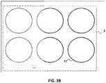
- FIG. 3B is a schematic view of a collimating assembly 3 in the display assembly 2.
- the collimating assembly 3 comprises a plurality of collimating units 31, each of the light emitting units 21 has a corresponding collimating unit 31.
- FIG. 3C is a schematic of the combination of FIG. 3A and FIG. 3B .
- Each diameter of the collimating units 31 is at least two time of a length of the first side d1 of the light emitting units 21; and a spacing L2 between each of the collimating units 31 is at least 400nm.
Landscapes
- Physics & Mathematics (AREA)
- Optics & Photonics (AREA)
- General Physics & Mathematics (AREA)
- Engineering & Computer Science (AREA)
- Microelectronics & Electronic Packaging (AREA)
- Nonlinear Science (AREA)
- Geometry (AREA)
- Liquid Crystal (AREA)
- Devices For Indicating Variable Information By Combining Individual Elements (AREA)
- Electroluminescent Light Sources (AREA)
Applications Claiming Priority (2)
| Application Number | Priority Date | Filing Date | Title |
|---|---|---|---|
| PCT/CN2018/077715 WO2019165620A1 (fr) | 2018-03-01 | 2018-03-01 | Procédé d'affichage proche de l'œil permettant une imagerie en champ multi-profondeur |
| PCT/CN2019/076752 WO2019166018A1 (fr) | 2018-03-01 | 2019-03-01 | Composant d'affichage et dispositif d'affichage |
Publications (2)
| Publication Number | Publication Date |
|---|---|
| EP3761364A1 true EP3761364A1 (fr) | 2021-01-06 |
| EP3761364A4 EP3761364A4 (fr) | 2021-04-21 |
Family
ID=67804822
Family Applications (2)
| Application Number | Title | Priority Date | Filing Date |
|---|---|---|---|
| EP18907507.0A Active EP3761102B1 (fr) | 2018-03-01 | 2018-03-01 | Procédé d'affichage proche de l'oeil permettant une imagerie en champ multi-profondeur |
| EP19760179.2A Withdrawn EP3761364A4 (fr) | 2018-03-01 | 2019-03-01 | Composant d'affichage et dispositif d'affichage |
Family Applications Before (1)
| Application Number | Title | Priority Date | Filing Date |
|---|---|---|---|
| EP18907507.0A Active EP3761102B1 (fr) | 2018-03-01 | 2018-03-01 | Procédé d'affichage proche de l'oeil permettant une imagerie en champ multi-profondeur |
Country Status (7)
| Country | Link |
|---|---|
| US (2) | US11927871B2 (fr) |
| EP (2) | EP3761102B1 (fr) |
| JP (2) | JP7195653B2 (fr) |
| KR (2) | KR20200127023A (fr) |
| CN (2) | CN111837068A (fr) |
| TW (1) | TW201937234A (fr) |
| WO (2) | WO2019165620A1 (fr) |
Families Citing this family (17)
| Publication number | Priority date | Publication date | Assignee | Title |
|---|---|---|---|---|
| WO2019165620A1 (fr) | 2018-03-01 | 2019-09-06 | 陈台国 | Procédé d'affichage proche de l'œil permettant une imagerie en champ multi-profondeur |
| JP7582675B2 (ja) | 2019-11-06 | 2024-11-13 | ヒーズ アイピー ホールディングス エルエルシー | 奥行きのある物体を表示するシステム及び方法 |
| CN110910769B (zh) * | 2019-11-29 | 2022-04-08 | 京东方科技集团股份有限公司 | 虚拟显示装置及其制备方法、控制方法 |
| EP4128355A4 (fr) | 2020-04-01 | 2024-04-10 | Massachusetts Institute of Technology | Systèmes fondés sur une méta-optique et procédés d'applications oculaires |
| EP4136496A4 (fr) | 2020-06-19 | 2024-07-10 | HES IP Holdings, LLC | Systèmes d'affichage d'image pour expansion de région oculaire et leurs procédés de fabrication |
| CN111864119B (zh) * | 2020-07-31 | 2024-01-19 | 京东方科技集团股份有限公司 | 显示器件和近眼显示设备 |
| TWI886046B (zh) | 2020-08-14 | 2025-06-01 | 英屬開曼群島商沃彌股份有限公司 | 用於產生具有深度的虛擬影像的虛擬影像模組 |
| EP4570162A3 (fr) | 2020-09-03 | 2025-09-03 | Oomii Inc. | Systèmes et procédés d'amélioration de la vision binoculaire |
| CN116194979B (zh) * | 2020-09-17 | 2025-07-29 | 夏普株式会社 | 显示装置及显示装置的制造方法 |
| US11953689B2 (en) | 2020-09-30 | 2024-04-09 | Hes Ip Holdings, Llc | Virtual image display system for virtual reality and augmented reality devices |
| JP2022097093A (ja) * | 2020-12-18 | 2022-06-30 | ソニーセミコンダクタソリューションズ株式会社 | 半導体装置 |
| JP7601521B2 (ja) | 2021-02-08 | 2024-12-17 | ヒーズ アイピー ホールディングス エルエルシー | 視力を高めるシステム及び方法 |
| KR102877541B1 (ko) | 2021-04-30 | 2025-10-29 | 삼성디스플레이 주식회사 | 표시 장치 |
| EP4204896A4 (fr) * | 2021-06-11 | 2024-09-25 | HES IP Holdings, LLC | Systèmes et méthodes pour améliorer la vision de l'oeil d'un observateur ayant une rétine déficiente |
| TWI832581B (zh) | 2021-12-15 | 2024-02-11 | 財團法人工業技術研究院 | 眼鏡上的頭戴式擴增實境立體視覺光學膜 |
| TWI807535B (zh) | 2021-12-15 | 2023-07-01 | 財團法人工業技術研究院 | 眼鏡上的頭戴式擴增實境立體視覺光學膜 |
| KR20250046273A (ko) * | 2022-08-09 | 2025-04-02 | 소니 세미컨덕터 솔루션즈 가부시키가이샤 | 발광 장치 및 전자 기기 |
Family Cites Families (44)
| Publication number | Priority date | Publication date | Assignee | Title |
|---|---|---|---|---|
| JP3136178B2 (ja) | 1991-10-09 | 2001-02-19 | 株式会社リコー | ディスプレイ装置 |
| JPH11234705A (ja) * | 1998-02-17 | 1999-08-27 | Matsushita Electric Ind Co Ltd | 立体表示装置 |
| JP2002090704A (ja) | 2000-09-18 | 2002-03-27 | Katsumi Yoshino | 液晶表示パネル読取装置 |
| JP4491948B2 (ja) * | 2000-10-06 | 2010-06-30 | ソニー株式会社 | 素子実装方法および画像表示装置の製造方法 |
| SG143945A1 (en) | 2001-02-19 | 2008-07-29 | Semiconductor Energy Lab | Light emitting device and method of manufacturing the same |
| JP2005175417A (ja) | 2003-07-28 | 2005-06-30 | Ricoh Co Ltd | 発光素子アレイ、光書込ユニットおよび画像形成装置 |
| JP2007027157A (ja) | 2005-07-12 | 2007-02-01 | Akita Denshi Systems:Kk | 発光ダイオード装置及びその製造方法並びに照明装置 |
| JP4839795B2 (ja) | 2005-11-24 | 2011-12-21 | ソニー株式会社 | 3次元表示装置 |
| US7782278B2 (en) * | 2006-12-14 | 2010-08-24 | Himax Technologies Limited | Intra-pixel convolution for AMOLED |
| JP2011145607A (ja) | 2010-01-18 | 2011-07-28 | Sony Corp | ヘッドマウントディスプレイ |
| US20130285885A1 (en) | 2012-04-25 | 2013-10-31 | Andreas G. Nowatzyk | Head-mounted light-field display |
| CN102629667B (zh) | 2012-04-25 | 2015-03-25 | 上海大学 | 硅基顶发射有机发光微显示器及其制备方法 |
| US9841537B2 (en) * | 2012-07-02 | 2017-12-12 | Nvidia Corporation | Near-eye microlens array displays |
| US9860522B2 (en) | 2012-08-04 | 2018-01-02 | Paul Lapstun | Head-mounted light field display |
| US20140056003A1 (en) | 2012-08-20 | 2014-02-27 | John Frattalone | Modular video and lighting displays |
| US9442460B2 (en) | 2012-10-31 | 2016-09-13 | Lg Display Co., Ltd. | Digital hologram display device |
| CN105008983B (zh) * | 2012-12-21 | 2018-08-07 | 瑞尔D斯帕克有限责任公司 | 用于定向显示器的超透镜组件 |
| JP6337433B2 (ja) | 2013-09-13 | 2018-06-06 | セイコーエプソン株式会社 | 頭部装着型表示装置および頭部装着型表示装置の制御方法 |
| KR102053440B1 (ko) * | 2013-09-26 | 2020-01-08 | 엘지디스플레이 주식회사 | 고 개구율 유기발광 다이오드 표시장치 및 그 제조 방법 |
| GB2525862A (en) | 2014-05-06 | 2015-11-11 | Univ Bedfordshire | Lens array and imaging device |
| JP6305855B2 (ja) | 2014-07-11 | 2018-04-04 | オリンパス株式会社 | 画像表示装置 |
| GB201413578D0 (en) | 2014-07-31 | 2014-09-17 | Infiniled Ltd | A colour iled display on silicon |
| GB201418772D0 (en) | 2014-10-22 | 2014-12-03 | Infiniled Ltd | Display |
| KR102312576B1 (ko) * | 2014-11-05 | 2021-10-14 | 엘지디스플레이 주식회사 | 유기전계발광표시장치 및 그 제조방법 |
| CN105739094A (zh) * | 2014-12-11 | 2016-07-06 | 北京邮电大学 | 一种基于透镜阵列的近眼显示方法 |
| WO2016163231A1 (fr) | 2015-04-09 | 2016-10-13 | シャープ株式会社 | Dispositif d'affichage de type lunettes |
| WO2017053309A1 (fr) | 2015-09-23 | 2017-03-30 | Osram Sylvania Inc. | Métalentilles de collimation et technologies les incorporant |
| FR3044467B1 (fr) | 2015-11-26 | 2018-08-10 | Commissariat A L'energie Atomique Et Aux Energies Alternatives | Dalle lumineuse et procede de fabrication d'une telle dalle lumineuse |
| CN105449125B (zh) | 2015-12-03 | 2018-11-09 | 东南大学 | 一种硅基量子点显示器及其制作方法 |
| TWI696847B (zh) | 2016-01-28 | 2020-06-21 | 中強光電股份有限公司 | 頭戴式顯示裝置 |
| US9964767B2 (en) | 2016-03-03 | 2018-05-08 | Google Llc | Display with reflected LED micro-display panels |
| WO2018013307A1 (fr) | 2016-06-21 | 2018-01-18 | Ntt Docomo, Inc. | Dispositif d'éclairage pour un dispositif d'affichage portable |
| CN107561702A (zh) | 2016-07-01 | 2018-01-09 | 成都理想境界科技有限公司 | 一种近眼显示系统、虚拟现实设备和增强现实设备 |
| CN107561697B (zh) | 2016-07-01 | 2019-04-30 | 成都理想境界科技有限公司 | 近眼显示系统、虚拟现实设备及增强现实设备 |
| CN105911791A (zh) | 2016-07-04 | 2016-08-31 | 京东方科技集团股份有限公司 | 一种显示面板及显示装置 |
| CN107664840A (zh) | 2016-07-28 | 2018-02-06 | 中强光电股份有限公司 | 头戴式显示装置 |
| CN106057843B (zh) | 2016-08-05 | 2019-04-30 | 京东方科技集团股份有限公司 | 透明显示面板、透明显示装置及透明显示面板的制作方法 |
| TWI607243B (zh) | 2016-08-09 | 2017-12-01 | Tai Guo Chen | Display adjustment method for near-eye display |
| CN106292240A (zh) | 2016-09-05 | 2017-01-04 | 京东方科技集团股份有限公司 | 全息显示装置及其显示方法 |
| CN106526864B (zh) * | 2017-01-05 | 2019-08-30 | 京东方科技集团股份有限公司 | 显示装置和显示方法 |
| CN106873161B (zh) | 2017-03-02 | 2020-03-17 | 上海天马微电子有限公司 | 一种显示装置及近眼可穿戴设备 |
| CN107490862B (zh) | 2017-03-23 | 2019-10-25 | 华为机器有限公司 | 近眼显示器及近眼显示系统 |
| CN106932916B (zh) * | 2017-05-04 | 2019-10-01 | 鲁东大学 | 一种利用超材料透镜的双光束超分辨聚焦方法 |
| WO2019165620A1 (fr) | 2018-03-01 | 2019-09-06 | 陈台国 | Procédé d'affichage proche de l'œil permettant une imagerie en champ multi-profondeur |
-
2018
- 2018-03-01 WO PCT/CN2018/077715 patent/WO2019165620A1/fr not_active Ceased
- 2018-03-01 JP JP2020568582A patent/JP7195653B2/ja active Active
- 2018-03-01 KR KR1020207028341A patent/KR20200127023A/ko not_active Ceased
- 2018-03-01 CN CN201880090627.7A patent/CN111837068A/zh active Pending
- 2018-03-01 EP EP18907507.0A patent/EP3761102B1/fr active Active
- 2018-03-01 US US16/976,506 patent/US11927871B2/en active Active
-
2019
- 2019-02-28 TW TW108106943A patent/TW201937234A/zh unknown
- 2019-03-01 US US16/976,526 patent/US20210005681A1/en not_active Abandoned
- 2019-03-01 JP JP2020568586A patent/JP2021520523A/ja active Pending
- 2019-03-01 EP EP19760179.2A patent/EP3761364A4/fr not_active Withdrawn
- 2019-03-01 CN CN201980016537.8A patent/CN111801803A/zh active Pending
- 2019-03-01 KR KR1020207028337A patent/KR20200127235A/ko not_active Ceased
- 2019-03-01 WO PCT/CN2019/076752 patent/WO2019166018A1/fr not_active Ceased
Also Published As
| Publication number | Publication date |
|---|---|
| CN111801803A (zh) | 2020-10-20 |
| US20210005681A1 (en) | 2021-01-07 |
| JP2021520523A (ja) | 2021-08-19 |
| EP3761102B1 (fr) | 2023-11-29 |
| JP2021521494A (ja) | 2021-08-26 |
| US20210003900A1 (en) | 2021-01-07 |
| US11927871B2 (en) | 2024-03-12 |
| EP3761364A4 (fr) | 2021-04-21 |
| EP3761102A4 (fr) | 2021-10-27 |
| CN111837068A (zh) | 2020-10-27 |
| EP3761102A1 (fr) | 2021-01-06 |
| JP7195653B2 (ja) | 2022-12-26 |
| WO2019166018A1 (fr) | 2019-09-06 |
| KR20200127235A (ko) | 2020-11-10 |
| WO2019165620A1 (fr) | 2019-09-06 |
| KR20200127023A (ko) | 2020-11-09 |
| TW201937234A (zh) | 2019-09-16 |
Similar Documents
| Publication | Publication Date | Title |
|---|---|---|
| EP3761364A1 (fr) | Composant d'affichage et dispositif d'affichage | |
| TWI697693B (zh) | 多光束元件式近眼顯示器、系統、與方法 | |
| KR102563214B1 (ko) | 핀포인트 미러를 갖는 증강 현실 광학 시스템 | |
| US9726887B2 (en) | Imaging structure color conversion | |
| US9684174B2 (en) | Imaging structure with embedded light sources | |
| US9779643B2 (en) | Imaging structure emitter configurations | |
| US8582209B1 (en) | Curved near-to-eye display | |
| US20140043320A1 (en) | Beamed-Pixel Retinal Displays | |
| TW201736874A (zh) | 多光束繞射格柵式近眼顯示器 | |
| TWI691739B (zh) | 具有多重景深顯像的近眼顯示方法 | |
| CN110850595B (zh) | 光学设备 | |
| US20250138317A1 (en) | Near-eye display apparatus, display method thereof and wearable device | |
| KR20240125701A (ko) | 마이크로 led 디스플레이 디바이스 | |
| CN118613856A (zh) | 微型led投影器 | |
| KR102687455B1 (ko) | 개인 몰입형 광학장치, 표시패널 및 표시장치 | |
| US20240255759A1 (en) | Near-eye display device | |
| US10957240B1 (en) | Apparatus, systems, and methods to compensate for sub-standard sub pixels in an array | |
| US20210231956A1 (en) | Display device and augmented reality apparatus including the same | |
| JP2025066621A (ja) | コリメート機能付きコンタクトレンズおよびxrグラス | |
| CN118859524A (zh) | 一种光场显示装置及可穿戴设备 |
Legal Events
| Date | Code | Title | Description |
|---|---|---|---|
| STAA | Information on the status of an ep patent application or granted ep patent |
Free format text: STATUS: THE INTERNATIONAL PUBLICATION HAS BEEN MADE |
|
| PUAI | Public reference made under article 153(3) epc to a published international application that has entered the european phase |
Free format text: ORIGINAL CODE: 0009012 |
|
| STAA | Information on the status of an ep patent application or granted ep patent |
Free format text: STATUS: REQUEST FOR EXAMINATION WAS MADE |
|
| 17P | Request for examination filed |
Effective date: 20200930 |
|
| AK | Designated contracting states |
Kind code of ref document: A1 Designated state(s): AL AT BE BG CH CY CZ DE DK EE ES FI FR GB GR HR HU IE IS IT LI LT LU LV MC MK MT NL NO PL PT RO RS SE SI SK SM TR |
|
| AX | Request for extension of the european patent |
Extension state: BA ME |
|
| A4 | Supplementary search report drawn up and despatched |
Effective date: 20210323 |
|
| RIC1 | Information provided on ipc code assigned before grant |
Ipc: H01L 25/075 20060101AFI20210317BHEP Ipc: H01L 25/16 20060101ALI20210317BHEP Ipc: H01L 33/58 20100101ALN20210317BHEP |
|
| DAV | Request for validation of the european patent (deleted) | ||
| DAX | Request for extension of the european patent (deleted) | ||
| STAA | Information on the status of an ep patent application or granted ep patent |
Free format text: STATUS: EXAMINATION IS IN PROGRESS |
|
| 17Q | First examination report despatched |
Effective date: 20220613 |
|
| STAA | Information on the status of an ep patent application or granted ep patent |
Free format text: STATUS: THE APPLICATION HAS BEEN WITHDRAWN |
|
| 18W | Application withdrawn |
Effective date: 20221117 |