EP3761464B1 - Laser à cavité verticale émettant en surface segmentée - Google Patents
Laser à cavité verticale émettant en surface segmentée Download PDFInfo
- Publication number
- EP3761464B1 EP3761464B1 EP20184734.0A EP20184734A EP3761464B1 EP 3761464 B1 EP3761464 B1 EP 3761464B1 EP 20184734 A EP20184734 A EP 20184734A EP 3761464 B1 EP3761464 B1 EP 3761464B1
- Authority
- EP
- European Patent Office
- Prior art keywords
- layer
- guiding structure
- bragg reflector
- cavity surface
- vertical cavity
- Prior art date
- Legal status (The legal status is an assumption and is not a legal conclusion. Google has not performed a legal analysis and makes no representation as to the accuracy of the status listed.)
- Active
Links
Images



Classifications
-
- H—ELECTRICITY
- H01—ELECTRIC ELEMENTS
- H01S—DEVICES USING THE PROCESS OF LIGHT AMPLIFICATION BY STIMULATED EMISSION OF RADIATION [LASER] TO AMPLIFY OR GENERATE LIGHT; DEVICES USING STIMULATED EMISSION OF ELECTROMAGNETIC RADIATION IN WAVE RANGES OTHER THAN OPTICAL
- H01S5/00—Semiconductor lasers
- H01S5/10—Construction or shape of the optical resonator, e.g. extended or external cavity, coupled cavities, bent-guide, varying width, thickness or composition of the active region
- H01S5/18—Surface-emitting [SE] lasers, e.g. having both horizontal and vertical cavities
- H01S5/183—Surface-emitting [SE] lasers, e.g. having both horizontal and vertical cavities having only vertical cavities, e.g. vertical cavity surface-emitting lasers [VCSEL]
- H01S5/18308—Surface-emitting [SE] lasers, e.g. having both horizontal and vertical cavities having only vertical cavities, e.g. vertical cavity surface-emitting lasers [VCSEL] having a special structure for lateral current or light confinement
- H01S5/18319—Surface-emitting [SE] lasers, e.g. having both horizontal and vertical cavities having only vertical cavities, e.g. vertical cavity surface-emitting lasers [VCSEL] having a special structure for lateral current or light confinement comprising a periodical structure in lateral directions
-
- H—ELECTRICITY
- H01—ELECTRIC ELEMENTS
- H01S—DEVICES USING THE PROCESS OF LIGHT AMPLIFICATION BY STIMULATED EMISSION OF RADIATION [LASER] TO AMPLIFY OR GENERATE LIGHT; DEVICES USING STIMULATED EMISSION OF ELECTROMAGNETIC RADIATION IN WAVE RANGES OTHER THAN OPTICAL
- H01S5/00—Semiconductor lasers
- H01S5/04—Processes or apparatus for excitation, e.g. pumping, e.g. by electron beams
- H01S5/042—Electrical excitation ; Circuits therefor
- H01S5/0421—Electrical excitation ; Circuits therefor characterised by the semiconducting contacting layers
-
- H—ELECTRICITY
- H01—ELECTRIC ELEMENTS
- H01S—DEVICES USING THE PROCESS OF LIGHT AMPLIFICATION BY STIMULATED EMISSION OF RADIATION [LASER] TO AMPLIFY OR GENERATE LIGHT; DEVICES USING STIMULATED EMISSION OF ELECTROMAGNETIC RADIATION IN WAVE RANGES OTHER THAN OPTICAL
- H01S5/00—Semiconductor lasers
- H01S5/06—Arrangements for controlling the laser output parameters, e.g. by operating on the active medium
- H01S5/062—Arrangements for controlling the laser output parameters, e.g. by operating on the active medium by varying the potential of the electrodes
- H01S5/06203—Transistor-type lasers
-
- H—ELECTRICITY
- H01—ELECTRIC ELEMENTS
- H01S—DEVICES USING THE PROCESS OF LIGHT AMPLIFICATION BY STIMULATED EMISSION OF RADIATION [LASER] TO AMPLIFY OR GENERATE LIGHT; DEVICES USING STIMULATED EMISSION OF ELECTROMAGNETIC RADIATION IN WAVE RANGES OTHER THAN OPTICAL
- H01S5/00—Semiconductor lasers
- H01S5/10—Construction or shape of the optical resonator, e.g. extended or external cavity, coupled cavities, bent-guide, varying width, thickness or composition of the active region
- H01S5/18—Surface-emitting [SE] lasers, e.g. having both horizontal and vertical cavities
- H01S5/183—Surface-emitting [SE] lasers, e.g. having both horizontal and vertical cavities having only vertical cavities, e.g. vertical cavity surface-emitting lasers [VCSEL]
- H01S5/18305—Surface-emitting [SE] lasers, e.g. having both horizontal and vertical cavities having only vertical cavities, e.g. vertical cavity surface-emitting lasers [VCSEL] with emission through the substrate, i.e. bottom emission
-
- H—ELECTRICITY
- H01—ELECTRIC ELEMENTS
- H01S—DEVICES USING THE PROCESS OF LIGHT AMPLIFICATION BY STIMULATED EMISSION OF RADIATION [LASER] TO AMPLIFY OR GENERATE LIGHT; DEVICES USING STIMULATED EMISSION OF ELECTROMAGNETIC RADIATION IN WAVE RANGES OTHER THAN OPTICAL
- H01S5/00—Semiconductor lasers
- H01S5/10—Construction or shape of the optical resonator, e.g. extended or external cavity, coupled cavities, bent-guide, varying width, thickness or composition of the active region
- H01S5/18—Surface-emitting [SE] lasers, e.g. having both horizontal and vertical cavities
- H01S5/183—Surface-emitting [SE] lasers, e.g. having both horizontal and vertical cavities having only vertical cavities, e.g. vertical cavity surface-emitting lasers [VCSEL]
- H01S5/18308—Surface-emitting [SE] lasers, e.g. having both horizontal and vertical cavities having only vertical cavities, e.g. vertical cavity surface-emitting lasers [VCSEL] having a special structure for lateral current or light confinement
-
- H—ELECTRICITY
- H01—ELECTRIC ELEMENTS
- H01S—DEVICES USING THE PROCESS OF LIGHT AMPLIFICATION BY STIMULATED EMISSION OF RADIATION [LASER] TO AMPLIFY OR GENERATE LIGHT; DEVICES USING STIMULATED EMISSION OF ELECTROMAGNETIC RADIATION IN WAVE RANGES OTHER THAN OPTICAL
- H01S5/00—Semiconductor lasers
- H01S5/10—Construction or shape of the optical resonator, e.g. extended or external cavity, coupled cavities, bent-guide, varying width, thickness or composition of the active region
- H01S5/18—Surface-emitting [SE] lasers, e.g. having both horizontal and vertical cavities
- H01S5/183—Surface-emitting [SE] lasers, e.g. having both horizontal and vertical cavities having only vertical cavities, e.g. vertical cavity surface-emitting lasers [VCSEL]
- H01S5/18308—Surface-emitting [SE] lasers, e.g. having both horizontal and vertical cavities having only vertical cavities, e.g. vertical cavity surface-emitting lasers [VCSEL] having a special structure for lateral current or light confinement
- H01S5/18311—Surface-emitting [SE] lasers, e.g. having both horizontal and vertical cavities having only vertical cavities, e.g. vertical cavity surface-emitting lasers [VCSEL] having a special structure for lateral current or light confinement using selective oxidation
-
- H—ELECTRICITY
- H01—ELECTRIC ELEMENTS
- H01S—DEVICES USING THE PROCESS OF LIGHT AMPLIFICATION BY STIMULATED EMISSION OF RADIATION [LASER] TO AMPLIFY OR GENERATE LIGHT; DEVICES USING STIMULATED EMISSION OF ELECTROMAGNETIC RADIATION IN WAVE RANGES OTHER THAN OPTICAL
- H01S5/00—Semiconductor lasers
- H01S5/10—Construction or shape of the optical resonator, e.g. extended or external cavity, coupled cavities, bent-guide, varying width, thickness or composition of the active region
- H01S5/18—Surface-emitting [SE] lasers, e.g. having both horizontal and vertical cavities
- H01S5/183—Surface-emitting [SE] lasers, e.g. having both horizontal and vertical cavities having only vertical cavities, e.g. vertical cavity surface-emitting lasers [VCSEL]
- H01S5/18308—Surface-emitting [SE] lasers, e.g. having both horizontal and vertical cavities having only vertical cavities, e.g. vertical cavity surface-emitting lasers [VCSEL] having a special structure for lateral current or light confinement
- H01S5/18311—Surface-emitting [SE] lasers, e.g. having both horizontal and vertical cavities having only vertical cavities, e.g. vertical cavity surface-emitting lasers [VCSEL] having a special structure for lateral current or light confinement using selective oxidation
- H01S5/18313—Surface-emitting [SE] lasers, e.g. having both horizontal and vertical cavities having only vertical cavities, e.g. vertical cavity surface-emitting lasers [VCSEL] having a special structure for lateral current or light confinement using selective oxidation by oxidizing at least one of the DBR layers
-
- H—ELECTRICITY
- H01—ELECTRIC ELEMENTS
- H01S—DEVICES USING THE PROCESS OF LIGHT AMPLIFICATION BY STIMULATED EMISSION OF RADIATION [LASER] TO AMPLIFY OR GENERATE LIGHT; DEVICES USING STIMULATED EMISSION OF ELECTROMAGNETIC RADIATION IN WAVE RANGES OTHER THAN OPTICAL
- H01S5/00—Semiconductor lasers
- H01S5/10—Construction or shape of the optical resonator, e.g. extended or external cavity, coupled cavities, bent-guide, varying width, thickness or composition of the active region
- H01S5/18—Surface-emitting [SE] lasers, e.g. having both horizontal and vertical cavities
- H01S5/183—Surface-emitting [SE] lasers, e.g. having both horizontal and vertical cavities having only vertical cavities, e.g. vertical cavity surface-emitting lasers [VCSEL]
- H01S5/18308—Surface-emitting [SE] lasers, e.g. having both horizontal and vertical cavities having only vertical cavities, e.g. vertical cavity surface-emitting lasers [VCSEL] having a special structure for lateral current or light confinement
- H01S5/18322—Position of the structure
-
- H—ELECTRICITY
- H01—ELECTRIC ELEMENTS
- H01S—DEVICES USING THE PROCESS OF LIGHT AMPLIFICATION BY STIMULATED EMISSION OF RADIATION [LASER] TO AMPLIFY OR GENERATE LIGHT; DEVICES USING STIMULATED EMISSION OF ELECTROMAGNETIC RADIATION IN WAVE RANGES OTHER THAN OPTICAL
- H01S5/00—Semiconductor lasers
- H01S5/10—Construction or shape of the optical resonator, e.g. extended or external cavity, coupled cavities, bent-guide, varying width, thickness or composition of the active region
- H01S5/18—Surface-emitting [SE] lasers, e.g. having both horizontal and vertical cavities
- H01S5/183—Surface-emitting [SE] lasers, e.g. having both horizontal and vertical cavities having only vertical cavities, e.g. vertical cavity surface-emitting lasers [VCSEL]
- H01S5/18308—Surface-emitting [SE] lasers, e.g. having both horizontal and vertical cavities having only vertical cavities, e.g. vertical cavity surface-emitting lasers [VCSEL] having a special structure for lateral current or light confinement
- H01S5/18322—Position of the structure
- H01S5/18327—Structure being part of a DBR
-
- H—ELECTRICITY
- H01—ELECTRIC ELEMENTS
- H01S—DEVICES USING THE PROCESS OF LIGHT AMPLIFICATION BY STIMULATED EMISSION OF RADIATION [LASER] TO AMPLIFY OR GENERATE LIGHT; DEVICES USING STIMULATED EMISSION OF ELECTROMAGNETIC RADIATION IN WAVE RANGES OTHER THAN OPTICAL
- H01S5/00—Semiconductor lasers
- H01S5/10—Construction or shape of the optical resonator, e.g. extended or external cavity, coupled cavities, bent-guide, varying width, thickness or composition of the active region
- H01S5/18—Surface-emitting [SE] lasers, e.g. having both horizontal and vertical cavities
- H01S5/183—Surface-emitting [SE] lasers, e.g. having both horizontal and vertical cavities having only vertical cavities, e.g. vertical cavity surface-emitting lasers [VCSEL]
- H01S5/18361—Structure of the reflectors, e.g. hybrid mirrors
-
- H—ELECTRICITY
- H01—ELECTRIC ELEMENTS
- H01S—DEVICES USING THE PROCESS OF LIGHT AMPLIFICATION BY STIMULATED EMISSION OF RADIATION [LASER] TO AMPLIFY OR GENERATE LIGHT; DEVICES USING STIMULATED EMISSION OF ELECTROMAGNETIC RADIATION IN WAVE RANGES OTHER THAN OPTICAL
- H01S5/00—Semiconductor lasers
- H01S5/10—Construction or shape of the optical resonator, e.g. extended or external cavity, coupled cavities, bent-guide, varying width, thickness or composition of the active region
- H01S5/18—Surface-emitting [SE] lasers, e.g. having both horizontal and vertical cavities
- H01S5/183—Surface-emitting [SE] lasers, e.g. having both horizontal and vertical cavities having only vertical cavities, e.g. vertical cavity surface-emitting lasers [VCSEL]
- H01S5/18383—Surface-emitting [SE] lasers, e.g. having both horizontal and vertical cavities having only vertical cavities, e.g. vertical cavity surface-emitting lasers [VCSEL] with periodic active regions at nodes or maxima of light intensity
-
- H—ELECTRICITY
- H01—ELECTRIC ELEMENTS
- H01S—DEVICES USING THE PROCESS OF LIGHT AMPLIFICATION BY STIMULATED EMISSION OF RADIATION [LASER] TO AMPLIFY OR GENERATE LIGHT; DEVICES USING STIMULATED EMISSION OF ELECTROMAGNETIC RADIATION IN WAVE RANGES OTHER THAN OPTICAL
- H01S5/00—Semiconductor lasers
- H01S5/10—Construction or shape of the optical resonator, e.g. extended or external cavity, coupled cavities, bent-guide, varying width, thickness or composition of the active region
- H01S5/18—Surface-emitting [SE] lasers, e.g. having both horizontal and vertical cavities
- H01S5/183—Surface-emitting [SE] lasers, e.g. having both horizontal and vertical cavities having only vertical cavities, e.g. vertical cavity surface-emitting lasers [VCSEL]
- H01S5/18386—Details of the emission surface for influencing the near- or far-field, e.g. a grating on the surface
Definitions
- the invention relates to a segmented Vertical Cavity Surface Emitting Laser (VCSEL) device comprising a guiding structure arranged to provide separated optical modes.
- the invention further relates to an optical sensor comprising such a VCSEL device and a mobile communication device comprising such an optical sensor.
- the invention further relates to a corresponding method of fabricating such a VCSEL device.
- VCSEL Vertical Cavity Surface Emitting Laser
- Addressable arrays of VCSELs are of increasing importance in the field of sensors for depth imaging as well as for printing/additive manufacturing. Depending on the application it cannot be tolerated if one single pixel fails. Such a single pixel failure would cause a total device failure. This makes pixelated arrays comprising large VCSELs (large light emitting area) unfavorable because the rate of single pixel failures increases with the size of the VCSEL.
- US 2017/0302059 A1 discloses a VCSEL and a method of manufacturing such a VCSEL.
- the VCSEL comprises a first electrical contact, a substrate, a first distributed Bragg reflector, an active layer, a distributed heterojunction bipolar phototransistor, a second distributed Bragg reflector and a second electrical contact, the distributed heterojunction bipolar phototransistor comprising a collector layer, a light sensitive layer, a base layer and an emitter layer, wherein the distributed heterojunction bipolar phototransistor is arranged such that there is an optical coupling between the active layer and the distributed heterojunction bipolar phototransistor for providing an active carrier confinement by means of the distributed heterojunction bipolar phototransistor such that an optical mode of the VCSEL is self-positioning in accordance with the active carrier confinement during operation of the VCSEL.
- US 6,061,381 A discloses a VCSEL which includes a resonant cavity formed between a distributed Bragg reflector formed of semiconductor material and an overlying distributed Bragg reflector formed of dielectric material.
- the resonant cavity contains a layer of laser active material sandwiched between spacer layers and a blocking layer which confines an energizing electric current to flow through the cavity between a metallic contact layer on the underside of the Bragg reflector and another contact.
- a series of concentric rings is formed in the blocking layer surrounding the resonant cavity so as to provide a Bragg structure which reflects light from the cavity with a phase characteristic that supports the preselected transverse resonant mode.
- EP 1 501 162 A2 discloses a phase array of oxide confined VCSELs and a method for forming the phase array of oxide confined VCSELs is described.
- VCSELs in the array are designed to be simultaneously addressed such that the output of multiple VCSELs can be used to increase the light intensity at a point.
- high gain coupling regions break the continuity of the oxide wall surrounding each VCSEL aperture. The high gain coupling regions connect adjacent VCSELs in the VCSEL array thereby allowing mode coupling between adjacent lasers and the output of a coherent beam of light.
- WO 2008/043526 A1 discloses a vertical cavity surface emitting optical device that has an optical confinement structure, such as the top electrode, which is specially shaped to provide an optical output that has a shape orthogonal to the beam axis of the optical device which shape is substantially non-circular, e.g. polygonal, so as to enable direct projection of predetermined, complex shapes and patterns of light in the form of letters, numbers, symbols, logos, trademarks and other information bearing patterns.
- a VCSEL device as defined in claim 1 is provided.
- Lasing is inhibited in between the two, three, four or more light emitting areas.
- the two, three, four or more in a relative intensity maxima are separated or to be more precise essentially independent from each other.
- Different optical modes may contribute to the relative intensity maxima at different lateral positions.
- the guiding structure may be arranged to reduce an intensity of at least one optical mode contributing to at least one of the first or second relative intensity maximum outside the at least the first or the second light emitting area such that a lateral extension of the light emitting areas is bound to the respective lateral position of the optical resonator.
- the first and the second electrical contact are arranged to electrically pump the active layer.
- the first or the second reflecting structure may comprise reflective elements which are not comprised by the first or the second DBR contributing to the total reflectivity of the first or second reflecting structure.
- the active layer may comprise two, three, four or more light-emitting areas across the lateral extension of the active layer which defined by means of the guiding structure.
- the layer stack of the optical resonator arranged on the first side of the substrate is characterized by a thickness of between 5-20 ⁇ m.
- the substrate is usually characterized by thickness of between 100-600 ⁇ m such that a second side of the substrate opposing the first side is separated from the first side by at least 100 ⁇ m.
- VECSEL Vertical External Cavity Surface Emitting Lasers
- layer does not exclude that the layer comprises two or more sub-layers.
- Addressable arrays of VCSELs or VCSEL devices are of increasing importance in the field of sensors for depth imaging as well as for printing/additive manufacturing. Depending on the application it cannot be tolerated if one single pixel fails. Such a failure would cause a total device failure.
- VCSELs devices can fail because defects develop in the crystal, which absorb part of the laser radiation and drive up the laser threshold. By such absorption the local temperature at the defect region increases and the defects grow, leading to even higher absorption and finally a total failure.
- each element of the array (VCSEL with small active area) is imaged by the help of optics onto a single pixel in the application. This requires a significant effort and space which is not feasible for mass applications.
- Especially bottom emitting VCSELs devices emitting laser light through the substrate with a full metal anode contact can be scaled to relatively large diameter (total active area of more than 200 ⁇ m 2 , more preferably more than 400 ⁇ m 2 and most preferably more than 600 ⁇ m 2 ) in order to enable higher power applications.
- Flip-chip mounting of the bottom emitter on an electronic driver allows individual "pixel" addressing.
- Such architecture is most compact but not used today because of the reliability issue discussed above.
- the VCSEL device according to claim 1 enables making of a large area VCSEL device with an optical separation of different light emitting areas across the aperture. Relative maxima of the intensity distribution stay in defined parts of the aperture or active area and do not intermix.
- An advantage of separation of light emitting areas across the lateral extension of the active area of the connected active layer is that a single region of such a light emitting area failing will cause the respective light emitting area of the device to stop lasing. Therefore the optical intensity in this region is reduced (and because of the separation other regions do not bring in their intensity) and local heating by absorption is avoided. The defect will not propagate further and the damage remains localized.
- the intensity distribution is therefore such that there is essentially no energy transfer between especially neighboring light-emitting areas and the corresponding relative intensity maxima.
- Each relative intensity maxima and contributing optical mode or modes gets the majority of its gain from the associated lateral position within the optical resonator (position of the associated light emitting area) and only minority from neighboring regions.
- a size of the light-emitting areas is at least 3 ⁇ m 2 .
- the light emitting areas are comprised by an active area of the active layer of at least 200 ⁇ m 2 .
- the guiding structure comprises a multitude of layers interacting such that separated relative intensity maxima of two, three, four or more light-emitting areas are bound to the respective location in the optical resonator.
- the guiding structure is arranged inside a layer stack of the first distributed Bragg reflector or the second distributed Bragg reflector in a vertical direction of the Vertical Cavity Surface Emitting Layer device.
- the vertical direction refers to a vertical direction of the vertical cavity of the Vertical Cavity Surface Emitting Laser device.
- the guiding structure is arranged within and (fully) enclosed by the optical resonator In a preferred embodiment, the guiding structure is arranged within and completely surrounded by the optical resonator In a preferred embodiment, the guiding structure is arranged inside the optical resonator, in particular inside the first DBR or inside the second DBR. In a preferred embodiment, the guiding structure is arranged within and fully enclosed by the first DBR or the second DBR. In a preferred embodiment, the guiding structure is arranged within a layer stack of the first DBR or the second DBR such that the optical guiding structure is surrounded of encapsulated by the first or the second DBR.
- An advantage of this approach may be a more homogeneous growth process of adjacent layers, e.g.
- the guiding structure is arranged such that at least one layer (or a sequence of at least two layers) of the layer stack of the first and/or second DBR is arranged in contact with the guiding structure and wherein and wherein said DBR layer or layer sequence in contact with the guiding structure is arranged in a vertical direction of the vertical cavity of the Vertical Cavity Surface Emitting Laser.
- At least a first layer of the first DBR is arranged above the guiding structure in a vertical direction of the vertical cavity of the Vertical Cavity Surface Emitting Laser and at least a second layer of the first DBR is arranged below the guiding structure in a vertical direction of the vertical cavity of the Vertical Cavity Surface Emitting Laser.
- the same may apply for the second DBR.
- An advantage of the guiding structure being arranged within (inside) a layer stack of the first DBR or the second DBR can be an improved structural integrity of the device.
- the device may be better suited for harsh application scenarios, more stable regarding vibrations and/or may offer an improve reliability for example in automotive applications.
- a (single) mesa structure may be provided that comprises the guiding structure rather than providing separate mesas that a separated by trenches and/or electrical contacts in between the separate mesas.
- the guiding structure is, for example, arranged to provide a lateral variation of a reflectivity of the first reflecting structure or the second reflecting structure parallel to the active layer.
- the guiding structure additionally comprises a variation of a thickness of at least one layer of the first DBR reflector or the second DBR
- the guiding structure in addition comprises a lateral variation of a reflectivity of the first electrical contact or the second electrical contact.
- the guiding structure comprises oxidized regions within more than one layer of the first distributed Bragg reflector or the second distributed Bragg reflector.
- the oxidized region are arranged to reduce the intensity in between the at least two light-emitting areas.
- the oxidized region is arranged to change the resonance conditions within the optical resonator in a lateral direction and/or to provide a local current confinement of the electrical current at the locations of the light emitting areas.
- the oxidized region may, for example, be arranged within an oxide aperture surrounding the at least two light emitting areas.
- the optical resonator further comprises a phototransistor (PT) or distributed heterojunction bipolar phototransistor (HPT).
- the HPT comprises a collector layer, a light sensitive layer, a base layer and an emitter layer.
- the HPT is arranged such that there is an optical coupling between the active layer and the HPT for providing an active carrier confinement by means of the HPT.
- the usage of a (monolithically integrated) HPT especially close to the active layer enables an efficient charge carrier confinement by controlling the carrier injection as a function of the local intensity of the actual profile of the lasing mode which is influenced by optical guiding provided by means of the optical guiding structure.
- the carrier injection may be adapted locally to the demand of the lasing mode and vice versa.
- the HPT effectively acts as a current confinement layer or structure.
- the advantage of the addition of the phototransistor is that it turns a slight optical modulation into a strong differentiation of lasing and non-lasing areas and inhibits current flow in between the segmented regions thus increasing efficiency.
- the HPT therefore supports the separation of the optical modes by amplifying, for example, slight optical guiding provided by the guiding structure.
- the HPT with optical sensitive collector-base junction may be designed to avoid optical absorption.
- the light sensitive layer may be a quantum well layer or a bulk layer.
- Bulk layers are, for example, homogeneous layers with a thickness of 10 nm or more in which quantum mechanic effects can be neglected.
- the HPT is arranged within the VCSEL such that the sensitivity with respect to light which is generated by means of the active layer of the VCSEL in combination with the optical resonator provided by the first and second DBR is sufficiently high.
- the HPT may, for example, be a pnp HPT which is arranged directly above the active layer meaning at the side of the active layer which is turned away from the usually n-conducting substrate.
- the layer structure of the HPT may even be integrated in one of the DBRs.
- the thickness of one or more of the HPT layers may be adapted to the emission wavelength of the VCSEL (quarter wavelength layer) in the respective material.
- One or more layers of the HPT may in this case be used to increase the reflectivity of the respective DBR. It may even be possible to use two HPTs one below and one above the active layer.
- Positioning of the HPT directly above or below the active layer may have the advantage that due to the low lateral conductivity between the HPT and the active layer the optical mode fits best to the profile of the respective charge carriers.
- the concentration of dopants in the collector layer, the base layer and the emitter layer may be less than 10 19 cm -3 .
- the dopants of the layers of the HPT cause optical losses such that a low doping level is preferred.
- the emitter layer of the HPT is the layer with the highest doping concentration.
- the concentration of dopants in the emitter layer may be, for example as low as 5*10 18 cm -3 or even 2*10 18 cm -3 .
- the concentration of dopants may be as low as 1*10 18 cm -3 in the base layer and 4*10 17 cm -3 in the collector layer in case of a concentration of dopants of 2*10 18 cm -3 in the emitter layer in order to reduce optical losses by means of the charge carriers.
- the thickness of the base layer may be 100 nm or less.
- the HPT may be a pnp HPT which is arranged between the active layer and the second DBR.
- the base layer may in this case have a thickness of around ⁇ /4 of the emission wavelength of the VCSEL in the material of the base layer.
- the emission wavelength may depend on the material of the substrate.
- a GaAs substrate may be used for an emission wavelength between 650 nm and around 1600 nm.
- a VCSEL with an InP substrate may emit laser light at an emission wavelength of more than or even much more than 1500 nm.
- the thickness of the collector layer may be in the range of ⁇ /2 of the emission wavelength of the VCSEL in the material.
- the guiding structure may be arranged outside a current flow which can be provided by means of the first electrical contact and the second electrical contact during operation of the VCSEL device.
- Optical confinement by means of the guiding structure does not directly interact with the current confinement provided by means of the HPT.
- the current flow is not disturbed by means of the guiding structure.
- the guiding structure may, for example, be arranged to provide across the lateral cross section of the optical resonator regions with an effective optical length enabling resonant laser operation intermitted by regions with a different effective optical length inhibiting laser operation.
- the guiding structure is arranged to reduce the effective optical length of the optical resonator at the regions where resonant laser operation is inhibited.
- a reduction of the effective optical lengths is enabled by local oxidization of more than one layer of the first or the second DBR as described above.
- the guiding structure may alternatively or in addition be arranged to increase the effective optical length of the optical resonator at the regions where resonant laser operation is enabled.
- An additional structured layer e.g. SiO 2 or SiN x
- a thickness of one or more semiconductor layer e.g. one or more Al y Ga (1-y) As-layer
- the guiding structure may be embedded in the layer structure of the first or second DBR.
- the corresponding DBR may in this case be a dielectric DBR comprising pairs of non-conducting dielectric layers with different refractive indices as, for example, Nb 2 O 5 , TiO 2 , TaO 2 , Si 3 N 4 and SiO 2 layers.
- the guiding structure may alternatively or in addition be arranged to provide a local current confinement at the at least two light-emitting areas.
- the guiding structure may, for example, additionally comprise the first or the second electrode, wherein the first or the second electrode is arranged to induce an electrically current distribution in accordance with the intensity distribution across the active layer.
- the first or second electrode may, for example, be structured in order to enable local current induction.
- the guiding structure may in addition comprise at least one layer with reduced lateral electrical conductivity in areas corresponding to an area of decreased intensity in between the at least two light-emitting areas.
- a doping profile of one or more semiconductor layer may, for example, be arranged such that electrical conductivity to the light emitting areas is increased and electrical conductivity of the areas between the light emitting areas is decreased.
- the VCSEL device may be arranged to emit laser light through the substrate (bottom emitter). Bottom emitters enable rather large active areas as described above.
- the bottom emitter or the optical resonator may comprise an extended optical cavity across the substrate.
- the guiding structure may comprise a lateral structuring of a second side of the substrate opposing the first side of the substrate.
- the guiding structure may alternatively or in addition comprise further layers deposited on the second side of the substrate supporting guiding of the separate relative intensity maxima (providing a lateral variation of optical feedback within the extended optical cavity).
- the VCSEL device is comprised by an optical sensor.
- the optical sensor is comprised by a mobile communication device.
- the optical sensor may alternatively be used in automotive applications especially for autonomous driving.
- the VCSEL device may be further used in array arrangements for, for example, printing or high power applications like additive manufacturing.
- the steps need not necessarily be performed in the order given in claim 10.
- the substrate may optionally be removed.
- the different layers may be deposited by epitaxial methods like MOCVD, MBE and the like.
- Fig. 1 shows a principal sketch of a first VCSEL device 100 with guiding structure 132.
- the first VCSEL device 100 is a bottom emitting VCSEL emitting laser light through a substrate 110 (emission direction indicated by the arrow).
- the emission wavelength of the VCSEL device 100 has therefore to be arranged in a way that the (e.g. GaAs) substrate 110 is transparent with respect to the emission wavelength.
- a first DBR 115 On a first side of the substrate 110 is a first DBR 115 provided comprising 25 pairs of layers with a first and a second refractive index.
- the pairs of layers of the first DBR 115 comprise AlGaAs/GaAs layers.
- the thickness of the layers is adapted to the emission wavelength of the VCSEL in order to provide the requested reflectivity of around 98 %.
- the first DBR 115 is partly etched in order to deposit a first electrical contact 105 (n-contact).
- the layer of the first DBR 115 on which the first electrical contact 105 is provided may be characterized by increased electrical conductivity (high doping) in order to distribute the electrical current in the lateral direction parallel to the layer structure of the VCSEL device 100 (current distribution layer).
- An active layer 120 is provided on top of the first DBR 115.
- a second DBR 130 is provided on top of the active layer 120.
- the second DBR 130 comprises 40 pairs of layers with a first and a second refractive index.
- the pairs of layers of the second DBR 130 again comprise AlGaAs/GaAs layers.
- the thickness of the pair of layers is adapted to the emission wavelength of the VCSEL in order to provide the requested reflectivity of more than 99.9 %.
- a second electrical contact 135 covers the second DBR 130.
- a guiding structure 132 is integrated in the second DBR 130.
- the guiding structure 132 may comprise oxidized regions of one or more of the layers of the second DBR 130 in order to provide a lateral variation of the resonance condition across the active area 128 (see Fig. 3 ) of the active layer 121 as defined by the oxide aperture provided by the current confinement layer 123.
- the guiding structure 132 may alternatively or in addition comprise several layers of the second DBR 130 with varying doping profile to provide a lateral variation of electrical conductivity (subsequent proton implant, diffusion doping etc.). There may be one or more intermediate layers not shown for clarity reasons which may, for example, be used to match lattice constants.
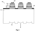
- Fig. 2 shows a principal sketch of a second VCSEL device 100 with guiding structure 132, which does not fall under the scope of the invention.
- the second VCSEL device 100 comprises an array of bottom emitting VCSELs which are arranged on a common substrate 110.
- Each VCSEL of the VCSEL array comprises a similar layer arrangement as described with respect to Fig. 1 .
- Each VCSEL of the VCSEL array is coupled with a lens structure 112 etched in a second side of the substrate 110 opposing the first side of the substrate 110.
- the lens structure 112 is arranged to focus the laser light emitted via the second side of the substrate 110 (indicated by the arrow).
- the lens structure 112 further provides optical feedback due to the differences in refractive index (GaAs ⁇ 3.4 and air 1).
- the lens structure 112 is therefore a part of the optical resonator and defines an extended optical cavity.
- Each VCSEL of the VCSEL array is therefore a Vertical Extended Cavity Surface Emitting Laser (VECSEL).
- VECSEL Vertical Extended Cavity Surface Emitting Laser
- a further difference with respect to the VCSEL device 100 shown in Fig. 1 is that the guiding structure 132 is not integrated in the second DBR 130.
- the guiding structure 132 comprises a structured second electrode.
- the structured second electrode provides local induction of electrical current in order to electrically pump separate relative intensity maxima such that there are a multitude of light emitting areas.
- the metal of the second electrode contributes to the reflectivity of the p-DBR and structures it laterally and therefore supports guiding in this respect to.
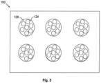
- Fig. 3 shows a principal sketch of a top view of a third VCSEL device 100 across the active layer 120, which does not fall under the scope of the invention.
- the cross-section shows an array of six bottom emitting VCSELs across the active layer.
- the general configuration of each VCSEL is similar as discussed with respect to Fig. 1 .
- the second electrical contact 135 fully covers the second DBR 130 (see also Fig 4 ).
- the second electrical contact 135 contributes to the reflectivity of the second reflecting structure comprising the second DBR.
- the second electrical contact is arranged to provide a lateral variation of the reflectivity such that the resonance conditions vary laterally across the optical resonator in order to provide separate optical modes with distinct intensity profile such that there are seven light emitting areas 124 within the active area 128 of the respective active layer 120.
- Each VCSEL may optionally comprise a structured current distribution layer (not shown) supporting optical guiding by inducing the current at positions where the resonance conditions of the optical resonator enables emission of laser light.
- the cavity gain can be modified laterally by a different reflectivity of the mirrors, in this case the second DBR 130 (p-DBR) as its surface is easy accessible to processing.
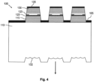
- Fig. 4 shows a principal sketch of a fourth VCSEL device 100 with guiding structure 132, which does not fall under the scope of the invention.
- the arrangement is very similar as discussed with respect to Fig. 2 .
- the second electrode 135 of the VCSELs of the VCSEL array fully covers the second DBR 130.
- the second side of the substrate 110 is in contrast to the embodiment discussed with respect to Fig. 2 arranged such that laterally varying optical feedback is provided across each active area.
- the second side of the substrate 110 is etched forming guiding structure 132.
- the localized external feedback of the guiding structure 132 across the respective active area enforces local (relative) intensity maxima of the intensity distribution in the active layer 120.
- a structured glass plate may be provided in order to enable such local optical feedback.
- a stable cavity relies on a thermal lens developing in the material. Because of symmetry and the major influence of heat flow to the outside of the mesa of the respective VCSEL such thermal lens will most likely cover the whole bottom emitter and not show the desirable sub-structure. Therefore it can be advantageous to use a guiding structure 132 with many small curved mirrors as shown in Fig. 4 instead of a simple flat surface with modulated reflectivity.
- Another embodiment would be small micro-lenses and a flat (common) mirror forming the array of stable cavities inside the large electrically-pumped region of each VCSEL of the VCSEL array.
- Fig. 5 shows a principal sketch of a cross-section of a fifth VCSEL device 100, which device does not fall under the scope of the invention.
- the fifth VCSEL device 100 is a VCSEL emitting laser light away from the substrate 110 (top emitter, laser emission indicated by the arrow).
- a first electrical contact 105 is provided on the second side of the substrate 110 .
- a first DBR 115 provided comprising 40 pairs of layers with a first and a second refractive index.
- the pairs of layers of the first DBR 115 comprise AlGaAs/GaAs layers.
- the thickness of the layers is adapted to the emission wavelength of the VCSEL device 100 in order to provide the requested reflectivity of more than 99.9%.
- the active layer 120 On top of the first DBR 115 is an active layer 120 provided.
- the active layer 120 comprises a quantum well structure for light generation.
- An n-current injection layer (not shown) may be arranged between the first DBR 115 and the active layer 120.
- a distributed HPT 125 is provided on top of the active layer 120.
- a current spreading layer 127 is arranged on top of the distributed HPT 125.
- a second DBR 130 is provided on top of the current spreading layer 127.
- the second DBR 130 is a dielectric DBR comprising pairs of non-conducting dielectric layers with different refractive indices as, for example, NbzOs, TiO 2 , TaO 2 , Si 3 N 4 and SiO 2 layers. The number of pair of layers depends on the materials and the intended reflectivity.
- the thickness of the pair of layers is adapted to the emission wavelength of the VCSEL device 100 in order to provide the requested reflectivity of around 97 %.
- a ring shaped second electrical contact 135 is arranged around the second dielectric DBR 130 above the current spreading layer.
- the VCSEL device 100 emits laser light in the direction of the arrow via the second dielectric DBR 130.
- the guiding structure 132 comprises a structured SiO 2 layer.
- the structured SiO 2 layer is embedded between the current spreading layer 127 and the second DBR 130.
- the SiO 2 layer is deposited on top of the current spreading layer 127 and subsequently etched to provide a lateral variation of optical feedback.
- the dielectric layers of the second DBR 130 are subsequently deposited on top of the structured SiO 2 layer and the current spreading layer 127 where the current spreading layer 127 was exposed by etching the SiO 2 layer.
- the structured SiO 2 layer locally increases the effective optical length and therefore the resonance condition of the optical resonator such that lasing is only enabled at the positions of remainders of the structured SiO 2 layer.
- Fig. 6 shows a cross-section of an optical sensor 300 according to a preferred embodiment.
- the optical sensor 300 comprises a VCSEL device 100 as described above, a transmission window 310 and a driving circuit 320 for electrically driving the VCSEL device 100.
- the driving circuit 320 is electrically connected to the VCSEL device 100 to supply electrical power to the VCSEL device 100 in a defined way.
- the driving circuit 320 comprises a memory device for storing data and instructions to operate the driving circuit 320 and a processing unit for executing data and instructions to operate the driving circuit 320.
- the optical sensor 300 further comprises a photo detector 350 and an evaluator 360.
- the photo detector 350 is in this case a photo diode but may be any preferably semiconductor device which can be used to detect laser light emitted by the VCSEL device 100.
- the photo detector 350 should be as sensitive as possible for the photons emitted by the VCSEL device 100 and should have a fast measurement time.
- a preferred technology are e.g. avalanche photodiodes or even more so called SPADs (single photon avalanche diodes) as well as arrays of the same.
- the evaluator 360 comprises at least one memory device like a memory chip and at least one processing device like a micro-processor.
- a small part of the emitted laser light 315 may be reflected at the transmission window 310 and used as control signal 319.
- the control signal 319 is received by means of the photo-detector 350 much earlier than the reflected laser light 317.
- the evaluator 360 is therefore able to differentiate between reception of control signal 319 and reflected laser light 317.
- the signal strength of the received control signal 319 is compared by means of the evaluator 360 with a reference signal strength stored in the memory device of the evaluator 360.
- the evaluator 360 sends a power reduction signal to the driving circuit 320 as soon as the signal strength of the received control signal 319 exceeds a threshold value which is based on the reference signal strength in order to guarantee eye safety of the optical sensor 300.
- the time between reception of control signal 319 and reflected laser light 317 may be rather short. It may thus be favorable to use a separate control signal 319 independent from the emitted laser light 315.
- the separate control signal 319 may be a very short laser pulse emitted between two laser pulses of the emitted laser light 315.
- the feedback structure may, for example, be a small piece of the surface of the transmission window 310 which is inclined with respect to the rest of the surface of the transmission window 310. Position and inclination angle are chosen such that the control signal 319 is directed to the photo-detector 350.
- Fig. 7 shows a principal sketch of a mobile communication device 380 comprising an optical sensor 300 similar as described with respect to Fig. 6 .
- the optical sensor 300 can, for example, be used in combination with a software application running on the mobile communication device 380.
- the software application may use the optical sensor 300 for sensing applications.
- Such sensing applications may be time of flight measurements for distance detection, camera autofocus, 3-D imaging of a scene or a gesture based user interface.
- Fig. 8 shows a principal sketch of a process flow of a method of fabricating a VCSEL device 100.
- a GaAs substrate 110 is provided in step 410.
- a first DBR 115 is provided on a first side of the substrate 110 in step 420 and an active layer 120 is provided in subsequent step 430 on top of the first DBR 115.
- a second DBR 130 provided in step 440 on top of the active layer 120.
- a first electrical contact 105 is provided in step 450. The first electrical contact 105 is attached to a second side of the substrate 110.
- a second electrical contact 135 is provided for electrically pumping the VCSEL device together with the first electrical contact 105 in step 460.
- a guiding structure 132 is provided step 470.
- Further approaches to implement the guiding structure 132 may be: 1.
- large diameter bottom emitter localized regions are defined by oxidation of more than one layer. While the large diameter bottom emitter is created by mesa etching and oxidation from the outside of the mesa, for the local separation an oxidation can take place through small holes etched into the surface. This allows a narrow spacing of localized regions inside the large bottom emitter providing an optically almost continuous large emitter.
- Non-perfect electrical isolation by the oxidation is tolerable as the optical separation with oxidized aluminum is very strong because of the large step in refractive index. Non-perfect electrical isolation therefore may reduce efficiency (as current is injected in non lasing regions) but the relative intensity maxima stay separated.
- the whole structure can have one continuous metal electrode connected to the electrical driver.
Landscapes
- Physics & Mathematics (AREA)
- Condensed Matter Physics & Semiconductors (AREA)
- General Physics & Mathematics (AREA)
- Electromagnetism (AREA)
- Optics & Photonics (AREA)
- Semiconductor Lasers (AREA)
Claims (9)
- Dispositif laser à cavité verticale émettant par la surface (100),le dispositif laser à cavité verticale émettant par la surface (100) comprend un premier contact électrique (105), un substrat (110), un second contact électrique (135) et un résonateur optique,le résonateur optique est agencé sur un premier côté du substrat (110),le résonateur optique comprend une première structure réfléchissante comprenant un premier réflecteur de Bragg distribué (115), une seconde structure réfléchissante comprenant un second réflecteur de Bragg distribué (130), une couche active (120) agencée entre la première structure réfléchissante et la seconde structure réfléchissante et une structure de guidage (132),dans lequel la structure de guidage (132) est agencée au sein d'un empilement de couches du premier réflecteur de Bragg distribué (115) ou du second réflecteur de Bragg distribué (130),dans lequel la structure de guidage (132) est configurée pour fournir une variation latérale d'une longueur optique efficace de la première structure réfléchissante ou de la seconde structure réfléchissante parallèle à la couche active (120), dans lequel la structure de guidage (132) est configurée pour définir- un premier maximum d'intensité relative d'une distribution d'intensité au sein de la couche active (120) au niveau d'une première position latérale du résonateur optique de telle sorte qu'une première zone électroluminescente (124) est fournie, et- au moins un second maximum d'intensité relative de la distribution d'intensité au sein de la couche active (120) au niveau d'une seconde position latérale du résonateur optique de telle sorte qu'une seconde zone électroluminescente (124) est fournie,dans lequel la structure de guidage (132) est en outre configurée pour réduire une intensité de la distribution d'intensité entre les au moins deux zones électroluminescentes (124) pendant le fonctionnement du dispositif laser à cavité verticale émettant par la surface (100), etcaractérisé en ce que la structure de guidage (132) comprend des régions oxydées de plus d'une couche du premier réflecteur de Bragg distribué (115) ou du second réflecteur de Bragg distribué (130), de sorte que la structure de guidage est agencée au sein de l'empilement de couches du premier réflecteur de Bragg distribué ou du second réflecteur de Bragg distribué dans une direction verticale du dispositif laser à cavité verticale émettant par la surface, etdans lequel les régions oxydées sont agencées pour réduire l'intensité entre les zones électroluminescentes (124), dans lequel l'intensité réduite entre les zones électroluminescentes est produite en fournissant une variation latérale de la condition de résonance à travers la couche active (120).
- Dispositif laser à cavité verticale émettant par la surface (100) selon l'une quelconque des revendications précédentes, dans lequel la structure de guidage (132) est agencée au sein du résonateur optique et totalement enfermée par celui-ci.
- Dispositif laser à cavité verticale émettant par la surface (100) selon l'une quelconque des revendications précédentes, dans lequel la structure de guidage (132) comprend en outre une variation latérale d'une réflectivité du premier contact électrique (105) ou du second contact électrique (130).
- Dispositif laser à cavité verticale émettant par la surface (100) selon l'une quelconque des revendications précédentes, dans lequel le résonateur optique comprend un phototransistor bipolaire à hétérojonction distribué (125), le phototransistor bipolaire à hétérojonction distribué (125) comprend une couche collectrice (125a), une couche sensible à la lumière (125c), une couche de base (125e) et une couche émettrice (125f), dans lequel le phototransistor bipolaire à hétérojonction distribué (125) est agencé de telle sorte qu'il existe un couplage optique entre la couche active (120) et le phototransistor bipolaire à hétérojonction distribué (125) pour fournir un confinement de porteuse active au moyen du phototransistor bipolaire à hétérojonction distribué (125) ; en particulier dans lequel la structure de guidage (132) est agencée en dehors d'un flux de courant qui peut être fourni au moyen du premier contact électrique (105) et du second contact électrique (135) pendant le fonctionnement du dispositif laser à cavité verticale émettant par la surface (100).
- Dispositif laser à cavité verticale émettant par la surface (100) selon l'une quelconque des revendications précédentes, dans lequel la structure de guidage (132) est configurée pour fournir à travers la section transversale latérale des régions de résonateur optique une longueur optique efficace permettant un fonctionnement de laser résonnant interrompu par des régions avec une longueur optique efficace différente inhibant le fonctionnement du laser.
- Dispositif laser à cavité verticale émettant par la surface (100) selon l'une quelconque des revendications précédentes, dans lequel la structure de guidage (132) est configurée pour fournir un confinement de courant local au niveau des zones électroluminescentes (124).
- Capteur optique (300) comprenant le dispositif laser à cavité verticale émettant par la surface (100) selon l'une quelconque des revendications précédentes.
- Dispositif de communication mobile (380) comprenant au moins un capteur optique (300) selon la revendication 7.
- Procédé de fabrication d'un dispositif laser à cavité verticale émettant par la surface, le procédé comprenant les étapes de :fourniture d'un premier contact électrique (105),fourniture d'un substrat (110),fourniture d'un premier réflecteur de Bragg distribué (115),fourniture d'une couche active (120),fourniture d'un second réflecteur de Bragg distribué (130),fourniture d'un second contact électrique (135),fourniture d'une structure de guidage (132) qui est agencée au sein d'un empilement de couches du premier réflecteur de Bragg distribué (115) ou du second réflecteur de Bragg distribué (130) et qui est configurée pour fournir une variation latérale d'une longueur optique efficace de la première structure réfléchissante ou de la seconde structure réfléchissante parallèle à la couche active (120), dans lequel la structure de guidage est configurée pour définir- un premier maximum d'intensité relative d'une distribution d'intensité au sein de la couche active (120) au niveau d'une première position latérale du résonateur optique de telle sorte qu'une première zone électroluminescente (124) est fournie, et- au moins un second maximum d'intensité relative de la distribution d'intensité au sein de la couche active (120) au niveau d'une seconde position latérale du résonateur optique de telle sorte qu'une seconde zone électroluminescente (124) est fournie,- dans lequel la structure de guidage (132) est en outre configurée pour réduire une intensité de la distribution d'intensité entre les au moins deux zones électroluminescentes (124) pendant le fonctionnement du dispositif laser à cavité verticale émettant par la surface (100), etcaractérisé en ce que la structure de guidage (132) comprend des régions oxydées de plus d'une couche du premier réflecteur de Bragg distribué (115) ou du second réflecteur de Bragg distribué (130), de sorte que la structure de guidage est agencée au sein de l'empilement de couches du premier réflecteur de Bragg distribué ou du second réflecteur de Bragg distribué dans une direction verticale du dispositif laser à cavité verticale émettant par la surface, etdans lequel les régions oxydées sont agencées pour réduire l'intensité entre les zones électroluminescentes (124), dans lequel l'intensité réduite entre les zones électroluminescentes est produite en fournissant une variation latérale de la condition de résonance à travers la couche active (120).
Applications Claiming Priority (3)
| Application Number | Priority Date | Filing Date | Title |
|---|---|---|---|
| EP17206157.4A EP3496216A1 (fr) | 2017-12-08 | 2017-12-08 | Laser à cavité verticale émettant en surface segmentée |
| PCT/EP2018/083833 WO2019110744A1 (fr) | 2017-12-08 | 2018-12-06 | Laser à cavité verticale émettant par la surface segmenté |
| EP18811309.6A EP3721513A1 (fr) | 2017-12-08 | 2018-12-06 | Laser à cavité verticale émettant par la surface segmenté |
Related Parent Applications (2)
| Application Number | Title | Priority Date | Filing Date |
|---|---|---|---|
| EP18811309.6A Division EP3721513A1 (fr) | 2017-12-08 | 2018-12-06 | Laser à cavité verticale émettant par la surface segmenté |
| EP18811309.6A Division-Into EP3721513A1 (fr) | 2017-12-08 | 2018-12-06 | Laser à cavité verticale émettant par la surface segmenté |
Publications (2)
| Publication Number | Publication Date |
|---|---|
| EP3761464A1 EP3761464A1 (fr) | 2021-01-06 |
| EP3761464B1 true EP3761464B1 (fr) | 2024-08-14 |
Family
ID=60629570
Family Applications (3)
| Application Number | Title | Priority Date | Filing Date |
|---|---|---|---|
| EP17206157.4A Withdrawn EP3496216A1 (fr) | 2017-12-08 | 2017-12-08 | Laser à cavité verticale émettant en surface segmentée |
| EP18811309.6A Pending EP3721513A1 (fr) | 2017-12-08 | 2018-12-06 | Laser à cavité verticale émettant par la surface segmenté |
| EP20184734.0A Active EP3761464B1 (fr) | 2017-12-08 | 2018-12-06 | Laser à cavité verticale émettant en surface segmentée |
Family Applications Before (2)
| Application Number | Title | Priority Date | Filing Date |
|---|---|---|---|
| EP17206157.4A Withdrawn EP3496216A1 (fr) | 2017-12-08 | 2017-12-08 | Laser à cavité verticale émettant en surface segmentée |
| EP18811309.6A Pending EP3721513A1 (fr) | 2017-12-08 | 2018-12-06 | Laser à cavité verticale émettant par la surface segmenté |
Country Status (7)
| Country | Link |
|---|---|
| US (1) | US11563306B2 (fr) |
| EP (3) | EP3496216A1 (fr) |
| CN (1) | CN111699598B (fr) |
| DE (1) | DE102018131615A1 (fr) |
| FR (1) | FR3076960A1 (fr) |
| GB (1) | GB2570565A (fr) |
| WO (1) | WO2019110744A1 (fr) |
Families Citing this family (17)
| Publication number | Priority date | Publication date | Assignee | Title |
|---|---|---|---|---|
| JP7190865B2 (ja) * | 2018-10-18 | 2022-12-16 | スタンレー電気株式会社 | 垂直共振器型発光素子 |
| JP7166871B2 (ja) | 2018-10-18 | 2022-11-08 | スタンレー電気株式会社 | 垂直共振器型発光素子 |
| DE102019216710A1 (de) * | 2019-10-30 | 2021-05-06 | OSRAM Opto Semiconductors Gesellschaft mit beschränkter Haftung | Optoelektronisches halbleiterbauelement, anordnung von optoelektronischen halbleiterbauelementen, optoelektronische vorrichtung und verfahren zur herstellung eines optoelektronischen halbleiterbauelementes |
| EP4073585A1 (fr) * | 2019-12-10 | 2022-10-19 | TRUMPF Photonic Components GmbH | Procédé de formation lithographique d'une structure optique dans un substrat semi-conducteur |
| US12548979B2 (en) | 2020-02-24 | 2026-02-10 | Shenzhen Raysees AI Technology Co., Ltd. | VCSEL array with non-isolated emitters |
| EP3982167A1 (fr) * | 2020-10-06 | 2022-04-13 | TRUMPF Photonic Components GmbH | Lentille de diffuseur, source de lumière, procédé de fabrication d'une source de lumière et procédé d'éclairage d'une scène |
| CN115207773A (zh) * | 2021-04-09 | 2022-10-18 | 浙江睿熙科技有限公司 | 在晶圆级别集成的vcsel器件和vcsel器件的制备方法 |
| US12362541B2 (en) * | 2021-04-30 | 2025-07-15 | Lumentum Operations Llc | Methods for incorporating a control structure within a vertical cavity surface emitting laser device cavity |
| US12542425B2 (en) | 2021-08-16 | 2026-02-03 | Shenzhen Raysees Ai Technology Co. Ltd. | VCSEL array with different emitter structures |
| DE102021122386A1 (de) | 2021-08-30 | 2023-03-02 | Trumpf Photonic Components Gmbh | Vertikaler oberflächenemittierender Hohlraumlaser (VCSEL), Lasersensor und Verfahren zur Herstellung eines VCSEL |
| US12188998B2 (en) | 2022-11-08 | 2025-01-07 | Honeywell International Inc. | Integrated photonics magnetometer based on a nonlinear diamond-containing resonator |
| JP2024081832A (ja) * | 2022-12-07 | 2024-06-19 | ソニーセミコンダクタソリューションズ株式会社 | 光学装置及び光学装置の製造方法 |
| CN116826507A (zh) * | 2023-04-14 | 2023-09-29 | 苏州立琻半导体有限公司 | 光源模组 |
| DE102023133477A1 (de) * | 2023-11-30 | 2025-06-05 | Trumpf Photonic Components Gmbh | VCSEL und Verfahren zum Herstellen eines VCSEL |
| US12493087B2 (en) | 2023-12-20 | 2025-12-09 | Honeywell International Inc. | Vertical cavity surface-emitting laser threshold magnetometer |
| US12517191B2 (en) | 2024-02-29 | 2026-01-06 | Honeywell International Inc. | Chip scale magnetometer |
| WO2026004394A1 (fr) * | 2024-06-25 | 2026-01-02 | ソニーグループ株式会社 | Dispositif électroluminescent |
Citations (3)
| Publication number | Priority date | Publication date | Assignee | Title |
|---|---|---|---|---|
| US6061381A (en) * | 1995-09-29 | 2000-05-09 | British Telecommunications Public Limited Company | Optically resonant structure |
| WO2008043526A1 (fr) * | 2006-10-10 | 2008-04-17 | Firecomms Limited | Dispositifs optiques d'émission en surface |
| US20170033535A1 (en) * | 2015-07-30 | 2017-02-02 | Optipulse Inc. | Rigid High Power and High Speed Lasing Grid Structures |
Family Cites Families (16)
| Publication number | Priority date | Publication date | Assignee | Title |
|---|---|---|---|---|
| US6751245B1 (en) * | 1999-06-02 | 2004-06-15 | Optical Communication Products, Inc. | Single mode vertical cavity surface emitting laser |
| AU2000258686A1 (en) * | 1999-06-02 | 2001-12-17 | Cielo Communications, Inc. | Single mode vertical cavity surface emitting laser |
| US6507595B1 (en) * | 1999-11-22 | 2003-01-14 | Avalon Photonics | Vertical-cavity surface-emitting laser comprised of single laser elements arranged on a common substrate |
| US20030031218A1 (en) * | 2001-08-13 | 2003-02-13 | Jang-Hun Yeh | VCSEL structure and method of making same |
| US7257141B2 (en) * | 2003-07-23 | 2007-08-14 | Palo Alto Research Center Incorporated | Phase array oxide-confined VCSELs |
| WO2006056208A2 (fr) * | 2004-11-29 | 2006-06-01 | Alight Technologies A/S | Vcsel a cristal photonique monomode |
| KR101253396B1 (ko) * | 2008-02-12 | 2013-04-15 | 가부시키가이샤 리코 | 면 발광 레이저 소자, 면 발광 레이저 어레이, 광 주사 장치, 및 화상 형성 장치 |
| US8355417B2 (en) * | 2008-10-14 | 2013-01-15 | Koninklijke Philips Electronics N.V. | Vertical cavity surface emitting laser with improved mode-selectivity |
| US9112332B2 (en) * | 2012-06-14 | 2015-08-18 | Palo Alto Research Center Incorporated | Electron beam pumped vertical cavity surface emitting laser |
| JP6102525B2 (ja) | 2012-07-23 | 2017-03-29 | 株式会社リコー | 面発光レーザ素子及び原子発振器 |
| WO2014080770A1 (fr) * | 2012-11-21 | 2014-05-30 | 古河電気工業株式会社 | Dispositif laser émettant par la surface, module optique et méthode d'excitation d'élément laser émettant par la surface |
| US20150311673A1 (en) * | 2014-04-29 | 2015-10-29 | Princeton Optronics Inc. | Polarization Control in High Peak Power, High Brightness VCSEL |
| US9882355B2 (en) * | 2014-09-25 | 2018-01-30 | Koninklijke Philips N.V. | Vertical cavity surface emitting laser |
| BR112017021395A2 (pt) * | 2015-04-10 | 2018-07-03 | Koninklijke Philips Nv | dispositivo de laser, módulo de laser, sensor óptico, dispositivo de comunicação móvel, e método de fabricação de um dispositivo de laser |
| US9780532B1 (en) * | 2016-11-21 | 2017-10-03 | Palo Alto Research Center Incorporated | Vertical external cavity surface emitting laser utilizing an external micromirror array |
| US9843160B1 (en) * | 2016-12-29 | 2017-12-12 | X Development Llc | Integrated digital laser |
-
2017
- 2017-12-08 EP EP17206157.4A patent/EP3496216A1/fr not_active Withdrawn
-
2018
- 2018-12-06 EP EP18811309.6A patent/EP3721513A1/fr active Pending
- 2018-12-06 EP EP20184734.0A patent/EP3761464B1/fr active Active
- 2018-12-06 CN CN201880087329.2A patent/CN111699598B/zh active Active
- 2018-12-06 WO PCT/EP2018/083833 patent/WO2019110744A1/fr not_active Ceased
- 2018-12-07 FR FR1872510A patent/FR3076960A1/fr not_active Ceased
- 2018-12-07 GB GB1819993.5A patent/GB2570565A/en not_active Withdrawn
- 2018-12-10 DE DE102018131615.1A patent/DE102018131615A1/de not_active Withdrawn
-
2020
- 2020-06-08 US US16/895,017 patent/US11563306B2/en active Active
Patent Citations (3)
| Publication number | Priority date | Publication date | Assignee | Title |
|---|---|---|---|---|
| US6061381A (en) * | 1995-09-29 | 2000-05-09 | British Telecommunications Public Limited Company | Optically resonant structure |
| WO2008043526A1 (fr) * | 2006-10-10 | 2008-04-17 | Firecomms Limited | Dispositifs optiques d'émission en surface |
| US20170033535A1 (en) * | 2015-07-30 | 2017-02-02 | Optipulse Inc. | Rigid High Power and High Speed Lasing Grid Structures |
Also Published As
| Publication number | Publication date |
|---|---|
| DE102018131615A1 (de) | 2019-06-13 |
| EP3761464A1 (fr) | 2021-01-06 |
| US20200303902A1 (en) | 2020-09-24 |
| US11563306B2 (en) | 2023-01-24 |
| GB201819993D0 (en) | 2019-01-23 |
| GB2570565A (en) | 2019-07-31 |
| EP3721513A1 (fr) | 2020-10-14 |
| CN111699598B (zh) | 2023-11-07 |
| CN111699598A (zh) | 2020-09-22 |
| WO2019110744A1 (fr) | 2019-06-13 |
| EP3496216A1 (fr) | 2019-06-12 |
| FR3076960A1 (fr) | 2019-07-19 |
Similar Documents
| Publication | Publication Date | Title |
|---|---|---|
| EP3761464B1 (fr) | Laser à cavité verticale émettant en surface segmentée | |
| CN112470352B (zh) | 具有集成的隧道结的垂直腔面发射激光器装置 | |
| US11411374B2 (en) | Vertical cavity surface emitting laser (VCSEL) with improved gain-switching behavior | |
| US12034272B2 (en) | Vertical cavity surface emitting laser device with integrated photodiode | |
| CN107466431B (zh) | 用于光学传感应用的安全激光设备 | |
| US11469572B2 (en) | Vertical cavity surface emitting laser | |
| KR102630495B1 (ko) | 모놀리식 집적 포토다이오드를 갖는 수직 공동 면 발광 레이저 장치 | |
| JP7840827B2 (ja) | 半導体発光素子、発光装置、及び測距装置 | |
| US10535976B1 (en) | Optical device and system having thermal buffers |
Legal Events
| Date | Code | Title | Description |
|---|---|---|---|
| PUAI | Public reference made under article 153(3) epc to a published international application that has entered the european phase |
Free format text: ORIGINAL CODE: 0009012 |
|
| STAA | Information on the status of an ep patent application or granted ep patent |
Free format text: STATUS: REQUEST FOR EXAMINATION WAS MADE |
|
| 17P | Request for examination filed |
Effective date: 20200708 |
|
| AC | Divisional application: reference to earlier application |
Ref document number: 3721513 Country of ref document: EP Kind code of ref document: P |
|
| AK | Designated contracting states |
Kind code of ref document: A1 Designated state(s): AL AT BE BG CH CY CZ DE DK EE ES FI FR GB GR HR HU IE IS IT LI LT LU LV MC MK MT NL NO PL PT RO RS SE SI SK SM TR |
|
| AX | Request for extension of the european patent |
Extension state: BA ME |
|
| STAA | Information on the status of an ep patent application or granted ep patent |
Free format text: STATUS: EXAMINATION IS IN PROGRESS |
|
| 17Q | First examination report despatched |
Effective date: 20220302 |
|
| GRAP | Despatch of communication of intention to grant a patent |
Free format text: ORIGINAL CODE: EPIDOSNIGR1 |
|
| STAA | Information on the status of an ep patent application or granted ep patent |
Free format text: STATUS: GRANT OF PATENT IS INTENDED |
|
| INTG | Intention to grant announced |
Effective date: 20240307 |
|
| GRAS | Grant fee paid |
Free format text: ORIGINAL CODE: EPIDOSNIGR3 |
|
| GRAA | (expected) grant |
Free format text: ORIGINAL CODE: 0009210 |
|
| STAA | Information on the status of an ep patent application or granted ep patent |
Free format text: STATUS: THE PATENT HAS BEEN GRANTED |
|
| AC | Divisional application: reference to earlier application |
Ref document number: 3721513 Country of ref document: EP Kind code of ref document: P |
|
| AK | Designated contracting states |
Kind code of ref document: B1 Designated state(s): AL AT BE BG CH CY CZ DE DK EE ES FI FR GB GR HR HU IE IS IT LI LT LU LV MC MK MT NL NO PL PT RO RS SE SI SK SM TR |
|
| REG | Reference to a national code |
Ref country code: GB Ref legal event code: FG4D |
|
| REG | Reference to a national code |
Ref country code: CH Ref legal event code: EP |
|
| REG | Reference to a national code |
Ref country code: DE Ref legal event code: R096 Ref document number: 602018073253 Country of ref document: DE |
|
| REG | Reference to a national code |
Ref country code: IE Ref legal event code: FG4D |
|
| REG | Reference to a national code |
Ref country code: LT Ref legal event code: MG9D |
|
| REG | Reference to a national code |
Ref country code: NL Ref legal event code: MP Effective date: 20240814 |
|
| PG25 | Lapsed in a contracting state [announced via postgrant information from national office to epo] |
Ref country code: NO Free format text: LAPSE BECAUSE OF FAILURE TO SUBMIT A TRANSLATION OF THE DESCRIPTION OR TO PAY THE FEE WITHIN THE PRESCRIBED TIME-LIMIT Effective date: 20241114 |
|
| REG | Reference to a national code |
Ref country code: AT Ref legal event code: MK05 Ref document number: 1714177 Country of ref document: AT Kind code of ref document: T Effective date: 20240814 |
|
| PG25 | Lapsed in a contracting state [announced via postgrant information from national office to epo] |
Ref country code: FI Free format text: LAPSE BECAUSE OF FAILURE TO SUBMIT A TRANSLATION OF THE DESCRIPTION OR TO PAY THE FEE WITHIN THE PRESCRIBED TIME-LIMIT Effective date: 20240814 Ref country code: NL Free format text: LAPSE BECAUSE OF FAILURE TO SUBMIT A TRANSLATION OF THE DESCRIPTION OR TO PAY THE FEE WITHIN THE PRESCRIBED TIME-LIMIT Effective date: 20240814 Ref country code: PL Free format text: LAPSE BECAUSE OF FAILURE TO SUBMIT A TRANSLATION OF THE DESCRIPTION OR TO PAY THE FEE WITHIN THE PRESCRIBED TIME-LIMIT Effective date: 20240814 Ref country code: GR Free format text: LAPSE BECAUSE OF FAILURE TO SUBMIT A TRANSLATION OF THE DESCRIPTION OR TO PAY THE FEE WITHIN THE PRESCRIBED TIME-LIMIT Effective date: 20241115 Ref country code: PT Free format text: LAPSE BECAUSE OF FAILURE TO SUBMIT A TRANSLATION OF THE DESCRIPTION OR TO PAY THE FEE WITHIN THE PRESCRIBED TIME-LIMIT Effective date: 20241216 |
|
| PG25 | Lapsed in a contracting state [announced via postgrant information from national office to epo] |
Ref country code: BG Free format text: LAPSE BECAUSE OF FAILURE TO SUBMIT A TRANSLATION OF THE DESCRIPTION OR TO PAY THE FEE WITHIN THE PRESCRIBED TIME-LIMIT Effective date: 20240814 |
|
| PG25 | Lapsed in a contracting state [announced via postgrant information from national office to epo] |
Ref country code: LV Free format text: LAPSE BECAUSE OF FAILURE TO SUBMIT A TRANSLATION OF THE DESCRIPTION OR TO PAY THE FEE WITHIN THE PRESCRIBED TIME-LIMIT Effective date: 20240814 |
|
| PG25 | Lapsed in a contracting state [announced via postgrant information from national office to epo] |
Ref country code: AT Free format text: LAPSE BECAUSE OF FAILURE TO SUBMIT A TRANSLATION OF THE DESCRIPTION OR TO PAY THE FEE WITHIN THE PRESCRIBED TIME-LIMIT Effective date: 20240814 Ref country code: IS Free format text: LAPSE BECAUSE OF FAILURE TO SUBMIT A TRANSLATION OF THE DESCRIPTION OR TO PAY THE FEE WITHIN THE PRESCRIBED TIME-LIMIT Effective date: 20241214 |
|
| PG25 | Lapsed in a contracting state [announced via postgrant information from national office to epo] |
Ref country code: HR Free format text: LAPSE BECAUSE OF FAILURE TO SUBMIT A TRANSLATION OF THE DESCRIPTION OR TO PAY THE FEE WITHIN THE PRESCRIBED TIME-LIMIT Effective date: 20240814 |
|
| PG25 | Lapsed in a contracting state [announced via postgrant information from national office to epo] |
Ref country code: RS Free format text: LAPSE BECAUSE OF FAILURE TO SUBMIT A TRANSLATION OF THE DESCRIPTION OR TO PAY THE FEE WITHIN THE PRESCRIBED TIME-LIMIT Effective date: 20241114 Ref country code: ES Free format text: LAPSE BECAUSE OF FAILURE TO SUBMIT A TRANSLATION OF THE DESCRIPTION OR TO PAY THE FEE WITHIN THE PRESCRIBED TIME-LIMIT Effective date: 20240814 |
|
| PG25 | Lapsed in a contracting state [announced via postgrant information from national office to epo] |
Ref country code: RS Free format text: LAPSE BECAUSE OF FAILURE TO SUBMIT A TRANSLATION OF THE DESCRIPTION OR TO PAY THE FEE WITHIN THE PRESCRIBED TIME-LIMIT Effective date: 20241114 Ref country code: PT Free format text: LAPSE BECAUSE OF FAILURE TO SUBMIT A TRANSLATION OF THE DESCRIPTION OR TO PAY THE FEE WITHIN THE PRESCRIBED TIME-LIMIT Effective date: 20241216 Ref country code: PL Free format text: LAPSE BECAUSE OF FAILURE TO SUBMIT A TRANSLATION OF THE DESCRIPTION OR TO PAY THE FEE WITHIN THE PRESCRIBED TIME-LIMIT Effective date: 20240814 Ref country code: NO Free format text: LAPSE BECAUSE OF FAILURE TO SUBMIT A TRANSLATION OF THE DESCRIPTION OR TO PAY THE FEE WITHIN THE PRESCRIBED TIME-LIMIT Effective date: 20241114 Ref country code: NL Free format text: LAPSE BECAUSE OF FAILURE TO SUBMIT A TRANSLATION OF THE DESCRIPTION OR TO PAY THE FEE WITHIN THE PRESCRIBED TIME-LIMIT Effective date: 20240814 Ref country code: LV Free format text: LAPSE BECAUSE OF FAILURE TO SUBMIT A TRANSLATION OF THE DESCRIPTION OR TO PAY THE FEE WITHIN THE PRESCRIBED TIME-LIMIT Effective date: 20240814 Ref country code: IS Free format text: LAPSE BECAUSE OF FAILURE TO SUBMIT A TRANSLATION OF THE DESCRIPTION OR TO PAY THE FEE WITHIN THE PRESCRIBED TIME-LIMIT Effective date: 20241214 Ref country code: HR Free format text: LAPSE BECAUSE OF FAILURE TO SUBMIT A TRANSLATION OF THE DESCRIPTION OR TO PAY THE FEE WITHIN THE PRESCRIBED TIME-LIMIT Effective date: 20240814 Ref country code: GR Free format text: LAPSE BECAUSE OF FAILURE TO SUBMIT A TRANSLATION OF THE DESCRIPTION OR TO PAY THE FEE WITHIN THE PRESCRIBED TIME-LIMIT Effective date: 20241115 Ref country code: FI Free format text: LAPSE BECAUSE OF FAILURE TO SUBMIT A TRANSLATION OF THE DESCRIPTION OR TO PAY THE FEE WITHIN THE PRESCRIBED TIME-LIMIT Effective date: 20240814 Ref country code: ES Free format text: LAPSE BECAUSE OF FAILURE TO SUBMIT A TRANSLATION OF THE DESCRIPTION OR TO PAY THE FEE WITHIN THE PRESCRIBED TIME-LIMIT Effective date: 20240814 Ref country code: BG Free format text: LAPSE BECAUSE OF FAILURE TO SUBMIT A TRANSLATION OF THE DESCRIPTION OR TO PAY THE FEE WITHIN THE PRESCRIBED TIME-LIMIT Effective date: 20240814 Ref country code: AT Free format text: LAPSE BECAUSE OF FAILURE TO SUBMIT A TRANSLATION OF THE DESCRIPTION OR TO PAY THE FEE WITHIN THE PRESCRIBED TIME-LIMIT Effective date: 20240814 |
|
| PG25 | Lapsed in a contracting state [announced via postgrant information from national office to epo] |
Ref country code: SM Free format text: LAPSE BECAUSE OF FAILURE TO SUBMIT A TRANSLATION OF THE DESCRIPTION OR TO PAY THE FEE WITHIN THE PRESCRIBED TIME-LIMIT Effective date: 20240814 Ref country code: RO Free format text: LAPSE BECAUSE OF FAILURE TO SUBMIT A TRANSLATION OF THE DESCRIPTION OR TO PAY THE FEE WITHIN THE PRESCRIBED TIME-LIMIT Effective date: 20240814 Ref country code: DK Free format text: LAPSE BECAUSE OF FAILURE TO SUBMIT A TRANSLATION OF THE DESCRIPTION OR TO PAY THE FEE WITHIN THE PRESCRIBED TIME-LIMIT Effective date: 20240814 |
|
| PG25 | Lapsed in a contracting state [announced via postgrant information from national office to epo] |
Ref country code: EE Free format text: LAPSE BECAUSE OF FAILURE TO SUBMIT A TRANSLATION OF THE DESCRIPTION OR TO PAY THE FEE WITHIN THE PRESCRIBED TIME-LIMIT Effective date: 20240814 |
|
| PG25 | Lapsed in a contracting state [announced via postgrant information from national office to epo] |
Ref country code: CZ Free format text: LAPSE BECAUSE OF FAILURE TO SUBMIT A TRANSLATION OF THE DESCRIPTION OR TO PAY THE FEE WITHIN THE PRESCRIBED TIME-LIMIT Effective date: 20240814 |
|
| PG25 | Lapsed in a contracting state [announced via postgrant information from national office to epo] |
Ref country code: SK Free format text: LAPSE BECAUSE OF FAILURE TO SUBMIT A TRANSLATION OF THE DESCRIPTION OR TO PAY THE FEE WITHIN THE PRESCRIBED TIME-LIMIT Effective date: 20240814 Ref country code: IT Free format text: LAPSE BECAUSE OF FAILURE TO SUBMIT A TRANSLATION OF THE DESCRIPTION OR TO PAY THE FEE WITHIN THE PRESCRIBED TIME-LIMIT Effective date: 20240814 |
|
| REG | Reference to a national code |
Ref country code: DE Ref legal event code: R097 Ref document number: 602018073253 Country of ref document: DE |
|
| PLBE | No opposition filed within time limit |
Free format text: ORIGINAL CODE: 0009261 |
|
| STAA | Information on the status of an ep patent application or granted ep patent |
Free format text: STATUS: NO OPPOSITION FILED WITHIN TIME LIMIT |
|
| PG25 | Lapsed in a contracting state [announced via postgrant information from national office to epo] |
Ref country code: MC Free format text: LAPSE BECAUSE OF FAILURE TO SUBMIT A TRANSLATION OF THE DESCRIPTION OR TO PAY THE FEE WITHIN THE PRESCRIBED TIME-LIMIT Effective date: 20240814 |
|
| 26N | No opposition filed |
Effective date: 20250515 |
|
| REG | Reference to a national code |
Ref country code: CH Ref legal event code: PL |
|
| PG25 | Lapsed in a contracting state [announced via postgrant information from national office to epo] |
Ref country code: LU Free format text: LAPSE BECAUSE OF NON-PAYMENT OF DUE FEES Effective date: 20241206 |
|
| GBPC | Gb: european patent ceased through non-payment of renewal fee |
Effective date: 20241206 |
|
| PG25 | Lapsed in a contracting state [announced via postgrant information from national office to epo] |
Ref country code: SE Free format text: LAPSE BECAUSE OF FAILURE TO SUBMIT A TRANSLATION OF THE DESCRIPTION OR TO PAY THE FEE WITHIN THE PRESCRIBED TIME-LIMIT Effective date: 20240814 |
|
| REG | Reference to a national code |
Ref country code: BE Ref legal event code: MM Effective date: 20241231 |
|
| PG25 | Lapsed in a contracting state [announced via postgrant information from national office to epo] |
Ref country code: GB Free format text: LAPSE BECAUSE OF NON-PAYMENT OF DUE FEES Effective date: 20241206 Ref country code: BE Free format text: LAPSE BECAUSE OF NON-PAYMENT OF DUE FEES Effective date: 20241231 |
|
| PG25 | Lapsed in a contracting state [announced via postgrant information from national office to epo] |
Ref country code: FR Free format text: LAPSE BECAUSE OF NON-PAYMENT OF DUE FEES Effective date: 20241231 |
|
| PG25 | Lapsed in a contracting state [announced via postgrant information from national office to epo] |
Ref country code: CH Free format text: LAPSE BECAUSE OF NON-PAYMENT OF DUE FEES Effective date: 20241231 |
|
| PG25 | Lapsed in a contracting state [announced via postgrant information from national office to epo] |
Ref country code: IE Free format text: LAPSE BECAUSE OF NON-PAYMENT OF DUE FEES Effective date: 20241206 |
|
| PG25 | Lapsed in a contracting state [announced via postgrant information from national office to epo] |
Ref country code: CY Free format text: LAPSE BECAUSE OF FAILURE TO SUBMIT A TRANSLATION OF THE DESCRIPTION OR TO PAY THE FEE WITHIN THE PRESCRIBED TIME-LIMIT; INVALID AB INITIO Effective date: 20181206 |
|
| PGFP | Annual fee paid to national office [announced via postgrant information from national office to epo] |
Ref country code: DE Payment date: 20251229 Year of fee payment: 8 |