EP3761476A1 - Ladeschaltung und -verfahren für elektronische vorrichtung, vorrichtung und speichermedium - Google Patents
Ladeschaltung und -verfahren für elektronische vorrichtung, vorrichtung und speichermedium Download PDFInfo
- Publication number
- EP3761476A1 EP3761476A1 EP19916792.5A EP19916792A EP3761476A1 EP 3761476 A1 EP3761476 A1 EP 3761476A1 EP 19916792 A EP19916792 A EP 19916792A EP 3761476 A1 EP3761476 A1 EP 3761476A1
- Authority
- EP
- European Patent Office
- Prior art keywords
- charging
- charge pump
- switch component
- voltage
- switch
- Prior art date
- Legal status (The legal status is an assumption and is not a legal conclusion. Google has not performed a legal analysis and makes no representation as to the accuracy of the status listed.)
- Granted
Links
Images


Classifications
-
- H—ELECTRICITY
- H02—GENERATION; CONVERSION OR DISTRIBUTION OF ELECTRIC POWER
- H02M—APPARATUS FOR CONVERSION BETWEEN AC AND AC, BETWEEN AC AND DC, OR BETWEEN DC AND DC, AND FOR USE WITH MAINS OR SIMILAR POWER SUPPLY SYSTEMS; CONVERSION OF DC OR AC INPUT POWER INTO SURGE OUTPUT POWER; CONTROL OR REGULATION THEREOF
- H02M3/00—Conversion of DC power input into DC power output
- H02M3/02—Conversion of DC power input into DC power output without intermediate conversion into AC
- H02M3/04—Conversion of DC power input into DC power output without intermediate conversion into AC by static converters
- H02M3/06—Conversion of DC power input into DC power output without intermediate conversion into AC by static converters using resistors or capacitors, e.g. potential divider
- H02M3/07—Conversion of DC power input into DC power output without intermediate conversion into AC by static converters using resistors or capacitors, e.g. potential divider using capacitors charged and discharged alternately by semiconductor devices with control electrode, e.g. charge pumps
-
- H—ELECTRICITY
- H02—GENERATION; CONVERSION OR DISTRIBUTION OF ELECTRIC POWER
- H02J—ELECTRIC POWER NETWORKS; CIRCUIT ARRANGEMENTS OR SYSTEMS FOR SUPPLYING OR DISTRIBUTING ELECTRIC POWER; SYSTEMS FOR STORING ELECTRIC ENERGY
- H02J7/00—Circuit arrangements for charging or discharging batteries or for supplying loads from batteries
- H02J7/90—Regulation of charging or discharging current or voltage
-
- H—ELECTRICITY
- H02—GENERATION; CONVERSION OR DISTRIBUTION OF ELECTRIC POWER
- H02J—ELECTRIC POWER NETWORKS; CIRCUIT ARRANGEMENTS OR SYSTEMS FOR SUPPLYING OR DISTRIBUTING ELECTRIC POWER; SYSTEMS FOR STORING ELECTRIC ENERGY
- H02J2207/00—Details of circuit arrangements for charging or discharging batteries or supplying loads from batteries
- H02J2207/20—Charging or discharging characterised by the power electronics converter
Definitions
- This disclosure relates to electronic technology, including, but not limited to, a charging circuit for an electronic device, a charging method, an electronic device, and a storage medium.
- a charging circuit for an electronic device a charging method, an electronic device, and a storage medium are provided to solve at least one problem existing in the related art.
- a charging circuit for an electronic device includes a control module, a charge pump, and a battery assembly.
- the control module is configured to generate a first control signal upon detecting that a power adaptor connected is an adaptor for direct charging with high voltage.
- the charge pump is configured to, upon receiving the first control signal, directly apply a charging voltage to the battery assembly for direct charging, where the charging voltage is applied to the electronic device by the power adaptor.
- a charging method includes the following.
- a first control signal is generated upon detecting that a power adaptor connected is an adaptor for direct charging with high voltage.
- a charge pump of a charging circuit is controlled according to the first control signal to be switched on, to directly apply a charging voltage to a battery assembly for direct charging, where the charging voltage is applied to the electronic device by the power adaptor.
- an electronic device in a third aspect, includes a memory and a processor.
- the memory is configured to store computer programs which, when executed by the processor, are operable with the processor to perform the charging method described in the second aspect.
- a computer readable storage medium configured to store computer programs which, when executed by a processor, are operable with the processor to perform the charging method described in the second aspect.
- Implementations provide the charging circuit for an electronic device.
- the charging voltage applied to the electronic device by the power adaptor passes through the charge pump to be directly applied to the battery assembly for direct charging, which can decrease the number of devices required for the charging circuit, thereby improving charging efficiency.
- Implementations provide a charging circuit for an electronic device.
- the electronic device can be a mobile phone, a tablet computer, a desktop, a personal digital assistant (PDA), a global positioning system (GPS), a digital telephone, a video telephone, a television, a sensor device, etc.
- PDA personal digital assistant
- GPS global positioning system
- FIG. 1A is a schematic structural diagram of a charging circuit for an electronic device according to implementations.
- the charging circuit 10 includes a control module 101, a charge pump 102, and a battery assembly 103.
- the control module 101 is configured to generate a first control signal upon detecting that a power adaptor connected is an adaptor for direct charging with high voltage, or generate a second control signal upon detecting that the power adaptor is an adaptor for direct charging with low voltage.
- the first control signal is for controlling the charge pump 102 to be switched on in such a manner that a charging voltage is directly applied to the battery assembly 103 for direct charging, where the charging voltage is applied to the electronic device by the power adaptor.
- the second control signal is for controlling the charge pump 102 to perform boost conversion on the charging voltage and apply the charging voltage subjected to the boost conversion to the battery assembly 103 for charging.
- the power adaptor can be electrically coupled with the charge pump 102 via a charging interface (such as, for example, a Type-C interface, a universal serial bus (USB) interface, etc.) of the electronic device.
- a charging interface such as, for example, a Type-C interface, a universal serial bus (USB) interface, etc.
- the adaptor for direct charging with high voltage has a maximum output voltage that is higher than a voltage of the battery assembly (that is, a potential difference between a positive electrode and a negative electrode of the battery assembly).
- the adaptor for direct charging with low voltage has a maximum output voltage that is lower than the voltage of the battery assembly.
- the maximum output voltage of the adaptor for direct charging with low voltage is lower than that of the adaptor for direct charging with high voltage.
- the control module 101 can determine the type of the power adaptor as follows. The control module 101 determines that the power adaptor is the adaptor for direct charging with high voltage upon detecting that the charging voltage, which is applied to the electronic device by the power adaptor, is higher than a preset threshold voltage.
- the control module 101 determines that the power adaptor is the adaptor for direct charging with low voltage upon detecting that the charging voltage, which is applied to the electronic device by the power adaptor, is lower than or equal to the preset threshold voltage.
- the power adaptor can send directly a communication signal to the control module 101 to notify the control module 101 of the type of the power adaptor.
- the charge pump 102 is configured to operate as follows.
- the charge pump 102 is configured to, upon receiving the first control signal, directly apply the charging voltage to the battery assembly 103 for direct charging, where the charging voltage is applied to the electronic device by the power adaptor.
- the charge pump 102 is configured to perform, upon receiving the second control signal, boost conversion on the charging voltage and apply the charging voltage subjected to the boost conversion to the battery assembly 103 for charging.
- the battery assembly 103 includes at least one cell.
- the charge pump 102 upon receiving the first control signal, can directly switch on a line 1021 in which only a switch component(s) is provided, such that the charging voltage applied to the electronic device by the power adaptor 104 is directly applied to the battery assembly 103 for direct charging.
- a direct-charging path 1021 of the charge pump 102 will be switched on, and as such, the charge pump 102 will directly apply the charging voltage to the battery assembly for direct charging.
- the direct-charging path 1021 can be provided with only switch components, such that there is no other power consuming components.
- the charge pump when the battery assembly 103 is charged with the adaptor for direct charging with high voltage, the charge pump is in a circuit state which is referred to as a bypass mode.
- the charge pump 102 When the battery assembly 103 is charged with the adaptor for direct charging with low voltage, the charge pump 102 is in a circuit state which is referred to as a boost conversion mode.
- a conventional charge pump is operable only in the boost conversion mode.
- the conventional charge pump works only when the power adaptor coupled with the electronic device is the adaptor for direct charging with low voltage.
- the control module Upon detecting that the power adaptor coupled with the electronic device is the adaptor for direct charging with low voltage, the control module enables the charge pump.
- the charge pump by utilizing charge storage capacity of capacitor components, generates an output voltage that is higher than an input voltage to perform boost conversion on the charging voltage applied to the electronic device by the adaptor for direct charging with low voltage, and applies the charging voltage subjected to the boost conversion to the battery assembly for charging.
- the control module does not enable the charge pump.
- control module switches a branch charging circuit on, which supports direct charging with high voltage, other than the charge pump, to achieve direct charging of the battery assembly.
- the above scheme has the following disadvantages.
- to support the adaptor for direct charging with high voltage extra devices and space are needed to build a circuit for direct charging with high voltage.
- an extra circuit for direct charging with high voltage consumes more electrical energy during charging and therefore has a low electrical efficiency, which affects charging efficiency of the battery assembly.
- the control module when the power adaptor is used as the adaptor for directly charging the battery assembly of the charging circuit with high voltage, the control module generates a first control signal and sends the first control signal to the charge pump.
- the charge pump is triggered to, upon receiving the first control signal, directly apply the charging voltage to the battery assembly for direct charging without performing boost conversion or buck conversion on the charging voltage. Since the charge pump has a high electrical efficiency due to its low energy consumption in charging, by using the charge pump, the charging voltage can be directly applied to the battery assembly for direct charging with high voltage. This can not only decrease the number of devices required for the charging circuit and save space for the charging circuit, but also can achieve a high charging efficiency.
- the charge pump 102 is configured to switch on M switch components in the charge pump 102 upon receiving the first control signal, such that the charging voltage passes through the M switch components to be applied to the battery assembly 103 for direct charging, where M is an integer greater than or equal to one.
- M is an integer greater than or equal to one.
- the switch component may be a metal-oxide-semiconductor field-effect transistor (MOSFET), a semiconductor diode, or a semiconductor triode.
- MOSFET metal-oxide-semiconductor field-effect transistor
- the M switch components may be of the same model or of different models.
- the charge pump 102 is configured to operate as follows.
- the charge pump 102 can be configured to, upon receiving the second control signal, perform boost conversion on the charging voltage by using capacitor components in the charge pump 102 and alternately switching on N switch components, in such a manner that an output voltage of the charge pump 102 (that is, the charging voltage subjected to the boost conversion) is higher than the charging voltage.
- the charge pump 102 is configured to apply the output voltage to the battery assembly 103 for charging, where N is an integer greater than or equal to one.
- the M switch components can be part of the N switch components, and N is an integer greater than or equal to M. Therefore, the N switch components may be of the same model or of different models.
- the charge pump 102 is a voltage doubler charge pump that can perform 2 ⁇ boost conversion on the charging voltage applied to the electronic device by the power adaptor.
- the output voltage of the charging pump 102 after the boost conversion is twice the charging voltage (that is, an input voltage of the charge pump 102).
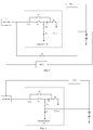
- FIG 2A is a schematic structural diagram of a charging circuit for an electronic device according to other implementations.
- the charging circuit 20 includes a control module 201, a charge pump 202, and a battery assembly 203.
- the charge pump 202 includes a first switch component S1, a second switch component S2, a third switch component S3, a fourth switch component S4, a first capacitor component C1, and a second capacitor component C2.
- An input end of the first switch component S1 and an input end of the third switch component S3 are used as an input end of the charge pump 202.
- the input end of the charge pump 202 can be coupled with one end of the control module 201, and the other end of the control module 201 can be coupled with the battery assembly 203, to achieve information interaction with the power adaptor in charging of the battery assembly by the power adaptor.
- the control module 201 monitors in real time a charging state of each cell in the battery assembly 203 and informs the charging state to the power adaptor.
- An output end of the first switch component S1 is coupled with an input end of the second switch component S2, and an output end of the second switch component S2 is grounded.
- An output end of the third switch component S3 is coupled with an input end of the first capacitor component C1 and an input end of the fourth switch component S4 respectively.
- An output end of the first capacitor component C1 is coupled with the input end of the second switch component S2.
- An output end of the fourth switch component S4 is used as an output end of the charge pump 202 and is coupled with an input end of the second capacitor component C2 and a positive electrode of the battery assembly 203 respectively.
- An output end of the second capacitor component C2 is grounded, and a negative electrode of the battery assembly 203 is grounded.
- the control module 201 is configured to generate a first control signal and send the first control signal to the charge pump 202 upon detecting that a power adaptor coupled with the charge pump 202 is an adaptor for direct charging with high voltage.
- the control module 201 is configured to generate a second control signal and send the second control signal to the charge pump 202 upon detecting that the power adaptor coupled with the charge pump 202 is an adaptor for direct charging with low voltage.
- the control module 201 may be a microcontroller unit (MCU).
- the charge pump 202 is configured to switch off the first switch component S1 and the second switch component S2, and switch on the third switch component S3 and the fourth switch component S4 upon receiving the first control signal, such that the charging voltage passes through the third switch component S3 and the fourth switch component S4 to be applied to the battery assembly 203 for direct charging.
- the charge pump in response to the first control signal, the charge pump is triggered to switch off the first switch component S1 and the second switch component S2 and switch on the third switch component S3 and the fourth switch component S4, such that the charge pump can be operable with the adaptor for direct charging with high voltage without introducing an extra circuit for direct charging with high voltage. In this way, for example, it is possible to decrease the number of devices required for the charging circuit, thereby improving charging efficiency.
- the third switch component S3 and the second switch component S2 are used as a first set of components, and the first switch component S1 and the fourth switch component S4 are used as a second set of components.
- the charge pump 202 is configured to, upon receiving the second control signal, alternately switch on the first set of components and the second set of components at a preset time interval in such a manner that an output voltage of the charge pump 202 is higher than an output voltage of the power adaptor.
- the charge pump 202 is configured to apply the output voltage of the charge pump 202 to the battery assembly 203 for charging.
- a first duration for which the first set of components is on continuously and a second duration for which the second set of components is on continuously constitutes a charging cycle.
- the first duration is generally equal to the second duration.
- the first switch component S1, the second switch component S2, the third switch component S3, and the fourth switch component S4 of the charge pump each have a duty cycle of 50%.
- the first set of components is first switched on.
- S3 and S2 are in an on-state, and S1 and S4 are in an off-state.
- the charging voltage applied to the electronic device by the power adaptor that is, an input voltage of the charge pump V in
- the third switch component S3 passes through the third switch component S3 to be applied to the first capacitor component C1 for charging.
- an input voltage of C1 is equal to the input voltage of the charge pump V in .
- the second set of components is switched on.
- S1 and S4 are in an on-state, and S2 and S3 are in an off-state.
- the output voltage of the charge pump V out is equal to a sum of the input voltage of the charge pump and the input voltage of C1, that is, the output voltage of the charge pump is twice the input voltage of the charge pump.
- working timings of switch components in the charge pump are changed, such that the charge pump can switch between the boost conversion mode and the bypass mode.
- the boost conversion mode of the charge pump is enabled.
- the power adaptor coupled with the electronic device is the adaptor for direct charging with high voltage (that is, a power adaptor of which a maximum output voltage is higher than the voltage of the battery assembly)
- the bypass mode of the charge pump is enabled.
- the charging circuit generally includes a charge pump and a circuit for direct charging with high voltage, where the charge pump is configured for boost charging with an adaptor for charging with low voltage ("low-voltage" adaptor for short), and the circuit for direct charging with high voltage is configured to support charging functions of the adaptor for direct charging with high voltage.
- the circuit for direct charging with high voltage includes a switch component S5 (such as, for example, a pair of metal oxide semiconductors (MOS) which are back-to-back) and a microcontroller unit MCU2.
- MCU2 is configured to control S5 to be switched on or switched off. In this example, a large number of devices are needed for the charging circuit, and charging efficiency can be low.
- charging of dual battery is performed by a 5V Voltage Open Loop Multi-step Constant-Current Charging ("VOOC") adaptor along with a voltage doubler charge pump.
- VOOC Voltage Open Loop Multi-step Constant-Current Charging
- the input voltage of the charge pump is V in
- an input current of the charge pump is I in
- the output voltage of the charge pump is V out
- an output current of the charge pump is I out .
- a charge pump 401 has an output end coupled with a positive electrode of the dual battery and has an input end coupled with an output end of the adaptor.
- An MCU continuously monitors a state of the dual battery and informs the state of the dual battery to the adaptor.
- the adaptor adjusts its own output according to the state of the dual battery.
- switches S1, S2, S3, and S4 in the charge pump 401 are switched on or switched off at a 50% duty cycle.
- the charge pump illustrated in FIG 4 and the charge pump illustrated in FIG 3 have the same circuit structure as the charge pump illustrated in FIG 2A to FIG 2D and therefore will not be described in detail herein again.
- the charge pump 401 When coupled with the adaptor for direct charging with low voltage, the charge pump 401 is in the boost conversion mode. When coupled with the adaptor for direct charging with high voltage, S3 and S4 in the charge pump 401 are in an on-state and S1 and S2 are in an off-state, and here, the charge pump is in the bypass mode, in which the output voltage of the adaptor is directly applied to the input end of the dual battery for direct charging. In this way, direct charging with high voltage is achieved with the charge pump 401, which can not only decrease the number of devices required for the charging circuit but also improve charging efficiency of the charging circuit.
- FIG 5 is a schematic flowchart of a charging method according to implementations. As illustrated in FIG 5 , the method can include operations at step S501 to step S505.
- a type of a power adaptor coupled with an electronic device is determined. If the power adaptor is an adaptor for direct charging with high voltage, then the method proceeds to operations at step S502. If the power adaptor is an adaptor for direct charging with low voltage, the method proceeds to operations at step S504.
- the type of the power adaptor can be determined by detecting whether a charging voltage applied to the electronic device by the power adaptor is higher than a preset threshold voltage. For example, if the charging voltage is higher than the preset threshold voltage, the power adaptor is determined to be an adaptor for direct charging with high voltage. If the charging voltage is lower than or equal to the preset threshold voltage, the power adaptor is determined to be an adaptor for direct charging with low voltage.
- step S502 a first control signal is generated, and the method proceeds to operations at step S503.
- the first control signal is used for controlling a charge pump of a charging circuit to be switched on to directly apply the charging voltage to a battery assembly for direct charging, where the battery assembly includes at least one cell.
- the charge pump of the charging circuit is controlled, according to the first control signal, to be switched on to directly apply the charging voltage to the battery assembly for direct charging.
- a second control signal is generated, and proceed to operations at step S505.
- the second control signal can control the charge pump to perform boost conversion on the charging voltage and apply the charging voltage subjected to the boost conversion to the battery assembly for charging.
- the charge pump is controlled, according to the second control signal, to perform boost conversion on the charging voltage and apply the charging voltage subjected to the boost conversion to the battery assembly for charging.
- the charge pump is controlled, according to the first control signal, to be switched on to directly apply the charging voltage to the battery assembly for direct charging as follows.
- M switch components in the charge pump are switched on according to the first control signal, such that the charging voltage passes through the M switch components to be applied to the battery assembly for direct charging, where the M switch components are located between the power adaptor and the battery assembly, and M is an integer greater than or equal to one.
- the charge pump 202 switches off the first switch component S1 and the second switch component S2, and switches on the third switch component S3 and the fourth switch component S4 according to the first control signal, such that the charging voltage passes through the third switch component S3 and the fourth switch component S4 to be applied to the battery assembly 203 for direct charging.
- the charge pump is controlled, according to the second control signal, to perform boost conversion on the charging voltage and apply the charging voltage subjected to the boost conversion to the battery assembly for charging as follows.
- Boost conversion is performed on the charging voltage according to the second control signal by using capacitor components in the charge pump and alternately switching on N switch components in the charge pump, in such a manner that an output voltage of the charge pump is higher than the charging voltage, where N is an integer greater than or equal to one.
- the output voltage is applied to the battery assembly for charging.
- the third switch component S3 and the second switch component S2 can be used as a first set of components, and the first switch component S1 and the fourth switch component S4 can be used as a second set of components.
- the charge pump 202 upon receiving the second control signal, the charge pump 202 alternately switches on the first set of components and the second set of components at a preset time interval according to the second control signal such that the output voltage of the charge pump 202 is higher than the charging voltage. Then the charge pump 202 applies the output voltage to the battery assembly for charging.
- the above charging method may be stored in a computer readable storage medium.
- the essential technical solution, or the portion that contributes to the prior art may be embodied as software products.
- the computer software products can be stored in a storage medium and may include multiple instructions that, when executed, can cause an electronic device, e.g., a mobile phone, a tablet computer, a desktop, a PDA, a GPS, a digital telephone, a video telephone, a television, a sensor device, etc. to execute some or all operations of the methods described in various implementations.
- the above storage medium may include various kinds of media that can store program codes, such as, for example, a USB flash disk, a mobile hard drive, a read only memory (ROM), a magnetic disk, or an optical disk. Therefore,there is not particular restriction on the combination of hardware and software in implementations.
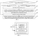
- FIG 6 is a schematic diagram illustrating hardware of an electronic device according to implementations.
- the electronic device 600 includes a memory 601 and a processor 602.
- the memory 601 is configured to store computer programs which, when executed by the processor 602, are operable with the processor 602 to perform the charging method described in the foregoing implementations.
- the memory 601 is configured to store instructions and applications operable with the processor 602 and may also cache data (such as, for example, image data, audio data, voice communication data, and video communication data) to be processed or processed by various modules in the processor 602 and the electronic device 600.
- the memory 601 may be implemented as flash memory or a random access memory (RAM).
- the computer readable storage medium is configured to store computer programs which, when executed by a processor, are operable with the processor to perform the charging method described in the foregoing implementations.
- the apparatuses, and methods disclosed in implementations herein may also be implemented in various other manners.
- the above apparatus implementations are merely illustrative, e.g., the division of units is only a division of logical functions, and there may exist other manners of division in practice, e.g., multiple units or assemblies may be combined or may be integrated into another system, or some features may be ignored or skipped.
- the coupling or direct coupling or communication connection as illustrated or discussed may be an indirect coupling or communication connection through some interface, device, or unit, and may be electrical, mechanical, or otherwise.
- Separated units as illustrated may or may not be physically separated.
- Components displayed as units may or may not be physical units, and may reside at one location or may be distributed to multiple networked units. Some or all of the units may be selectively adopted according to practical needs to achieve desired objectives of the disclosure.
- Various functional units described in implementations herein may be integrated into one processing unit or may be present as a number of physically separated units, and two or more units may be integrated into one.
- the integrated unit may take the form of hardware or hardware plus software functional unit.
- the program referred to herein may be stored in a computer-readable storage medium.
- the storage medium includes various kinds of media that can store program codes, such as, for example, a portable storage device, a ROM, a magnetic disk, or an optical disk.
- the integrated units are implemented as software functional units and sold or used as standalone products, they may be stored in a computer readable storage medium. Based on such an understanding, the essential technical solution, or the portion that contributes to the prior art may be embodied as software products.
- the computer software products can be stored in a storage medium and may include multiple instructions that, when executed, can cause an electronic device, e.g., a mobile phone, a tablet computer, a desktop, a PDA, a GPS, a digital telephone, a video telephone, a television, a sensor device, etc. to execute some or all operations of the methods described in various implementations.
- the above storage medium may include various kinds of media that can store program codes, such as a portable storage device, a ROM, a magnetic disk, or an optical disk.
- Implementations provide a charging circuit for an electronic device.
- a charging circuit for an electronic device During charging of a battery assembly of the charging circuit performed by a power adaptor electrically coupled with the electronic device, if the power adaptor is an adaptor for direct charging with high voltage, a charging voltage applied to the electronic device by the power adaptor passes through a charge pump to be applied directly to the battery assembly for direct charging, which is possible to decrease the number of devices needed for the charging circuit, thereby improving charging efficiency.
Landscapes
- Engineering & Computer Science (AREA)
- Power Engineering (AREA)
- Charge And Discharge Circuits For Batteries Or The Like (AREA)
Applications Claiming Priority (1)
| Application Number | Priority Date | Filing Date | Title |
|---|---|---|---|
| PCT/CN2019/076556 WO2020172869A1 (zh) | 2019-02-28 | 2019-02-28 | 电子设备的充电电路及方法、设备、存储介质 |
Publications (3)
| Publication Number | Publication Date |
|---|---|
| EP3761476A1 true EP3761476A1 (de) | 2021-01-06 |
| EP3761476A4 EP3761476A4 (de) | 2021-04-28 |
| EP3761476B1 EP3761476B1 (de) | 2023-01-18 |
Family
ID=72238252
Family Applications (1)
| Application Number | Title | Priority Date | Filing Date |
|---|---|---|---|
| EP19916792.5A Active EP3761476B1 (de) | 2019-02-28 | 2019-02-28 | Ladeschaltung und -verfahren für elektronische vorrichtung, vorrichtung und speichermedium |
Country Status (4)
| Country | Link |
|---|---|
| US (1) | US11502535B2 (de) |
| EP (1) | EP3761476B1 (de) |
| CN (1) | CN111869038B (de) |
| WO (1) | WO2020172869A1 (de) |
Families Citing this family (10)
| Publication number | Priority date | Publication date | Assignee | Title |
|---|---|---|---|---|
| US12388361B2 (en) * | 2020-06-02 | 2025-08-12 | Qualcomm Incorporated | Battery charging circuit and methods for trickle charging and precharging a dead multi-cell-in-series battery |
| CN114256889B (zh) * | 2020-09-21 | 2024-10-18 | Oppo(重庆)智能科技有限公司 | 充放电电路、电子设备和充放电方法 |
| CN112769177B (zh) * | 2020-12-29 | 2023-07-18 | Oppo广东移动通信有限公司 | 电源适配器、电子设备、充电系统和充电方法 |
| CN113098109A (zh) * | 2021-05-14 | 2021-07-09 | Oppo广东移动通信有限公司 | 充电电路、电子设备及充电方法 |
| CN113224822B (zh) * | 2021-05-26 | 2024-04-26 | 北京小米移动软件有限公司 | 一种充电控制方法、装置以及存储介质 |
| CN113725958A (zh) | 2021-08-17 | 2021-11-30 | 珠海市魅族科技有限公司 | 电池电源调节电路、调节方法、充电线及终端设备 |
| CN113746163B (zh) * | 2021-08-17 | 2025-01-28 | 芯海科技(深圳)股份有限公司 | 一种电源控制电路、集成电路、电源模组以及电子设备 |
| TWI764828B (zh) * | 2021-09-10 | 2022-05-11 | 禾瑞亞科技股份有限公司 | 可偵測飛跨電容短路之倍壓開關式電容電路及其偵測方法 |
| US12587021B2 (en) * | 2021-09-15 | 2026-03-24 | Halo Microelectronics International | Versatile battery charging system and control method |
| CN114079311B (zh) * | 2021-10-18 | 2025-07-22 | 联想(北京)有限公司 | 一种充电控制电路、充电控制方法及电子设备 |
Family Cites Families (17)
| Publication number | Priority date | Publication date | Assignee | Title |
|---|---|---|---|---|
| DE60027706T2 (de) * | 2000-02-15 | 2007-04-26 | Stmicroelectronics S.R.L., Agrate Brianza | Ladungspumpenschaltung und Spannungserhöhungsanordnung mit Übertragung und Gewinnung der Ladung |
| JP2005348561A (ja) * | 2004-06-04 | 2005-12-15 | Renesas Technology Corp | チャージポンプ方式電源回路 |
| US8310218B2 (en) * | 2007-08-08 | 2012-11-13 | Advanced Analogic Technologies, Inc. | Time-multiplexed-capacitor DC/DC converter with multiple outputs |
| CN101394094B (zh) * | 2007-09-20 | 2010-07-14 | 深圳市盈基实业有限公司 | 全自动高效升降压电路 |
| JP5377049B2 (ja) * | 2009-04-16 | 2013-12-25 | 矢崎総業株式会社 | 昇圧装置 |
| WO2011016463A1 (ja) * | 2009-08-03 | 2011-02-10 | 株式会社フジクラ | 太陽電池付き充電器 |
| US10374449B2 (en) * | 2014-06-04 | 2019-08-06 | Societe Bic | Smart charging portable electronic device |
| CN105896959B (zh) * | 2015-02-15 | 2019-03-08 | 天工方案公司 | 交错的双输出电荷泵 |
| CN204518162U (zh) * | 2015-04-09 | 2015-07-29 | 杭州宽福科技有限公司 | 一种电荷泵式led驱动芯片 |
| CN105244970B (zh) * | 2015-11-06 | 2017-08-29 | 无锡中感微电子股份有限公司 | 充电电路 |
| JP6668799B2 (ja) * | 2016-02-12 | 2020-03-18 | セイコーエプソン株式会社 | 電子機器 |
| US10516284B2 (en) * | 2016-09-15 | 2019-12-24 | Qualcomm Incorporated | Voltage controlled charge pump and battery charger |
| US10797500B2 (en) * | 2016-09-20 | 2020-10-06 | Richtek Technology Corporation | Charger circuit and capacitive power conversion circuit and charging control method thereof |
| CN107947252B (zh) * | 2016-10-12 | 2020-09-22 | Oppo广东移动通信有限公司 | 终端和设备 |
| US10284090B2 (en) * | 2016-10-20 | 2019-05-07 | Cirrus Logic, Inc. | Combined boost converter and power converter |
| EP3561990B1 (de) * | 2017-02-24 | 2020-11-04 | Guangdong Oppo Mobile Telecommunications Corp., Ltd. | Entzerrungsschaltung, aufzuladende vorrichtung und ladesteuerungsverfahren |
| CN108233460B (zh) * | 2017-09-04 | 2021-10-22 | 珠海市魅族科技有限公司 | 一种充电方法、充电装置及终端设备 |
-
2019
- 2019-02-28 CN CN201980003862.0A patent/CN111869038B/zh active Active
- 2019-02-28 WO PCT/CN2019/076556 patent/WO2020172869A1/zh not_active Ceased
- 2019-02-28 EP EP19916792.5A patent/EP3761476B1/de active Active
-
2020
- 2020-06-04 US US16/893,006 patent/US11502535B2/en active Active
Also Published As
| Publication number | Publication date |
|---|---|
| US11502535B2 (en) | 2022-11-15 |
| US20200303927A1 (en) | 2020-09-24 |
| CN111869038A (zh) | 2020-10-30 |
| WO2020172869A1 (zh) | 2020-09-03 |
| CN111869038B (zh) | 2021-06-04 |
| EP3761476B1 (de) | 2023-01-18 |
| EP3761476A4 (de) | 2021-04-28 |
Similar Documents
| Publication | Publication Date | Title |
|---|---|---|
| US11502535B2 (en) | Charging circuit for electronic device, charging method, and electronic device | |
| JP5791007B2 (ja) | 電力供給の装置および方法ならびにユーザ装置 | |
| US10788903B2 (en) | Signal generating circuit of active pen, active pen and signal driving method | |
| CN103138376B (zh) | 电源切换电路及其电源切换方法 | |
| CN112787374A (zh) | 充电系统、电子设备及其充电控制方法 | |
| CN112701751B (zh) | 供电电路、供电方法和电子设备 | |
| US12388361B2 (en) | Battery charging circuit and methods for trickle charging and precharging a dead multi-cell-in-series battery | |
| WO2023143381A1 (zh) | 闪光灯电路、控制方法、电子设备及可读存储介质 | |
| CN112234704B (zh) | 闪光灯电源切换电路、闪光灯控制方法及电子设备 | |
| WO2014116823A2 (en) | Boost converter topology for high efficiency and low battery voltage support | |
| CN113763879B (zh) | 供电电路、显示屏、电子设备及供电控制方法 | |
| WO2025228034A1 (zh) | 双接口切换电路、方法以及上网装置 | |
| CN108811279A (zh) | 闪光灯的驱动方法及电子设备 | |
| CN112640288B (zh) | 一种正负压打码电路、芯片、主动笔以及打码方法 | |
| CN115296384B (zh) | 自举电容充电方法、装置、计算机设备和存储介质 | |
| CN114069768B (zh) | 充电电路、充电控制方法、装置和电子设备 | |
| CN112821475A (zh) | 充电电路、充电控制方法及装置 | |
| WO2016161746A1 (zh) | 电源供电电路及供电方法 | |
| CN119209416A (zh) | 防护电路和相关装置 | |
| CN114465294B (zh) | 电源管理模块和电子设备 | |
| CN103095929B (zh) | 一种防止移动终端不停重启的方法、系统及移动终端 | |
| WO2021023293A1 (zh) | 充电电路、充电芯片、终端和充电系统 | |
| CN113746148A (zh) | 电源组件、电子设备、充电控制方法、装置及存储介质 | |
| CN105284028A (zh) | 一种充电装置及充电方法 | |
| CN216751268U (zh) | 供电电路及终端设备 |
Legal Events
| Date | Code | Title | Description |
|---|---|---|---|
| STAA | Information on the status of an ep patent application or granted ep patent |
Free format text: STATUS: THE INTERNATIONAL PUBLICATION HAS BEEN MADE |
|
| PUAI | Public reference made under article 153(3) epc to a published international application that has entered the european phase |
Free format text: ORIGINAL CODE: 0009012 |
|
| STAA | Information on the status of an ep patent application or granted ep patent |
Free format text: STATUS: REQUEST FOR EXAMINATION WAS MADE |
|
| 17P | Request for examination filed |
Effective date: 20200929 |
|
| AK | Designated contracting states |
Kind code of ref document: A1 Designated state(s): AL AT BE BG CH CY CZ DE DK EE ES FI FR GB GR HR HU IE IS IT LI LT LU LV MC MK MT NL NO PL PT RO RS SE SI SK SM TR |
|
| AX | Request for extension of the european patent |
Extension state: BA ME |
|
| A4 | Supplementary search report drawn up and despatched |
Effective date: 20210330 |
|
| RIC1 | Information provided on ipc code assigned before grant |
Ipc: H02J 7/00 20060101AFI20210324BHEP |
|
| STAA | Information on the status of an ep patent application or granted ep patent |
Free format text: STATUS: EXAMINATION IS IN PROGRESS |
|
| 17Q | First examination report despatched |
Effective date: 20210923 |
|
| DAV | Request for validation of the european patent (deleted) | ||
| DAX | Request for extension of the european patent (deleted) | ||
| GRAP | Despatch of communication of intention to grant a patent |
Free format text: ORIGINAL CODE: EPIDOSNIGR1 |
|
| STAA | Information on the status of an ep patent application or granted ep patent |
Free format text: STATUS: GRANT OF PATENT IS INTENDED |
|
| INTG | Intention to grant announced |
Effective date: 20221103 |
|
| GRAS | Grant fee paid |
Free format text: ORIGINAL CODE: EPIDOSNIGR3 |
|
| GRAA | (expected) grant |
Free format text: ORIGINAL CODE: 0009210 |
|
| STAA | Information on the status of an ep patent application or granted ep patent |
Free format text: STATUS: THE PATENT HAS BEEN GRANTED |
|
| AK | Designated contracting states |
Kind code of ref document: B1 Designated state(s): AL AT BE BG CH CY CZ DE DK EE ES FI FR GB GR HR HU IE IS IT LI LT LU LV MC MK MT NL NO PL PT RO RS SE SI SK SM TR |
|
| REG | Reference to a national code |
Ref country code: GB Ref legal event code: FG4D |
|
| REG | Reference to a national code |
Ref country code: DE Ref legal event code: R096 Ref document number: 602019024668 Country of ref document: DE |
|
| REG | Reference to a national code |
Ref country code: CH Ref legal event code: EP |
|
| REG | Reference to a national code |
Ref country code: AT Ref legal event code: REF Ref document number: 1545210 Country of ref document: AT Kind code of ref document: T Effective date: 20230215 Ref country code: IE Ref legal event code: FG4D |
|
| PGFP | Annual fee paid to national office [announced via postgrant information from national office to epo] |
Ref country code: FR Payment date: 20230221 Year of fee payment: 5 |
|
| REG | Reference to a national code |
Ref country code: LT Ref legal event code: MG9D |
|
| REG | Reference to a national code |
Ref country code: NL Ref legal event code: MP Effective date: 20230118 |
|
| P01 | Opt-out of the competence of the unified patent court (upc) registered |
Effective date: 20230412 |
|
| REG | Reference to a national code |
Ref country code: AT Ref legal event code: MK05 Ref document number: 1545210 Country of ref document: AT Kind code of ref document: T Effective date: 20230118 |
|
| PG25 | Lapsed in a contracting state [announced via postgrant information from national office to epo] |
Ref country code: NL Free format text: LAPSE BECAUSE OF FAILURE TO SUBMIT A TRANSLATION OF THE DESCRIPTION OR TO PAY THE FEE WITHIN THE PRESCRIBED TIME-LIMIT Effective date: 20230118 |
|
| PG25 | Lapsed in a contracting state [announced via postgrant information from national office to epo] |
Ref country code: RS Free format text: LAPSE BECAUSE OF FAILURE TO SUBMIT A TRANSLATION OF THE DESCRIPTION OR TO PAY THE FEE WITHIN THE PRESCRIBED TIME-LIMIT Effective date: 20230118 Ref country code: PT Free format text: LAPSE BECAUSE OF FAILURE TO SUBMIT A TRANSLATION OF THE DESCRIPTION OR TO PAY THE FEE WITHIN THE PRESCRIBED TIME-LIMIT Effective date: 20230518 Ref country code: NO Free format text: LAPSE BECAUSE OF FAILURE TO SUBMIT A TRANSLATION OF THE DESCRIPTION OR TO PAY THE FEE WITHIN THE PRESCRIBED TIME-LIMIT Effective date: 20230418 Ref country code: LV Free format text: LAPSE BECAUSE OF FAILURE TO SUBMIT A TRANSLATION OF THE DESCRIPTION OR TO PAY THE FEE WITHIN THE PRESCRIBED TIME-LIMIT Effective date: 20230118 Ref country code: LT Free format text: LAPSE BECAUSE OF FAILURE TO SUBMIT A TRANSLATION OF THE DESCRIPTION OR TO PAY THE FEE WITHIN THE PRESCRIBED TIME-LIMIT Effective date: 20230118 Ref country code: HR Free format text: LAPSE BECAUSE OF FAILURE TO SUBMIT A TRANSLATION OF THE DESCRIPTION OR TO PAY THE FEE WITHIN THE PRESCRIBED TIME-LIMIT Effective date: 20230118 Ref country code: ES Free format text: LAPSE BECAUSE OF FAILURE TO SUBMIT A TRANSLATION OF THE DESCRIPTION OR TO PAY THE FEE WITHIN THE PRESCRIBED TIME-LIMIT Effective date: 20230118 Ref country code: AT Free format text: LAPSE BECAUSE OF FAILURE TO SUBMIT A TRANSLATION OF THE DESCRIPTION OR TO PAY THE FEE WITHIN THE PRESCRIBED TIME-LIMIT Effective date: 20230118 |
|
| PG25 | Lapsed in a contracting state [announced via postgrant information from national office to epo] |
Ref country code: SE Free format text: LAPSE BECAUSE OF FAILURE TO SUBMIT A TRANSLATION OF THE DESCRIPTION OR TO PAY THE FEE WITHIN THE PRESCRIBED TIME-LIMIT Effective date: 20230118 Ref country code: PL Free format text: LAPSE BECAUSE OF FAILURE TO SUBMIT A TRANSLATION OF THE DESCRIPTION OR TO PAY THE FEE WITHIN THE PRESCRIBED TIME-LIMIT Effective date: 20230118 Ref country code: IS Free format text: LAPSE BECAUSE OF FAILURE TO SUBMIT A TRANSLATION OF THE DESCRIPTION OR TO PAY THE FEE WITHIN THE PRESCRIBED TIME-LIMIT Effective date: 20230518 Ref country code: GR Free format text: LAPSE BECAUSE OF FAILURE TO SUBMIT A TRANSLATION OF THE DESCRIPTION OR TO PAY THE FEE WITHIN THE PRESCRIBED TIME-LIMIT Effective date: 20230419 Ref country code: FI Free format text: LAPSE BECAUSE OF FAILURE TO SUBMIT A TRANSLATION OF THE DESCRIPTION OR TO PAY THE FEE WITHIN THE PRESCRIBED TIME-LIMIT Effective date: 20230118 |
|
| REG | Reference to a national code |
Ref country code: CH Ref legal event code: PL |
|
| REG | Reference to a national code |
Ref country code: DE Ref legal event code: R097 Ref document number: 602019024668 Country of ref document: DE Ref country code: BE Ref legal event code: MM Effective date: 20230228 |
|
| PG25 | Lapsed in a contracting state [announced via postgrant information from national office to epo] |
Ref country code: SM Free format text: LAPSE BECAUSE OF FAILURE TO SUBMIT A TRANSLATION OF THE DESCRIPTION OR TO PAY THE FEE WITHIN THE PRESCRIBED TIME-LIMIT Effective date: 20230118 Ref country code: RO Free format text: LAPSE BECAUSE OF FAILURE TO SUBMIT A TRANSLATION OF THE DESCRIPTION OR TO PAY THE FEE WITHIN THE PRESCRIBED TIME-LIMIT Effective date: 20230118 Ref country code: MC Free format text: LAPSE BECAUSE OF FAILURE TO SUBMIT A TRANSLATION OF THE DESCRIPTION OR TO PAY THE FEE WITHIN THE PRESCRIBED TIME-LIMIT Effective date: 20230118 Ref country code: LU Free format text: LAPSE BECAUSE OF NON-PAYMENT OF DUE FEES Effective date: 20230228 Ref country code: LI Free format text: LAPSE BECAUSE OF NON-PAYMENT OF DUE FEES Effective date: 20230228 Ref country code: EE Free format text: LAPSE BECAUSE OF FAILURE TO SUBMIT A TRANSLATION OF THE DESCRIPTION OR TO PAY THE FEE WITHIN THE PRESCRIBED TIME-LIMIT Effective date: 20230118 Ref country code: DK Free format text: LAPSE BECAUSE OF FAILURE TO SUBMIT A TRANSLATION OF THE DESCRIPTION OR TO PAY THE FEE WITHIN THE PRESCRIBED TIME-LIMIT Effective date: 20230118 Ref country code: CZ Free format text: LAPSE BECAUSE OF FAILURE TO SUBMIT A TRANSLATION OF THE DESCRIPTION OR TO PAY THE FEE WITHIN THE PRESCRIBED TIME-LIMIT Effective date: 20230118 Ref country code: CH Free format text: LAPSE BECAUSE OF NON-PAYMENT OF DUE FEES Effective date: 20230228 |
|
| PLBE | No opposition filed within time limit |
Free format text: ORIGINAL CODE: 0009261 |
|
| STAA | Information on the status of an ep patent application or granted ep patent |
Free format text: STATUS: NO OPPOSITION FILED WITHIN TIME LIMIT |
|
| PG25 | Lapsed in a contracting state [announced via postgrant information from national office to epo] |
Ref country code: SK Free format text: LAPSE BECAUSE OF FAILURE TO SUBMIT A TRANSLATION OF THE DESCRIPTION OR TO PAY THE FEE WITHIN THE PRESCRIBED TIME-LIMIT Effective date: 20230118 |
|
| REG | Reference to a national code |
Ref country code: IE Ref legal event code: MM4A |
|
| 26N | No opposition filed |
Effective date: 20231019 |
|
| PG25 | Lapsed in a contracting state [announced via postgrant information from national office to epo] |
Ref country code: SI Free format text: LAPSE BECAUSE OF FAILURE TO SUBMIT A TRANSLATION OF THE DESCRIPTION OR TO PAY THE FEE WITHIN THE PRESCRIBED TIME-LIMIT Effective date: 20230118 Ref country code: IE Free format text: LAPSE BECAUSE OF NON-PAYMENT OF DUE FEES Effective date: 20230228 |
|
| PG25 | Lapsed in a contracting state [announced via postgrant information from national office to epo] |
Ref country code: BE Free format text: LAPSE BECAUSE OF NON-PAYMENT OF DUE FEES Effective date: 20230228 |
|
| PG25 | Lapsed in a contracting state [announced via postgrant information from national office to epo] |
Ref country code: IT Free format text: LAPSE BECAUSE OF FAILURE TO SUBMIT A TRANSLATION OF THE DESCRIPTION OR TO PAY THE FEE WITHIN THE PRESCRIBED TIME-LIMIT Effective date: 20230118 |
|
| PG25 | Lapsed in a contracting state [announced via postgrant information from national office to epo] |
Ref country code: BG Free format text: LAPSE BECAUSE OF FAILURE TO SUBMIT A TRANSLATION OF THE DESCRIPTION OR TO PAY THE FEE WITHIN THE PRESCRIBED TIME-LIMIT Effective date: 20230118 |
|
| PG25 | Lapsed in a contracting state [announced via postgrant information from national office to epo] |
Ref country code: BG Free format text: LAPSE BECAUSE OF FAILURE TO SUBMIT A TRANSLATION OF THE DESCRIPTION OR TO PAY THE FEE WITHIN THE PRESCRIBED TIME-LIMIT Effective date: 20230118 |
|
| PG25 | Lapsed in a contracting state [announced via postgrant information from national office to epo] |
Ref country code: FR Free format text: LAPSE BECAUSE OF NON-PAYMENT OF DUE FEES Effective date: 20240229 |
|
| PG25 | Lapsed in a contracting state [announced via postgrant information from national office to epo] |
Ref country code: FR Free format text: LAPSE BECAUSE OF NON-PAYMENT OF DUE FEES Effective date: 20240229 |
|
| PG25 | Lapsed in a contracting state [announced via postgrant information from national office to epo] |
Ref country code: CY Free format text: LAPSE BECAUSE OF FAILURE TO SUBMIT A TRANSLATION OF THE DESCRIPTION OR TO PAY THE FEE WITHIN THE PRESCRIBED TIME-LIMIT; INVALID AB INITIO Effective date: 20190228 |
|
| PG25 | Lapsed in a contracting state [announced via postgrant information from national office to epo] |
Ref country code: HU Free format text: LAPSE BECAUSE OF FAILURE TO SUBMIT A TRANSLATION OF THE DESCRIPTION OR TO PAY THE FEE WITHIN THE PRESCRIBED TIME-LIMIT; INVALID AB INITIO Effective date: 20190228 |
|
| PG25 | Lapsed in a contracting state [announced via postgrant information from national office to epo] |
Ref country code: TR Free format text: LAPSE BECAUSE OF FAILURE TO SUBMIT A TRANSLATION OF THE DESCRIPTION OR TO PAY THE FEE WITHIN THE PRESCRIBED TIME-LIMIT Effective date: 20230118 |
|
| PGFP | Annual fee paid to national office [announced via postgrant information from national office to epo] |
Ref country code: GB Payment date: 20260224 Year of fee payment: 8 |
|
| PGFP | Annual fee paid to national office [announced via postgrant information from national office to epo] |
Ref country code: DE Payment date: 20260223 Year of fee payment: 8 |