EP3761509A1 - Circuit à boucle à verrouillage de phase - Google Patents
Circuit à boucle à verrouillage de phase Download PDFInfo
- Publication number
- EP3761509A1 EP3761509A1 EP19761589.1A EP19761589A EP3761509A1 EP 3761509 A1 EP3761509 A1 EP 3761509A1 EP 19761589 A EP19761589 A EP 19761589A EP 3761509 A1 EP3761509 A1 EP 3761509A1
- Authority
- EP
- European Patent Office
- Prior art keywords
- capacitor
- voltage
- current source
- current
- phase
- Prior art date
- Legal status (The legal status is an assumption and is not a legal conclusion. Google has not performed a legal analysis and makes no representation as to the accuracy of the status listed.)
- Pending
Links
- 239000003990 capacitor Substances 0.000 claims abstract description 126
- 238000005516 engineering process Methods 0.000 abstract description 22
- 238000004891 communication Methods 0.000 abstract description 10
- 238000010586 diagram Methods 0.000 description 27
- 230000000630 rising effect Effects 0.000 description 20
- 230000005540 biological transmission Effects 0.000 description 12
- 230000004048 modification Effects 0.000 description 8
- 238000012986 modification Methods 0.000 description 8
- 238000010606 normalization Methods 0.000 description 7
- 230000000694 effects Effects 0.000 description 5
- 238000006243 chemical reaction Methods 0.000 description 4
- 229920000729 poly(L-lysine) polymer Polymers 0.000 description 3
- 230000002730 additional effect Effects 0.000 description 1
- 230000004075 alteration Effects 0.000 description 1
- 239000013078 crystal Substances 0.000 description 1
- 230000001934 delay Effects 0.000 description 1
- 238000001514 detection method Methods 0.000 description 1
- 238000011065 in-situ storage Methods 0.000 description 1
- 230000010354 integration Effects 0.000 description 1
- 230000010355 oscillation Effects 0.000 description 1
- 230000001151 other effect Effects 0.000 description 1
Images






Classifications
-
- H—ELECTRICITY
- H03—ELECTRONIC CIRCUITRY
- H03L—AUTOMATIC CONTROL, STARTING, SYNCHRONISATION OR STABILISATION OF GENERATORS OF ELECTRONIC OSCILLATIONS OR PULSES
- H03L7/00—Automatic control of frequency or phase; Synchronisation
- H03L7/06—Automatic control of frequency or phase; Synchronisation using a reference signal applied to a frequency- or phase-locked loop
- H03L7/08—Details of the phase-locked loop
- H03L7/085—Details of the phase-locked loop concerning mainly the frequency- or phase-detection arrangement including the filtering or amplification of its output signal
- H03L7/089—Details of the phase-locked loop concerning mainly the frequency- or phase-detection arrangement including the filtering or amplification of its output signal the phase or frequency detector generating up-down pulses
- H03L7/0891—Details of the phase-locked loop concerning mainly the frequency- or phase-detection arrangement including the filtering or amplification of its output signal the phase or frequency detector generating up-down pulses the up-down pulses controlling source and sink current generators, e.g. a charge pump
- H03L7/0895—Details of the current generators
-
- H—ELECTRICITY
- H03—ELECTRONIC CIRCUITRY
- H03L—AUTOMATIC CONTROL, STARTING, SYNCHRONISATION OR STABILISATION OF GENERATORS OF ELECTRONIC OSCILLATIONS OR PULSES
- H03L7/00—Automatic control of frequency or phase; Synchronisation
- H03L7/06—Automatic control of frequency or phase; Synchronisation using a reference signal applied to a frequency- or phase-locked loop
- H03L7/08—Details of the phase-locked loop
- H03L7/085—Details of the phase-locked loop concerning mainly the frequency- or phase-detection arrangement including the filtering or amplification of its output signal
- H03L7/091—Details of the phase-locked loop concerning mainly the frequency- or phase-detection arrangement including the filtering or amplification of its output signal the phase or frequency detector using a sampling device
-
- H—ELECTRICITY
- H03—ELECTRONIC CIRCUITRY
- H03K—PULSE TECHNIQUE
- H03K5/00—Manipulating of pulses not covered by one of the other main groups of this subclass
- H03K5/22—Circuits having more than one input and one output for comparing pulses or pulse trains with each other according to input signal characteristics, e.g. slope, integral
- H03K5/26—Circuits having more than one input and one output for comparing pulses or pulse trains with each other according to input signal characteristics, e.g. slope, integral the characteristic being duration, interval, position, frequency, or sequence
-
- H—ELECTRICITY
- H03—ELECTRONIC CIRCUITRY
- H03L—AUTOMATIC CONTROL, STARTING, SYNCHRONISATION OR STABILISATION OF GENERATORS OF ELECTRONIC OSCILLATIONS OR PULSES
- H03L7/00—Automatic control of frequency or phase; Synchronisation
- H03L7/06—Automatic control of frequency or phase; Synchronisation using a reference signal applied to a frequency- or phase-locked loop
- H03L7/08—Details of the phase-locked loop
- H03L7/085—Details of the phase-locked loop concerning mainly the frequency- or phase-detection arrangement including the filtering or amplification of its output signal
-
- H—ELECTRICITY
- H03—ELECTRONIC CIRCUITRY
- H03M—CODING; DECODING; CODE CONVERSION IN GENERAL
- H03M3/00—Conversion of analogue values to or from differential modulation
- H03M3/30—Delta-sigma modulation
- H03M3/39—Structural details of delta-sigma modulators, e.g. incremental delta-sigma modulators
- H03M3/412—Structural details of delta-sigma modulators, e.g. incremental delta-sigma modulators characterised by the number of quantisers and their type and resolution
- H03M3/422—Structural details of delta-sigma modulators, e.g. incremental delta-sigma modulators characterised by the number of quantisers and their type and resolution having one quantiser only
- H03M3/424—Structural details of delta-sigma modulators, e.g. incremental delta-sigma modulators characterised by the number of quantisers and their type and resolution having one quantiser only the quantiser being a multiple bit one
- H03M3/426—Structural details of delta-sigma modulators, e.g. incremental delta-sigma modulators characterised by the number of quantisers and their type and resolution having one quantiser only the quantiser being a multiple bit one the quantiser being a successive approximation type analogue/digital converter
-
- H—ELECTRICITY
- H03—ELECTRONIC CIRCUITRY
- H03M—CODING; DECODING; CODE CONVERSION IN GENERAL
- H03M1/00—Analogue/digital conversion; Digital/analogue conversion
- H03M1/12—Analogue/digital converters
- H03M1/34—Analogue value compared with reference values
- H03M1/38—Analogue value compared with reference values sequentially only, e.g. successive approximation type
- H03M1/46—Analogue value compared with reference values sequentially only, e.g. successive approximation type with digital/analogue converter for supplying reference values to converter
- H03M1/466—Analogue value compared with reference values sequentially only, e.g. successive approximation type with digital/analogue converter for supplying reference values to converter using switched capacitors
Definitions
- the present technology relates to a phase-locked loop, and more particularly, relates to a phase-locked loop that allows a reduction in power consumption.
- the ADPLL includes a counter circuit that detects an integer phase difference between a DCO frequency signal Fdco and a reference frequency signal Fref, and a time-to-digital converter (TDC) circuit that detects a fractional phase difference.
- the counter circuit detects an integer phase difference by counting how many periods of Fdco are input within one period of Fref, and thus must be operating at all times for one period of Fref.
- the TDC circuit only needs to detect a phase difference between edges of Fref and Fdco, and thus does not need to continue operating at all times for one period of Fref, and can operate intermittently. The intermittent operation reduces average current consumption per hour, and thus allows power reduction.
- the TDC circuit delays Fdco in several inverter circuit stages, and catches a rising edge of Fref with a latch circuit, thereby detecting a phase difference.
- This configuration is simple but difficult to operate at low power because it needs to operate a large number of inverter circuits to generate a delay when the phase difference between Fref and Fdco is large, leading to an increase in current consumption.
- Non-Patent Document 1 proposes a TDC circuit designed to remedy increased power consumption.
- the TDC circuit generates a signal of a phase difference between Fref and Fdco in a phase detector (PD), and charges a capacitor C1 with current from a charge pump (CP) for the time of the phase difference signal to obtain a voltage VF.
- PD phase detector
- CP charge pump
- the TDC circuit charges a capacitor C2 with current from the CP to generate a voltage V RAMP , and counts the number of pulses of Fdco (count number: n) until the voltage VF and the voltage V RAMP intersect in a single-slope ADC (SS-ADC).
- the capacitor C1 and the capacitor C2 are 1 : N.
- the slopes of the voltage VF and the voltage V RAMP are N : 1.
- n/N is an AD converted value and is a phase difference between Fref and Fdco.
- Non-Patent Document 1 Somnath Kundu, Bongjin Kim, Chris H. Kim, "19.2 A 0.2-to-1.45 GHz Subsampling Fractional-N All-Digital MDLL with Zero-Offset Aperture PD-Based Spur Cancellation and In-Situ Timing Mismatch Detection", 2016 IEEE International Solid-State Circuits Conference, February 3, 2016, [online] [searched on January 25, 2018], the Internet ⁇ URL: http://www.ee.umn.edu/groups/VLSIresearch/papers/2017/ISSCC16 MDLL.pdf >
- Non-Patent Document 1 when the phase difference between Fref and Fdco is large, it is necessary for the CP to continue operating for several Fdco clocks before the voltage VF and the voltage V RAMP are obtained. Consequently, the intermittent rate during one period of Fref becomes low, making it difficult to sufficiently reduce power.
- the present technology has been made in view of such circumstances, and allows a reduction in power consumption.
- a phase-locked loop includes a SAR-ADC that includes two capacitors and outputs a result of comparison between voltages generated from the two capacitors, a current source that charges the two capacitors with current, a first switch that is disposed between one of the two capacitors and the current source and is provided with a phase difference between a first clock of a reference frequency and a second clock having a higher frequency than the first clock, and a second switch that is disposed between another of the two capacitors and the current source and is provided with the second clock.
- a SAR-ADC that includes two capacitors and outputs a result of comparison between voltages generated from the two capacitors, a current source that charges the two capacitors with current, a first switch that is disposed between one of the two capacitors and the current source and is provided with a phase difference between a first clock of a reference frequency and a second clock having a higher frequency than the first clock, and a second switch that is disposed between another of the two capacitors and the current source and is provided with the second clock are included.
- effects described in the present description are merely examples.
- the effects of the present technology are not limited to the effects described in the present description, and may include additional effects.
- Fig. 1 is a block diagram illustrating a configuration example of an all-digital PLL (ADPLL) as a phase-locked loop to which the present technology is applied.
- ADPLL all-digital PLL
- the DCO frequency is a frequency higher than the reference frequency.
- the digital set frequency data FCW is data used to set the DCO frequency, and is provided from a control unit of a device including the ADPLL 1 or the like.
- the ADPLL 1 includes a counter circuit 11, a time-to-digital counter (TDC) circuit 12, a digital arithmetic circuit 13, and a voltage-controlled oscillator (VCO) 14.
- TDC time-to-digital counter
- VCO voltage-controlled oscillator
- the reference frequency signal Fref is provided to the counter circuit 11 and the TDC circuit 12.
- the digital set frequency data FCW is provided to the digital arithmetic circuit 13.
- the counter circuit 11 detects an integer phase difference between the reference frequency signal Fref provided externally and the DCO frequency signal Fdco provided from the VCO 14, and outputs a signal representing the detected integer phase difference to the digital arithmetic circuit 13.
- the TDC circuit 12 detects a fractional phase difference between the reference frequency signal Fref provided externally and the DCO frequency signal Fdco provided from the VCO 14, and outputs a signal representing the detected fractional phase difference to the digital arithmetic circuit 13.
- the digital arithmetic circuit 13 compares the signals representing the phase differences provided from the counter circuit 11 and the TDC circuit 12 with phase information obtained by time integration of the digital set frequency data FCW, and outputs the comparison result to the VCO 14 through a digital filter.
- the VCO 14 outputs a signal of an oscillation frequency according to the comparison result provided from the digital arithmetic circuit 13 to a subsequent stage (not illustrated) as the DCO frequency signal Fdco.
- the DCO frequency signal Fdco is fed back to the counter circuit 11 and the TDC circuit 12.
- Fig. 2 is a diagram illustrating the operation of the ADPLL.
- a signal waveform of the reference frequency signal Fref, a signal waveform of the DCO frequency signal Fdco, an integer phase detected in the counter circuit 11, and a fractional phase detected in the TDC circuit 12 are illustrated in the order from top.
- the values of the integer phase + the fractional phase and the values of integral multiples of the digital set frequency data FCW on which phase comparison is performed in the digital arithmetic circuit 13 are illustrated.
- the digital arithmetic circuit 13 performs a phase comparison between integer phase + fractional phase "0" and integer multiple "0" of the digital set frequency data FCW.
- the digital arithmetic circuit 13 performs a phase comparison between integer phase + fractional phase "3.2" and integer multiple "3.2" of the digital set frequency data FCW.
- the digital arithmetic circuit 13 performs a phase comparison between integer phase + fractional phase "6.4" and integer multiple "6.4" of the digital set frequency data FCW.
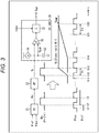
- Fig. 3 is a diagram illustrating a conventional TDC circuit for comparison with the present technology.
- a TDC circuit illustrated in Fig. 3 includes a phase-locked loop (PD) 21, a charge pump (CP) 22, and a single-slope ADC (SS-ADC) 23.
- PD phase-locked loop
- CP charge pump
- SS-ADC single-slope ADC
- the PD 21 generates a phase difference signal ⁇ F (0 to 2 ⁇ ) between a reference frequency signal Fref and a DCO frequency signal Fdco.
- phase difference signal ⁇ F While the phase difference signal ⁇ F is provided, the CP 22 charges a capacitor C1 (not illustrated) provided inside with current.
- the voltage VF output from the capacitor C1 is provided to the comparator 32.
- the current source 31 charges the capacitor C2 with current.
- a voltage V RAMP that is a period information voltage generated in the capacitor C2 due to the current charging of the current source 31 is output to the comparator 32.
- the comparator 32 compares the voltage VF and the voltage V RAMP , and outputs the comparison result to the integrator 33.
- the integrator 33 counts the number of pulses of the DCO frequency signal Fdco until the voltage VF and the voltage V RAMP intersect (count number: n (n ⁇ 1)), and outputs an operation result D out .
- n/N is an AD converted value, and is the phase difference between the reference frequency signal Fref and the DCO frequency signal Fdco.
- Fig. 3 illustrates, below the configuration diagram, a signal waveform of the phase difference signal ⁇ F , a signal waveform of the DCO frequency signal Fdco, a signal waveform of the reference frequency signal Fref, a Slope of the voltage VF generated in the capacitor C1, and a Slope of the voltage V RAMP generated in the capacitor C2 (Slope ratio N : 1).
- the PD 21 generates the phase difference signal ⁇ F for the period between the time t2 of a rising edge of the reference frequency signal Fref and the time t3 of a subsequent rising edge of the DCO frequency signal Fdco, and outputs it to the CP 22.
- the CP 22 charges the capacitor C1 with current while the phase difference signal ⁇ F is provided, that is, between the time t12 of a rising edge of the phase difference signal ⁇ F and the time t13 of a subsequent rising edge of the DCO frequency signal Fdco, so that the voltage VF is generated in the capacitor C1.
- the capacitor C2 is charged with current from the current source 31, so that the voltage V RAMP is generated in the capacitor C2.
- the integrator 33 counts the number of pulses of the DCO frequency signal Fdco (2 in the case of Fig. 1 ) (count number: n (n ⁇ 1)) until the voltage V RAMP matches the voltage VF in the comparator 32. At the time t32 of a rising edge of the DCO frequency signal Fdco when the voltage V RAMP matches the voltage VF, the charging of the capacitor C2 with current from the current source 31 is finished, and the integrator 33 finishes counting and outputs the operation result D out .
- Fig. 4 is a diagram illustrating how to determine the fractional phase difference between the reference frequency signal Fref and the DCO frequency signal Fdco.
- Fig. 4 illustrates a case with Slope ratio 4 : 1.
- the upper row illustrates an example when the phase difference signal ⁇ F is ⁇ /2, the DCO frequency signal Fdco is 2 ⁇ , and the operation result D out is 1. That is, a value of 0.25 obtained by dividing one count of the DCO frequency signal Fdco by four is the value of the phase difference signal ⁇ F .
- the middle row illustrates an example when the phase difference signal ⁇ F is ⁇ , the DCO frequency signal Fdco is 2 ⁇ , and the operation result D out is 2. That is, a value of 0.5 obtained by dividing two counts of the DCO frequency signal Fdco by four is the value of the phase difference signal ⁇ F .
- the lower row illustrates an example when the phase difference signal ⁇ F is 2 ⁇ , the DCO frequency signal Fdco is 2 ⁇ , and the operation result D out is 4. That is, a value of 1 obtained by dividing four counts of the DCO frequency signal Fdco by four is the value of the phase difference signal ⁇ F .
- the TDC circuit illustrated in Fig. 5 includes a CP 22, an SS-ADC 23, and a normalization unit 51.
- the ranges of arrows at the bottom indicate the configurations of the parts, and a PD 21 is omitted.
- the CP 22 includes a current source 31, a switch 41, and a capacitor CF.
- the SS-ADC 23 includes the current source 31, a switch 42, a capacitor C R , a comparator 32, a latch circuit 43, an integrator 33, a latch circuit 44, a latch circuit 45, and an arithmetic unit 46.
- the current source 31 includes transistors M p1 and M p2 , and is shared by the CP 22 and the SS-ADC 23 by means of switching of the switches 41 and 42.
- phase difference signal ⁇ F While a phase difference signal ⁇ F is provided, the switch 41 is turned on, and the capacitor CF is charged with current from the current source 31. The resulting voltage VF in the capacitor CF is provided to the comparator 32.
- the comparator 32 compares the voltage VF and the voltage V RAMP , and if the voltage VF and the voltage V RAMP match, it outputs a Stop signal to the latch circuit 43.
- the latch circuit 43 When the latch circuit 43 is provided with a Start signal that is output at the end of provision of the phase difference signal ⁇ F , it outputs the enable signal EN to the switch 42.
- the integrator 33 counts the number of pulses of the DCO frequency signal Fdco, and outputs the count number to the latch circuits 44 and 45.
- the latch circuit 44 holds the count number when it is provided with the Start signal that is output at the end of provision of the phase difference signal ⁇ F (14 in Fig. 6 described later), and outputs it to the arithmetic unit 46 at a predetermined timing.
- the latch circuit 45 holds the count number when it is provided with the Stop signal output from the comparator 32 (83 in Fig. 6 described later), and outputs it to the arithmetic unit 46 at a predetermined timing.
- the arithmetic unit 46 outputs, to the normalization unit 51, an operation result D out that is a difference between the value provided from the latch circuit 44 and the value provided from the latch circuit 45.
- the normalization unit 51 includes a multiplier 47.
- the multiplier 47 outputs, to a subsequent stage, a normalization result DF obtained by multiplying the operation result D out provided from the arithmetic unit 46 by 1/70.
- Fig. 6 is a diagram illustrating the operation of the TDC circuit in Fig. 5 .
- Fig. 6 illustrates, in the order from top, a signal waveform of the reference frequency signal Fref, a signal waveform of the phase difference signal ⁇ F , a signal waveform of the enable signal EN, a Slope of the voltage VF generated in the capacitor C F , and a Slope of the voltage V RAMP generated in the capacitor CR (Slope ratio 1 : 70) .
- phase difference signal ⁇ F is provided from the time t51 of a rising edge of Fref
- the capacitor CF is charged with current from the current source 31, and the voltage VF is generated in the capacitor CF.
- the integrator 33 counts the number of pulses of the DCO frequency signal Fdco from the start of the DCO frequency signal Fdco, and continues to output the count number to the latch circuits 44 and 45.
- the latch circuit 44 holds the count value (14) at the time t52 of a rising edge of the enable signal EN caused by the Start signal output at the end of provision of the phase difference signal ⁇ F .
- the comparator 32 compares the voltage VF and the voltage V RAMP , and outputs the Stop signal to the latch circuit 45 at a time t61 when the voltage VF and the voltage V RAMP match.
- the latch circuit 45 holds the count value (83) at the time t61.
- the arithmetic unit 46 outputs, to the normalization unit 51, the operation result D out (69) that is the difference between the value (14) provided from the latch circuit 44 and the value (83) provided from the latch circuit 45.
- the multiplier 47 outputs, to the subsequent stage, the normalization result DF (69/70) obtained by multiplying the operation result D out (69) provided from the arithmetic unit 46 by 1/70.
- the conventional TDC circuit needs to continuously operate the CP or the current source for several clocks of the DCO frequency signal Fdco so as to obtain the voltage V RAMP and the voltage V F . Consequently, the intermittent rate in one period of the reference frequency signal Fref is reduced, preventing sufficient power reduction.
- Fig. 7 is a circuit diagram illustrating a configuration example of the TDC circuit in Fig. 1 .
- the TDC circuit 12 of Fig. 7 includes a current source 111, a PD 112, switches 113-1 and 113-2, and a successive approximation (SAR)_ADC 114 including two capacitors.
- the current source 111 charges a capacitor 131-1 with current, which is one of the two capacitors of the SAR_ADC 114, via the switch 113-1. Furthermore, the current source 111 charges a capacitor 131-2 with current, which is the other of the two capacitors of the SAR_ADC 114, via the switch 113-2.
- the PD 112 includes a flip-flop circuit.
- the PD 112 generates a phase difference signal ⁇ F of the reference frequency signal Fref and the DCO frequency signal Fdco.
- the PD 112 outputs the generated phase difference signal ⁇ F to the switch 113-1. Consequently, the switch 113-1 is turned on only while the phase difference signal ⁇ F is provided.
- the switch 113-1 is turned on, the capacitor 131-1 is charged with current from the current source 111, and a voltage VF is generated in the capacitor 131-1.
- the DCO frequency signal Fdco is provided to the switch 113-2 for one period (one clock). Consequently, the switch 113-2 is turned on for one period (one clock) of the DCO frequency signal Fdco.
- the switch 113-2 is turned on, the capacitor 131-2 is charged with current from the current source 111, and a voltage V RAMP is generated in the capacitor 131-2.
- the SAR_ADC 114 outputs an AD conversion result based on the result of comparison between the voltage VF generated in the capacitor 131-1 and the voltage V RAMP generated in the capacitor 131-2.
- the SAR_ADC 114 includes a comparator 121, a SAR logic circuit 122, the capacitor 131-1, the capacitor 131-2, an inverter 132-1, and an inverter 132-2.
- the comparator 121 compares the voltage VF/the voltage V RAMP and outputs the comparison result (H/L) to the SAR logic circuit 122.
- the SAR logic circuit 122 performs an operation on the comparison result provided from the comparator 121, and outputs the operation result to the outside (not illustrated).
- the SAR logic circuit 122 controls the inverters 132-1 and 132-2 to control the H/L of the capacitors 131-1 and 131-2.
- the capacitance of the capacitor 131-1 is C1
- the inverter 132-1 controls the H/L of the capacitor 131-1 on the basis of the control of the SAR logic circuit 122.
- the inverter 132-2 controls the H/L of the capacitance of the capacitor 131-2 on the basis of the control of the SAR logic circuit 122.
- the pair of the capacitor 131-1 and the inverter 132-1 and the pair of the capacitor 131-2 and the inverter 132-2 may each be one of a plurality of pairs.
- the capacitance ratio between the pair of the capacitor 131-1 and the inverter 132-1 and the pair of the capacitor 131-2 and the inverter 132-2 is 1 : 1.
- Fig. 8 is a diagram illustrating the operation of the TDC circuit in Fig. 7 .
- Fig. 8 illustrates, in the order from top, a signal waveform of the reference frequency signal Fref, a signal waveform of the DCO frequency signal Fdco, a signal waveform of the phase difference signal ⁇ F , a Slope of the voltage VF generated in the capacitor 131-1 (C1), and a Slope of the voltage V RAMP generated in the capacitor 131-2 (C2).
- phase difference signal ⁇ F is provided from the time T1 of a rising edge of the reference frequency signal Fref
- the switch 113-1 is turned on.
- the capacitor 131-1 is charged with current from the current source 111, and the voltage VF is generated in the capacitor 131-1.
- the DCO frequency signal Fdco is provided for one period from the time T3 of a subsequent rising edge of the DCO frequency signal Fdco, so that the switch 113-2 is turned on.
- the capacitor 131-2 is charged with current from the current source 111, and the voltage V RAMP is generated in the capacitor 131-2.
- the SAR logic circuit 122 controls the inverters 132-1 and 132-2 from the time T5 of a subsequent rising edge to control the H/L of the capacitors 131-1 and 131-2.
- the values of the voltage VF and the voltage V RAMP are successively compared in the comparator 121, and the comparison results are output like, for example, H, L, H, L, L, H,....
- the median value of the voltage VF and the voltage V RAMP is the common mode input voltage of the comparator (arbitrary).
- the capacitance ratio between the capacitors 131-1 and 131-2 is 1 : 1, and furthermore, the SAR-ADC is used. Consequently, for the conventional operation to obtain a full-scale voltage at the time of AD conversion corresponding to the voltage V RAMP , it is sufficient to operate the current source only for one period (one clock) of the DCO frequency signal Fdco. Therefore, it is possible to obtain a high intermittent rate with respect to the period of the reference frequency signal Fref, and the intermittent rate does not depend on the magnitude of the phase difference between the reference frequency signal Fref and the DCO frequency signal Fdco.
- the current source is operated for one clock of the DCO frequency signal Fdco, but it may be operated for any number of clocks not less than one clock.
- the conventional TDC circuits described above with reference to Figs. 3 to 5 need to operate the current source for two clocks or more of the DCO frequency signal Fdco in order to obtain the voltage V RAMP . Furthermore, in the conventional TDC circuits, if the phase difference between the reference frequency signal Fref and the DCO frequency signal Fdco is large, the period during which the current source is operated to obtain the voltage V RAMP can be extended, reducing the intermittent rate in one period of Fref. Therefore, the TDC circuit of the present technology is superior to the conventional TDC circuits in that it can operate at lower power.
- Fig. 9 is a circuit diagram illustrating a first modification of the TDC circuit in Fig. 7 .
- the TDC circuit 12 of Fig. 9 differs from the TDC circuit 12 of Fig. 7 in that current sources 161-1 and 161-2 are added instead of the current source 111.
- the rest of the configuration is basically similar to the configuration of Fig. 7 , and thus will not be described.
- the current sources 161-1 and 161-2 have a current mirror ratio of 1 : 1, and charge the capacitors 131-1 and 131-2 with current, respectively.
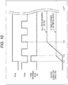
- Fig. 10 is a diagram illustrating the operation of the TDC circuit in Fig. 9 .
- Fig. 10 illustrates, in the order from top, a signal waveform of the reference frequency signal Fref, a signal waveform of the DCO frequency signal Fdco, a signal waveform of the phase difference signal ⁇ F, a Slope of the voltage VF generated in the capacitor 131-1 (C1), and a Slope of the voltage V RAMP generated in the capacitor 131-2 (C2) .
- phase difference signal ⁇ F is provided from the time T11 of a rising edge of the reference frequency signal Fref
- the switch 113-1 is turned on.
- the capacitor 131-1 is charged with current from the current source 161-1, and the voltage VF is generated in the capacitor 131-1.
- the DCO frequency signal Fdco is provided for one period from the time T12 of a rising edge of the DCO frequency signal Fdco immediately thereafter, so that the switch 113-2 is turned on.
- the capacitor 131-2 is charged with current from the current source 161-2, and the voltage V RAMP is generated in the capacitor 131-2.
- the operation of the TDC circuit after the generation of the voltages is basically similar to that of the example of Fig. 8 , and thus the description thereof will be omitted.
- the TDC circuit of Fig. 9 can perform charging of the voltage V F and the voltage V RAMP at the same time without waiting for one period for current charging of the voltage V RAMP , and thus can obtain an AD conversion result faster than the TDC circuit of Fig. 7 .
- Fig. 11 is a circuit diagram illustrating a second modification of the TDC circuit in Fig. 7 .
- the TDC circuit 12 of Fig. 11 differs from the TDC circuit 12 of Fig. 7 in that the capacitances of the capacitors 131-1 and 131-2 are 1 : N, and current sources 181-1 and 181-2 are added instead of the current source 111.
- the rest of the configuration is basically similar to the configuration of Fig. 7 , and thus will not be described.
- Fig. 12 is a diagram illustrating the operation of the TDC circuit in Fig. 11 .
- Fig. 12 illustrates, in the order from top, a signal waveform of the reference frequency signal Fref, a signal waveform of the DCO frequency signal Fdco, a signal waveform of the phase difference signal ⁇ F , a Slope of the voltage VF generated in the capacitor 131-1 (C1), and a Slope of the voltage V RAMP generated in the capacitor 131-2 (C2).
- phase difference signal ⁇ F is provided from the time T21 of a rising edge of the reference frequency signal Fref
- the switch 113-1 is turned on.
- the capacitor 131-1 is charged with current from the current source 181-1, and the voltage VF is generated in the capacitor 131-1.
- the DCO frequency signal Fdco is provided for one period from the time T22 of a rising edge of the DCO frequency signal Fdco immediately thereafter, so that the switch 113-2 is turned on.
- the capacitor 131-2 is charged with current from the current source 181-2, and the voltage V RAMP is generated in the capacitor 131-2.
- the TDC circuit of Fig. 11 can perform charging of the voltage V F and the voltage V RAMP at the same time without waiting for one period for current charging of the voltage V RAMP , and thus can obtain an AD conversion result faster than the TDC circuit of Fig. 7 .
- a time for current charging from a current source can be shortened to improve the intermittent rate, allowing power reduction.
- the phase-locked loop of the present technology is used, for example, in a high-frequency wireless communication device.
- Fig. 13 is a block diagram illustrating a configuration example of a wireless communication device 200 including the ADPLL 1.
- the wireless communication device 200 includes the ADPLL 1, a modulation unit 201, a transmission mixer 202, a reference signal oscillator 203, a reception mixer 204, and a demodulation unit 205.
- the ADPLL 1 outputs a first local signal and a second local signal of a desired frequency to the transmission mixer 202 and the reception mixer 204, respectively, on the basis of a reference signal output from the reference signal oscillator 203.
- the reference signal oscillator 203 is configured using, for example, a crystal oscillator.
- the transmission mixer 202 is provided with a baseband transmission signal modulated by the modulation unit 400 and the first local signal output by the ADPLL 1.
- the transmission mixer 202 up-converts the baseband transmission signal (BB transmission signal) into a high-frequency transmission signal (RF transmission signal) on the basis of the transmission signal and the first local signal provided. Note that the high-frequency transmission signal is transmitted via an antenna not illustrated in Fig. 13 .
- Embodiments of the present technology are not limited to the above-described embodiments, and various modifications can be made without departing from the scope of the present technology.
Landscapes
- Engineering & Computer Science (AREA)
- Theoretical Computer Science (AREA)
- Physics & Mathematics (AREA)
- Nonlinear Science (AREA)
- Stabilization Of Oscillater, Synchronisation, Frequency Synthesizers (AREA)
- Manipulation Of Pulses (AREA)
- Analogue/Digital Conversion (AREA)
Applications Claiming Priority (2)
| Application Number | Priority Date | Filing Date | Title |
|---|---|---|---|
| JP2018037428 | 2018-03-02 | ||
| PCT/JP2019/005554 WO2019167670A1 (fr) | 2018-03-02 | 2019-02-15 | Circuit à boucle à verrouillage de phase |
Publications (2)
| Publication Number | Publication Date |
|---|---|
| EP3761509A1 true EP3761509A1 (fr) | 2021-01-06 |
| EP3761509A4 EP3761509A4 (fr) | 2021-04-14 |
Family
ID=67806097
Family Applications (1)
| Application Number | Title | Priority Date | Filing Date |
|---|---|---|---|
| EP19761589.1A Pending EP3761509A4 (fr) | 2018-03-02 | 2019-02-15 | Circuit à boucle à verrouillage de phase |
Country Status (5)
| Country | Link |
|---|---|
| US (1) | US11115031B2 (fr) |
| EP (1) | EP3761509A4 (fr) |
| JP (1) | JP7346379B2 (fr) |
| CN (1) | CN111771332B (fr) |
| WO (1) | WO2019167670A1 (fr) |
Families Citing this family (2)
| Publication number | Priority date | Publication date | Assignee | Title |
|---|---|---|---|---|
| CN110703246B (zh) * | 2019-10-24 | 2020-11-27 | 中国科学院电子学研究所 | 一种信号同步装置及系统 |
| CN111654281B (zh) * | 2020-06-10 | 2023-08-04 | 上海兆芯集成电路股份有限公司 | 时数转换器 |
Family Cites Families (13)
| Publication number | Priority date | Publication date | Assignee | Title |
|---|---|---|---|---|
| JP3460913B2 (ja) * | 1995-09-29 | 2003-10-27 | 旭化成マイクロシステム株式会社 | 可変遅延時間発生回路とその方法 |
| US5982221A (en) * | 1997-08-13 | 1999-11-09 | Analog Devices, Inc. | Switched current temperature sensor circuit with compounded ΔVBE |
| US6097239A (en) * | 1999-02-10 | 2000-08-01 | Analog Devices, Inc. | Decoupled switched current temperature circuit with compounded ΔV be |
| US7312648B2 (en) * | 2005-06-23 | 2007-12-25 | Himax Technologies, Inc. | Temperature sensor |
| JP5169008B2 (ja) * | 2007-04-27 | 2013-03-27 | 日本電気株式会社 | 電圧制御発振器を内蔵したPLL(PhaseLockedLoop)回路の位相差検出回路 |
| JP5561010B2 (ja) * | 2010-08-09 | 2014-07-30 | 富士通株式会社 | 逐次比較型ad変換器及び逐次比較型ad変換器の動作クロック調整方法 |
| WO2013076797A1 (fr) * | 2011-11-21 | 2013-05-30 | 富士通株式会社 | Adpll |
| US8957712B2 (en) * | 2013-03-15 | 2015-02-17 | Qualcomm Incorporated | Mixed signal TDC with embedded T2V ADC |
| US10177752B2 (en) * | 2014-12-25 | 2019-01-08 | DecaWave, Ltd. | Frequency comparator and early-late detector |
| EP3059857B1 (fr) * | 2015-02-17 | 2021-11-03 | Nxp B.V. | Convertisseur numérique de temps et boucle à verrouillage de phase |
| US9285778B1 (en) * | 2015-08-18 | 2016-03-15 | Cadence Design Systems, Inc. | Time to digital converter with successive approximation architecture |
| EP3139186B1 (fr) * | 2015-09-01 | 2018-08-01 | Nxp B.V. | Circuit de capteur |
| EP3217558B1 (fr) * | 2016-03-11 | 2020-05-13 | Socionext Inc. | Mesure de différence de temps |
-
2019
- 2019-02-15 CN CN201980015277.2A patent/CN111771332B/zh active Active
- 2019-02-15 WO PCT/JP2019/005554 patent/WO2019167670A1/fr not_active Ceased
- 2019-02-15 EP EP19761589.1A patent/EP3761509A4/fr active Pending
- 2019-02-15 US US16/976,670 patent/US11115031B2/en active Active
- 2019-02-15 JP JP2020503392A patent/JP7346379B2/ja active Active
Also Published As
| Publication number | Publication date |
|---|---|
| US20210006255A1 (en) | 2021-01-07 |
| EP3761509A4 (fr) | 2021-04-14 |
| JP7346379B2 (ja) | 2023-09-19 |
| CN111771332A (zh) | 2020-10-13 |
| US11115031B2 (en) | 2021-09-07 |
| WO2019167670A1 (fr) | 2019-09-06 |
| CN111771332B (zh) | 2023-11-21 |
| JPWO2019167670A1 (ja) | 2021-03-04 |
Similar Documents
| Publication | Publication Date | Title |
|---|---|---|
| Pavlovic et al. | A 5.3 GHz digital-to-time-converter-based fractional-N all-digital PLL | |
| US8385476B2 (en) | Digital phase locked loop | |
| US8754713B2 (en) | PLL circuit with improved phase difference detection | |
| KR101797625B1 (ko) | 저전력 고해상도 타임투디지털 컨버터 | |
| JP5347534B2 (ja) | 位相比較器、pll回路、及び位相比較器の制御方法 | |
| US8390347B1 (en) | Single period phase to digital converter | |
| US8432061B2 (en) | Digital frequency divider | |
| US10218364B2 (en) | Time to digital converter, phase difference pulse generator, radio communication device, and radio communication method | |
| US9748961B2 (en) | Single cycle asynchronous domain crossing circuit for bus data | |
| KR102123901B1 (ko) | 완전 디지털 위상 고정 루프 회로, 반도체 장치 및 휴대 정보 기기 | |
| CN107026647B (zh) | 时间数字系统以及频率合成器 | |
| EP3758233B1 (fr) | Synchronisation d'horloge dans une adpll | |
| JP2017229024A (ja) | 位相デジタル変換器、無線通信装置および無線通信方法 | |
| US11115031B2 (en) | Phase-locked loop | |
| US20110133795A1 (en) | Digital phase-locked loop with reduced loop delay | |
| JP2012075000A (ja) | 位相同期回路及び無線機 | |
| Lin et al. | A 2.4-GHz 500-µW 370-fs rms Integrated Jitter Sub-Sampling Sub-Harmonically Injection-Locked PLL in 90-nm CMOS | |
| JP2013077869A (ja) | 時間−デジタル変換器及びpll回路 | |
| EP3624344B1 (fr) | Circuit pll | |
| US11916568B2 (en) | Sampling circuit with a hierarchical time step generator | |
| JP2010273185A (ja) | デジタルフェーズロックドループ回路 | |
| Huang et al. | A time-to-digital converter based AFC for wideband frequency synthesizer | |
| Govindaraj et al. | Dtc-assisted all-digital phase-locked loop exploiting hybrid time/voltage phase digitization | |
| Badal et al. | High-resolution time to digital converter in 0.13 µm CMOS process for RFID phase locked loop | |
| Hong | A 0.012 mm2 and 2.5 mW bang–bang digital PLL using pseudo random number generator |
Legal Events
| Date | Code | Title | Description |
|---|---|---|---|
| STAA | Information on the status of an ep patent application or granted ep patent |
Free format text: STATUS: THE INTERNATIONAL PUBLICATION HAS BEEN MADE |
|
| PUAI | Public reference made under article 153(3) epc to a published international application that has entered the european phase |
Free format text: ORIGINAL CODE: 0009012 |
|
| STAA | Information on the status of an ep patent application or granted ep patent |
Free format text: STATUS: REQUEST FOR EXAMINATION WAS MADE |
|
| 17P | Request for examination filed |
Effective date: 20200922 |
|
| AK | Designated contracting states |
Kind code of ref document: A1 Designated state(s): AL AT BE BG CH CY CZ DE DK EE ES FI FR GB GR HR HU IE IS IT LI LT LU LV MC MK MT NL NO PL PT RO RS SE SI SK SM TR |
|
| AX | Request for extension of the european patent |
Extension state: BA ME |
|
| REG | Reference to a national code |
Ref country code: DE Ref legal event code: R079 Free format text: PREVIOUS MAIN CLASS: H03K0005260000 Ipc: H03L0007091000 |
|
| A4 | Supplementary search report drawn up and despatched |
Effective date: 20210316 |
|
| RIC1 | Information provided on ipc code assigned before grant |
Ipc: H03L 7/091 20060101AFI20210310BHEP Ipc: H03L 7/085 20060101ALI20210310BHEP Ipc: H03M 3/00 20060101ALI20210310BHEP Ipc: H03K 5/26 20060101ALI20210310BHEP |
|
| DAV | Request for validation of the european patent (deleted) | ||
| DAX | Request for extension of the european patent (deleted) | ||
| STAA | Information on the status of an ep patent application or granted ep patent |
Free format text: STATUS: EXAMINATION IS IN PROGRESS |
|
| 17Q | First examination report despatched |
Effective date: 20230202 |
|
| GRAP | Despatch of communication of intention to grant a patent |
Free format text: ORIGINAL CODE: EPIDOSNIGR1 |
|
| STAA | Information on the status of an ep patent application or granted ep patent |
Free format text: STATUS: GRANT OF PATENT IS INTENDED |
|
| INTG | Intention to grant announced |
Effective date: 20241030 |
|
| GRAJ | Information related to disapproval of communication of intention to grant by the applicant or resumption of examination proceedings by the epo deleted |
Free format text: ORIGINAL CODE: EPIDOSDIGR1 |
|
| STAA | Information on the status of an ep patent application or granted ep patent |
Free format text: STATUS: EXAMINATION IS IN PROGRESS |
|
| INTC | Intention to grant announced (deleted) |