EP3762995B1 - Oberflächenmontierbarer dünnschicht-hochfrequenzkoppler - Google Patents
Oberflächenmontierbarer dünnschicht-hochfrequenzkoppler Download PDFInfo
- Publication number
- EP3762995B1 EP3762995B1 EP19765102.9A EP19765102A EP3762995B1 EP 3762995 B1 EP3762995 B1 EP 3762995B1 EP 19765102 A EP19765102 A EP 19765102A EP 3762995 B1 EP3762995 B1 EP 3762995B1
- Authority
- EP
- European Patent Office
- Prior art keywords
- thin film
- coupler
- base substrate
- microstrip
- ground plane
- Prior art date
- Legal status (The legal status is an assumption and is not a legal conclusion. Google has not performed a legal analysis and makes no representation as to the accuracy of the status listed.)
- Active
Links
Images




Classifications
-
- H—ELECTRICITY
- H01—ELECTRIC ELEMENTS
- H01P—WAVEGUIDES; RESONATORS, LINES, OR OTHER DEVICES OF THE WAVEGUIDE TYPE
- H01P11/00—Apparatus or processes specially adapted for manufacturing waveguides or resonators, lines, or other devices of the waveguide type
-
- H—ELECTRICITY
- H01—ELECTRIC ELEMENTS
- H01P—WAVEGUIDES; RESONATORS, LINES, OR OTHER DEVICES OF THE WAVEGUIDE TYPE
- H01P11/00—Apparatus or processes specially adapted for manufacturing waveguides or resonators, lines, or other devices of the waveguide type
- H01P11/001—Manufacturing waveguides or transmission lines of the waveguide type
- H01P11/003—Manufacturing lines with conductors on a substrate, e.g. strip lines, slot lines
-
- H—ELECTRICITY
- H01—ELECTRIC ELEMENTS
- H01P—WAVEGUIDES; RESONATORS, LINES, OR OTHER DEVICES OF THE WAVEGUIDE TYPE
- H01P3/00—Waveguides; Transmission lines of the waveguide type
- H01P3/003—Coplanar lines
-
- H—ELECTRICITY
- H01—ELECTRIC ELEMENTS
- H01P—WAVEGUIDES; RESONATORS, LINES, OR OTHER DEVICES OF THE WAVEGUIDE TYPE
- H01P3/00—Waveguides; Transmission lines of the waveguide type
- H01P3/02—Waveguides; Transmission lines of the waveguide type with two longitudinal conductors
- H01P3/08—Microstrips; Strip lines
- H01P3/081—Microstriplines
-
- H—ELECTRICITY
- H01—ELECTRIC ELEMENTS
- H01P—WAVEGUIDES; RESONATORS, LINES, OR OTHER DEVICES OF THE WAVEGUIDE TYPE
- H01P3/00—Waveguides; Transmission lines of the waveguide type
- H01P3/18—Waveguides; Transmission lines of the waveguide type built-up from several layers to increase operating surface, i.e. alternately conductive and dielectric layers
-
- H—ELECTRICITY
- H01—ELECTRIC ELEMENTS
- H01P—WAVEGUIDES; RESONATORS, LINES, OR OTHER DEVICES OF THE WAVEGUIDE TYPE
- H01P5/00—Coupling devices of the waveguide type
- H01P5/12—Coupling devices having more than two ports
-
- H—ELECTRICITY
- H01—ELECTRIC ELEMENTS
- H01P—WAVEGUIDES; RESONATORS, LINES, OR OTHER DEVICES OF THE WAVEGUIDE TYPE
- H01P5/00—Coupling devices of the waveguide type
- H01P5/12—Coupling devices having more than two ports
- H01P5/16—Conjugate devices, i.e. devices having at least one port decoupled from one other port
- H01P5/18—Conjugate devices, i.e. devices having at least one port decoupled from one other port consisting of two coupled guides, e.g. directional couplers
- H01P5/184—Conjugate devices, i.e. devices having at least one port decoupled from one other port consisting of two coupled guides, e.g. directional couplers the guides being strip lines or microstrips
- H01P5/185—Edge coupled lines
-
- H—ELECTRICITY
- H05—ELECTRIC TECHNIQUES NOT OTHERWISE PROVIDED FOR
- H05K—PRINTED CIRCUITS; CASINGS OR CONSTRUCTIONAL DETAILS OF ELECTRIC APPARATUS; MANUFACTURE OF ASSEMBLAGES OF ELECTRICAL COMPONENTS
- H05K1/00—Printed circuits
- H05K1/02—Details
- H05K1/0213—Electrical arrangements not otherwise provided for
- H05K1/0237—High frequency adaptations
-
- H—ELECTRICITY
- H05—ELECTRIC TECHNIQUES NOT OTHERWISE PROVIDED FOR
- H05K—PRINTED CIRCUITS; CASINGS OR CONSTRUCTIONAL DETAILS OF ELECTRIC APPARATUS; MANUFACTURE OF ASSEMBLAGES OF ELECTRICAL COMPONENTS
- H05K1/00—Printed circuits
- H05K1/02—Details
- H05K1/11—Printed elements for providing electric connections to or between printed circuits
- H05K1/115—Via connections; Lands around holes or via connections
-
- H—ELECTRICITY
- H04—ELECTRIC COMMUNICATION TECHNIQUE
- H04W—WIRELESS COMMUNICATION NETWORKS
- H04W88/00—Devices specially adapted for wireless communication networks, e.g. terminals, base stations or access point devices
- H04W88/08—Access point devices
-
- H—ELECTRICITY
- H05—ELECTRIC TECHNIQUES NOT OTHERWISE PROVIDED FOR
- H05K—PRINTED CIRCUITS; CASINGS OR CONSTRUCTIONAL DETAILS OF ELECTRIC APPARATUS; MANUFACTURE OF ASSEMBLAGES OF ELECTRICAL COMPONENTS
- H05K2201/00—Indexing scheme relating to printed circuits covered by H05K1/00
- H05K2201/10—Details of components or other objects attached to or integrated in a printed circuit board
- H05K2201/10007—Types of components
- H05K2201/10098—Components for radio transmission, e.g. radio frequency identification [RFID] tag, printed or non-printed antennas
Definitions
- High frequency radio signal communication has increased in popularity.
- the demand for increased data transmission speed for wireless smartphone connectivity has driven demand for high frequency components, including those configured to operate at 5G spectrum frequencies.
- a trend towards miniaturization has also increased the desirability of small, passive components for handling such high frequency signals.
- Miniaturization has also increased the difficulty of surface mounting small, passive components suitable for operation in the 5G frequency spectrum.
- a compact, high frequency coupler that is easily surface mounted would be welcomed in the art. Surface mountable couplers of the prior art are disclosed in US 5802688 A and JPH 0837347 A .
- a high frequency, surface mountable coupler as defined in claim 1, is disclosed.
- the coupler includes a monolithic base substrate having a top surface, a bottom surface, a length in a longitudinal direction, and a width in a lateral direction that is perpendicular to the longitudinal direction.
- the coupler includes a first thin film microstrip disposed on the top surface of the monolithic base substrate.
- the first microstrip has an input end and an output end.
- the coupler includes a second thin film microstrip disposed on the top surface of the monolithic base substrate.
- the second microstrip has an input end and an output end.
- the coupler includes at least one via extending through the monolithic base substrate from the top surface to the bottom surface of the monolithic base substrate.
- the via(s) are electrically connected with at least one of the input end or the output end of the first microstrip or the second microstrip.
- the coupler has a coupling factor that is greater than about -30 dB at about 28 GHz.
- a method for forming a high frequency, surface mountable coupler as defined in claim 7, is disclosed.
- the method includes forming at least one via through hole that extends from a top surface of a monolithic base substrate to a bottom surface of the monolithic base substrate.
- the method includes depositing each of a first thin film microstrip and a second thin film microstrip on the top surface of the monolithic base substrate.
- Each of the first and second thin film microstrips are sized and spaced apart such that the coupler has a coupling factor that is greater than about -30 dB at about 28 GHz.
- the method includes depositing a conductive via material inside the via through hole(s) to form at least one via electrically connecting at least one of the first thin film microstrip or the second thin film microstrip with a contact pad on the bottom surface of the monolithic base substrate.
- a base station circuit in accordance with another aspect of the present invention, includes a signal source component and a high frequency, surface mountable coupler according to claim 1 operatively connected with the signal source component.
- the coupler includes a monolithic base substrate having a top surface, a bottom surface, a length in a longitudinal direction, and a width in a lateral direction that is perpendicular to the longitudinal direction.
- the coupler includes a first thin film microstrip disposed on the top surface of the monolithic base substrate. The first microstrip having an input end and an output end.
- the coupler includes a second thin film microstrip disposed on the top surface of the monolithic base substrate. The second microstrip has an input end and an output end.
- At least one via extends through the monolithic base substrate from the top surface to the bottom surface of the monolithic base substrate.
- the via(s) are electrically connected with at least one of the input end or the output end of the first microstrip or the second microstrip.
- the coupler has a coupling factor that is greater than about -30 dB at about 28 GHz.
- a surface mountable coupler device is provided that is particularly useful in high frequency circuits, including those operating in the 5G frequency spectrum.
- the 5G frequency spectrum generally extends from about 20 GHz to about 30 GHz.
- Couplers generally provide coupling between two signal lines without direct electrical contact. Exemplary uses include radio frequency (RF) mixers, amplifiers, and modulators. For instance, couplers may be used to provide coupling for a feedback control loop or an amplifier output section in a RF transmitter.
- RF radio frequency
- a thin film coupler may be formed on one or more monolithic substrates.
- the thin film coupler may include a base substrate and a cover substrate.
- the substrate(s) may comprise one or more suitable ceramic materials. Suitable materials are generally electrically insulating and thermally conductive.
- the substrate may comprise alumina (Al 2 O 3 ), aluminum nitride (AIN), beryllium oxide (BeO), aluminum oxide (Al 2 O 3 ), boron nitride (BN), silicon (Si), silicon carbide (SiC), silica (SiO 2 ), silicon nitride (Si 3 N 4 ), gallium arsenide (GaAs), gallium nitride (GaN), zirconium dioxide (ZrO 2 ), mixtures thereof, oxides and/or nitrides of such materials, or any other suitable ceramic material.
- Additional ceramic materials include barium titanate (BaTiO 3 ), calcium titanate (CaTiO 3 ), zinc oxide (ZnO), ceramics containing low-fire glass, and other glass-bonded materials.
- one or more of the substrates may comprise sapphire or ruby.
- Sapphire and ruby are types of corundum, which is a crystalline form of aluminum oxide (a ceramic material) containing additional trace materials.
- a substrate comprising sapphire may provide several benefits including excellent electrical insulation, heat dissipation, and high temperature stability. Additionally, because sapphire is generally transparent, internal features of the coupler may be visually inspected, reducing the time and difficulty associated with checking completed components for quality.
- the coupler may include various thin film components, including a pair of microstrips formed on a top surface of the base substrate and a base ground plane formed on a bottom surface of the base substrate.
- the coupler may also include an additional thin film ground plane disposed on a top surface of the cover substrate.
- the cover substrate may be arranged on the top surface of the base substrate.
- the thin film components may have thicknesses of about 50 micrometers or less, in some embodiments 20 micrometers or less, and in some embodiments 5 micrometers or less.
- the thickness of the thin film components may range from about 0.05 micrometers to about 50 micrometers, in some embodiments from about 0.1 micrometers to about 20 micrometers, in some embodiments from about 1 micrometer to about 5 micrometers, e.g., about 3 micrometers.
- the thin film components may be precisely formed using a variety of suitable subtractive, semi-additive, or fully additive processes.
- physical vapor deposition and/or chemical deposition may be used.
- the thin film components may be formed using sputtering, a type of physical vapor deposition.
- a variety of other suitable processes may be used, however, including plasma-enhanced chemical vapor deposition (PECVD) and electroless plating, for example.
- PECVD plasma-enhanced chemical vapor deposition
- Lithography masks and etching may be used to produce the desired shape of the thin film components.
- suitable etching techniques may be used including dry etching using a plasma of a reactive gas (e.g., oxygen, chlorine, boron trichloride) and/or wet etching.
- a reactive gas e.g., oxygen, chlorine, boron trichloride
- the thin film components may be formed from a variety of suitable electrically conductive materials.
- Example materials include copper, nickel, gold, tin, lead, palladium, silver, and alloys thereof. Any conductive metallic or non-metallic material that is suitable for thin film fabrication may be used, however.
- Vias may connect the microstrips on the top surface of the base substrate with contact pads on the bottom surface of the base substrate. This may allow the thin film coupler to be surface mounted to a printed circuit board (PCB), for example.
- the vias may be formed by laser drilling holes through the base substrate and then filling (e.g., sputtering, electroless plating) the internal surfaces of the holes with a suitable conductive material.
- the through holes for the vias may be filled concurrently with the performance of another manufacturing step. For example, the vias may be drilled before the thin film components are formed such that both the vias and the thin film components may be simultaneously deposited.
- the vias may be formed from a variety of suitable materials including those described above with reference to the thin film components (e.g., microstrips and ground plane).
- one or more protective layers may be exposed along an exterior of the coupler.
- the protective layer(s) may be formed over a top surface and/or a bottom surface of the coupler.
- formed over may refer to a layer that is directly in contact with another layer. However, intermediate layers may also be formed therebetween. Additionally, when used in reference to a bottom surface, “formed over” may be used relative to an exterior surface of the component. Thus, a layer that is "formed over" a bottom surface may be closer to the exterior of the component than the layer over which it is formed.
- a top protective layer may be formed over the top surface of base substrate and microstrips or over a top surface of the cover substrate (if present).
- a bottom protective layer may be exposed along a bottom surface of the coupler, for example formed over the bottom surface of the base substrate.
- the bottom protective layer may be formed using photolithography techniques in a manner that leaves openings or windows through which the contact pads may be deposited, for example by electroplating.
- the protective layer(s) may include a polymeric material, such as polyimide, SiNO, Al2O3, SiO2, Si3N4, benzocyclobutene, or glass.
- the protective layer may have a thickness that ranges from about 1 micron to about 300 microns.
- the thin film coupler may be configured to be surface mounted on a base surface, such as printed circuit board (PCB), such that the bottom surface of the base substrate is connected with the PCB.
- the thin film coupler may be configured for grid array-type surface mounting.
- the thin film coupler may be configured for land grid array (LGA) type mounting, ball grid array (BGA) type mounting, or any other suitable type of grid array-type surface mounting.
- LGA land grid array
- BGA ball grid array
- a high frequency coupler can be achieved that has a coupling factor that is greater than about -30 dB at about 28 GHz and that is suitable for grid array mounting.
- the coupling factor may be greater than about -25 dB at about 28 GHz, and in some embodiments greater than about -20 dB at about 28 GHz, e.g., -19.9 dB.
- the coupler may also be suitable for coupling across a broad range of high frequencies.
- coupler may have a coupling factor that is greater than about -35 dB from about 18 GHz to about 32 GHz, or higher, in some embodiments, greater than about -30 dB from about 18 GHz to about 32 GHz, and in some embodiments greater than about -25 dB from about 18 GHz to about 32 GHz.
- the coupler may have a coupling factor that is greater than about -35 dB from about 10 GHz to about 70 GHz, in some embodiments, greater than about -30 dB from about 10 GHz to about 70 GHz, and in some embodiments greater than about -25 dB from about 10 GHz to about 70 GHz.
- coupler may have a low return loss, which is desirable because return loss represents the portion of the signal that is reflected back by the coupler.
- the return loss may be less than -15 dB from about 10 GHz to about 70 GHz, in some embodiments less than about -20 dB from about 20 GHz to about 32 GHz, in some embodiments less than about -25 dB from about 21 GHz to about 32 GHz, and in some embodiments less than about -30 dB from about 22 GHz to about 32 GHz.
- the return loss may be less than about -35 dB at about 28 GHz.
- the coupler may have an insertion loss that is near zero, which indicates that the signal is passed through a transmission line of the coupler without being substantially affected.
- the insertion loss may be greater than about -1 dB from about 18 GHz to about 32 GHz, in some embodiments greater than about -0.75 dB from about 18 GHz to about 32 GHz, and in some embodiments greater than about -0.6 dB from about 18 GHz to about 32 GHz.
- the insertion loss may be greater than about -1 dB from about 10 GHz to about 70 GHz, in some embodiments greater than about -0.75 dB from about 10 GHz to about 70 GHz, and in some embodiments greater than about -0.6 dB from about 10 GHz to about 70 GHz.
- the coupler may also have an isolation factor that is less than about -25 dB from about 18 GHz to about 32 GHz, in some embodiments less than about -30 dB from about 18 GHz to about 32 GHz. Additionally, in some embodiments, the coupler may have an isolation factor that is less than about -25 dB from about 10 GHz to about 70 GHz, in some embodiments less than about -30 dB from about 10 GHz to about 70 GHz. In some embodiments, the isolation factor may be less than about -35 dB at about 28 GHz, in some embodiments less than about -40 dB at about 28 GHz, in some embodiments less than about -45 dB at about 28 GHz.
- the coupler includes a pair of microstrips disposed on a top surface of a base substrate. At least a portion of the microstrips may be arranged substantially parallel to each other along a coupling length.
- the coupling length may be selected to obtain the desired performance characteristics of the coupler, including the coupling factor.
- the performance characteristics of the coupler may generally be optimized when the coupling length is equal to or proportional to (e.g., a multiple of) ⁇ /4, where ⁇ is wavelength of a desired operating frequency of the coupler propagating through the base substrate and/or cover substrate.
- a coupling length of the microstrips may be equal to or proportional to ⁇ /4.
- the length(s) of the via(s) may be equal to or proportional to ⁇ /4.
- the dielectric constant of the base substrate material and/or cover substrate material may range from about 0.1 to about 50 as determined in accordance with ASTM D2520-13 at an operating temperature of 25°C and frequency of 28 GHz, in some embodiments from about 0.5 to about 20, in some embodiments from about 1 to about 20, and in some embodiments from about 5 to about 15, e.g., about 9.
- the coupling length ranges from about 0.1 mm to about 3.8 mm, in some embodiments from about 0.2 mm to about 3 mm, in some embodiments from about 0.3 mm to about 2.8 mm, and in some embodiments from about 0.3 mm to about 1.5 mm.
- the coupling length may be approximately equal to 0.9 mm, corresponding to ⁇ /4 for about 28 GHz and a dielectric material having a dielectric constant of about 9 as determined in accordance with ASTM D2520-13 at an operating temperature of 25°C and frequency of 28 GHz.
- the parallel portions of the microstrips may be spaced apart by a gap distance.
- the gap distance may be selected to obtain the desired performance characteristics of the coupler e.g., (desired impedance) and the specific component materials implemented.
- the gap distance may range from about 50 micrometers ( ⁇ m) to about 750 ⁇ m, in some embodiments from about 100 ⁇ m to about 700 ⁇ m, in some embodiments from about 300 ⁇ m to about 600 ⁇ m, e.g., 200 ⁇ m.
- the microstrips may also have a width ranging from about 50 ⁇ m to about 500 ⁇ m, in some embodiments from about 100 ⁇ m to about 400 ⁇ m, in some embodiments from about 200 ⁇ m to about 300 ⁇ m, e.g., about 250 ⁇ m.
- the micostrips are shielded by one or more ground planes.
- the ground plane(s) e.g., base ground plane and/or cover ground plane
- the thicknesses of the substrates may range from about 50 ⁇ m to about 500 ⁇ m, in some embodiments from about 100 ⁇ m to about 400 ⁇ m, in some embodiments from about 200 ⁇ m to about 300 ⁇ m, e.g., about 250 ⁇ m. In some embodiments, the thicknesses of the substrate(s) may be selected to be approximately equal to the width of the microstrips.
- the vias may also be configured to contribute to the excellent coupling characteristics of the coupler.
- the vias connect respective ends of the microstrips (on the top surface of the base substrate) with respective contact pads (on the bottom surface of the base substrate).
- the at least one via (114) comprises a first via (114) electrically connecting the input end of the first thin film microstrip (104) to a first of the four contact pads (116), a second via (114) electrically connecting the output end of the first thin film microstrip (104) to a second of the four contact pads (116), a third via (114) electrically connecting the input end of the second thin film microstrip (104) to a third of the four contact pads (116), and a fourth via (114) electrically connecting the output end of the second thin film microstrip (104) to a fourth of the four contact pads (116).
- the vias are formed through the base substrate.
- the lengths of the vias may be equal to the thickness of the base substrate.
- the lengths of the vias may be selected to be equal or proportional to ⁇ /4, which may contribute to the excellent coupling characteristics of the coupler.
- the coupler may include at least one adhesion layer in contact with the thin-film microstrips.
- the adhesion layer may be or include a variety of materials that are suitable for improving adhesion between the thin-film microstrips and adjacent layers, such as the base substrate, cover substrate, and/or protective layer (e.g., polymeric layer).
- the adhesion layer may include at least one of Ta, Cr, TaN, TiW, Ti, or TiN.
- the adhesive layer may be or include tantalum (Ta) (e.g., tantalum or an oxide or nitride thereof).
- Ta tantalum
- the material of the adhesion layer may be selected to overcome phenomena such as lattice mismatch and residual stresses.
- the adhesion layer(s) may have a variety of suitable thicknesses.
- the thicknesses of the adhesion layer(s) may range from about 100 angstroms to about 1000 angstroms, in some embodiments from about 200 angstroms to about 800 angstroms, in some embodiments from about 400 angstroms to about 600 angstroms.
- the coupler may have a compact form.
- each of a length and a width of the coupler may be less than about 5.0 mm, in some embodiments less than about 3.5 mm, and in some embodiments less than about 2.5 mm.
- each of the length and width of the coupler may range from about 0.5 mm to about 5 mm, in some embodiments from about 1 mm to about 4 mm, and in some embodiments from about 2.5 mm to about 3.5 mm.
- the coupler may be configured for grid array type mounting.
- vias may facilitate grid array type mounting of the coupler to a PCB.
- Exemplary types of grid array mounting include ball grid array and land grid array.
- the vias may be electrically connected with respective contact pads disposed on a bottom surface of the coupler.
- a base ground plane may also be disposed on the bottom surface of the coupler. The contact pads and base ground plane may provide electrical connections on the bottom surface of the base substrate such that the coupler may be surface mounted using grid array type mounting.
- Grid array type mounting may provide significant advantages. For example, mounting the coupler to a PCB may be performed more efficiently, reducing assembly cost. Additionally, manufacturing costs associated with forming the high frequency surface mountable coupler may be reduced compared with alternative mounting options.
- the described configuration may also protect electrical contacts (e.g., contact pads and base ground plane) from electrically shorting because all electrical contacts may be obscured and protected underneath the coupler or underneath the cover substrate. Additionally, the base ground plane may provide for attachment along a significant portion of the total area of the coupler. This may result in a more robust physical connection between the coupler and the PCB.
- FIG. 1A illustrates a top down view of one embodiment of a thin film coupler 100 in accordance with aspects of the present disclosure.
- FIG. 1B illustrates a cross section view along section A-A in FIG. 1A .
- the thin film coupler 100 includes a base substrate 102 and a pair of microstrips 104.
- the base substrate has a top surface 106, and the microstrips 104 are formed on the top surface 106 of the base substrate 102.
- the base substrate 102 also has a length (represented by L s in FIG. 1A ) in a longitudinal direction 103, and a width (represented by W s in FIG. 1A ) in a lateral direction 105 that is perpendicular to the longitudinal direction 103.
- the base substrate 102 may also have a thickness (represented by T s in FIG. 1A ) in a Z direction 107 that is perpendicular to each of the longitudinal direction 103 and the lateral direction 105.
- One of the microstrips 104 may function as a transmission line, and the other of the microstrips 104 may function as a coupled line. At least a portion of the microstrips 104 is arranged substantially parallel to each other along a coupling length (represented by L c in FIG. 1A ). In some embodiments, the coupling length, L c , may be proportional to ⁇ /4, where ⁇ represents the desired operating frequency of the coupler.
- the microstrips 104 may also have a width (represented by W m in FIG. 1A ). The microstrips 104 may be arranged such that a gap (represented by G m in FIG. 1A ) is formed between the microstrips 104. The electromagnetic interaction between the microstrips 104 may cause a signal through one of the microstrips 104 (the transmission line) to induce a signal in the other of the microstrips 104 (the coupled line).
- a cover substrate 108 may overlay each of the top surface 106 of the base substrate 102 and the microstrips 104 that are formed on the top surface 106.
- the cover substrate 108 is omitted from FIG. 1A for clarity such that the top surface 106 of the base substrate 102 is visible.
- the cover substrate 108 is visible in FIG. 1B , however.
- the cover substrate 108 may protect the microstrips 104 from electrical short by contact with other electrically conductive objects.
- the cover substrate 108 may further protect the microstrips 104 from damage by abrasion or impact. Additionally, the cover substrate 108 may provide a suitable location for marking the coupler 100, including, for example, performance specifications / characteristics, port labels, etc.
- Vias 114 are formed through the base substrate 102 from the top surface 106 to the bottom surface 110.
- the vias 114 electrically connect respective ends of the pair of microstrips 104 with contact pads 116 formed on the bottom surface 110 of the base substrate 102.
- Each microstrip 104 has an input end and an output end that is electrically connected with a respective via 114.
- the vias 114 electrically connect the input end or output end of one of the microstrips 104 to respective contact pads 116 such that the contact pads 116 act as electrical ports for the coupler 100.
- the contact pads 116 may be configured for grid array mounting.
- a conductive material may be disposed on the contacts pads 116 for land grid array or ball grid array type surface mounting.
- the conductive material may comprise copper, nickel, aluminum, palladium, gold, silver, platinum, lead, tin, alloys of these materials, or any other suitable conductive substance suitable as a solder material.
- the coupler 100 may be arranged in the desired location and heated such that the solder melts forming electrical connections with the mounting surface (e.g., PCB).
- a base ground plane 112 is formed on the bottom surface 110 of the base substrate 102. As such, the base ground plane 112 may be spaced apart from the microstrips 104 by the thickness (represented by T s in FIG. 1A ) of the base substrate 102. The base ground plane 112 may be generally parallel with the microstrips 104. The thickness of the base substrate 102 may be selected to produce the desired shielding effect on the microstrips 104 and/or selected to produce the desired response characteristics of the coupler 100.
- the base ground plane 112 is located between the vias 114 in the longitudinal direction 103 (or lateral direction 105) such that the contact pads 116 are adjacent to corners of the base ground plane 112. Additionally, in some embodiments, the base ground plane 112 may extend substantially all of the length or width of the base substrate 102. The base ground plane 112 is sized such that the ground plane 112 can extend between contact pads 116 without directly contacting the contact pads 116. For example, in some embodiments, the ground plane 112 may extend substantially to an edge of the bottom surface 110 of the base substrate 102. This may provide a larger surface by which the coupler 100 can be surface mounted, thereby providing a more mechanically robust attachment.
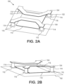
- FIGS. 2A and 2B illustrate perspective views of the embodiment of the thin film coupler described above with reference to FIGS. 1A and 1B .
- the cover substrate 108 is omitted for clarity. Only the bottom surface of the base substrate 102 is shown for clarity.
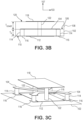
- FIG. 3A illustrates a top down view of another embodiment of a thin film coupler 100 including a cover ground plane 118, according to aspects of the present disclosure.
- the cover substrate 108 is omitted for clarity.
- FIG 3B illustrates a section view along section A-A in FIG. 3A .
- FIG. 3C illustrates a perspective view in which the cover substrate 108 is omitted for clarity. Only the bottom surface 110 of the base substrate 102 is shown.
- the coupler 100 may generally be configured as described above with reference to FIGS. 1A, 1B , 2A, and 2B .
- the coupler 100 may include the cover ground plane 118, which may be formed on the top surface 120 of the cover substrate 108.
- the cover substrate 108 may have a thickness (represented in FIG. 3B as T cover ) in the Z direction 107.
- the cover ground plane 118 may be spaced apart from the microstrips 104 in the Z direction 107 by the thickness of the cover substrate 108.
- the cover ground plane 118 may be generally parallel with the microstrips 104 and/or the base ground plane 112.
- the thickness of the cover substrate 108 may be selected to produce the desired shielding effect on the microstrips 104 and/or selected to produce the desired response characteristics of the coupler 100.
- the cover ground plane 118 may be electrically connected with the base ground plane 112 in a variety of ways.
- one or more ground vias 122 may extend through the base substrate 102 and the cover substrate 108 and electrically connect the cover ground plane 118 with the base ground plane 112.
- a pair of ground vias 122 may be symmetrically arranged on either side of the microstrips 104.
- a single ground via 122 may electrically connect the cover ground plane 118 with the base ground plane 112.
- the cover ground plane 118 may be electrically connected through a side wall connection, castellation type connection, or any other suitable type of electrical connection to the base ground plane 112 and/or the bottom surface 110 of the base substrate 102.
- a side wall connection may be formed that extends from the cover ground plane 118 to the base ground plane 112 or the bottom surface 110 of the base substrate 102.
- the side wall connection may be formed by sputtering or any other suitable deposition technique on a surface of the base substrate 102 and/or cover substrate 108 that extends in the Z direction 107.
- a castellation type connection may be formed by drilling holes in the substrates 102, 108 along dicing lines before the substrates 102, 108 are diced along the dicing lines to form individual couplers 100.
- a conductive layer may be formed on the resulting castellation surface using sputtering or any other suitable deposition technique.
- the cover ground plane 112 may provide several advantages. For example, the cover ground plane 112 may provide additional electromagnetic shielding of the microstrips 104. This may reduce the amount of electromagnetic interference from ambient radio waves, for example.
- the coupler may be partially configured for grid array-type mounting.
- a single via or a pair of vias may connect one or two ends of the microstrips with respective contact pads on the bottom surface of the base substrate.
- the other ends of the microstrips may be electrically connected using any other suitable means, including conductive castellations, soldered wires, etc.
- FIG. 4 illustrates diagrammatic views of various surfaces of several embodiments of the coupler in accordance with aspects of the present disclosure.
- the shaded portions of "PAD1” represent thin film layers on the bottom surface of the base substrate that form the base ground plane and contact pads.
- the shaded portions of “PAD2” represent thin film layers on the top surface of the base substrate that form the microstrips.
- VIP illustrates the locations of the vias in the base substrate.
- the shaded portions of "LGA” illustrate the shapes of a layer of conductive material formed over the base ground plane and contact pads to facilitate land grid array-type surface mounting of the coupler.
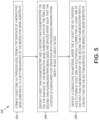
- aspects of the present disclosure are directed to a method 200 for making a high frequency coupler configured for array type surface mounting.
- the method 200 will be described herein with reference to the thin film coupler 100 described above with reference to FIGS. 1-3 .
- the disclosed method 200 may be implemented with any suitable thin film coupler.
- FIG. 5 depicts steps performed in a particular order for purposes of illustration and discussion, the methods discussed herein are not limited to any particular order or arrangement.
- steps of the methods disclosed herein can be omitted, rearranged, combined, and/or adapted in various ways without deviating from the scope of the present disclosure.
- the method 200 includes, at (202), forming at least one via through hole that extends from a top surface of a monolithic base substrate to a bottom surface of the monolithic base substrate.
- the through hole(s) may be formed using laser drilling or any other suitable method.
- multiple couplers may be formed on a base substrate sheet, which may be diced to form individual couplers.
- the method includes, at (204), depositing a first thin film microstrip and a second thin film microstrip on a top surface of a monolithic base substrate.
- an additive technique e.g., sputtering, electroless plating, etc.
- a lithographic screen may be deposited over the conductive metal layer. Portions of the copper layer may then be removed using any suitable etching technique to produce the desired pattern for the microstrips.
- a second etching step may then be used to remove the lithographic screen.
- suitable etching techniques may be used, including dry etching using a plasma of a reactive gas (e.g., oxygen, chlorine, boron trichloride).
- Each of the first and second thin film microstrips may be sized and spaced apart to provide the desired performance characteristics.
- the coupler may have a coupling factor that is greater than about -30 dB from about 18 GHz to about 32 GHz.
- the coupler has a coupling factor that is greater than about -30 dB at about 28 GHz.
- the coupling length (represented by L c in FIG. 1A ) along which the microstrips are substantially parallel to each other may be sized to produce the desired characteristics. For example, in some embodiments, this length may be equal to about ⁇ /4 or ⁇ /8, where ⁇ represents the desired operating frequency of the coupler (e.g., 28 GHz), as discussed above.
- the method includes, at (206), depositing a conductive via material inside the at least one via through hole to form at least one via electrically connecting at least one of the first thin film microstrip or the second thin film microstrip with a contact pad on the bottom surface of the monolithic base substrate.
- the at least one via (114) comprises a first via (114) electrically connecting the input end of the first thin film microstrip (104) to a first of the four contact pads (116), a second via (114) electrically connecting the output end of the first thin film microstrip (104) to a second of the four contact pads (116), a third via (114) electrically connecting the input end of the second thin film microstrip (104) to a third of the four contact pads (116), and a fourth via (114) electrically connecting the output end of the second thin film microstrip (104) to a fourth of the four contact pads (116).
- depositing the conductive via material may include sputtering, electroless plating, or any other suitable thin film deposition process. In some embodiments, this may be performed concurrently with the deposition of the microstrips, at (204).
- the method 200 also includes forming a base ground plane on a bottom surface of the monolithic base substrate.
- the base ground plane may be formed in a similar manner as described above regarding forming the microstrips, at (204).
- the base ground plane may be formed during the same thin film formation steps (e.g., deposition, lithography, etching) described above that may be used to form the microstrips, at (204).
- the method 200 may also include forming a layer of conductive material (e.g., solder, tin, lead, gold, alloys thereof or any other suitable conductive material) over the base ground plane and/or contact pads on the bottom surface of the monolithic base substrate that is suitable for grid array-type mounting.
- FIG. 6A illustrates a diagrammatic view of an embodiment of a coupler 300 having a transmission line 302 and a coupled line 304.
- Signal may be input at port 1 and directly transmitted to port 2 of the transmission line 302.
- the coupler 300 produces a coupled signal in the coupled line 304 at port 3.
- Port 4 is often grounded.
- FIG. 6B represents theoretically calculated S-parameters for an embodiment of a coupler in accordance with aspects of the present disclosure across a frequency range extending from 18 GHz to 32 GHz.
- the S-parameters are expressed with subscripts in the following form: S ab .
- the subscript values, a and b indicate port numbers associated with the S-parameter such that each S-parameter can understood to represent the signal resulting at port a as a result of signal input at port b.
- the S-parameters are commonly referred to as follows: S-Parameter Name S 11 Return Loss S 21 Insertion Loss S 31 Coupling Factor S 41 Isolation Factor Referring to FIG.
- the theoretical coupling factor, S 31 is greater than about -30 dB from about 18 GHz to about 32 GHz, and in some embodiments, greater than about -25 dB from about 18 GHz to about 32 GHz.
- the theoretical coupling factor at 28 GHz is -19.84 dB, which is greater than -20 dB.
- the theoretical return loss, S 11 is less than about -30 dB from about 22 GHz to about 32 GHz.
- the theoretical return loss, S 11 is also less than -15 dB from about 18 GHz to about 32 GHz.
- a low return loss is generally desirable because return loss represents the portion of the signal that is reflected back to the source port (Port 1).
- the insertion loss, S 21 is greater than about -0.75 dB from about 18 GHz to about 32 GHz. An insertion loss close to zero indicates that the magnitude of the signal is substantially unaffected at Port 2 as a result of the coupler.
- the theoretical isolation factor, S 41 is less than about -30 dB from about 18 GHz to about 32 GHz, and less than about -45 dB from about 22 GHz to about 28.5 GHz.
- the disclosed coupler may find particular application in a circuit of a base station that is adapted for 5G frequencies or associated instrumentation or equipment. Additional applications can include smartphones, signal repeaters (e.g., small cells), relay stations, radar, radio frequency identification (RFID) devices, and any other suitable device that employs high frequency radio signals.
- signal repeaters e.g., small cells
- RFID radio frequency identification
- the base station circuit may be configured to transmit, receive, or otherwise process 5G radio signals.
- the base station circuit may include a signal source component, such as a radio frequency transmitter, receiver, or component thereof (e.g., mixer, amplifier, modulator, etc.).
- the coupler may be operatively connected with the signal source component.
- the coupled line may be used to provide a coupled signal to a separate component (e.g., for monitoring or control of the signal source component).
- the coupled line may provide a coupled signal to a feedback control loop associated with an amplifier of a radio frequency transmitter.
- the case size of electronic devices may be expressed as a four digit code (e.g., 2520), in which the first two digits are the length of the device in millimeters (or in hundredths of an inch) and the last two digits are the width of the device in millimeters (or in hundredths of an inch).
- Common metric case sizes may include 2012, 1608, and 0603.
- a 3216 metric case size (1206 imperial case size) coupler was produced.
- the coupler (and base substrate) have a length of about 3.2 mm (0.125 inch) and a width of about 1.6 mm (0.06 inch).
- the coupling length (represented by L c ) is about 1.25 mm.
- the gap (represented by G m in FIG. 1A ) formed between the microstrips is about 500 micrometers.
- the width (represented by W m in FIG. 1A ) of the microstrips is about 254 micrometers.
- the vias are about 300 micrometers in diameter.
- the microstrips and base ground plane are each about 3 micrometers thick.
- the base substrate is about 254 micrometers thick.
Landscapes
- Engineering & Computer Science (AREA)
- Manufacturing & Machinery (AREA)
- Microelectronics & Electronic Packaging (AREA)
- Computer Networks & Wireless Communication (AREA)
- Signal Processing (AREA)
- Waveguides (AREA)
- Waveguide Connection Structure (AREA)
- Surface Acoustic Wave Elements And Circuit Networks Thereof (AREA)
- Piezo-Electric Or Mechanical Vibrators, Or Delay Or Filter Circuits (AREA)
Claims (10)
- Oberflächenmontierbarer Hochfrequenzkoppler (100),umfassend:ein monolithisches Basissubstrat (102) mit einer oberen Fläche (106), einer unteren Fläche (110), einer Länge (Ls) in einer Längsrichtung (103) und einer Breite (Ws) in einer seitlichen Richtung (105), die senkrecht zu der Längsrichtung (103) verläuft;einen ersten Dünnschichtmikrostreifen (104), der sich auf der oberen Fläche (106) des monolithischen Basissubstrats (102) befindet, wobei der erste Mikrostreifen (104) ein Eingabeende und ein Ausgabeende aufweist;einen ersten Dünnschichtmikrostreifen (104), der sich auf der oberen Fläche (106) des monolithischen Basissubstrats (102) befindet, wobei der zweite Mikrostreifen (104) ein Eingabeende und ein Ausgabeende aufweist;eine Basismassefläche (112), die sich auf der unteren Fläche (110) des monolithischen Basissubstrats (102) befindet;wenigstens einen Durchkontakt (114), der sich von der oberen Fläche (106) aus durch das monolithische Basissubstrat (102) bis zur unteren Fläche (110) des monolithischen Basissubstrats (102) erstreckt, wobei der wenigstens eine Durchkontakt (114) elektrisch an das Eingabeende und/oder das Ausgabeende des ersten Mikrostreifens (104) oder des zweiten Mikrostreifens (104) angeschlossen ist; undsich vier Kontaktflächen (116) auf der unteren Fläche (110) des Basissubstrats (102) befinden und wobei der wenigstens eine Durchkontakt (114) Folgendes umfasst:einen ersten Durchkontakt (114), der das Eingabeende des ersten Dünnschichtmikrostreifens (104) elektrisch mit einem ersten der vier Kontaktflächen (116) verbindet;einen zweiten Durchkontakt (114), der das Ausgabeende des ersten Dünnschichtmikrostreifens (104) elektrisch mit einem zweiten der vier Kontaktflächen (116) verbindet;einen dritten Durchkontakt (114), der das Eingabeende des zweiten Dünnschichtmikrostreifens (104) elektrisch mit einem dritten der vier Kontaktflächen (116) verbindet; undeinen vierten Durchkontakt (114), der das Ausgabeende des zweiten Dünnschichtmikrostreifens (104) elektrisch mit einem vierten der vier Kontaktflächen (116) verbindet,wobei sich die Basismassefläche (112) in Längsrichtung (103) oder seitlicher Richtung (105) zwischen den Durchkontakten befindet, so dass die Kontaktflächen (116) Ecken der Basismassefläche (112) benachbart sind, und die Basismassefläche (112) so dimensioniert ist, dass sich die Basismassefläche (112) zwischen den Kontaktflächen (116) erstreckt, ohne direkt mit den Kontaktflächen (116) in Kontakt zu kommen,wobei sich wenigstens ein Teil des ersten Dünnschichtmikrostreifens (104) und wenigstens ein Teil des zweiten Dünnschichtmikrostreifens (104) in einer ersten Richtung entlang einer Kopplungslänge (L c ) parallel zueinander erstrecken, wobei die Kopplungslänge (L c ) im Bereich von etwa 0,1 mm bis etwa 3,8 mm liegt undwobei der Koppler (100) so konfiguriert ist, dass er einen Kopplungsfaktor aufweist, der größer als etwa -30 dB bei etwa 28 GHz ist.
- Koppler (100) gemäß Anspruch 1, weiterhin umfassend wenigstens eine Kontaktfläche (116), die sich auf der unteren Fläche (110) des Basissubstrats (102) befindet, wobei die wenigstens eine Kontaktfläche (116) elektrisch an den wenigstens einen Durchkontakt (114) angeschlossen ist.
- Koppler (100) gemäß Anspruch 1, wobei das Basissubstrat (102) ein keramisches Material, vorzugsweise Saphir, umfasst.
- Koppler (100) gemäß Anspruch 1, weiterhin umfassend ein Decksubstrat (108), das auf der oberen Fläche (106) des Basissubstrats (102) angeordnet ist, und vorzugsweise eine Deckmassefläche (118), die sich auf einer oberen Fläche (120) des Decksubstrats (108) befindet, wobei die Deckmassefläche (118) vorzugsweise elektrisch an die Basismassefläche (112) angeschlossen ist, wobei besonders bevorzugt der wenigstens eine Durchkontakt einen Massedurchkontakt (122) umfasst, der sich jeweils durch das Basissubstrat (102) und durch das Decksubstrat (108) erstreckt, wobei der Massedurchkontakt (122) die Deckmassefläche (118) elektrisch mit der Basismassefläche (112) verbindet.
- Koppler (100) gemäß Anspruch 1, weiterhin umfassend eine polymere Schutzschicht, die entlang einer Außenseite des Kopplers (100) exponiert ist, oder eine Klebeschicht in Kontakt mit dem ersten Dünnschichtmikrostreifen (104) und/oder dem zweiten Dünnschichtmikrostreifen (104).
- Koppler (100) gemäß Anspruch 1, wobei die parallelen Teile des ersten Dünnschichtmikrostreifens (104) und des zweiten Dünnschichtmikrostreifens (104) durch einen Lückenabstand (G m ) beabstandet sind, der Lückenabstand (G m ) im Bereich von etwa 50 Mikrometer bis etwa 750 Mikrometer liegt.
- Verfahren zur Bildung eines oberflächenmontierbaren Hochfrequenzkopplers (100), wobei das Verfahren umfasst:Bilden von wenigstens vier Durchkontakt(114)löchern, die sich von einer oberen Fläche (106) eines monolithischen Basissubstrats (102) aus bis zu einer unteren Fläche (110) des monolithischen Basissubstrats (102) erstrecken, vorzugsweise umfassend das Laserbohren der wenigstens vier Durchkontakt(114)löcher, wobei das monolithische Basissubstrat (102) eine Länge (Ls) in einer Längsrichtung (103) und eine Breite (Ws) in einer seitlichen Richtung (105), die senkrecht zu der Längsrichtung (103) verläuft, aufweist;Abscheiden eines ersten Dünnschichtmikrostreifens (104) und eines zweiten Dünnschichtmikrostreifens (104) auf der oberen Fläche (106) des monolithischen Basissubstrats (102), wobei der erste Mikrostreifen (104) ein Eingabeende und ein Ausgabeende aufweist, wobei der zweite Mikrostreifen (104) ein Eingabeende und ein Ausgabeende aufweist und der erste und der zweite Dünnschichtmikrostreifen (104) jeweils so dimensioniert und beabstandet sind, dass der Koppler (100) einen Kopplungsfaktor aufweist, der größer als etwa -30 dB bei etwa 28 GHz ist;Bilden einer Basismassefläche (112) auf einer unteren Fläche (110) des monolithischen Basissubstrats (102);Abscheiden von vier Kontaktflächen (116) auf der unteren Fläche (110) des monolithischen Basissubstrats (102); undAbscheiden eines leitfähigen Durchkontaktmaterials innerhalb der wenigstens vier Durchkontakt(114)löcher unter Bildung eines ersten Durchkontakts (114), der das Eingabeende des ersten Dünnschichtmikrostreifens (104) elektrisch mit einem ersten der vier Kontaktflächen (116) verbindet, eines zweiten Durchkontakts (114), der das Ausgabeende des ersten Dünnschichtmikrostreifens (104) elektrisch mit einem zweiten der vier Kontaktflächen (116) verbindet, eines dritten Durchkontakts (114), der das Eingabeende des zweiten Dünnschichtmikrostreifens (104) elektrisch mit einem dritten der vier Kontaktflächen (116) verbindet, und eines vierten Durchkontakts (114), der das Ausgabeende des zweiten Dünnschichtmikrostreifens (104) elektrisch mit einem vierten der vier Kontaktflächen (116) verbindet,wobei sich die Basismassefläche (112) in Längsrichtung (103) oder seitlicher Richtung (105) zwischen den Durchkontakten befindet, so dass die Kontaktflächen (116) Ecken der Basismassefläche (112) benachbart sind, und die Basismassefläche (112) so dimensioniert ist, dass sich die Basismassefläche (112) zwischen den Kontaktflächen (116) erstreckt, ohne direkt mit den Kontaktflächen (116) in Kontakt zu kommen, undwobei sich wenigstens ein Teil des ersten Dünnschichtmikrostreifens (104) und wenigstens ein Teil des zweiten Dünnschichtmikrostreifens (104) in einer ersten Richtung entlang einer Kopplungslänge (L c ) parallel zueinander erstrecken, wobei die Kopplungslänge (L c ) im Bereich von etwa 0,1 mm bis etwa 3,8 mm liegt.
- Verfahren gemäß Anspruch 7, weiterhin umfassend das Anordnen eines Decksubstrats (108) auf der oberen Fläche (106) des monolithischen Basissubstrats (102) und vorzugsweise das Abscheiden einer Deckmassefläche (118) auf einer oberen Fläche (120) des Decksubstrats (108)
und besonders bevorzugt das Bilden wenigstens eines Massedurchkontakt(122)lochs, das sich von der oberen Fläche (120) des Decksubstrats (108) aus bis zur unteren Fläche (110) des monolithischen Basissubstrats (102) erstreckt. - Koppler (100) gemäß Anspruch 1, wobei der erste Dünnschichtmikrostreifen (104) und der zweite Dünnschichtmikrostreifen (104) jeweils eine Breite (W m ) in einer zweiten Richtung aufweisen, die senkrecht zu der ersten Richtung steht, und die Breite (W m ) des ersten und des zweiten Dünnschichtmikrostreifens (104) jeweils im Bereich von etwa 50 Mikrometer bis etwa 500 Mikrometer liegt.
- Basisstationsschaltung, umfassend:eine Signalquellenkomponente;den oberflächenmontierbaren Hochfrequenzkoppler (100) gemäß Anspruch 1, der funktionell an die Signalquellenkomponente angeschlossen ist,wobei die parallelen Teile des ersten Dünnschichtmikrostreifens (104) und des zweiten Dünnschichtmikrostreifens (104) durch einen Lückenabstand (G m ) beabstandet sind undwobei der Lückenabstand (G m ) im Bereich von etwa 50 Mikrometer bis etwa 750 Mikrometer liegt.
Applications Claiming Priority (3)
| Application Number | Priority Date | Filing Date | Title |
|---|---|---|---|
| US201862639309P | 2018-03-06 | 2018-03-06 | |
| US201862642219P | 2018-03-13 | 2018-03-13 | |
| PCT/US2019/019762 WO2019173091A1 (en) | 2018-03-06 | 2019-02-27 | Thin film surface mountable high frequency coupler |
Publications (3)
| Publication Number | Publication Date |
|---|---|
| EP3762995A1 EP3762995A1 (de) | 2021-01-13 |
| EP3762995A4 EP3762995A4 (de) | 2021-12-01 |
| EP3762995B1 true EP3762995B1 (de) | 2024-06-26 |
Family
ID=67842121
Family Applications (1)
| Application Number | Title | Priority Date | Filing Date |
|---|---|---|---|
| EP19765102.9A Active EP3762995B1 (de) | 2018-03-06 | 2019-02-27 | Oberflächenmontierbarer dünnschicht-hochfrequenzkoppler |
Country Status (7)
| Country | Link |
|---|---|
| US (2) | US10944147B2 (de) |
| EP (1) | EP3762995B1 (de) |
| JP (1) | JP7358371B2 (de) |
| KR (1) | KR102657057B1 (de) |
| CN (1) | CN111989819B (de) |
| IL (1) | IL277054B (de) |
| WO (1) | WO2019173091A1 (de) |
Families Citing this family (3)
| Publication number | Priority date | Publication date | Assignee | Title |
|---|---|---|---|---|
| IL277054B (en) * | 2018-03-06 | 2022-07-01 | Kyocera Avx Components Corp | Thin film surface mountable high frequency coupler |
| JP7447506B2 (ja) * | 2020-01-27 | 2024-03-12 | Tdk株式会社 | 方向性結合器 |
| WO2022115403A1 (en) * | 2020-11-24 | 2022-06-02 | KYOCERA AVX Components Corporation | Compact thin-film surface mountable coupler |
Citations (1)
| Publication number | Priority date | Publication date | Assignee | Title |
|---|---|---|---|---|
| JPH0837347A (ja) * | 1994-07-25 | 1996-02-06 | Murata Mfg Co Ltd | 電子部品及びその製造方法 |
Family Cites Families (45)
| Publication number | Priority date | Publication date | Assignee | Title |
|---|---|---|---|---|
| US3723755A (en) | 1970-10-12 | 1973-03-27 | A Morse | Parametric amplifier |
| US4150345A (en) | 1977-12-02 | 1979-04-17 | Raytheon Company | Microstrip coupler having increased coupling area |
| JPS604306A (ja) * | 1983-06-22 | 1985-01-10 | Mitsubishi Electric Corp | 結合線路 |
| CN87212936U (zh) | 1987-08-25 | 1988-09-28 | 南京工学院 | 电调平衡量的行波管外平衡器 |
| US5111165A (en) | 1989-07-11 | 1992-05-05 | Wiltron Company | Microwave coupler and method of operating same utilizing forward coupling |
| US5032803A (en) * | 1990-02-02 | 1991-07-16 | American Telephone & Telegraph Company | Directional stripline structure and manufacture |
| JPH0758507A (ja) * | 1993-08-18 | 1995-03-03 | Matsushita Electric Ind Co Ltd | 積層フィルタ |
| US6741085B1 (en) | 1993-11-16 | 2004-05-25 | Formfactor, Inc. | Contact carriers (tiles) for populating larger substrates with spring contacts |
| JP3476906B2 (ja) | 1994-05-31 | 2003-12-10 | 京セラ株式会社 | 積層インダクタ基板 |
| JP3252605B2 (ja) * | 1994-07-04 | 2002-02-04 | 株式会社村田製作所 | 電子部品及びその製造方法 |
| US5757252A (en) | 1995-08-31 | 1998-05-26 | Itt Industries, Inc. | Wide frequency band transition between via RF transmission lines and planar transmission lines |
| US5619172A (en) | 1995-09-14 | 1997-04-08 | Vari-L Company, Inc. | High impedance ratio wideband transformer circuit |
| US5742213A (en) | 1995-09-14 | 1998-04-21 | Vari-L Company, Inc. | Unbalanced to balanced high impedance ratio wideband transformer circuit |
| US5689217A (en) * | 1996-03-14 | 1997-11-18 | Motorola, Inc. | Directional coupler and method of forming same |
| JPH11177310A (ja) | 1997-10-09 | 1999-07-02 | Murata Mfg Co Ltd | 高周波伝送線路、誘電体共振器、フィルタ、デュプレクサおよび通信機 |
| US6342681B1 (en) | 1997-10-15 | 2002-01-29 | Avx Corporation | Surface mount coupler device |
| US6099677A (en) * | 1998-02-13 | 2000-08-08 | Merrimac Industries, Inc. | Method of making microwave, multifunction modules using fluoropolymer composite substrates |
| US6023210A (en) | 1998-03-03 | 2000-02-08 | California Institute Of Technology | Interlayer stripline transition |
| JP2001155923A (ja) | 1999-11-26 | 2001-06-08 | Kyocera Corp | インダクタ素子 |
| US6765455B1 (en) * | 2000-11-09 | 2004-07-20 | Merrimac Industries, Inc. | Multi-layered spiral couplers on a fluropolymer composite substrate |
| US6542375B1 (en) | 2001-06-14 | 2003-04-01 | National Semiconductor Corporation | Hybrid PCB-IC directional coupler |
| EP1543580A1 (de) | 2002-09-27 | 2005-06-22 | Nokia Corporation | Kopplungsvorrichtung |
| US6917265B2 (en) * | 2003-05-22 | 2005-07-12 | Synergy Microwave Corporation | Microwave frequency surface mount components and methods of forming same |
| JP2008099064A (ja) | 2006-10-13 | 2008-04-24 | Alps Electric Co Ltd | 高周波フィルタ |
| US7876174B2 (en) | 2007-06-26 | 2011-01-25 | Current Technologies, Llc | Power line coupling device and method |
| US7795994B2 (en) | 2007-06-26 | 2010-09-14 | Current Technologies, Llc | Power line coupling device and method |
| US20090085726A1 (en) | 2007-09-27 | 2009-04-02 | Radtke William O | Power Line Communications Coupling Device and Method |
| WO2009086219A1 (en) * | 2007-12-21 | 2009-07-09 | Rayspan Corporation | Multi-metamaterial-antenna systems with directional couplers |
| JP4987764B2 (ja) | 2008-03-14 | 2012-07-25 | 株式会社東芝 | 方向性結合器 |
| TWI394507B (zh) * | 2008-12-15 | 2013-04-21 | Univ Nat Taiwan | 互補式金屬耦合線 |
| US9450556B2 (en) | 2009-10-16 | 2016-09-20 | Avx Corporation | Thin film surface mount components |
| KR20130135549A (ko) | 2012-06-01 | 2013-12-11 | 주식회사 브로던 | 회복속도가 빠른 초광대역 리미터 모듈 장치 |
| US20140167900A1 (en) | 2012-12-14 | 2014-06-19 | Gregorio R. Murtagian | Surface-mount inductor structures for forming one or more inductors with substrate traces |
| US8897697B1 (en) | 2013-11-06 | 2014-11-25 | At&T Intellectual Property I, Lp | Millimeter-wave surface-wave communications |
| EP2871816B1 (de) | 2013-11-11 | 2016-03-09 | 51 Degrees Mobile Experts Limited | Identifizieren der Eigenschaften einer Kommunikationsvorrichtung |
| US9905902B2 (en) * | 2014-07-24 | 2018-02-27 | Skyworks Solutions, Inc. | Zero insertion loss directional coupler for wireless transceivers with integrated power amplifiers |
| KR102492575B1 (ko) | 2015-02-05 | 2023-01-30 | 삼성전자주식회사 | 인덕터 장치 |
| US9876264B2 (en) | 2015-10-02 | 2018-01-23 | At&T Intellectual Property I, Lp | Communication system, guided wave switch and methods for use therewith |
| US9780429B2 (en) * | 2015-10-16 | 2017-10-03 | International Business Machines Corporation | 3D-microstrip branchline coupler |
| CN205407834U (zh) | 2016-02-25 | 2016-07-27 | 黑龙江同信通信股份有限公司 | 5g移动通信信号感应器 |
| US9660345B1 (en) | 2016-05-18 | 2017-05-23 | International Business Machines Corporation | Millimeter-wave communications on a multifunction platform |
| CN106354951A (zh) | 2016-08-31 | 2017-01-25 | 徐跃杭 | 一种超宽带氮化镓器件小信号模型及其参数提取方法 |
| CN107317083A (zh) * | 2017-06-21 | 2017-11-03 | 西安电子科技大学 | 多层微带结构超宽带3dB电桥 |
| IL277054B (en) * | 2018-03-06 | 2022-07-01 | Kyocera Avx Components Corp | Thin film surface mountable high frequency coupler |
| CN108631036B (zh) * | 2018-04-09 | 2023-10-20 | 王宇晨 | 单芯片正交3dB定向耦合器 |
-
2019
- 2019-02-27 IL IL277054A patent/IL277054B/en unknown
- 2019-02-27 US US16/287,089 patent/US10944147B2/en active Active
- 2019-02-27 JP JP2020546341A patent/JP7358371B2/ja active Active
- 2019-02-27 WO PCT/US2019/019762 patent/WO2019173091A1/en not_active Ceased
- 2019-02-27 KR KR1020207028445A patent/KR102657057B1/ko active Active
- 2019-02-27 EP EP19765102.9A patent/EP3762995B1/de active Active
- 2019-02-27 CN CN201980026119.7A patent/CN111989819B/zh active Active
-
2021
- 2021-03-03 US US17/190,776 patent/US11652265B2/en active Active
Patent Citations (1)
| Publication number | Priority date | Publication date | Assignee | Title |
|---|---|---|---|---|
| JPH0837347A (ja) * | 1994-07-25 | 1996-02-06 | Murata Mfg Co Ltd | 電子部品及びその製造方法 |
Non-Patent Citations (1)
| Title |
|---|
| "Microwave Engineering", 1 January 2012, WILEY, Hoboken, ISBN: 978-0-470-63155-3, article POZAR DAVID M.: "Coupled Line Directional Couplers", pages: 347 - 359, XP093023133 * |
Also Published As
| Publication number | Publication date |
|---|---|
| EP3762995A1 (de) | 2021-01-13 |
| US11652265B2 (en) | 2023-05-16 |
| IL277054B (en) | 2022-07-01 |
| JP7358371B2 (ja) | 2023-10-10 |
| US20190280361A1 (en) | 2019-09-12 |
| CN111989819A (zh) | 2020-11-24 |
| US10944147B2 (en) | 2021-03-09 |
| KR102657057B1 (ko) | 2024-04-15 |
| CN111989819B (zh) | 2023-11-28 |
| JP2021515496A (ja) | 2021-06-17 |
| KR20200118901A (ko) | 2020-10-16 |
| EP3762995A4 (de) | 2021-12-01 |
| US20210184327A1 (en) | 2021-06-17 |
| IL277054A (en) | 2020-10-29 |
| WO2019173091A1 (en) | 2019-09-12 |
Similar Documents
| Publication | Publication Date | Title |
|---|---|---|
| US6870438B1 (en) | Multi-layered wiring board for slot coupling a transmission line to a waveguide | |
| US8922425B2 (en) | Waveguide structure, high frequency module including waveguide structure, and radar apparatus | |
| US5952709A (en) | High-frequency semiconductor device and mounted structure thereof | |
| EP3477693A1 (de) | Hochfrequenz-keramiksubstrat und hochfrequenz-halbleiterelementgehäuse | |
| US11652265B2 (en) | Surface mountable microstrip line coupler having a coupling factor that is greater than −30dB at 28 GHz | |
| CN113574735B (zh) | 可表面安装的耦合器以及用于形成该耦合器的方法 | |
| JP4261726B2 (ja) | 配線基板、並びに配線基板と導波管との接続構造 | |
| JP2010081487A (ja) | コプレーナ線路及びその製造方法 | |
| JP5153771B2 (ja) | 終端器 | |
| EP1244172A2 (de) | Leiterplatte und Leiterplattenmodul damit | |
| JP3309056B2 (ja) | 高周波素子収納用パッケージ | |
| JPH11312760A (ja) | 高周波用配線基板 | |
| HK40037638A (en) | Thin film surface mountable high frequency coupler | |
| HK40037638B (en) | Thin film surface mountable high frequency coupler | |
| US12051840B2 (en) | High frequency, surface mountable microstrip band pass filter | |
| US20250223235A1 (en) | Laminate, antenna-in-packaging, and methods of making the same | |
| HK40101372A (en) | High frequency, surface mountable microstrip band pass filter | |
| HK40058881B (en) | High frequency, surface mountable microstrip band pass filter | |
| WO2025117318A1 (en) | Source circuit boards and integrated digital radio-frequency circuit systems having waveguide channels | |
| HK40058881A (en) | High frequency, surface mountable microstrip band pass filter | |
| CN116491024A (zh) | 紧凑型薄膜可表面安装的耦合器 |
Legal Events
| Date | Code | Title | Description |
|---|---|---|---|
| STAA | Information on the status of an ep patent application or granted ep patent |
Free format text: STATUS: THE INTERNATIONAL PUBLICATION HAS BEEN MADE |
|
| PUAI | Public reference made under article 153(3) epc to a published international application that has entered the european phase |
Free format text: ORIGINAL CODE: 0009012 |
|
| STAA | Information on the status of an ep patent application or granted ep patent |
Free format text: STATUS: REQUEST FOR EXAMINATION WAS MADE |
|
| 17P | Request for examination filed |
Effective date: 20200827 |
|
| AK | Designated contracting states |
Kind code of ref document: A1 Designated state(s): AL AT BE BG CH CY CZ DE DK EE ES FI FR GB GR HR HU IE IS IT LI LT LU LV MC MK MT NL NO PL PT RO RS SE SI SK SM TR |
|
| AX | Request for extension of the european patent |
Extension state: BA ME |
|
| DAV | Request for validation of the european patent (deleted) | ||
| DAX | Request for extension of the european patent (deleted) | ||
| A4 | Supplementary search report drawn up and despatched |
Effective date: 20211103 |
|
| RIC1 | Information provided on ipc code assigned before grant |
Ipc: H01P 11/00 20060101ALI20211027BHEP Ipc: H01P 5/18 20060101AFI20211027BHEP |
|
| RAP3 | Party data changed (applicant data changed or rights of an application transferred) |
Owner name: KYOCERA AVX COMPONENTS CORPORATION |
|
| STAA | Information on the status of an ep patent application or granted ep patent |
Free format text: STATUS: EXAMINATION IS IN PROGRESS |
|
| 17Q | First examination report despatched |
Effective date: 20230223 |
|
| GRAP | Despatch of communication of intention to grant a patent |
Free format text: ORIGINAL CODE: EPIDOSNIGR1 |
|
| STAA | Information on the status of an ep patent application or granted ep patent |
Free format text: STATUS: GRANT OF PATENT IS INTENDED |
|
| INTG | Intention to grant announced |
Effective date: 20240122 |
|
| GRAS | Grant fee paid |
Free format text: ORIGINAL CODE: EPIDOSNIGR3 |
|
| GRAA | (expected) grant |
Free format text: ORIGINAL CODE: 0009210 |
|
| STAA | Information on the status of an ep patent application or granted ep patent |
Free format text: STATUS: THE PATENT HAS BEEN GRANTED |
|
| P01 | Opt-out of the competence of the unified patent court (upc) registered |
Effective date: 20240422 |
|
| AK | Designated contracting states |
Kind code of ref document: B1 Designated state(s): AL AT BE BG CH CY CZ DE DK EE ES FI FR GB GR HR HU IE IS IT LI LT LU LV MC MK MT NL NO PL PT RO RS SE SI SK SM TR |
|
| REG | Reference to a national code |
Ref country code: GB Ref legal event code: FG4D |
|
| REG | Reference to a national code |
Ref country code: CH Ref legal event code: EP |
|
| REG | Reference to a national code |
Ref country code: DE Ref legal event code: R096 Ref document number: 602019054238 Country of ref document: DE |
|
| PG25 | Lapsed in a contracting state [announced via postgrant information from national office to epo] |
Ref country code: BG Free format text: LAPSE BECAUSE OF FAILURE TO SUBMIT A TRANSLATION OF THE DESCRIPTION OR TO PAY THE FEE WITHIN THE PRESCRIBED TIME-LIMIT Effective date: 20240626 |
|
| PG25 | Lapsed in a contracting state [announced via postgrant information from national office to epo] |
Ref country code: FI Free format text: LAPSE BECAUSE OF FAILURE TO SUBMIT A TRANSLATION OF THE DESCRIPTION OR TO PAY THE FEE WITHIN THE PRESCRIBED TIME-LIMIT Effective date: 20240626 Ref country code: HR Free format text: LAPSE BECAUSE OF FAILURE TO SUBMIT A TRANSLATION OF THE DESCRIPTION OR TO PAY THE FEE WITHIN THE PRESCRIBED TIME-LIMIT Effective date: 20240626 |
|
| REG | Reference to a national code |
Ref country code: LT Ref legal event code: MG9D |
|
| PG25 | Lapsed in a contracting state [announced via postgrant information from national office to epo] |
Ref country code: GR Free format text: LAPSE BECAUSE OF FAILURE TO SUBMIT A TRANSLATION OF THE DESCRIPTION OR TO PAY THE FEE WITHIN THE PRESCRIBED TIME-LIMIT Effective date: 20240927 |
|
| PG25 | Lapsed in a contracting state [announced via postgrant information from national office to epo] |
Ref country code: LV Free format text: LAPSE BECAUSE OF FAILURE TO SUBMIT A TRANSLATION OF THE DESCRIPTION OR TO PAY THE FEE WITHIN THE PRESCRIBED TIME-LIMIT Effective date: 20240626 |
|
| REG | Reference to a national code |
Ref country code: NL Ref legal event code: MP Effective date: 20240626 |
|
| PG25 | Lapsed in a contracting state [announced via postgrant information from national office to epo] |
Ref country code: NO Free format text: LAPSE BECAUSE OF FAILURE TO SUBMIT A TRANSLATION OF THE DESCRIPTION OR TO PAY THE FEE WITHIN THE PRESCRIBED TIME-LIMIT Effective date: 20240926 Ref country code: LV Free format text: LAPSE BECAUSE OF FAILURE TO SUBMIT A TRANSLATION OF THE DESCRIPTION OR TO PAY THE FEE WITHIN THE PRESCRIBED TIME-LIMIT Effective date: 20240626 Ref country code: HR Free format text: LAPSE BECAUSE OF FAILURE TO SUBMIT A TRANSLATION OF THE DESCRIPTION OR TO PAY THE FEE WITHIN THE PRESCRIBED TIME-LIMIT Effective date: 20240626 Ref country code: GR Free format text: LAPSE BECAUSE OF FAILURE TO SUBMIT A TRANSLATION OF THE DESCRIPTION OR TO PAY THE FEE WITHIN THE PRESCRIBED TIME-LIMIT Effective date: 20240927 Ref country code: FI Free format text: LAPSE BECAUSE OF FAILURE TO SUBMIT A TRANSLATION OF THE DESCRIPTION OR TO PAY THE FEE WITHIN THE PRESCRIBED TIME-LIMIT Effective date: 20240626 Ref country code: BG Free format text: LAPSE BECAUSE OF FAILURE TO SUBMIT A TRANSLATION OF THE DESCRIPTION OR TO PAY THE FEE WITHIN THE PRESCRIBED TIME-LIMIT Effective date: 20240626 Ref country code: RS Free format text: LAPSE BECAUSE OF FAILURE TO SUBMIT A TRANSLATION OF THE DESCRIPTION OR TO PAY THE FEE WITHIN THE PRESCRIBED TIME-LIMIT Effective date: 20240926 |
|
| PG25 | Lapsed in a contracting state [announced via postgrant information from national office to epo] |
Ref country code: NL Free format text: LAPSE BECAUSE OF FAILURE TO SUBMIT A TRANSLATION OF THE DESCRIPTION OR TO PAY THE FEE WITHIN THE PRESCRIBED TIME-LIMIT Effective date: 20240626 |
|
| REG | Reference to a national code |
Ref country code: AT Ref legal event code: MK05 Ref document number: 1698486 Country of ref document: AT Kind code of ref document: T Effective date: 20240626 |
|
| PG25 | Lapsed in a contracting state [announced via postgrant information from national office to epo] |
Ref country code: NL Free format text: LAPSE BECAUSE OF FAILURE TO SUBMIT A TRANSLATION OF THE DESCRIPTION OR TO PAY THE FEE WITHIN THE PRESCRIBED TIME-LIMIT Effective date: 20240626 |
|
| PG25 | Lapsed in a contracting state [announced via postgrant information from national office to epo] |
Ref country code: PT Free format text: LAPSE BECAUSE OF FAILURE TO SUBMIT A TRANSLATION OF THE DESCRIPTION OR TO PAY THE FEE WITHIN THE PRESCRIBED TIME-LIMIT Effective date: 20241028 |
|
| PG25 | Lapsed in a contracting state [announced via postgrant information from national office to epo] |
Ref country code: PT Free format text: LAPSE BECAUSE OF FAILURE TO SUBMIT A TRANSLATION OF THE DESCRIPTION OR TO PAY THE FEE WITHIN THE PRESCRIBED TIME-LIMIT Effective date: 20241028 |
|
| PG25 | Lapsed in a contracting state [announced via postgrant information from national office to epo] |
Ref country code: PL Free format text: LAPSE BECAUSE OF FAILURE TO SUBMIT A TRANSLATION OF THE DESCRIPTION OR TO PAY THE FEE WITHIN THE PRESCRIBED TIME-LIMIT Effective date: 20240626 |
|
| PG25 | Lapsed in a contracting state [announced via postgrant information from national office to epo] |
Ref country code: EE Free format text: LAPSE BECAUSE OF FAILURE TO SUBMIT A TRANSLATION OF THE DESCRIPTION OR TO PAY THE FEE WITHIN THE PRESCRIBED TIME-LIMIT Effective date: 20240626 |
|
| PG25 | Lapsed in a contracting state [announced via postgrant information from national office to epo] |
Ref country code: AT Free format text: LAPSE BECAUSE OF FAILURE TO SUBMIT A TRANSLATION OF THE DESCRIPTION OR TO PAY THE FEE WITHIN THE PRESCRIBED TIME-LIMIT Effective date: 20240626 Ref country code: IS Free format text: LAPSE BECAUSE OF FAILURE TO SUBMIT A TRANSLATION OF THE DESCRIPTION OR TO PAY THE FEE WITHIN THE PRESCRIBED TIME-LIMIT Effective date: 20241026 |
|
| PG25 | Lapsed in a contracting state [announced via postgrant information from national office to epo] |
Ref country code: CZ Free format text: LAPSE BECAUSE OF FAILURE TO SUBMIT A TRANSLATION OF THE DESCRIPTION OR TO PAY THE FEE WITHIN THE PRESCRIBED TIME-LIMIT Effective date: 20240626 |
|
| PG25 | Lapsed in a contracting state [announced via postgrant information from national office to epo] |
Ref country code: RO Free format text: LAPSE BECAUSE OF FAILURE TO SUBMIT A TRANSLATION OF THE DESCRIPTION OR TO PAY THE FEE WITHIN THE PRESCRIBED TIME-LIMIT Effective date: 20240626 Ref country code: SK Free format text: LAPSE BECAUSE OF FAILURE TO SUBMIT A TRANSLATION OF THE DESCRIPTION OR TO PAY THE FEE WITHIN THE PRESCRIBED TIME-LIMIT Effective date: 20240626 |
|
| PG25 | Lapsed in a contracting state [announced via postgrant information from national office to epo] |
Ref country code: SM Free format text: LAPSE BECAUSE OF FAILURE TO SUBMIT A TRANSLATION OF THE DESCRIPTION OR TO PAY THE FEE WITHIN THE PRESCRIBED TIME-LIMIT Effective date: 20240626 Ref country code: ES Free format text: LAPSE BECAUSE OF FAILURE TO SUBMIT A TRANSLATION OF THE DESCRIPTION OR TO PAY THE FEE WITHIN THE PRESCRIBED TIME-LIMIT Effective date: 20240626 |
|
| PG25 | Lapsed in a contracting state [announced via postgrant information from national office to epo] |
Ref country code: SM Free format text: LAPSE BECAUSE OF FAILURE TO SUBMIT A TRANSLATION OF THE DESCRIPTION OR TO PAY THE FEE WITHIN THE PRESCRIBED TIME-LIMIT Effective date: 20240626 Ref country code: SK Free format text: LAPSE BECAUSE OF FAILURE TO SUBMIT A TRANSLATION OF THE DESCRIPTION OR TO PAY THE FEE WITHIN THE PRESCRIBED TIME-LIMIT Effective date: 20240626 Ref country code: RO Free format text: LAPSE BECAUSE OF FAILURE TO SUBMIT A TRANSLATION OF THE DESCRIPTION OR TO PAY THE FEE WITHIN THE PRESCRIBED TIME-LIMIT Effective date: 20240626 Ref country code: PL Free format text: LAPSE BECAUSE OF FAILURE TO SUBMIT A TRANSLATION OF THE DESCRIPTION OR TO PAY THE FEE WITHIN THE PRESCRIBED TIME-LIMIT Effective date: 20240626 Ref country code: IS Free format text: LAPSE BECAUSE OF FAILURE TO SUBMIT A TRANSLATION OF THE DESCRIPTION OR TO PAY THE FEE WITHIN THE PRESCRIBED TIME-LIMIT Effective date: 20241026 Ref country code: ES Free format text: LAPSE BECAUSE OF FAILURE TO SUBMIT A TRANSLATION OF THE DESCRIPTION OR TO PAY THE FEE WITHIN THE PRESCRIBED TIME-LIMIT Effective date: 20240626 Ref country code: EE Free format text: LAPSE BECAUSE OF FAILURE TO SUBMIT A TRANSLATION OF THE DESCRIPTION OR TO PAY THE FEE WITHIN THE PRESCRIBED TIME-LIMIT Effective date: 20240626 Ref country code: CZ Free format text: LAPSE BECAUSE OF FAILURE TO SUBMIT A TRANSLATION OF THE DESCRIPTION OR TO PAY THE FEE WITHIN THE PRESCRIBED TIME-LIMIT Effective date: 20240626 Ref country code: AT Free format text: LAPSE BECAUSE OF FAILURE TO SUBMIT A TRANSLATION OF THE DESCRIPTION OR TO PAY THE FEE WITHIN THE PRESCRIBED TIME-LIMIT Effective date: 20240626 |
|
| PG25 | Lapsed in a contracting state [announced via postgrant information from national office to epo] |
Ref country code: IT Free format text: LAPSE BECAUSE OF FAILURE TO SUBMIT A TRANSLATION OF THE DESCRIPTION OR TO PAY THE FEE WITHIN THE PRESCRIBED TIME-LIMIT Effective date: 20240626 |
|
| REG | Reference to a national code |
Ref country code: DE Ref legal event code: R097 Ref document number: 602019054238 Country of ref document: DE |
|
| PG25 | Lapsed in a contracting state [announced via postgrant information from national office to epo] |
Ref country code: DK Free format text: LAPSE BECAUSE OF FAILURE TO SUBMIT A TRANSLATION OF THE DESCRIPTION OR TO PAY THE FEE WITHIN THE PRESCRIBED TIME-LIMIT Effective date: 20240626 |
|
| PLBE | No opposition filed within time limit |
Free format text: ORIGINAL CODE: 0009261 |
|
| STAA | Information on the status of an ep patent application or granted ep patent |
Free format text: STATUS: NO OPPOSITION FILED WITHIN TIME LIMIT |
|
| 26N | No opposition filed |
Effective date: 20250327 |
|
| PG25 | Lapsed in a contracting state [announced via postgrant information from national office to epo] |
Ref country code: SE Free format text: LAPSE BECAUSE OF FAILURE TO SUBMIT A TRANSLATION OF THE DESCRIPTION OR TO PAY THE FEE WITHIN THE PRESCRIBED TIME-LIMIT Effective date: 20240626 |
|
| PG25 | Lapsed in a contracting state [announced via postgrant information from national office to epo] |
Ref country code: MC Free format text: LAPSE BECAUSE OF FAILURE TO SUBMIT A TRANSLATION OF THE DESCRIPTION OR TO PAY THE FEE WITHIN THE PRESCRIBED TIME-LIMIT Effective date: 20240626 |
|
| REG | Reference to a national code |
Ref country code: CH Ref legal event code: PL |
|
| PG25 | Lapsed in a contracting state [announced via postgrant information from national office to epo] |
Ref country code: LU Free format text: LAPSE BECAUSE OF NON-PAYMENT OF DUE FEES Effective date: 20250227 |
|
| PG25 | Lapsed in a contracting state [announced via postgrant information from national office to epo] |
Ref country code: CH Free format text: LAPSE BECAUSE OF NON-PAYMENT OF DUE FEES Effective date: 20250228 |
|
| GBPC | Gb: european patent ceased through non-payment of renewal fee |
Effective date: 20250227 |
|
| REG | Reference to a national code |
Ref country code: BE Ref legal event code: MM Effective date: 20250228 |
|
| PG25 | Lapsed in a contracting state [announced via postgrant information from national office to epo] |
Ref country code: GB Free format text: LAPSE BECAUSE OF NON-PAYMENT OF DUE FEES Effective date: 20250227 |
|
| PG25 | Lapsed in a contracting state [announced via postgrant information from national office to epo] |
Ref country code: FR Free format text: LAPSE BECAUSE OF NON-PAYMENT OF DUE FEES Effective date: 20250228 |
|
| PG25 | Lapsed in a contracting state [announced via postgrant information from national office to epo] |
Ref country code: BE Free format text: LAPSE BECAUSE OF NON-PAYMENT OF DUE FEES Effective date: 20250228 |
|
| PG25 | Lapsed in a contracting state [announced via postgrant information from national office to epo] |
Ref country code: IE Free format text: LAPSE BECAUSE OF NON-PAYMENT OF DUE FEES Effective date: 20250227 |
|
| PGFP | Annual fee paid to national office [announced via postgrant information from national office to epo] |
Ref country code: DE Payment date: 20260115 Year of fee payment: 8 |
|
| PG25 | Lapsed in a contracting state [announced via postgrant information from national office to epo] |
Ref country code: CY Free format text: LAPSE BECAUSE OF FAILURE TO SUBMIT A TRANSLATION OF THE DESCRIPTION OR TO PAY THE FEE WITHIN THE PRESCRIBED TIME-LIMIT Effective date: 20240626 |
|
| PG25 | Lapsed in a contracting state [announced via postgrant information from national office to epo] |
Ref country code: LT Free format text: LAPSE BECAUSE OF FAILURE TO SUBMIT A TRANSLATION OF THE DESCRIPTION OR TO PAY THE FEE WITHIN THE PRESCRIBED TIME-LIMIT Effective date: 20240626 |
|
| PG25 | Lapsed in a contracting state [announced via postgrant information from national office to epo] |
Ref country code: TR Free format text: LAPSE BECAUSE OF FAILURE TO SUBMIT A TRANSLATION OF THE DESCRIPTION OR TO PAY THE FEE WITHIN THE PRESCRIBED TIME-LIMIT Effective date: 20240626 |