EP3763014B1 - Dreiphasiger synchrongleichrichter für batterieladegerät an bord eines fahrzeugs - Google Patents
Dreiphasiger synchrongleichrichter für batterieladegerät an bord eines fahrzeugs Download PDFInfo
- Publication number
- EP3763014B1 EP3763014B1 EP19715222.6A EP19715222A EP3763014B1 EP 3763014 B1 EP3763014 B1 EP 3763014B1 EP 19715222 A EP19715222 A EP 19715222A EP 3763014 B1 EP3763014 B1 EP 3763014B1
- Authority
- EP
- European Patent Office
- Prior art keywords
- current
- voltage
- batt
- phase
- value
- Prior art date
- Legal status (The legal status is an assumption and is not a legal conclusion. Google has not performed a legal analysis and makes no representation as to the accuracy of the status listed.)
- Active
Links
Images


Classifications
-
- H—ELECTRICITY
- H02—GENERATION; CONVERSION OR DISTRIBUTION OF ELECTRIC POWER
- H02J—ELECTRIC POWER NETWORKS; CIRCUIT ARRANGEMENTS OR SYSTEMS FOR SUPPLYING OR DISTRIBUTING ELECTRIC POWER; SYSTEMS FOR STORING ELECTRIC ENERGY
- H02J7/00—Circuit arrangements for charging or discharging batteries or for supplying loads from batteries
- H02J7/14—Circuit arrangements for charging or discharging batteries or for supplying loads from batteries for charging batteries from dynamo-electric generators driven at varying speed, e.g. on vehicle
- H02J7/1469—Regulation of the charging current or voltage otherwise than by variation of field
- H02J7/1492—Regulation of the charging current or voltage otherwise than by variation of field by means of controlling devices between the generator output and the battery
-
- H—ELECTRICITY
- H02—GENERATION; CONVERSION OR DISTRIBUTION OF ELECTRIC POWER
- H02J—ELECTRIC POWER NETWORKS; CIRCUIT ARRANGEMENTS OR SYSTEMS FOR SUPPLYING OR DISTRIBUTING ELECTRIC POWER; SYSTEMS FOR STORING ELECTRIC ENERGY
- H02J7/00—Circuit arrangements for charging or discharging batteries or for supplying loads from batteries
- H02J7/14—Circuit arrangements for charging or discharging batteries or for supplying loads from batteries for charging batteries from dynamo-electric generators driven at varying speed, e.g. on vehicle
- H02J7/16—Regulation of the charging current or voltage by variation of field
- H02J7/24—Regulation of the charging current or voltage by variation of field using discharge tubes or semiconductor devices
-
- G—PHYSICS
- G01—MEASURING; TESTING
- G01R—MEASURING ELECTRIC VARIABLES; MEASURING MAGNETIC VARIABLES
- G01R15/00—Details of measuring arrangements of the types provided for in groups G01R17/00 - G01R29/00, G01R33/00 - G01R33/26 or G01R35/00
- G01R15/14—Adaptations providing voltage or current isolation, e.g. for high-voltage or high-current networks
- G01R15/20—Adaptations providing voltage or current isolation, e.g. for high-voltage or high-current networks using galvano-magnetic devices, e.g. Hall-effect devices, i.e. measuring a magnetic field via the interaction between a current and a magnetic field, e.g. magneto resistive or Hall effect devices
- G01R15/202—Adaptations providing voltage or current isolation, e.g. for high-voltage or high-current networks using galvano-magnetic devices, e.g. Hall-effect devices, i.e. measuring a magnetic field via the interaction between a current and a magnetic field, e.g. magneto resistive or Hall effect devices using Hall-effect devices
-
- G—PHYSICS
- G01—MEASURING; TESTING
- G01R—MEASURING ELECTRIC VARIABLES; MEASURING MAGNETIC VARIABLES
- G01R19/00—Arrangements for measuring currents or voltages or for indicating presence or sign thereof
- G01R19/175—Indicating the instants of passage of current or voltage through a given value, e.g. passage through zero
-
- H—ELECTRICITY
- H02—GENERATION; CONVERSION OR DISTRIBUTION OF ELECTRIC POWER
- H02J—ELECTRIC POWER NETWORKS; CIRCUIT ARRANGEMENTS OR SYSTEMS FOR SUPPLYING OR DISTRIBUTING ELECTRIC POWER; SYSTEMS FOR STORING ELECTRIC ENERGY
- H02J7/00—Circuit arrangements for charging or discharging batteries or for supplying loads from batteries
- H02J7/80—Circuit arrangements for charging or discharging batteries or for supplying loads from batteries including monitoring or indicating arrangements
-
- H—ELECTRICITY
- H02—GENERATION; CONVERSION OR DISTRIBUTION OF ELECTRIC POWER
- H02M—APPARATUS FOR CONVERSION BETWEEN AC AND AC, BETWEEN AC AND DC, OR BETWEEN DC AND DC, AND FOR USE WITH MAINS OR SIMILAR POWER SUPPLY SYSTEMS; CONVERSION OF DC OR AC INPUT POWER INTO SURGE OUTPUT POWER; CONTROL OR REGULATION THEREOF
- H02M1/00—Details of apparatus for conversion
- H02M1/08—Circuits specially adapted for the generation of control voltages for semiconductor devices incorporated in static converters
- H02M1/083—Circuits specially adapted for the generation of control voltages for semiconductor devices incorporated in static converters for the ignition at the zero crossing of the voltage or the current
-
- H—ELECTRICITY
- H02—GENERATION; CONVERSION OR DISTRIBUTION OF ELECTRIC POWER
- H02M—APPARATUS FOR CONVERSION BETWEEN AC AND AC, BETWEEN AC AND DC, OR BETWEEN DC AND DC, AND FOR USE WITH MAINS OR SIMILAR POWER SUPPLY SYSTEMS; CONVERSION OF DC OR AC INPUT POWER INTO SURGE OUTPUT POWER; CONTROL OR REGULATION THEREOF
- H02M7/00—Conversion of AC power input into DC power output; Conversion of DC power input into AC power output
- H02M7/02—Conversion of AC power input into DC power output without possibility of reversal
- H02M7/04—Conversion of AC power input into DC power output without possibility of reversal by static converters
- H02M7/12—Conversion of AC power input into DC power output without possibility of reversal by static converters using discharge tubes with control electrode or semiconductor devices with control electrode
- H02M7/21—Conversion of AC power input into DC power output without possibility of reversal by static converters using discharge tubes with control electrode or semiconductor devices with control electrode using devices of a triode or transistor type requiring continuous application of a control signal
- H02M7/217—Conversion of AC power input into DC power output without possibility of reversal by static converters using discharge tubes with control electrode or semiconductor devices with control electrode using devices of a triode or transistor type requiring continuous application of a control signal using semiconductor devices only
- H02M7/219—Conversion of AC power input into DC power output without possibility of reversal by static converters using discharge tubes with control electrode or semiconductor devices with control electrode using devices of a triode or transistor type requiring continuous application of a control signal using semiconductor devices only in a bridge configuration
-
- H—ELECTRICITY
- H02—GENERATION; CONVERSION OR DISTRIBUTION OF ELECTRIC POWER
- H02J—ELECTRIC POWER NETWORKS; CIRCUIT ARRANGEMENTS OR SYSTEMS FOR SUPPLYING OR DISTRIBUTING ELECTRIC POWER; SYSTEMS FOR STORING ELECTRIC ENERGY
- H02J2207/00—Details of circuit arrangements for charging or discharging batteries or supplying loads from batteries
- H02J2207/20—Charging or discharging characterised by the power electronics converter
-
- H—ELECTRICITY
- H02—GENERATION; CONVERSION OR DISTRIBUTION OF ELECTRIC POWER
- H02M—APPARATUS FOR CONVERSION BETWEEN AC AND AC, BETWEEN AC AND DC, OR BETWEEN DC AND DC, AND FOR USE WITH MAINS OR SIMILAR POWER SUPPLY SYSTEMS; CONVERSION OF DC OR AC INPUT POWER INTO SURGE OUTPUT POWER; CONTROL OR REGULATION THEREOF
- H02M1/00—Details of apparatus for conversion
- H02M1/0003—Details of control, feedback or regulation circuits
- H02M1/0009—Devices or circuits for detecting current in a converter
-
- H—ELECTRICITY
- H02—GENERATION; CONVERSION OR DISTRIBUTION OF ELECTRIC POWER
- H02M—APPARATUS FOR CONVERSION BETWEEN AC AND AC, BETWEEN AC AND DC, OR BETWEEN DC AND DC, AND FOR USE WITH MAINS OR SIMILAR POWER SUPPLY SYSTEMS; CONVERSION OF DC OR AC INPUT POWER INTO SURGE OUTPUT POWER; CONTROL OR REGULATION THEREOF
- H02M7/00—Conversion of AC power input into DC power output; Conversion of DC power input into AC power output
- H02M7/02—Conversion of AC power input into DC power output without possibility of reversal
- H02M7/04—Conversion of AC power input into DC power output without possibility of reversal by static converters
- H02M7/12—Conversion of AC power input into DC power output without possibility of reversal by static converters using discharge tubes with control electrode or semiconductor devices with control electrode
- H02M7/21—Conversion of AC power input into DC power output without possibility of reversal by static converters using discharge tubes with control electrode or semiconductor devices with control electrode using devices of a triode or transistor type requiring continuous application of a control signal
- H02M7/217—Conversion of AC power input into DC power output without possibility of reversal by static converters using discharge tubes with control electrode or semiconductor devices with control electrode using devices of a triode or transistor type requiring continuous application of a control signal using semiconductor devices only
- H02M7/219—Conversion of AC power input into DC power output without possibility of reversal by static converters using discharge tubes with control electrode or semiconductor devices with control electrode using devices of a triode or transistor type requiring continuous application of a control signal using semiconductor devices only in a bridge configuration
- H02M7/2195—Conversion of AC power input into DC power output without possibility of reversal by static converters using discharge tubes with control electrode or semiconductor devices with control electrode using devices of a triode or transistor type requiring continuous application of a control signal using semiconductor devices only in a bridge configuration the switches being synchronously commutated at the same frequency of the AC input voltage
-
- Y—GENERAL TAGGING OF NEW TECHNOLOGICAL DEVELOPMENTS; GENERAL TAGGING OF CROSS-SECTIONAL TECHNOLOGIES SPANNING OVER SEVERAL SECTIONS OF THE IPC; TECHNICAL SUBJECTS COVERED BY FORMER USPC CROSS-REFERENCE ART COLLECTIONS [XRACs] AND DIGESTS
- Y02—TECHNOLOGIES OR APPLICATIONS FOR MITIGATION OR ADAPTATION AGAINST CLIMATE CHANGE
- Y02T—CLIMATE CHANGE MITIGATION TECHNOLOGIES RELATED TO TRANSPORTATION
- Y02T10/00—Road transport of goods or passengers
- Y02T10/60—Other road transportation technologies with climate change mitigation effect
- Y02T10/70—Energy storage systems for electromobility, e.g. batteries
-
- Y—GENERAL TAGGING OF NEW TECHNOLOGICAL DEVELOPMENTS; GENERAL TAGGING OF CROSS-SECTIONAL TECHNOLOGIES SPANNING OVER SEVERAL SECTIONS OF THE IPC; TECHNICAL SUBJECTS COVERED BY FORMER USPC CROSS-REFERENCE ART COLLECTIONS [XRACs] AND DIGESTS
- Y02—TECHNOLOGIES OR APPLICATIONS FOR MITIGATION OR ADAPTATION AGAINST CLIMATE CHANGE
- Y02T—CLIMATE CHANGE MITIGATION TECHNOLOGIES RELATED TO TRANSPORTATION
- Y02T10/00—Road transport of goods or passengers
- Y02T10/80—Technologies aiming to reduce greenhouse gasses emissions common to all road transportation technologies
- Y02T10/92—Energy efficient charging or discharging systems for batteries, ultracapacitors, supercapacitors or double-layer capacitors specially adapted for vehicles
Definitions
- the present invention relates to a three-phase synchronous rectifier for battery charger on board vehicle.
- Such devices are particularly suitable for the realization of three-phase shunt regulators to be combined with permanent magnet generators which, in addition to the current and voltage values mentioned above, have electrical frequencies even higher than 1.5kHz.
- integrated circuits which are able to detect the voltage drop between the Drain terminal and the Source terminal of the Power MOS transistor and to synchronize the Gate drive based on the measured value of the aforementioned voltage drop.
- the main aim of the present invention is to provide a three-phase synchronous rectifier for battery chargers on-board vehicle which allows accurately detecting the zero-crossing of the current of the generator phases while maintaining adequate response times of the synchronization system.
- Another object of the present invention is to provide a three-phase synchronous rectifier for battery chargers on-board vehicle that ensures a low voltage drop between the generator and the battery.
- Another object of the present invention is to provide a three-phase synchronous rectifier for battery chargers on-board vehicle that allows overcoming the aforementioned drawbacks of the prior art in a simple, rational, easy, effective to use and low-cost solution.
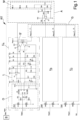
- reference RT globally indicates a three-phase synchronous rectifier, particularly usable in combination with a permanent magnet generator for the charge of the battery of a motor vehicle.
- the three-phase synchronous rectifier RT comprises three rectification units U A , U B , Uc provided with respective inputs connected to respective phases of a permanent magnet generator G and with respective outputs connected to a battery B of a vehicle.
- the rectification units U A , U B , Uc are configured to receive at input respective phase currents I A , I B , Ic of the generator G and to supply at output rectified currents I BATT A, I BATT B, I BATT C to be supplied to the battery B of the vehicle.
- Each of the rectification units U A , U B , Uc comprises a current sensor S', S" connected to a respective phase of the generator G and a respective output circuit O connected to the battery B and operatively connected to the current sensor S', S".
- the current sensor S', S" is configured to receive at input a respective phase current I A , I B , Ic, while the output circuit O is configured to be piloted by means of the current sensor S', S" to generate the rectified currents I BATT A, I BATT B, I BATT C.
- the current sensor S', S" comprises at least one toroidal element T made of a magnetic material crossed by a lead C which conveys the phase current I A , I B , Ic and at least one Hall effect sensor H1, H2, H connected to the toroidal element T and to the output circuit O.
- the three-phase synchronous rectifier RT can be implemented according to two possible and preferred embodiments: a first embodiment wherein the current sensor S' of each of the three rectification units U A , U B , U C comprises two digital unipolar Hall sensors H1 and H2 ( Figures 1-6 ); a second embodiment wherein the current sensor S" of each of the three rectification units U A , U B , Uc comprises one linear Hall sensor H ( Figures 7-10 ).
- the first possible embodiment of the three-phase synchronous rectifier RT according to the invention is described below, wherein the current sensor S' comprises two unipolar Hall effect magnetic sensors: a first unipolar Hall sensor H1 and a second unipolar Hall sensor H2. This first embodiment is illustrated in Figures 1-6 .
- the first and second unipolar Hall sensors H1, H2 are configured to be operate in the presence of respective and predefined levels of magnetic flux on the toroidal element (T).
- the three-phase synchronous rectifier RT is connected to a three-phase permanent magnet generator G.
- Figure 1 relates to a three-phase permanent magnet generator G wherein the three phase currents I A , I B , Ic like the three currents supplied to the battery I BATT A, I BATT B, I BATT C, have the same value but with phase displacement between one another by 120 degrees.
- the three currents I BATT A, I BATT B, I BATT C supplied to the battery add up to a single total current I BATT S supplied to the battery.
- the toroidal element T is provided with an air gap TR and the two unipolar Hall sensors H1, H2 are arranged inside the air gap TR side by side and rotated by 180 degrees the one with respect to the other.
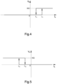
- the first unipolar Hall sensor H1 is configured to switch the output voltage V B from a low voltage value (0V) to a high voltage value (Vcc) at a first predefined threshold value I T1 , when the phase current I A (or I B and Ic with reference to the other phases) is positive and increasing.
- the first unipolar Hall sensor H1 is configured to switch the output voltage V B from the high voltage value (Vcc) to the low voltage value (0V) at a second predefined threshold value I' T1 .
- the first unipolar Hall sensor H1 is configured to create a hysteresis at the predefined switch threshold values I T1 , I' TI .
- Figure 5 shows the pattern of the output signal V A of the second unipolar Hall sensor H2 which, being flanked and rotated by 180° with respect to the first unipolar Hall sensor H1, possesses a similar behavior even if referred to the negative values of the phase current I A .
- the threshold values of the currents for the switch of the second Hall sensor H2 are I T2 and I' T2 respectively.
- the second unipolar Hall sensor H2 is configured to switch the output voltage V A from a low voltage value (0V) to a high voltage value (Vcc) at a first predefined threshold value I T2 , when the phase current I A (or I B and Ic with reference to the other phases) is negative and.
- the second unipolar Hall sensor H2 is configured to switch the output voltage V A from the high voltage value (Vcc) to the low voltage value (0V) at a second predefined threshold value I' T2 .
- the senor S' can comprise a plurality of windings of the lead C around at least one portion of the toroidal element T.
- the current values of the thresholds I T1 , I' T1 , I T2 , I' T2 it is possible to pass twice or more times, instead of only one as shown in Figure 2 , the lead that carries the phase current I A inside the magnetic toroidal element T.
- the current values of the thresholds I T1 , I' T1 , I T2 , I' T2 will be divided by the number of spirals of the lead C wound on the magnetic toroidal element T.
- the unipolar Hall sensors H1 and H2 are of the "open collector” type. Alternative embodiments cannot however be ruled out wherein, for example, the sensors are of the "push-pull” type.
- the output circuit O comprises at least a first Power MOS transistor Q1 and at least a second Power MOS transistor Q2 operatively connected to the current sensor S' (to the sensor S" with reference to the second embodiment) and adapted to be piloted by means of the current sensor S' (S") to generate the rectified currents I BATT A, I BATT B, I BATT C.
- the output circuit O comprises at least one half-bridge driver U2 operatively interposed between the current sensor S' (S") and the first and second Power MOS transistors Q1 and Q2.
- the half-bridge driver U2 is provided with a first input HI connected to the first unipolar Hall sensor H1 and with a second input LI connected to the second unipolar Hall sensor H2.
- the unipolar digital Hall sensors H1, H2 are usefully selected with response times short enough according to the electrical frequency of the generator G, so as not to generate excessive delays regarding the synchronization of the switch of the Power MOS transistors Q1 and Q2.
- the output signal V B of the first unipolar Hall sensor H1 switches to a high logic value.
- the output signal V B of the first unipolar Hall sensor H1 switches to a high logic value through the resistor R4.
- the logic value remains high until the current I A drops below the threshold value I' T1 .
- the half-bridge driver U2 is configured to pilot the output HO to the high value and, therefore, to positively polarize the gate of the Power MOS transistor Q1 through the resistor R10, thus sending the first transistor Q1 itself in conduction.
- the Power MOS transistor Q1 will remain in this state as long as the input HI of the half-bridge driver U2 remains at a high logic value.
- Zener diodes D3 and D5 The purpose of the Zener diodes D3 and D5 is to protect the Gates of the first and of the second Power MOS transistors Q1 and Q2, respectively.
- the output signal V A of the second unipolar Hall sensor H2 switches to a high logic value through the resistor R5, and remains high until the current I A climbs above the threshold value I' T2 .
- the signal V A is applied, through the resistor R11, to the input LI of the half-bridge driver U2 which pilots the output LO at high value and, therefore, positively polarizes the Gate of the second Power MOS transistor Q2 through the resistor R16, thus sending the second transistor Q2 itself in conduction.
- the second Power MOS transistor Q2 will remain in this state as long as the input LI of the half-bridge driver U2 remains at a high logic value.
- the half-bridge driver U2 powered by the voltage Vcci with the decoupling capacitor C1 at the typical value of 10 V, which may differ from the Vcc value, uses the capacitor C2 as "bootstrap charging" to pilot the gate of Q1 and also avoids the simultaneous conduction of the transistors Q1 and Q2.
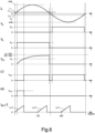
- FIG. 6 graphically illustrates the operation described above.
- phase current I A is lower in absolute value than the switching thresholds of the unipolar Hall sensors H1 and H2
- the circulation of the current occurs by means of the internal diodes of the Power Mos transistors Q1 and Q2.
- These diodes have a typical voltage drop of around 0.7V, which is why it is important to limit the aforementioned switch thresholds I T1 and I T2 to current values of around 3A, so as to limit dissipation during this transition phase before the Power Mos transistors Q1 and Q2 enter conduction.
- What has been described thus far is the operation relating to the synchronous rectification which represents the case in which all the current supplied by the permanent magnet generator G is supplied to the battery and loads of the vehicle.
- Such function is implemented by limiting the angle of conduction of the Power MOS transistor Q1 and at the same time putting in conduction the Power MOS transistor Q2 in the way described below.
- the three-phase synchronous rectifier RT advantageously comprises a current limiting circuit A, L configured to limit the current supplied by the generator G to the battery B in the event of the voltage V Batt supplied to the battery B exceeding a predefined desired value.
- the current limiting circuit A, L comprises an error amplifier circuit A configured to measure the voltage supplied to the battery V Batt and to supply a verification voltage signal Ve at output which varies between predefined voltage values acceptable for the correct operation of the battery.
- the error amplifier circuit A specifically comprises a measurement circuit M of the voltage V Batt supplied to the battery B.
- the measurement circuit M for measuring the voltage supplied to the battery V Batt comprises a couple of Zener diodes D1, D4 connected in series the one to the other and to a resistive divider R15, R28, R30.
- the battery voltage V Batt is measured by means of the Zener diodes D1 and D4 and by means of the resistive divider made up of the resistors R15, R28, R30.
- the resistive divider R15, R28, R30 together with a capacitor C4 furthermore constitutes a low-pass filter to limit the ripple on the battery voltage V Batt .
- the sum of the voltages of the two Zener diodes D1, D4 is selected between 13.0V and 13.6V in order to limit the current absorption from the battery with the endothermic motor of the generator Goff.
- the error amplifier circuit A comprises at least one operational amplifier U6 provided with a non-inverting input connected to a reference voltage and with an inverting input connected to the measurement circuit M.
- the operational amplifier U6 is configured to supply the verification voltage signal V e at output.
- the reference voltage is determined by the voltage drop onto a diode D6 when this is crossed by the current limited by a resistor R27 connected between the voltage Vcc and the anode of the diode D6 itself.
- the ratio between the resistance values of the resistors R26 and R29 connected between the inverting input and the output and between the inverting input and the measurement circuit M respectively which is approximately 100, determines the gain of the operational amplifier U6 in the inverting configuration.
- the verification voltage signal Ve present at the output of the operational amplifier U6 will vary linearly from a minimum acceptable voltage value to a maximum acceptable voltage value.
- the minimum acceptable voltage value may be 0V with a battery voltage of 14.4V
- the maximum acceptable voltage value may be V cc with a battery voltage of 14.6V. This excursion of the battery voltage value, which corresponds to the condition of full load and load absent at its ends respectively, is widely acceptable for the applications considered.
- the current limiting circuit A, L comprises, for each rectification unit U A , U B , Uc, at least one verification and limitation circuit L operatively connected to the current sensor S', to the error amplifier circuit A and to the output circuit O.
- the verification and limitation circuit L is configured to pilot the output circuit O, in order to make a phase control of the rectified current I BATT A (I BATT B, I BATT C) supplied to the battery B when the verification voltage signal Ve varies.
- the transistor Q5 When the output V B of the first unipolar Hall sensor H1 switches to a high logic value, the transistor Q5 will be piloted in conduction by means of the two resistors R18 and R23. At the same time, the transistor Q3 will be interdicted, because its base is not polarized, the current coming from the resistor R3 being short-circuit proof against earth by the transistor Q5.
- the capacitor C3 can charge itself with negative exponent rule at the asymptotic value resulting from the formula VCC ⁇ R20/(R2+R20).
- the signal V C3 is applied to the non-inverting input of the comparator U1, while to the inverting input is applied the output signal Ve of the operational amplifier U6.
- the output of the comparator U1 switches to the high logic value by means of the resistor R1.
- Such high logic value is applied by means of the diode D2 to the input LI of the half-bridge driver U2 and, by means of the resistive divider made up of the resistors R17 and R22, to the base of the transistor Q4, bringing it in conduction.
- the conduction of Q4 forces the input HI of the half-bridge driver U2 at a low logic value.
- the inputs LI and HI of the half-bridge driver U2 being at high and low logic value respectively, the outputs LO and HO of the driver itself will be at high and low logic value respectively, and so the second Power Mos transistor Q2 will be in conduction while the first Power Mos transistor Q1 will be interdicted.
- the current sensor S" comprises a magnetic linear Hall sensor H connected to the toroidal element T made of a magnetic material.
- the linear Hall sensor H is configured to generate an output voltage Vu which reproduces the pattern of the phase current I A (I B , Ic) in the lead C with a voltage offset equal to a predefined value.
- the toroidal element T is provided with an air gap TR and the linear Hall sensor H is arranged inside the air gap TR.
- the output voltage Vu of the sensor H reproduces the pattern of the current I A in the phase lead C with a voltage offset equal to Vcc/2.
- Such pattern of the voltage output Vu of the Hall sensor H is shown in Figure 10 .
- the current I A that passes inside the toroidal element T in ferrite induces a magnetic flow in the air gap TR proportionate to it which, in crossing the linear Hall sensor H, in turn generates an output voltage Vu with a value equal to V CC /2+(K ⁇ I A ), where K represents the proportionality constant between the current I A and the output voltage Vu.
- the current sensor S" comprises a first voltage comparator U1A and a second voltage comparator U1B.
- the linear Hall sensor H is connected to the inverting input of the first voltage comparator U1A and to the non-inverting input of the second voltage comparator U1B.
- the second voltage comparator U1B is configured to:
- the first voltage comparator U1A is configured to:
- the first voltage comparator U1A connected as shown in Figure 7 is configured to operate as an inverting voltage comparator with hysteresis and the trip threshold voltage values are defined by means of the resistance values selected for the resistors R7, R24 and R12.
- the second voltage comparator U1B connected as shown in Figure 7 is configured to operate as a non-inverting voltage comparator with hysteresis and the trip threshold voltage values are defined by means of the resistance values selected for the resistors R8, R25, R19 and R14.
- the trip voltage thresholds of the above comparators can be set by making reference to the current threshold values I T1 , I' T1 , I T2 and I' T2 already mentioned in case of use of the current sensor S' with two unipolar Hall sensors H1 and H2 described above, making use of the formula shown above for the calculation of the output voltage value Vu.
- the voltage threshold V T1 is set equal to the value V CC /2+(K ⁇ I T1 ).
- the output signals V A and V B of the two voltage comparators U1A and U1B will behave exactly like the output signals V A and V B of the two unipolar Hall sensors H1 and H2 considered previously with reference to the first possible embodiment, leaving unchanged the operation of the downstream circuit of the voltage comparators U1A and U1B themselves.
- Figure 10 shows the patterns of the signals described above in case of operation with a current sensor S" provided with a linear Hall sensor H.
- the battery current I BATT S is given by the sum of the 3 currents I BATT A, I BATT B and I BATT C relating to the 3 phases, identical to one another as regards value but out of phase by 120°. Having an effective balancing of the currents in the phases, we have as a consequence a "load sharing" among the phases themselves.
- This feature helps to optimize the efficiency of the generator-regulator system, thus avoiding overheating of one phase compared to the others, as in the case of currents in different phases.
- a current sensor consisting of a toroidal element made in a magnetic material, typically consisting of ferrite, crossed by the phase lead connected to the permanent magnet generator, together with the use of an air gap in the ferrite toroid inside which are placed one or two Hall sensors, makes it possible to accurately detect the zero-crossing of the current of the generator phases, while at the same time maintaining adequate response times of the synchronization system.
- the use of the Power MOS devices which possess the conduction resistance R DS(on) below 1m ⁇ , besides permitting low dissipation, allows a low voltage drop between the generator and the battery. In the case of a battery current of 40A, this drop passes from about 2V in the case of a three-phase diode or SCR bridge to just a few tenths of mV depending on the conduction resistance RDS(on) of the Power Mos transistor used.
- This characteristic therefore enables the generator to supply more current above all at low rotation speeds.
Landscapes
- Engineering & Computer Science (AREA)
- Power Engineering (AREA)
- Physics & Mathematics (AREA)
- General Physics & Mathematics (AREA)
- Control Of Eletrric Generators (AREA)
- Rectifiers (AREA)
- Charge And Discharge Circuits For Batteries Or The Like (AREA)
Claims (8)
- Dreiphasiger Synchrongleichrichter (RT) für ein Batterieladegerät an Bord eines Fahrzeugs, umfassend:drei Gleichrichtereinheiten (UA, UB, Uc), die mit jeweiligen Eingängen versehen sind, die mit jeweiligen Phasen eines Permanentmagnetgenerators (G) verbunden sind, und mit jeweiligen Ausgängen, die mit einer Batterie (B) eines Fahrzeugs verbunden sind,wobei die Gleichrichtereinheiten (UA, UB, Uc) dazu ausgebildet sind, am Eingang entsprechende Phasenströme (IA, IB, Ic) des Generators (G) zu empfangen und am Ausgang gleichgerichtete Ströme (IBATTA, IBATTB, IBATTC) zu liefern,und wobei jede der Gleichrichtereinheiten (UA, UB, Uc) einen Stromsensor (S', S"), der mit einer entsprechenden Phase des Generators (G) verbunden ist, und eine entsprechende Ausgangsschaltung (O) umfasst, die mit der Batterie verbunden ist und in Wirkverbindung mit dem Stromsensor (S', S") steht;wobei der Stromsensor (S', S") dazu ausgebildet ist, am Eingang einen jeweiligen Phasenstrom (IA, IB, Ic) zu empfangen, und die Ausgangsschaltung (O) dazu ausgebildet ist, mittels des Stromsensors (S', S") gesteuert zu werden, um die gleichgerichteten Ströme (IBATTA, IBATTB, IBATTC) zu erzeugen,wobei der Stromsensor (S', S") mindestens ein ringförmiges Element (T) aus einem magnetischen Material, das von einer Leitung (C) durchquert wird, die den Phasenstrom (IA, IB, Ic) überträgt, und mindestens einen Hallsensor (H1, H2, H) umfasst, der mit dem ringförmigen Element (T) und mit der Ausgangsschaltung (O) verbunden ist,dadurch gekennzeichnet, dass der Stromsensor (S') einen ersten digitalen unipolaren Hallsensor (H1) und einen zweiten digitalen unipolaren Hallsensor (H2) umfasst, die mit dem ringförmigen Element (T) aus einem magnetischen Material verbunden sind, wobei der erste und der zweite unipolare Hallsensor (H1, H2) dazu ausgebildet sind, bei Vorhandensein entsprechender und vordefinierter Niveaus des magnetischen Flusses an dem ringförmigen Element (T) zu arbeiten, wobei das ringförmige Element (T) mit einem Luftspalt (TR) versehen ist und der erste und der zweite Hallsensor (H1, H2) innerhalb des Luftspalts (TR) nebeneinander und um 180 Grad zueinander gedreht angeordnet sind, wobei der erste unipolare Hallsensor (H1) dazu ausgebildet ist, seine Ausgangsspannung (VB) von einem niedrigen Spannungswert (0V) zu einem hohen Spannungswert (Vcc) bei einem ersten vordefinierten positiven Schwellenwert (IT1) zu schalten, wenn der Phasenstrom (IA, IB, Ic) positiv ist und ansteigt, und um seine Ausgangsspannung (VB) von dem hohen Spannungswert (Vcc) auf den niedrigen Spannungswert (0V) bei einem zweiten vordefinierten positiven Schwellenwert (I'T1) zu schalten, wenn der Phasenstrom (IA, IB, Ic) positiv und abnehmend ist, und wobei der zweite unipolare Hallsensor (H2) dazu ausgebildet ist, seine Ausgangsspannung (VA) von dem niedrigen Spannungswert (0V) zu dem hohen Spannungswert (Vcc) bei einem ersten vordefinierten negativen Schwellenwert (IT2) zu schalten, wenn der Phasenstrom (IA, IB, Ic) negativ und abnehmend ist, und seine Ausgangsspannung (VA) von dem hohen Spannungswert (Vcc) auf den niedrigen Spannungswert (0V) bei einem zweiten vordefinierten negativen Schwellenwert (I'T2) zu schalten, wenn der Phasenstrom (IA, IB, Ic) 1 negativ und ansteigend ist,
oderdass der Stromsensor (S") einen magnetischen linearen Hallsensor (H) umfasst, der mit dem ringförmigen Element (T) aus einem magnetischen Material verbunden ist, wobei der lineare Hallsensor (H) dazu ausgebildet ist, eine Ausgangsspannung (Vu) zu erzeugen, die das Muster des Phasenstroms (IA, IB, Ic) in der Leitung (C) mit einem Spannungsversatz gleich einem vordefinierten Wert reproduziert, wobei das ringförmige Element (T) mit einem Luftspalt (TR) versehen ist und der lineare Hallsensor (H) innerhalb des Luftspalts (TR) angeordnet ist, wobei der Stromsensor (S") einen ersten Spannungskomparator (U1A) und einen zweiten Spannungskomparator (U1B) umfasst, wobei der lineare Hallsensor (H) mit dem invertierenden Eingang des ersten Spannungskomparators (U1A) und mit dem nicht-invertierenden Eingang des zweiten Spannungskomparators (U1 B) verbunden ist, wobei der zweite Spannungskomparator (U1B) dazu ausgebildet ist, seine Ausgangsspannung (VB) von einem niedrigen Spannungswert (0V) auf einen hohen Spannungswert (Vcc) bei einem ersten vordefinierten positiven Schwellenwert (IT1) zu schalten, wenn der Phasenstrom (IA, IB, Ic) positiv und ansteigend ist, und um seine Ausgangsspannung (VB) von dem hohen Spannungswert (Vcc) zu dem niedrigen Spannungswert (0V) bei einem zweiten vordefinierten positiven Schwellenwert (I'T1) zu schalten, wenn der Phasenstrom (IA, IB, Ic) positiv und abnehmend ist, und wobei der erste Spannungskomparator (U1A) dazu ausgebildet ist, seine Ausgangsspannung (VA) von dem niedrigen Spannungswert (0V) zu dem hohen Spannungswert (Vcc) bei einem ersten vordefinierten negativen Schwellenwert (VT2) zu schalten, wenn der Phasenstrom (IA, IB, Ic) negativ und abnehmend ist, und um seine Ausgangsspannung (VA) von dem hohen Spannungswert (Vcc) auf den niedrigen Spannungswert (0V) bei einem zweiten vordefinierten negativen Schwellenwert (V'T2) zu schalten, wenn der Phasenstrom (IA, IB, Ic) negativ und ansteigend ist. - Dreiphasiger Synchrongleichrichter (RT) nach Anspruch 1, dadurch gekennzeichnet, dass der Sensor (S', S") eine Mehrzahl von Wicklungen der Leitung (C) um mindestens einen Teil des ringförmigen Elements (T) umfasst.
- Dreiphasiger Synchrongleichrichter (RT) nach einem oder mehreren der vorhergehenden Ansprüche, dadurch gekennzeichnet, dass die Ausgangsschaltung (O) mindestens einen ersten Leistungs-MOS-Transistor (Q1) und mindestens einen zweiten Leistungs-MOS-Transistor (Q2) umfasst, die in Wirkverbindung mit dem Stromsensor (S', S") stehen und dazu ausgebildet sind, mittels des Stromsensors (S', S") angesteuert zu werden, um die gleichgerichteten Ströme (IBATTA, IBATTB, IBATTC) zu erzeugen.
- Dreiphasiger Synchrongleichrichter (RT) nach Anspruch 3, dadurch gekennzeichnet, dass die Ausgangsschaltung (O) mindestens einen Halbbrückentreiber (U2) umfasst, der zwischen dem Stromsensor (S', S") und dem ersten und zweiten Leistungs-MOS-Transistor (Q1, Q2) wirkend angeordnet ist.
- Dreiphasiger Synchrongleichrichter (RT) nach Anspruch 4, dadurch gekennzeichnet, dass der Halbbrückentreiber (U2) mit einem ersten Eingang (HI) versehen ist, der mit dem ersten unipolaren Hallsensor (H1) verbunden ist, und mit einem zweiten Eingang (LI), der mit dem zweiten unipolaren Hallsensor (H2) verbunden ist.
- Dreiphasiger Synchrongleichrichter (RT) nach einem oder mehreren der vorhergehenden Ansprüche, dadurch gekennzeichnet, dass er eine Strombegrenzungsschaltung (A, L) umfasst, die dazu ausgebildet ist, den von dem Generator (G) an die Batterie (B) gelieferten Strom zu begrenzen, wenn die an die Batterie (B) gelieferte Spannung (VBatt) einen vordefinierten Sollwert überschreitet.
- Dreiphasiger Synchrongleichrichter (RT) nach Anspruch 6, dadurch gekennzeichnet, dass die Strombegrenzungsschaltung (A, L) eine Fehlerverstärkerschaltung (A) umfasst, die dazu ausgebildet ist, die an die Batterie gelieferte Spannung (VBatt) zu messen und am Ausgang ein Prüfspannungssignal (Ve) zu liefern, das zwischen vordefinierten, für den korrekten Betrieb der Batterie akzeptablen Spannungswerten variiert.
- Dreiphasiger Synchrongleichrichter (RT) nach Anspruch 7, dadurch gekennzeichnet, dass die Fehlerverstärkerschaltung (A) eine Messschaltung (M) der an die Batterie (B) gelieferten Spannung (VBatt) umfasst.
Applications Claiming Priority (2)
| Application Number | Priority Date | Filing Date | Title |
|---|---|---|---|
| IT102018000003415A IT201800003415A1 (it) | 2018-03-09 | 2018-03-09 | Rettificatore sincrono trifase per caricabatteria a bordo veicolo |
| PCT/IB2019/051853 WO2019171320A1 (en) | 2018-03-09 | 2019-03-07 | Three-phase synchronous rectifier for battery charger on board vehicle |
Publications (2)
| Publication Number | Publication Date |
|---|---|
| EP3763014A1 EP3763014A1 (de) | 2021-01-13 |
| EP3763014B1 true EP3763014B1 (de) | 2024-08-07 |
Family
ID=62386832
Family Applications (1)
| Application Number | Title | Priority Date | Filing Date |
|---|---|---|---|
| EP19715222.6A Active EP3763014B1 (de) | 2018-03-09 | 2019-03-07 | Dreiphasiger synchrongleichrichter für batterieladegerät an bord eines fahrzeugs |
Country Status (6)
| Country | Link |
|---|---|
| US (1) | US11557913B2 (de) |
| EP (1) | EP3763014B1 (de) |
| CA (1) | CA3093510A1 (de) |
| ES (1) | ES2999339T3 (de) |
| IT (1) | IT201800003415A1 (de) |
| WO (1) | WO2019171320A1 (de) |
Families Citing this family (2)
| Publication number | Priority date | Publication date | Assignee | Title |
|---|---|---|---|---|
| IT202000008086A1 (it) | 2020-04-16 | 2021-10-16 | Ducati Energia S P A | Rettificatore sincrono trifase per la ricarica di una batteria a bordo veicolo |
| DE102020119340A1 (de) * | 2020-07-22 | 2022-01-27 | Phoenix Contact Gmbh & Co. Kg | Strommessgerät zur Messwerterfassung, Stromsensor sowie Strommessumformer |
Family Cites Families (7)
| Publication number | Priority date | Publication date | Assignee | Title |
|---|---|---|---|---|
| GB1461207A (en) * | 1975-04-01 | 1977-01-13 | Standard Telephones Cables Ltd | Electrical circuit for indicating the presence and direction of flow of an electrical current |
| JP2005304143A (ja) * | 2004-04-08 | 2005-10-27 | Mitsubishi Electric Corp | 電力変換装置 |
| ITMI20041026A1 (it) | 2004-05-24 | 2004-08-24 | Ducati Energia Spa | Regolatore di tensione a power mos per la ricarica di batterie |
| JP4990883B2 (ja) * | 2006-03-30 | 2012-08-01 | 新電元工業株式会社 | バッテリ充電装置、およびバッテリ充電装置における遅角制御方法 |
| JP5220589B2 (ja) | 2006-03-30 | 2013-06-26 | 新電元工業株式会社 | バッテリ充電装置、3相電圧生成回路、3相電圧生成方法、および遅角制御方法 |
| US9315109B2 (en) * | 2013-11-02 | 2016-04-19 | At&T Intellectual Property I, L.P. | Methods, systems, and products for charging batteries |
| US9762139B2 (en) * | 2014-08-12 | 2017-09-12 | Yiqiang Jake Zhang | Active switching rectifier employing MOSFET and current-based control using a hall-effect switch |
-
2018
- 2018-03-09 IT IT102018000003415A patent/IT201800003415A1/it unknown
-
2019
- 2019-03-07 CA CA3093510A patent/CA3093510A1/en active Pending
- 2019-03-07 ES ES19715222T patent/ES2999339T3/es active Active
- 2019-03-07 US US16/979,294 patent/US11557913B2/en active Active
- 2019-03-07 WO PCT/IB2019/051853 patent/WO2019171320A1/en not_active Ceased
- 2019-03-07 EP EP19715222.6A patent/EP3763014B1/de active Active
Also Published As
| Publication number | Publication date |
|---|---|
| ES2999339T3 (en) | 2025-02-25 |
| WO2019171320A1 (en) | 2019-09-12 |
| EP3763014A1 (de) | 2021-01-13 |
| IT201800003415A1 (it) | 2019-09-09 |
| US20210057931A1 (en) | 2021-02-25 |
| US11557913B2 (en) | 2023-01-17 |
| CA3093510A1 (en) | 2019-09-12 |
Similar Documents
| Publication | Publication Date | Title |
|---|---|---|
| US8541988B2 (en) | Rotary electric machine improved to carry out load-dump protection | |
| US6803748B2 (en) | System and method for controlling load dump voltage of a synchronous machine | |
| US7038406B2 (en) | Bi-directional field control for proportional control based generator/alternator voltage regulator | |
| US20110234176A1 (en) | Discharge control apparatus | |
| US20100320946A1 (en) | Brushless dc motor driver | |
| JP2816387B2 (ja) | 電源装置 | |
| TWI404327B (zh) | 永磁發電機之具可組態相位繞組連接之電壓調整器 | |
| US7298115B2 (en) | Control apparatus for a vehicular alternator | |
| US20030042809A1 (en) | Automotive alternator having detector for detecting initiation of rotation | |
| EP3763014B1 (de) | Dreiphasiger synchrongleichrichter für batterieladegerät an bord eines fahrzeugs | |
| JP3374543B2 (ja) | 車両用交流発電機の制御装置 | |
| US6696773B2 (en) | Vehicle generator control system | |
| US6670792B1 (en) | Alternator regulation circuit having parallel field coil current re-circulation | |
| US20080084191A1 (en) | Method and system for protecting voltage regulator driver circuitry during field coil short circuit condition | |
| US10516332B2 (en) | Induced voltage suppression device, motor system, and power conversion system | |
| EP0765021A1 (de) | Spannungsreglerschaltung für einen Dauermagnet-Wechselstromgenerator | |
| JPH11316249A (ja) | 電流検出回路および過電流保護回路 | |
| EP2068421B1 (de) | Spannungsregler und Generatoranordnung zum Laden von Batterien | |
| US12237797B2 (en) | Interface circuits for coupling hall sensors and resolvers to controllers in AC motor systems | |
| US6906480B2 (en) | Regulator control circuit and method | |
| JP5621375B2 (ja) | 車両用発電機 | |
| JP5144630B2 (ja) | 充電回路並びに充電回路を用いた発電機及び電動機 | |
| JP2000175486A (ja) | モータのリード線断線検出装置 | |
| CN117178466A (zh) | 包括保护装置的电压转换器 | |
| JP2015070621A (ja) | 整流装置及び半導体スイッチング素子の温度検出方法 |
Legal Events
| Date | Code | Title | Description |
|---|---|---|---|
| STAA | Information on the status of an ep patent application or granted ep patent |
Free format text: STATUS: UNKNOWN |
|
| STAA | Information on the status of an ep patent application or granted ep patent |
Free format text: STATUS: THE INTERNATIONAL PUBLICATION HAS BEEN MADE |
|
| PUAI | Public reference made under article 153(3) epc to a published international application that has entered the european phase |
Free format text: ORIGINAL CODE: 0009012 |
|
| STAA | Information on the status of an ep patent application or granted ep patent |
Free format text: STATUS: REQUEST FOR EXAMINATION WAS MADE |
|
| 17P | Request for examination filed |
Effective date: 20201007 |
|
| AK | Designated contracting states |
Kind code of ref document: A1 Designated state(s): AL AT BE BG CH CY CZ DE DK EE ES FI FR GB GR HR HU IE IS IT LI LT LU LV MC MK MT NL NO PL PT RO RS SE SI SK SM TR |
|
| AX | Request for extension of the european patent |
Extension state: BA ME |
|
| DAV | Request for validation of the european patent (deleted) | ||
| DAX | Request for extension of the european patent (deleted) | ||
| STAA | Information on the status of an ep patent application or granted ep patent |
Free format text: STATUS: EXAMINATION IS IN PROGRESS |
|
| 17Q | First examination report despatched |
Effective date: 20211026 |
|
| P01 | Opt-out of the competence of the unified patent court (upc) registered |
Effective date: 20230527 |
|
| GRAP | Despatch of communication of intention to grant a patent |
Free format text: ORIGINAL CODE: EPIDOSNIGR1 |
|
| STAA | Information on the status of an ep patent application or granted ep patent |
Free format text: STATUS: GRANT OF PATENT IS INTENDED |
|
| INTG | Intention to grant announced |
Effective date: 20240306 |
|
| GRAS | Grant fee paid |
Free format text: ORIGINAL CODE: EPIDOSNIGR3 |
|
| GRAA | (expected) grant |
Free format text: ORIGINAL CODE: 0009210 |
|
| STAA | Information on the status of an ep patent application or granted ep patent |
Free format text: STATUS: THE PATENT HAS BEEN GRANTED |
|
| AK | Designated contracting states |
Kind code of ref document: B1 Designated state(s): AL AT BE BG CH CY CZ DE DK EE ES FI FR GB GR HR HU IE IS IT LI LT LU LV MC MK MT NL NO PL PT RO RS SE SI SK SM TR |
|
| REG | Reference to a national code |
Ref country code: GB Ref legal event code: FG4D |
|
| REG | Reference to a national code |
Ref country code: CH Ref legal event code: EP |
|
| REG | Reference to a national code |
Ref country code: IE Ref legal event code: FG4D |
|
| REG | Reference to a national code |
Ref country code: DE Ref legal event code: R096 Ref document number: 602019056522 Country of ref document: DE |
|
| REG | Reference to a national code |
Ref country code: LT Ref legal event code: MG9D |
|
| REG | Reference to a national code |
Ref country code: NL Ref legal event code: MP Effective date: 20240807 |
|
| PG25 | Lapsed in a contracting state [announced via postgrant information from national office to epo] |
Ref country code: NO Free format text: LAPSE BECAUSE OF FAILURE TO SUBMIT A TRANSLATION OF THE DESCRIPTION OR TO PAY THE FEE WITHIN THE PRESCRIBED TIME-LIMIT Effective date: 20241107 |
|
| REG | Reference to a national code |
Ref country code: AT Ref legal event code: MK05 Ref document number: 1712013 Country of ref document: AT Kind code of ref document: T Effective date: 20240807 |
|
| PG25 | Lapsed in a contracting state [announced via postgrant information from national office to epo] |
Ref country code: NL Free format text: LAPSE BECAUSE OF FAILURE TO SUBMIT A TRANSLATION OF THE DESCRIPTION OR TO PAY THE FEE WITHIN THE PRESCRIBED TIME-LIMIT Effective date: 20240807 Ref country code: FI Free format text: LAPSE BECAUSE OF FAILURE TO SUBMIT A TRANSLATION OF THE DESCRIPTION OR TO PAY THE FEE WITHIN THE PRESCRIBED TIME-LIMIT Effective date: 20240807 Ref country code: PL Free format text: LAPSE BECAUSE OF FAILURE TO SUBMIT A TRANSLATION OF THE DESCRIPTION OR TO PAY THE FEE WITHIN THE PRESCRIBED TIME-LIMIT Effective date: 20240807 Ref country code: PT Free format text: LAPSE BECAUSE OF FAILURE TO SUBMIT A TRANSLATION OF THE DESCRIPTION OR TO PAY THE FEE WITHIN THE PRESCRIBED TIME-LIMIT Effective date: 20241209 Ref country code: GR Free format text: LAPSE BECAUSE OF FAILURE TO SUBMIT A TRANSLATION OF THE DESCRIPTION OR TO PAY THE FEE WITHIN THE PRESCRIBED TIME-LIMIT Effective date: 20241108 |
|
| PG25 | Lapsed in a contracting state [announced via postgrant information from national office to epo] |
Ref country code: BG Free format text: LAPSE BECAUSE OF FAILURE TO SUBMIT A TRANSLATION OF THE DESCRIPTION OR TO PAY THE FEE WITHIN THE PRESCRIBED TIME-LIMIT Effective date: 20240807 |
|
| PG25 | Lapsed in a contracting state [announced via postgrant information from national office to epo] |
Ref country code: LV Free format text: LAPSE BECAUSE OF FAILURE TO SUBMIT A TRANSLATION OF THE DESCRIPTION OR TO PAY THE FEE WITHIN THE PRESCRIBED TIME-LIMIT Effective date: 20240807 |
|
| PG25 | Lapsed in a contracting state [announced via postgrant information from national office to epo] |
Ref country code: AT Free format text: LAPSE BECAUSE OF FAILURE TO SUBMIT A TRANSLATION OF THE DESCRIPTION OR TO PAY THE FEE WITHIN THE PRESCRIBED TIME-LIMIT Effective date: 20240807 Ref country code: IS Free format text: LAPSE BECAUSE OF FAILURE TO SUBMIT A TRANSLATION OF THE DESCRIPTION OR TO PAY THE FEE WITHIN THE PRESCRIBED TIME-LIMIT Effective date: 20241207 |
|
| PG25 | Lapsed in a contracting state [announced via postgrant information from national office to epo] |
Ref country code: HR Free format text: LAPSE BECAUSE OF FAILURE TO SUBMIT A TRANSLATION OF THE DESCRIPTION OR TO PAY THE FEE WITHIN THE PRESCRIBED TIME-LIMIT Effective date: 20240807 |
|
| PG25 | Lapsed in a contracting state [announced via postgrant information from national office to epo] |
Ref country code: RS Free format text: LAPSE BECAUSE OF FAILURE TO SUBMIT A TRANSLATION OF THE DESCRIPTION OR TO PAY THE FEE WITHIN THE PRESCRIBED TIME-LIMIT Effective date: 20241107 |
|
| PG25 | Lapsed in a contracting state [announced via postgrant information from national office to epo] |
Ref country code: RS Free format text: LAPSE BECAUSE OF FAILURE TO SUBMIT A TRANSLATION OF THE DESCRIPTION OR TO PAY THE FEE WITHIN THE PRESCRIBED TIME-LIMIT Effective date: 20241107 Ref country code: PT Free format text: LAPSE BECAUSE OF FAILURE TO SUBMIT A TRANSLATION OF THE DESCRIPTION OR TO PAY THE FEE WITHIN THE PRESCRIBED TIME-LIMIT Effective date: 20241209 Ref country code: PL Free format text: LAPSE BECAUSE OF FAILURE TO SUBMIT A TRANSLATION OF THE DESCRIPTION OR TO PAY THE FEE WITHIN THE PRESCRIBED TIME-LIMIT Effective date: 20240807 Ref country code: NO Free format text: LAPSE BECAUSE OF FAILURE TO SUBMIT A TRANSLATION OF THE DESCRIPTION OR TO PAY THE FEE WITHIN THE PRESCRIBED TIME-LIMIT Effective date: 20241107 Ref country code: NL Free format text: LAPSE BECAUSE OF FAILURE TO SUBMIT A TRANSLATION OF THE DESCRIPTION OR TO PAY THE FEE WITHIN THE PRESCRIBED TIME-LIMIT Effective date: 20240807 Ref country code: LV Free format text: LAPSE BECAUSE OF FAILURE TO SUBMIT A TRANSLATION OF THE DESCRIPTION OR TO PAY THE FEE WITHIN THE PRESCRIBED TIME-LIMIT Effective date: 20240807 Ref country code: IS Free format text: LAPSE BECAUSE OF FAILURE TO SUBMIT A TRANSLATION OF THE DESCRIPTION OR TO PAY THE FEE WITHIN THE PRESCRIBED TIME-LIMIT Effective date: 20241207 Ref country code: HR Free format text: LAPSE BECAUSE OF FAILURE TO SUBMIT A TRANSLATION OF THE DESCRIPTION OR TO PAY THE FEE WITHIN THE PRESCRIBED TIME-LIMIT Effective date: 20240807 Ref country code: GR Free format text: LAPSE BECAUSE OF FAILURE TO SUBMIT A TRANSLATION OF THE DESCRIPTION OR TO PAY THE FEE WITHIN THE PRESCRIBED TIME-LIMIT Effective date: 20241108 Ref country code: FI Free format text: LAPSE BECAUSE OF FAILURE TO SUBMIT A TRANSLATION OF THE DESCRIPTION OR TO PAY THE FEE WITHIN THE PRESCRIBED TIME-LIMIT Effective date: 20240807 Ref country code: BG Free format text: LAPSE BECAUSE OF FAILURE TO SUBMIT A TRANSLATION OF THE DESCRIPTION OR TO PAY THE FEE WITHIN THE PRESCRIBED TIME-LIMIT Effective date: 20240807 Ref country code: AT Free format text: LAPSE BECAUSE OF FAILURE TO SUBMIT A TRANSLATION OF THE DESCRIPTION OR TO PAY THE FEE WITHIN THE PRESCRIBED TIME-LIMIT Effective date: 20240807 |
|
| REG | Reference to a national code |
Ref country code: ES Ref legal event code: FG2A Ref document number: 2999339 Country of ref document: ES Kind code of ref document: T3 Effective date: 20250225 |
|
| PG25 | Lapsed in a contracting state [announced via postgrant information from national office to epo] |
Ref country code: SM Free format text: LAPSE BECAUSE OF FAILURE TO SUBMIT A TRANSLATION OF THE DESCRIPTION OR TO PAY THE FEE WITHIN THE PRESCRIBED TIME-LIMIT Effective date: 20240807 Ref country code: RO Free format text: LAPSE BECAUSE OF FAILURE TO SUBMIT A TRANSLATION OF THE DESCRIPTION OR TO PAY THE FEE WITHIN THE PRESCRIBED TIME-LIMIT Effective date: 20240807 Ref country code: DK Free format text: LAPSE BECAUSE OF FAILURE TO SUBMIT A TRANSLATION OF THE DESCRIPTION OR TO PAY THE FEE WITHIN THE PRESCRIBED TIME-LIMIT Effective date: 20240807 |
|
| PG25 | Lapsed in a contracting state [announced via postgrant information from national office to epo] |
Ref country code: EE Free format text: LAPSE BECAUSE OF FAILURE TO SUBMIT A TRANSLATION OF THE DESCRIPTION OR TO PAY THE FEE WITHIN THE PRESCRIBED TIME-LIMIT Effective date: 20240807 |
|
| PG25 | Lapsed in a contracting state [announced via postgrant information from national office to epo] |
Ref country code: CZ Free format text: LAPSE BECAUSE OF FAILURE TO SUBMIT A TRANSLATION OF THE DESCRIPTION OR TO PAY THE FEE WITHIN THE PRESCRIBED TIME-LIMIT Effective date: 20240807 |
|
| PG25 | Lapsed in a contracting state [announced via postgrant information from national office to epo] |
Ref country code: SK Free format text: LAPSE BECAUSE OF FAILURE TO SUBMIT A TRANSLATION OF THE DESCRIPTION OR TO PAY THE FEE WITHIN THE PRESCRIBED TIME-LIMIT Effective date: 20240807 |
|
| REG | Reference to a national code |
Ref country code: DE Ref legal event code: R097 Ref document number: 602019056522 Country of ref document: DE |
|
| PLBE | No opposition filed within time limit |
Free format text: ORIGINAL CODE: 0009261 |
|
| STAA | Information on the status of an ep patent application or granted ep patent |
Free format text: STATUS: NO OPPOSITION FILED WITHIN TIME LIMIT |
|
| PGFP | Annual fee paid to national office [announced via postgrant information from national office to epo] |
Ref country code: ES Payment date: 20250401 Year of fee payment: 7 |
|
| 26N | No opposition filed |
Effective date: 20250508 |
|
| PG25 | Lapsed in a contracting state [announced via postgrant information from national office to epo] |
Ref country code: SE Free format text: LAPSE BECAUSE OF FAILURE TO SUBMIT A TRANSLATION OF THE DESCRIPTION OR TO PAY THE FEE WITHIN THE PRESCRIBED TIME-LIMIT Effective date: 20240807 |
|
| PG25 | Lapsed in a contracting state [announced via postgrant information from national office to epo] |
Ref country code: MC Free format text: LAPSE BECAUSE OF FAILURE TO SUBMIT A TRANSLATION OF THE DESCRIPTION OR TO PAY THE FEE WITHIN THE PRESCRIBED TIME-LIMIT Effective date: 20240807 |
|
| REG | Reference to a national code |
Ref country code: CH Ref legal event code: H13 Free format text: ST27 STATUS EVENT CODE: U-0-0-H10-H13 (AS PROVIDED BY THE NATIONAL OFFICE) Effective date: 20251023 |
|
| PG25 | Lapsed in a contracting state [announced via postgrant information from national office to epo] |
Ref country code: LU Free format text: LAPSE BECAUSE OF NON-PAYMENT OF DUE FEES Effective date: 20250307 |
|
| GBPC | Gb: european patent ceased through non-payment of renewal fee |
Effective date: 20250307 |
|
| REG | Reference to a national code |
Ref country code: BE Ref legal event code: MM Effective date: 20250331 |
|
| PG25 | Lapsed in a contracting state [announced via postgrant information from national office to epo] |
Ref country code: GB Free format text: LAPSE BECAUSE OF NON-PAYMENT OF DUE FEES Effective date: 20250307 |
|
| PG25 | Lapsed in a contracting state [announced via postgrant information from national office to epo] |
Ref country code: IT Free format text: LAPSE BECAUSE OF NON-PAYMENT OF DUE FEES Effective date: 20250307 |
|
| PG25 | Lapsed in a contracting state [announced via postgrant information from national office to epo] |
Ref country code: BE Free format text: LAPSE BECAUSE OF NON-PAYMENT OF DUE FEES Effective date: 20250331 |
|
| PG25 | Lapsed in a contracting state [announced via postgrant information from national office to epo] |
Ref country code: CH Free format text: LAPSE BECAUSE OF NON-PAYMENT OF DUE FEES Effective date: 20250331 |
|
| PG25 | Lapsed in a contracting state [announced via postgrant information from national office to epo] |
Ref country code: IE Free format text: LAPSE BECAUSE OF NON-PAYMENT OF DUE FEES Effective date: 20250307 |
|
| PGFP | Annual fee paid to national office [announced via postgrant information from national office to epo] |
Ref country code: DE Payment date: 20260327 Year of fee payment: 8 |
|
| PG25 | Lapsed in a contracting state [announced via postgrant information from national office to epo] |
Ref country code: IT Free format text: LAPSE BECAUSE OF NON-PAYMENT OF DUE FEES Effective date: 20250307 |
|
| PGFP | Annual fee paid to national office [announced via postgrant information from national office to epo] |
Ref country code: IT Payment date: 20260323 Year of fee payment: 8 |
|
| PGRI | Patent reinstated in contracting state [announced from national office to epo] |
Ref country code: IT Effective date: 20250731 |
|
| PGFP | Annual fee paid to national office [announced via postgrant information from national office to epo] |
Ref country code: FR Payment date: 20260325 Year of fee payment: 8 |