EP3763720B1 - Composé et dispositif électroluminescent organique le comprenant - Google Patents
Composé et dispositif électroluminescent organique le comprenant Download PDFInfo
- Publication number
- EP3763720B1 EP3763720B1 EP19793229.6A EP19793229A EP3763720B1 EP 3763720 B1 EP3763720 B1 EP 3763720B1 EP 19793229 A EP19793229 A EP 19793229A EP 3763720 B1 EP3763720 B1 EP 3763720B1
- Authority
- EP
- European Patent Office
- Prior art keywords
- compound
- layer
- preparation
- chemical formula
- group
- Prior art date
- Legal status (The legal status is an assumption and is not a legal conclusion. Google has not performed a legal analysis and makes no representation as to the accuracy of the status listed.)
- Active
Links
Images
Classifications
-
- C—CHEMISTRY; METALLURGY
- C07—ORGANIC CHEMISTRY
- C07F—ACYCLIC, CARBOCYCLIC OR HETEROCYCLIC COMPOUNDS CONTAINING ELEMENTS OTHER THAN CARBON, HYDROGEN, HALOGEN, OXYGEN, NITROGEN, SULFUR, SELENIUM OR TELLURIUM
- C07F7/00—Compounds containing elements of Groups 4 or 14 of the Periodic Table
- C07F7/02—Silicon compounds
- C07F7/08—Compounds having one or more C—Si linkages
- C07F7/0803—Compounds with Si-C or Si-Si linkages
- C07F7/081—Compounds with Si-C or Si-Si linkages comprising at least one atom selected from the elements N, O, halogen, S, Se or Te
- C07F7/0812—Compounds with Si-C or Si-Si linkages comprising at least one atom selected from the elements N, O, halogen, S, Se or Te comprising a heterocyclic ring
- C07F7/0816—Compounds with Si-C or Si-Si linkages comprising at least one atom selected from the elements N, O, halogen, S, Se or Te comprising a heterocyclic ring said ring comprising Si as a ring atom
-
- C—CHEMISTRY; METALLURGY
- C07—ORGANIC CHEMISTRY
- C07D—HETEROCYCLIC COMPOUNDS
- C07D405/00—Heterocyclic compounds containing both one or more hetero rings having oxygen atoms as the only ring hetero atoms, and one or more rings having nitrogen as the only ring hetero atom
- C07D405/14—Heterocyclic compounds containing both one or more hetero rings having oxygen atoms as the only ring hetero atoms, and one or more rings having nitrogen as the only ring hetero atom containing three or more hetero rings
-
- C—CHEMISTRY; METALLURGY
- C07—ORGANIC CHEMISTRY
- C07D—HETEROCYCLIC COMPOUNDS
- C07D409/00—Heterocyclic compounds containing two or more hetero rings, at least one ring having sulfur atoms as the only ring hetero atoms
- C07D409/14—Heterocyclic compounds containing two or more hetero rings, at least one ring having sulfur atoms as the only ring hetero atoms containing three or more hetero rings
-
- C—CHEMISTRY; METALLURGY
- C07—ORGANIC CHEMISTRY
- C07D—HETEROCYCLIC COMPOUNDS
- C07D417/00—Heterocyclic compounds containing two or more hetero rings, at least one ring having nitrogen and sulfur atoms as the only ring hetero atoms, not provided for by group C07D415/00
- C07D417/14—Heterocyclic compounds containing two or more hetero rings, at least one ring having nitrogen and sulfur atoms as the only ring hetero atoms, not provided for by group C07D415/00 containing three or more hetero rings
-
- C—CHEMISTRY; METALLURGY
- C09—DYES; PAINTS; POLISHES; NATURAL RESINS; ADHESIVES; COMPOSITIONS NOT OTHERWISE PROVIDED FOR; APPLICATIONS OF MATERIALS NOT OTHERWISE PROVIDED FOR
- C09K—MATERIALS FOR MISCELLANEOUS APPLICATIONS, NOT PROVIDED FOR ELSEWHERE
- C09K11/00—Luminescent materials, e.g. electroluminescent or chemiluminescent
- C09K11/06—Luminescent materials, e.g. electroluminescent or chemiluminescent containing organic luminescent materials
-
- H—ELECTRICITY
- H10—SEMICONDUCTOR DEVICES; ELECTRIC SOLID-STATE DEVICES NOT OTHERWISE PROVIDED FOR
- H10K—ORGANIC ELECTRIC SOLID-STATE DEVICES
- H10K50/00—Organic light-emitting devices
- H10K50/10—OLEDs or polymer light-emitting diodes [PLED]
- H10K50/14—Carrier transporting layers
- H10K50/15—Hole transporting layers
-
- H—ELECTRICITY
- H10—SEMICONDUCTOR DEVICES; ELECTRIC SOLID-STATE DEVICES NOT OTHERWISE PROVIDED FOR
- H10K—ORGANIC ELECTRIC SOLID-STATE DEVICES
- H10K50/00—Organic light-emitting devices
- H10K50/10—OLEDs or polymer light-emitting diodes [PLED]
- H10K50/14—Carrier transporting layers
- H10K50/16—Electron transporting layers
-
- H—ELECTRICITY
- H10—SEMICONDUCTOR DEVICES; ELECTRIC SOLID-STATE DEVICES NOT OTHERWISE PROVIDED FOR
- H10K—ORGANIC ELECTRIC SOLID-STATE DEVICES
- H10K50/00—Organic light-emitting devices
- H10K50/10—OLEDs or polymer light-emitting diodes [PLED]
- H10K50/17—Carrier injection layers
- H10K50/171—Electron injection layers
-
- H—ELECTRICITY
- H10—SEMICONDUCTOR DEVICES; ELECTRIC SOLID-STATE DEVICES NOT OTHERWISE PROVIDED FOR
- H10K—ORGANIC ELECTRIC SOLID-STATE DEVICES
- H10K85/00—Organic materials used in the body or electrodes of devices covered by this subclass
- H10K85/40—Organosilicon compounds, e.g. TIPS pentacene
-
- H—ELECTRICITY
- H10—SEMICONDUCTOR DEVICES; ELECTRIC SOLID-STATE DEVICES NOT OTHERWISE PROVIDED FOR
- H10K—ORGANIC ELECTRIC SOLID-STATE DEVICES
- H10K85/00—Organic materials used in the body or electrodes of devices covered by this subclass
- H10K85/60—Organic compounds having low molecular weight
- H10K85/649—Aromatic compounds comprising a hetero atom
- H10K85/654—Aromatic compounds comprising a hetero atom comprising only nitrogen as heteroatom
-
- H—ELECTRICITY
- H10—SEMICONDUCTOR DEVICES; ELECTRIC SOLID-STATE DEVICES NOT OTHERWISE PROVIDED FOR
- H10K—ORGANIC ELECTRIC SOLID-STATE DEVICES
- H10K85/00—Organic materials used in the body or electrodes of devices covered by this subclass
- H10K85/60—Organic compounds having low molecular weight
- H10K85/649—Aromatic compounds comprising a hetero atom
- H10K85/657—Polycyclic condensed heteroaromatic hydrocarbons
-
- H—ELECTRICITY
- H10—SEMICONDUCTOR DEVICES; ELECTRIC SOLID-STATE DEVICES NOT OTHERWISE PROVIDED FOR
- H10K—ORGANIC ELECTRIC SOLID-STATE DEVICES
- H10K85/00—Organic materials used in the body or electrodes of devices covered by this subclass
- H10K85/60—Organic compounds having low molecular weight
- H10K85/649—Aromatic compounds comprising a hetero atom
- H10K85/657—Polycyclic condensed heteroaromatic hydrocarbons
- H10K85/6574—Polycyclic condensed heteroaromatic hydrocarbons comprising only oxygen in the heteroaromatic polycondensed ring system, e.g. cumarine dyes
-
- H—ELECTRICITY
- H10—SEMICONDUCTOR DEVICES; ELECTRIC SOLID-STATE DEVICES NOT OTHERWISE PROVIDED FOR
- H10K—ORGANIC ELECTRIC SOLID-STATE DEVICES
- H10K85/00—Organic materials used in the body or electrodes of devices covered by this subclass
- H10K85/60—Organic compounds having low molecular weight
- H10K85/649—Aromatic compounds comprising a hetero atom
- H10K85/657—Polycyclic condensed heteroaromatic hydrocarbons
- H10K85/6576—Polycyclic condensed heteroaromatic hydrocarbons comprising only sulfur in the heteroaromatic polycondensed ring system, e.g. benzothiophene
-
- C—CHEMISTRY; METALLURGY
- C09—DYES; PAINTS; POLISHES; NATURAL RESINS; ADHESIVES; COMPOSITIONS NOT OTHERWISE PROVIDED FOR; APPLICATIONS OF MATERIALS NOT OTHERWISE PROVIDED FOR
- C09K—MATERIALS FOR MISCELLANEOUS APPLICATIONS, NOT PROVIDED FOR ELSEWHERE
- C09K2211/00—Chemical nature of organic luminescent or tenebrescent compounds
- C09K2211/10—Non-macromolecular compounds
- C09K2211/1018—Heterocyclic compounds
-
- H—ELECTRICITY
- H10—SEMICONDUCTOR DEVICES; ELECTRIC SOLID-STATE DEVICES NOT OTHERWISE PROVIDED FOR
- H10K—ORGANIC ELECTRIC SOLID-STATE DEVICES
- H10K2101/00—Properties of the organic materials covered by group H10K85/00
- H10K2101/10—Triplet emission
-
- H—ELECTRICITY
- H10—SEMICONDUCTOR DEVICES; ELECTRIC SOLID-STATE DEVICES NOT OTHERWISE PROVIDED FOR
- H10K—ORGANIC ELECTRIC SOLID-STATE DEVICES
- H10K50/00—Organic light-emitting devices
- H10K50/10—OLEDs or polymer light-emitting diodes [PLED]
- H10K50/11—OLEDs or polymer light-emitting diodes [PLED] characterised by the electroluminescent [EL] layers
-
- H—ELECTRICITY
- H10—SEMICONDUCTOR DEVICES; ELECTRIC SOLID-STATE DEVICES NOT OTHERWISE PROVIDED FOR
- H10K—ORGANIC ELECTRIC SOLID-STATE DEVICES
- H10K50/00—Organic light-emitting devices
- H10K50/10—OLEDs or polymer light-emitting diodes [PLED]
- H10K50/11—OLEDs or polymer light-emitting diodes [PLED] characterised by the electroluminescent [EL] layers
- H10K50/12—OLEDs or polymer light-emitting diodes [PLED] characterised by the electroluminescent [EL] layers comprising dopants
-
- H—ELECTRICITY
- H10—SEMICONDUCTOR DEVICES; ELECTRIC SOLID-STATE DEVICES NOT OTHERWISE PROVIDED FOR
- H10K—ORGANIC ELECTRIC SOLID-STATE DEVICES
- H10K50/00—Organic light-emitting devices
- H10K50/10—OLEDs or polymer light-emitting diodes [PLED]
- H10K50/17—Carrier injection layers
-
- H—ELECTRICITY
- H10—SEMICONDUCTOR DEVICES; ELECTRIC SOLID-STATE DEVICES NOT OTHERWISE PROVIDED FOR
- H10K—ORGANIC ELECTRIC SOLID-STATE DEVICES
- H10K50/00—Organic light-emitting devices
- H10K50/10—OLEDs or polymer light-emitting diodes [PLED]
- H10K50/18—Carrier blocking layers
Definitions
- the present disclosure relates to a compound represented by Chemical Formula 1, and an organic light emitting device including the same.
- An organic light emission phenomenon generally refers to a phenomenon converting electrical energy to light energy using an organic material.
- An organic light emitting device using an organic light emission phenomenon normally has a structure including an anode, a cathode, and an organic material layer therebetween.
- the organic material layer is formed in a multilayer structure formed with different materials in order to increase efficiency and stability of the organic light emitting device, and for example, may be formed with a hole injection layer, a hole transfer layer, a light emitting layer, an electron transfer layer, an electron injection layer and the like.
- the present specification is directed to providing a compound represented by Chemical Formula 1.
- the present specification is directed to providing an organic light emitting device having, by including the compound represented by Chemical Formula 1, a low driving voltage, high efficiency, or excellent lifetime properties.
- Chemical Formula 1 One embodiment of the present specification provides a compound represented by the following Chemical Formula 1.
- Chemical Formula 1 In Chemical Formula 1,
- an organic light emitting device comprising a first electrode, a second electrode, and one or more organic material layers provided between the first electrode and the second electrode, wherein the organic material layer comprises the compound represented by Chemical Formula 1 described above.
- a compound represented by Chemical Formula 1 can be included in a hole injection layer; a hole transfer layer; a layer carrying out hole transfer and injection at the same time; a hole control layer; an electron control layer; an electron injection layer; an electron transfer layer and a layer carrying out electron transfer and injection at the same time; and particularly in a light emitting layer of an organic light emitting device.
- an organic light emitting device including the compound of Chemical Formula 1 can have enhanced efficiency, lowered driving voltage, or enhanced lifetime properties.
- One embodiment of the present disclosure provides a compound represented by Chemical Formula 1.
- a term such as ⁇ include' or 'have' means the presence of features or constituents described in the specification, and is not to exclude in advance the possibility of adding one or more other features or constituents.
- a description of a part such as a region or a layer being provided above or on another part includes not only a case of the part being directly above the another part but a case of still another region, layer or the like being provided therebetween.
- an aryl group means a totally or partially unsaturated substituted or unsubstituted monocyclic ring or polycyclic ring.
- the aryl group has 6 to 25 carbon atoms.
- the aryl group has 6 to 20 carbon atoms.
- the aryl group has 6 to 18 carbon atoms.
- the aryl group has 6 to 13 carbon atoms.
- the aryl group has 6 to 12 carbon atoms.
- the aryl group has 6 carbon atoms.
- the aryl group may be a monocyclic aryl group or a polycyclic aryl group.
- Examples of the monocyclic aryl group may include a phenyl group, a biphenyl group, a terphenyl group and the like, but are not limited thereto.
- Examples of the polycyclic aryl group may include a naphthyl group, an anthracenyl group, a phenanthrenyl group, a perylenyl group, a fluoranthenyl group, a triphenylenyl group, a pyrenyl group, a tetracenyl group, a chrysenyl group, a fluorenyl group, an indenyl group, an acenaphthyl group, a benzofluorenyl group and the like, but are not limited thereto.
- the fluorenyl group may be substituted, and two substituents may bond to each other to form a spiro structure.
- Examples of the substituted fluorenyl group may include and the like, but are not limited thereto.
- the heteroaryl group is a cyclic group including one or more of N, O and S as a heteroatom, and although not limited thereto, the number of carbon atoms is preferably from 2 to 40. According to one embodiment, the number of carbon atoms of the heteroaryl group is from 2 to 30. According to another embodiment, the number of carbon atoms of the heteroaryl group is from 2 to 20.
- heteroaryl group may include a thiophenyl group, a furanyl group, a pyrrolyl group, an imidazolyl group, a thiazolyl group, an oxazolyl group, an oxadiazolyl group, a triazolyl group, a pyridinyl group, a bipyridinyl group, a pyrimidinyl group, a diazinyl group, a triazinyl group, a triazolyl group, an acridinyl group, a carbolinyl group, an acenaphthoquinoxalinyl group, an indenoquinazolinyl group, an indenoisoquinolinyl group, an indenoquinolinyl group, a pyridoindolyl group, a pyridazinyl group, a pyrazinyl group, a quinolinyl group, a quinazol
- X1 is O
- X2 is O or SiRcRd.
- X1 is SiRaRb
- X2 is O or SiRcRd.
- X1 is O
- X2 is O
- X1 is SiRaRb
- X2 is O
- X1 is O
- X2 is SiRcRd.
- X1 is SiRaRb
- X2 is SiRcRd
- Ra to Rd are the same as or different from each other, and each independently hydrogen; deuterium; an alkyl group having 1 to 10 carbon atoms; or an aryl group having 6 to 20 carbon atoms.
- Ra to Rd are the same as or different from each other, and each independently hydrogen; deuterium; an alkyl group having 1 to 6 carbon atoms; or an aryl group having 6 to 13 carbon atoms.
- Ra to Rd are the same as or different from each other, and each independently hydrogen; deuterium; an alkyl group having 1 to 4 carbon atoms; or an aryl group having 6 to 10 carbon atoms.
- Ra to Rd are the same as or different from each other, and each independently hydrogen; deuterium; a methyl group; or a phenyl group.
- any one of A1 to A4 is a linking group bonding to triazine, any one is Ar1, the rest are hydrogen, and A'1 to A'4 are hydrogen.
- any one of A1 to A4 is a linking group bonding to triazine, the rest are hydrogen, any one of A'1 to A'4 is Ar1, and the rest are hydrogen.
- any one of B1 to B4 is a linking group bonding to triazine, any one is Ar2, the rest are hydrogen, and B'1 to B'4 are hydrogen.
- any one of B1 to B4 is a linking group bonding to triazine, the rest are hydrogen, any one of B'1 to B'4 is Ar2, and the rest are hydrogen.
- an aromatic 6-membered ring included in the compound represented by Chemical Formula 1 is 10 or less.
- Chemical Formula 1 includes 11 or more aromatic 6-membered rings, a sublimation temperature of the compound increases due to an increase in the molecular weight, which may cause a problem in device thermal stability.
- triazine includes one aromatic 6-membered ring
- benzofuran includes two aromatic 6-membered rings (benzene rings).
- Ar1 and Ar2 are the same as or different from each other, and each independently an aryl group; or a heteroaryl group unsubstituted or substituted with an aryl group and comprising one or more of N, O and S.
- Ar1 and Ar2 are the same as or different from each other, and each independently an aryl group; or a heteroaryl group unsubstituted or substituted with an aryl group and comprising a pentagonal ring.
- Ar1 and Ar2 are the same as or different from each other, and each independently an aryl group having 6 to 25 carbon atoms; or a heteroaryl group having 2 to 25 carbon atoms unsubstituted or substituted with an aryl group.
- Ar1 and Ar2 are the same as or different from each other, and each independently an aryl group; or a heteroaryl group unsubstituted or substituted with an aryl group having 6 to 18 carbon atoms.
- Ar1 and Ar2 are the same as or different from each other, and each independently an aryl group; or a heteroaryl group unsubstituted or substituted with an aryl group having 6 to 12 carbon atoms.
- Ar1 and Ar2 are the same as or different from each other, and each independently an aryl group; or a heteroaryl group unsubstituted or substituted with an aryl group and comprising pyrrole, furan, thiophene, imidazole, oxazole or thiazole.
- Ar1 and Ar2 are the same as or different from each other, and each independently an aryl group having 6 to 20 carbon atoms; or a heteroaryl group having 2 to 20 carbon atoms unsubstituted or substituted with an aryl group.
- Ar1 and Ar2 are the same as or different from each other, and each independently an aryl group having 6 to 20 carbon atoms; or a heteroaryl group having 7 to 20 carbon atoms unsubstituted or substituted with an aryl group.
- Ar1 and Ar2 are the same as or different from each other, and each independently an aryl group having 6 to 18 carbon atoms; or a heteroaryl group having 2 to 24 carbon atoms unsubstituted or substituted with an aryl group.
- Ar1 and Ar2 are the same as or different from each other, and each independently an aryl group having 6 to 18 carbon atoms; or a heteroaryl group having 2 to 20 carbon atoms unsubstituted or substituted with an aryl group.
- Ar1 and Ar2 are the same as or different from each other, and each independently an aryl group having 6 to 18 carbon atoms; or a heteroaryl group having 2 to 16 carbon atoms unsubstituted or substituted with an aryl group.
- Ar1 and Ar2 are the same as or different from each other, and each independently an aryl group having 6 to 18 carbon atoms; or a heteroaryl group having 2 to 20 carbon atoms unsubstituted or substituted with an aryl group.
- Ar1 and Ar2 are the same as or different from each other, and each independently an aryl group having 6 to 15 carbon atoms; or a heteroaryl group having 2 to 20 carbon atoms unsubstituted or substituted with an aryl group.
- Ar1 and Ar2 are the same as or different from each other, and each independently an aryl group having 6 to 13 carbon atoms; or a heteroaryl group having 2 to 16 carbon atoms unsubstituted or substituted with an aryl group.
- Ar1 and Ar2 are the same as or different from each other, and each independently an aryl group having 6 to 12 carbon atoms; or a heteroaryl group having 2 to 12 carbon atoms unsubstituted or substituted with an aryl group.
- Ar1 and Ar2 are the same as or different from each other, and each independently a phenyl group; a biphenyl group; a terphenyl group; a dibenzothiophenyl group; a dibenzofuranyl group; a carbazolyl group unsubstituted or substituted with a phenyl group; a benzothiazolyl group; a benzimidazolyl group unsubstituted or substituted with a phenyl group; or a benzoxazolyl group.
- Chemical Formula 1 is represented by any one of the following Chemical Formula 2 to Chemical Formula 4.
- a linking unit bonding to triazine among A1 to A4 is Ax (x is an integer of 1 to 4)
- a linking unit bonding to triazine among B1 to B4 is By (y is an integer of 1 to 4)
- a linking unit bonding to Ar1 among A'1 to A'4 is A'x' (x' is an integer of 1 to 4)
- a linking unit bonding to Ar2 among B'1 to B'4 is B'y' (y' is an integer of 1 to 4)
- x is the same as y
- x' is the same as y' .
- a linking unit bonding to triazine among A1 to A4 is Am (m is an integer of 1 to 4)
- a linking unit bonding to triazine among B1 to B4 is Bn (n is an integer of 1 to 4)
- a linking unit bonding to Ar1 among A1 to A4 is Am' (m' is an integer of 1 to 4)
- a linking unit bonding to Ar2 among B'1 to B'4 is B'n' (n' is an integer of 1 to 4)
- m is the same as n
- m' is the same as n' .
- a linking unit bonding to triazine among A1 to A4 is Ap (p is an integer of 1 to 4)
- a linking unit bonding to triazine among B1 to B4 is Bq (q is an integer of 1 to 4)
- a linking unit bonding to Ar1 among A1 to A4 is Ap' (p' is an integer of 1 to 4)
- a linking unit bonding to Ar2 among B1 to B4 is Bq' (q' is an integer of 1 to 4)
- p is the same as q
- p' is the same as q'.
- Chemical Formula 1 is represented by any one of the following Chemical Formula 1-A to Chemical Formula 1-C.
- Ra to Rd, A1 to A4, A'1 to A'4, B1 to B4 and B'1 to B'4 have the same definitions as in Chemical Formula 1.
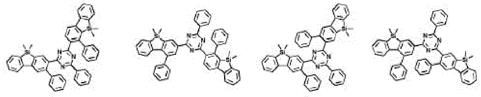
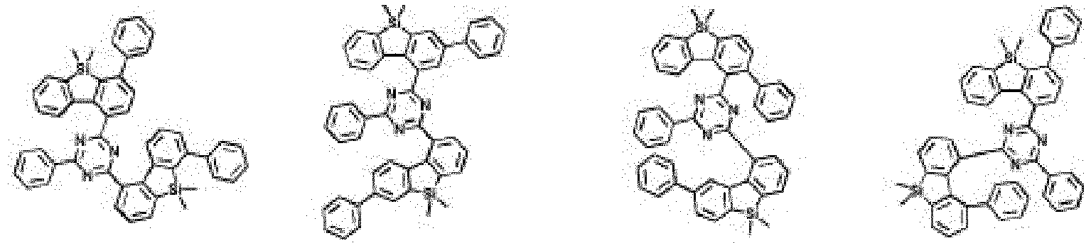
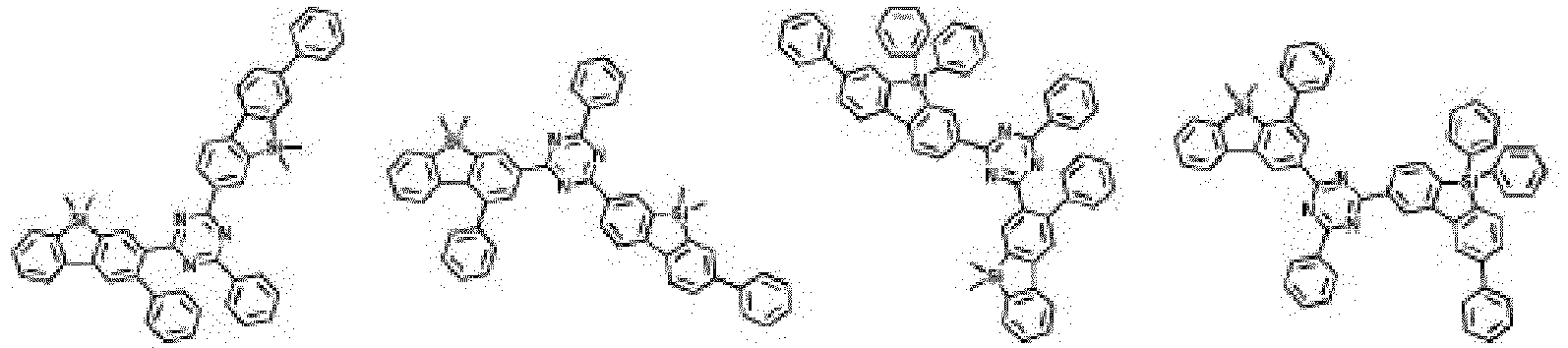
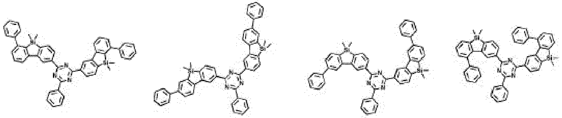
- the compound represented by Chemical Formula 1 is any one selected from among the following compounds.
- the compound represented by Chemical Formula 1 described above may be prepared according to the following General Formula 1 or General Formula 2.
- Ra to Rd, Ar1 and Ar2 have the same definitions as in Chemical Formula 1.
- General Formulae 1 and 2 are one example of methods for forming the compound represented by Chemical Formula 1, and a method for synthesizing the compound represented by Chemical Formula 1 is not limited to General Formulae 1 and 2, and methods known in the art may be used.
- One embodiment of the present specification provides an organic light emitting device comprising the compound represented by Chemical Formula 1.
- One embodiment of the present specification provides an organic light emitting device comprising a first electrode, a second electrode, and one or more organic material layers provided between the first electrode and the second electrode, wherein the organic material layer comprises the compound represented by Chemical Formula 1 described above.
- the organic material layer of the organic light emitting device of the present specification may be formed in a single layer structure, but may also be formed in a multilayer structure in which two or more organic material layers are laminated.
- the organic light emitting device of the present disclosure may have a structure comprising a hole injection layer, a hole transfer layer, a layer carrying out hole transfer and injection at the same time, a hole control layer, a light emitting layer, an electron control layer, an electron transfer layer, an electron injection layer, a layer carrying out electron transfer and injection at the same time and the like as the organic material layer.
- the organic material layer comprising the compound represented by Chemical Formula 1 has a thickness of 5 nm or greater; 10 nm or greater; 20 nm or greater; or 30 nm or greater, and 80 nm or less; 70 nm or less; 60 nm or less; or 50 nm or less.
- the organic material layer comprises a light emitting layer
- the light emitting layer comprises the compound represented by Chemical Formula 1.
- the light emitting layer comprising the compound represented by Chemical Formula 1 has a thickness of 25 nm to 55 nm; or 30 nm to 50 nm.
- the organic material layer comprising the compound represented by Chemical Formula 1 further includes a host.
- the light emitting layer comprising the compound represented by Chemical Formula 1 further comprises a host.
- the light emitting layer including the compound represented by Chemical Formula 1 further comprises a host, device lifetime properties may be greatly enhanced.
- the host is a carbazole derivative; or a biscarbazole derivative.
- the host is a substituted or unsubstituted biscarbazole.
- the host is a compound represented by the following Chemical Formula H.
- Chemical Formula H In Chemical Formula H,
- Ar11 and Ar12 are the same as or different from each other, and each independently a substituted or unsubstituted aryl group; or a substituted or unsubstituted heteroaryl group.
- Ar11 and Ar12 are the same as or different from each other, and each independently a substituted or unsubstituted aryl group having 6 to 30 carbon atoms; or a substituted or unsubstituted heteroaryl group having 2 to 30 carbon atoms.
- Ar11 and Ar12 are the same as or different from each other, and each independently a substituted or unsubstituted aryl group having 6 to 18 carbon atoms; or a substituted or unsubstituted heteroaryl group having 2 to 15 carbon atoms.
- Ar11 and Ar12 are the same as or different from each other, and each independently an aryl group unsubstituted or substituted with an aryl group or a heteroaryl group; or a heteroaryl group unsubstituted or substituted with an aryl group or a heteroaryl group.
- Ar11 and Ar12 are the same as or different from each other, and each independently a phenyl group; a biphenyl group; or a triazinyl group unsubstituted or substituted with a phenyl group or a biphenyl group.
- Ar13 and Ar14 are the same as or different from each other, and each independently hydrogen; deuterium; an alkyl group; an aryl group unsubstituted or substituted with an aryl group or a heteroaryl group; or a heteroaryl group unsubstituted or substituted with an aryl group or a heteroaryl group.
- Ar13 and Ar14 are the same as or different from each other, and each independently hydrogen; a methyl group; a phenyl group; a biphenyl group; or a carbazolyl group unsubstituted or substituted with a phenyl group.
- Ar13 and Ar14 are the same as or different from each other, and each independently hydrogen; or deuterium.
- L11 and L12 are the same as or different from each other, and each independently a direct bond; a substituted or unsubstituted divalent aryl group having 6 to 20 carbon atoms; or a substituted or unsubstituted divalent heteroaryl group having 2 to 20 carbon atoms.
- L11 and L12 are the same as or different from each other, and each independently a direct bond; a divalent aryl group unsubstituted or substituted with an aryl group; or a divalent heteroaryl group unsubstituted or substituted with an aryl group.
- L11 and L12 are the same as or different from each other, and each independently a direct bond; or a phenylene group.
- the light emitting layer comprising the compound represented by Chemical Formula 1 further comprises a dopant.
- the light emitting layer comprising the compound represented by Chemical Formula 1 further comprises a dopant, and a content of the dopant is greater than or equal to 0.1 parts by weight and less than or equal to 20 parts by weight; or greater than or equal to 1 parts by weight and less than or equal to 15 parts by weight with respect to a total 100 parts by weight of the light emitting layer.
- the dopant is an iridium complex.
- the dopant is a compound represented by the following Chemical Formula Dp.
- Chemical Formula Dp is a compound represented by the following Chemical Formula Dp.
- Cy is an aromatic hydrocarbon ring; or an aromatic heteroring.
- Cy is an aromatic hydrocarbon ring; or an aromatic heteroring comprising at least one element selected form the group consisting of N, S and O.
- Cy is an aromatic ring having 3 to 14 carbon atoms.
- Cy is an aromatic ring having 3 to 10 carbon atoms.
- Cy is benzene; thiophene; or benzothiophene.
- Chemical Formula Dp is represented by the following Chemical Formula Dp' .
- Chemical Formula Dp' is represented by the following Chemical Formula Dp' .
- the organic light emitting device may be an organic light emitting device having a normal structure in which an anode, one or more organic material layers and a cathode are consecutively laminated on a substrate (normal type).
- the organic light emitting device may be an organic light emitting device having a structure in a reverse direction in which a cathode, one or more organic material layers and an anode are consecutively laminated on a substrate (inverted type).
- the first electrode is an anode
- the second electrode is a cathode
- the first electrode is a cathode
- the second electrode is an anode
- the organic light emitting device may have structures as illustrated in FIGs. 1 and 2 .
- the organic light emitting device may be formed with a substrate (1), an anode (2), an organic material layer (3) and a cathode (4).
- the compound represented by Chemical Formula 1 is included in the organic material layer (3).
- the organic light emitting device may be formed with a substrate (1), an anode (2), a hole injection layer (5), a hole transfer layer (6), a hole control layer (7), a light emitting layer (8), an electron transfer layer (9), an electron injection layer (10) and a cathode (4).
- the compound represented by Chemical Formula 1 is included in the light emitting layer (8).
- the compound represented by Chemical Formula 1 is included in any one of the hole transfer layer (5), the hole transfer layer (6) and the hole control layer (7).
- the compound represented by Chemical Formula 1 is included in the electron transfer layer (9) or the electron injection layer (10).
- the structure of the organic light emitting device is not limited to FIG. 1 and FIG. 2 , and may be any one of the following structures.
- the organic material layers may be formed with materials the same as or different from each other.
- the organic light emitting device of the present specification may be manufactured by consecutively laminating a first electrode, an organic material layer and a second electrode on a substrate.
- the organic light emitting device may be manufactured by forming an anode on a substrate by depositing a metal, a metal oxide having conductivity, or an alloy thereof using a physical vapor deposition (PVD) method such as sputtering or e-beam evaporation, and forming an organic material layer including a hole injection layer, a hole transfer layer, a light emitting layer and an electron transfer layer thereon, and then depositing a material capable of being used as a cathode thereon.
- PVD physical vapor deposition
- the compound represented by Chemical Formula 1 may be formed into an organic material layer using a solution coating method as well as a vacuum deposition method when manufacturing the organic light emitting device.
- the solution coating method means spin coating, dip coating, doctor blading, inkjet printing, screen printing, a spray method, roll coating and the like, but is not limited thereto.
- the organic light emitting device may also be manufactured by consecutively depositing a cathode material, an organic material layer and an anode material on a substrate (International Patent Application Laid-Open Publication No. 2003/012890).
- the manufacturing method is not limited thereto.
- anode material materials having large work function are normally preferred so that hole injection to an organic material layer is smooth.
- the anode material capable of being used in the present disclosure include metals such as vanadium, chromium, copper, zinc and gold, or alloys thereof; metal oxides such as zinc oxide, indium oxide, indium tin oxide (ITO) and indium zinc oxide (IZO); combinations of metals and oxides such as ZnO:Al or SnO 2 :Sb; conductive polymers such as poly(3-methylthiophene), poly[3,4-(ethylene-1,2-dioxy)thiophene] (PEDOT), polypyrrole and polyaniline, but are not limited thereto.
- the cathode material materials having small work function are normally preferred so that electron injection to an organic material layer is smooth.
- the cathode material include metals such as magnesium, calcium, sodium, potassium, titanium, indium, yttrium, lithium, gadolinium, aluminum, silver, tin and lead, or alloys thereof; multilayer structure materials such as LiF/Al or LiO 2 /Al, and the like, but are not limited thereto.
- the hole injection layer is a layer injecting holes received from an electrode to a light emitting layer or an adjacent layer provided on a light emitting layer side.
- the hole injection material compounds having an ability to transfer holes, therefore, having a hole injection effect in an anode, having an excellent hole injection effect for a light emitting layer or a light emitting material, preventing excitons generated in the light emitting layer from moving to an electron injection layer or an electron injection material, and in addition thereto, having an excellent thin film forming ability are preferably used.
- the highest occupied molecular orbital (HOMO) of the hole injection material is preferably in between the work function of an anode material and the HOMO of surrounding organic material layers.
- the hole injection material examples include metal porphyrins, oligothiophene, arylamine-based organic materials, hexanitrile hexaazatriphenylene-based organic materials, quinacridone-based organic materials, perylene-based organic materials, anthraquinone, and polyaniline- and polythiophene-based conductive polymers, and the like, but are not limited thereto.
- the hole transfer layer is a layer receiving holes from a hole injection layer and transferring the holes to a light emitting layer or an adjacent layer provided on a light emitting layer side.
- the hole transfer material materials capable of receiving holes from an anode or a hole injection layer, moving the holes to a light emitting layer, and having high mobility for the holes are suited.
- the hole transfer material include arylamine-based organic materials, conductive polymers, block copolymers having conjugated parts and non-conjugated parts together, and the like, but are not limited thereto.
- the hole control layer is a layer controlling performance of a whole device by preventing electrons inflowing from a light emitting layer to an anode and by controlling a flow of holes inflowing to the light emitting layer.
- the hole control material compounds having abilities of preventing electrons inflowing from a light emitting layer to an anode, and controlling a flow of holes injected to the light emitting layer or the light emitting material are preferred.
- arylamine-based organic materials may be used as the hole control layer, however, the hole control layer is not limited thereto.
- the light emitting material is a material capable of emitting light in a visible light region by receiving holes and electrons from a hole transfer layer and an electron transfer layer, respectively, and binding the holes and the electrons, and is preferably a material having favorable quantum efficiency for fluorescence or phosphorescence.
- Alq 3 8-hydroxy-quinoline aluminum complexes
- carbazole-based compounds dimerized styryl compounds
- BAlq 10-hydroxybenzoquinoline-metal compounds
- benzoxazole-, benzothiazole- and benzimidazole-based compounds poly(p-phenylenevinylene) (PPV)-based polymers
- spiro compounds polyfluorene; rubrene, and the like, but are not limited thereto.
- the light emitting layer may include a host material and a dopant material.
- the host material may include fused aromatic ring derivatives, heteroring-containing compounds or the like. Specifically, as the fused aromatic ring derivative, anthracene derivatives, pyrene derivatives, naphthalene derivatives, pentacene derivatives, phenanthrene compounds, fluoranthene compounds and the like may be included, and as the heteroring-containing compound, carbazole derivatives, dibenzofuran derivatives, ladder-type furan compounds, pyrimidine derivatives and the like may be included, however, the host material is not limited thereto.
- the dopant material of the light emitting layer may include aromatic amine derivatives, styrylamine compounds, boron complexes, fluoranthene compounds, metal complexes and the like.
- the aromatic amine derivative is a fused aromatic ring derivative having a substituted or unsubstituted arylamine group, and arylamine group-including pyrene, anthracene, chrysene, peryflanthene and the like may be used.
- styrylamine compound compounds in which substituted or unsubstituted arylamine is substituted with at least one arylvinyl group may be used.
- styralamine compound may include styrylamine, styryldiamine, styryltriamine, styryltetramine and the like, but are not limited thereto.
- metal complex iridium complexes, platinum complexes and the like may be used, however, the metal complex is not limited thereto.
- the electron control layer is a layer controlling performance of a whole device by blocking holes inflowing from a light emitting layer to a cathode and by controlling electrons inflowing to the light emitting layer.
- the electron control material compounds having abilities of preventing holes inflowing from a light emitting layer to a cathode, and controlling electrons injected to the light emitting layer or the light emitting material are preferred.
- the electron control material proper materials may be used depending on the constitution of the organic material layers used in a device.
- the electron control layer is placed between a light emitting layer and a cathode, and is preferably provided directly in contact with a light emitting layer.
- the electron transfer layer is a layer receiving electrons from an electron injection layer and transferring the electrons to a light emitting layer.
- the electron transfer material materials capable of favorably receiving electrons from a cathode, moving the electrons to a light emitting layer, and having high mobility for the electrons are suited.
- the electron transfer material may include Al complexes of 8-hydroxyquinoline; complexes including Alq 3 ; organic radical compounds; hydroxyflavon-metal complexes, and the like, but are not limited thereto.
- the electron transfer layer may be used together with any desired cathode material as used in the art. In one embodiment, as the cathode material, materials having low work function; and an aluminum layer or a silver layer may be used.
- Examples of the material having low work function may include cesium, barium, calcium, ytterbium, samarium and the like, and after forming a layer with the above-mentioned material, an aluminum layer or a silver layer may be formed on the layer.
- the electron injection layer is a layer injecting electrons received from an electrode to a light emitting layer.
- the electron injection material compounds having an electron transferring ability, having an electron injection effect from a cathode, having an excellent electron injection effect for a light emitting layer or light emitting material, and preventing excitons generated in the light emitting layer from moving to a hole injection layer, and in addition thereto, having an excellent thin film forming ability are preferably used.
- fluorenone anthraquinodimethane, diphenoquinone, thiopyran dioxide, oxazole, oxadiazole, triazole, imidazole, perylene tetracarboxylic acid, fluorenylidene methane, anthrone or the like, and derivatives thereof, metal complex compounds, nitrogen-containing 5-membered ring derivatives, and the like, but are not limited thereto.
- the metal complex compound includes 8-hydroxyquinolinato lithium, bis(8-hydroxyquinolinato)zinc, bis(8-hydroxyquinolinato)copper, bis(8-hydroxyquinolinato)manganese, tris(8-hydroxyquinolinato)aluminum, tris(2-methyl-8-hydroxyquinolinato) aluminum, tris(8-hydroxyquinolinato)gallium, bis(10-hydroxybenzo[h]quinolinato)beryllium, bis(10-hydroxybenzo[h]quinolinato)zinc, bis(2-methyl-8-quinolinato)chlorogallium, bis(2-methyl-8-quinolinato)(o-cresolato)gallium, bis(2-methyl-8-quinolinato)(1-naphtholato)aluminum, bis(2-methyl-8-quinolinato)(2-naphtholato)gallium and the like, but is not limited thereto.
- the organic light emitting device may be a top-emission type, a bottom-emission type or a dual-emission type depending on the materials used.
- Fluoro-2-iodobenzene (66 g, 299.99 mmol) and (3-bromo-6-chloro-2-hydroxyphenyl)boronic acid (75.38 g, 299.99 mmol) were dissolved in tetrahydrofuran (THF) (800 ml).
- THF tetrahydrofuran
- a 2 M sodium carbonate (Na 2 CO 3 ) solution (500 mL) and tetrakis(triphenylphosphine)palladium (0) [Pd(PPh 3 ) 4 ] (10.4 g, 9 mmol) were introduced thereto, and the result was refluxed for 12 hours.
- 1,3-Dibromo-4-chloro-2-nitrobenzene (87.03 g, 275.98 mmol) and (2-nitrophenyl)boronic acid (46.1 g, 275.98 mmol) were dissolved in tetrahydrofuran (THF) (800 ml).
- THF tetrahydrofuran
- a 2 M sodium carbonate (Na 2 CO 3 ) solution (500 mL)
- tetrakis(triphenylphosphine)palladium(0) [Pd(PPh 3 ) 4 ] (9.6 g, 8.28 mmol) were introduced thereto, and the result was refluxed for 6 hours at 50°C.
- a glass substrate on which indium tin oxide (ITO) was coated as a thin film to a thickness of 130 nm was placed in detergent-dissolved distilled water and ultrasonic cleaned.
- ITO indium tin oxide
- a product of Fischer Co. was used as the detergent, and as the distilled water, distilled water filtered twice with a filter manufactured by Millipore Co. was used.
- the substrate was ultrasonic cleaned with solvents of isopropyl alcohol, acetone and methanol, then dried, and then transferred to a plasma cleaner.
- the substrate was cleaned for 5 minutes using oxygen plasma, and then transferred to a vacuum depositor.
- a hole injection layer was formed by thermal vacuum depositing the following Compound HI-1 to a thickness of 5 nm.
- a hole transfer layer was formed on the hole injection layer by thermal vacuum depositing the following Compound HT-1 to a thickness of 25 nm, and on the HT-1 deposited film, a hole control layer was formed by vacuum depositing the following Compound HT-2 to a thickness of 5 nm.
- a light emitting layer having a thickness of 40 nm was formed on the HT-2 deposited film by co-depositing Compound 1 prepared above and the following Compound Dp-25 in a weight ratio of 88:12.
- an electron transfer layer was formed by vacuum depositing the following Compound ET-1 to a thickness of 25 nm, and an electron injection layer was formed thereon by vacuum depositing (thickness 10 nm) the following Compound ET-2 and LiQ in a weight ratio of 98:2.
- a cathode was formed by depositing aluminum to a thickness of 100 nm.
- Examples 19 to 24 and Comparative Examples 5 and 6 organic light emitting devices were manufactured in the same manner as in Example 1 except that compounds described in the following Table 1 were used in a weight ratio of 1:1 instead of Compound 1. Taking Example 19 as an example, Compound 1 and Compound H-2 were used in a weight ratio of 1:1 instead of Compound 1 in Example 1.
- T 95 means time taken for luminance decreasing to 95% when employing initial luminance at current density of 20 mA/cm 2 as 100%.
- Examples 1 to 18 and Comparative Examples 1 and 2 are examples of a device using a single host in a light emitting layer.
- Compound C1 used in Comparative Example 1 is a compound in which triazine is substituted with two dibenzothiophenyl groups. From Table 1, it was identified that the devices of Examples 1 to 18 had lifetime properties enhanced by approximately 55% to 88% compared to the device of Comparative Example 1.
- Compound C2 used in Comparative Example 2 is a compound in which triazine is substituted with one dibenzofuranyl group and two aryl groups. From Table 1, it was identified that the devices of Examples 1 to 18 had lifetime properties enhanced by approximately 37% to 75% compared to the device of Comparative Example 2.
- Compound C3 used in Comparative Example 3 is a compound in which a phenyl group, one of substituents of the triazine, is substituted with a heteroaryl group. From Table 1, it was identified that the devices of Examples 1 to 18 had current efficiency enhanced by approximately 4.3% to 15.5% compared to the device of Comparative Example 3.
- Compound C4 used in Comparative Example 4 is a compound in which one dibenzofuranyl group of the two dibenzofuranyl groups, a substituent of the triazine, is unsubstituted. From Table 1, it was identified that the devices of Examples 1 to 18 had current efficiency enhanced by approximately 4.7% to 17% compared to the device of Comparative Example 4.
- Examples 19 to 24 are examples of a device using two types of hosts in a light emitting layer. When comparing Examples 19 to 24 and Examples 1 to 18, it was identified that, when using two types of hosts in a light emitting layer, current efficiency increased more, and particularly, lifetime properties were significantly enhanced.
- the devices of Examples 19 to 24 using the compound of the present disclosure also had excellent current efficiency and lifetime properties compared to the devices of Comparative Examples 5 and 6.
- a dibenzofuranyl group and/or a dibenzosilole group directly bond to triazine having strong electron properties, and the dibenzofuranyl group and/or the dibenzosilole group are substituted with an aryl group and a heteroaryl group having strong hole properties.
- the compound represented by Chemical Formula 1 of the present disclosure may be understood to have advantages in terms of device efficiency and lifetime since holes and electros are smoothly inflowing, and holes and electrons are well balanced.
Landscapes
- Chemical & Material Sciences (AREA)
- Organic Chemistry (AREA)
- Engineering & Computer Science (AREA)
- Materials Engineering (AREA)
- Physics & Mathematics (AREA)
- Spectroscopy & Molecular Physics (AREA)
- Optics & Photonics (AREA)
- Electroluminescent Light Sources (AREA)
- Plural Heterocyclic Compounds (AREA)
Claims (9)
- Composé représenté par la formule chimique suivante
 X1 est O ou SiRaRb ;X2 est O ou SiRcRd ;Ra à Rd sont identiques ou différents les uns des autres, et chacun indépendamment de l'hydrogène ; du deutérium ; un groupe alkyle ; ou un groupe aryle ;l'un quelconque de A1 à A4 et A'1 à A'4 est un groupe de liaison se liant à la triazine, l'un quelconque est Ar1, et le reste est de l'hydrogène ;l'un quelconque de B1 à B4 et B'1 à B'4 est un groupe de liaison se liant à la triazine, l'un quelconque est Ar2, et le reste est de l'hydrogène ; etdans lequel Ar1 et Ar2 sont identiques ou différents l'un de l'autre, et chacun indépendamment un groupe aryle ; ou un groupe hétéroaryle non substitué ou substitué par un groupe aryle.
 - Composé selon la revendication 1, dans lequel la formule chimique 1 est représentée par l'une quelconque des formules chimiques 2 à 4 suivantes :
dans les formules chimiques 2 à 4 suivantes, X1, X2, Ar1 et Ar2 présentent les mêmes définitions que dans la formule chimique (1),
 l'un quelconque de A1 à A4 est un groupe de liaison se liant à la triazine, et le reste est de l'hydrogène ;l'un quelconque de A'1 à A'4 est Ar1, et le reste est de l'hydrogène ;l'un quelconque de B1 à B4 est un groupe de liaison se liant à la triazine, et le reste est de l'hydrogène ; etl'un quelconque de B'1 à B'4 est Ar2, et le reste est de l'hydrogène,
 l'un quelconque de A1 à A4 est un groupe de liaison se liant à la triazine, l'un quelconque est Ar1, et le reste est de l'hydrogène ;l'un quelconque de B1 à B4 est un groupe de liaison se liant à la triazine, et le reste est de l'hydrogène ; et l'un quelconque de B'1 à B'4 est Ar2, et le reste est de l'hydrogène,
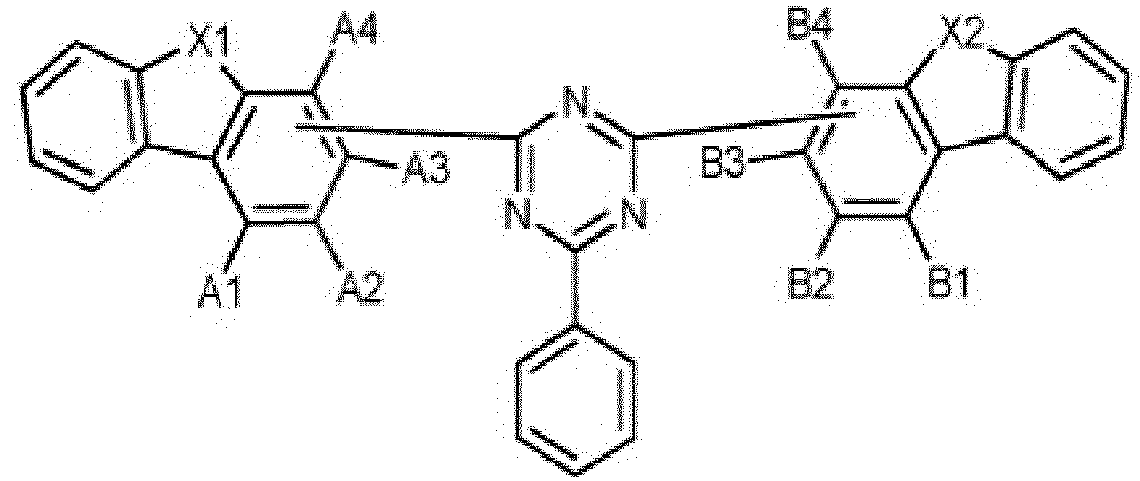 l'un quelconque de A1 à A4 est un groupe de liaison se liant à la triazine, l'un quelconque est Ar1, et le reste est de l'hydrogène ; etl'un quelconque de B1 à B4 est un groupe de liaison se liant à la triazine, l'un quelconque est Ar2, et le reste est de l'hydrogène.
 - Composé selon la revendication 1, dans lequel la formule chimique 1 est représentée par l'une quelconque des formules chimiques 1-A à 1-C suivantes :


Ra à Rd, A1 à A4, A'1 à A'4, B1 à B4 et B'1 à B'4 présentent les mêmes définitions que dans la formule chimique 1. - Composé selon la revendication 1, dans lequel Ar1 et Ar2 sont identiques ou différents l'un de l'autre, et chacun indépendamment un groupe aryle présentant 6 à 25 atomes de carbone ; ou un groupe hétéroaryle présentant 2 à 25 atomes de carbone non substitué ou substitué par un groupe aryle.
- Composé selon la revendication 1, dans lequel le composé représenté par la formule chimique 1 est l'un quelconque sélectionné parmi les composés suivants :





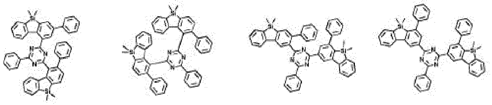
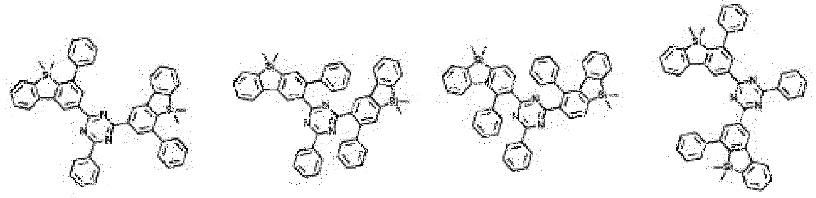









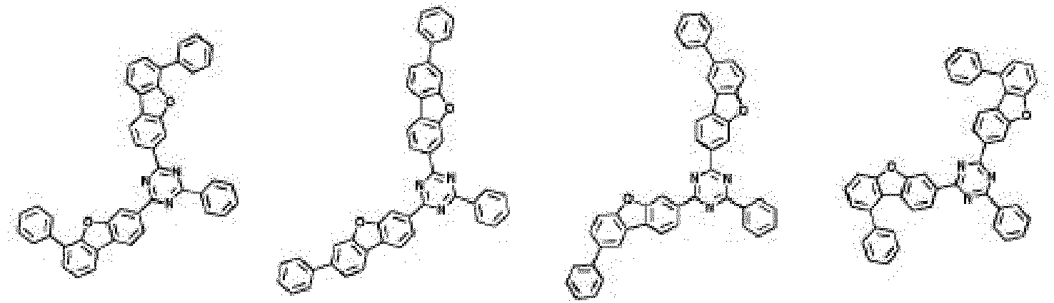


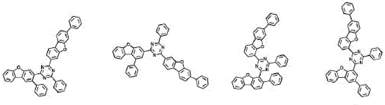


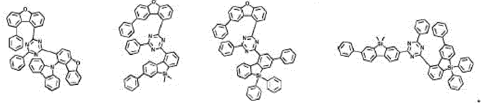
- Dispositif électroluminescent organique comprenant :une première électrode ;une seconde électrode ; etune ou plusieurs couches de matériau organique disposées entre la première électrode et la seconde électrode,dans lequel la couche de matériau organique comprend le composé représenté par la formule chimique 1 selon l'une quelconque des revendications 1 à 5.
- Dispositif électroluminescent organique selon la revendication 6, dans lequel la couche de matériau organique comprend une couche électroluminescente, et la couche électroluminescente comprend le composé représenté par la formule chimique 1.
- Dispositif électroluminescent organique selon la revendication 7, dans lequel la couche électroluminescente comprenant le composé représenté par la formule chimique 1 comprend en outre un dopant.
- Dispositif électroluminescent organique selon la revendication 6, dans lequel la couche de matériau organique comprend une couche d'injection de trous ; une couche de transfert de trous ; une couche réalisant le transfert et l'injection de trous en même temps ; une couche de commande de trous ; une couche de commande d'électrons ; une couche d'injection d'électrons ; une couche de transfert d'électrons ; ou une couche réalisant le transfert et l'injection d'électrons en même temps, et la couche d'injection de trous ; la couche de transfert de trous ; la couche réalisant le transfert et l'injection de trous en même temps ; la couche de commande de trous ; la couche de commande d'électrons ; la couche d'injection d'électrons ; la couche de transfert d'électrons ; ou la couche réalisant le transfert et l'injection d'électrons en même temps comprend le composé représenté par la formule chimique 1.
Applications Claiming Priority (2)
| Application Number | Priority Date | Filing Date | Title |
|---|---|---|---|
| KR20180047968 | 2018-04-25 | ||
| PCT/KR2019/004983 WO2019209037A1 (fr) | 2018-04-25 | 2019-04-25 | Composé et dispositif électroluminescent organique le comprenant |
Publications (3)
| Publication Number | Publication Date |
|---|---|
| EP3763720A1 EP3763720A1 (fr) | 2021-01-13 |
| EP3763720A4 EP3763720A4 (fr) | 2021-04-14 |
| EP3763720B1 true EP3763720B1 (fr) | 2023-11-22 |
Family
ID=68295564
Family Applications (1)
| Application Number | Title | Priority Date | Filing Date |
|---|---|---|---|
| EP19793229.6A Active EP3763720B1 (fr) | 2018-04-25 | 2019-04-25 | Composé et dispositif électroluminescent organique le comprenant |
Country Status (5)
| Country | Link |
|---|---|
| US (1) | US11980089B2 (fr) |
| EP (1) | EP3763720B1 (fr) |
| KR (1) | KR102202771B1 (fr) |
| CN (1) | CN111971289B (fr) |
| WO (1) | WO2019209037A1 (fr) |
Families Citing this family (5)
| Publication number | Priority date | Publication date | Assignee | Title |
|---|---|---|---|---|
| KR102720177B1 (ko) * | 2018-03-29 | 2024-10-21 | 덕산네오룩스 주식회사 | 유기전기소자용 화합물, 이를 이용한 유기전기소자 및 그 전자 장치 |
| KR102235480B1 (ko) * | 2018-10-22 | 2021-04-02 | 주식회사 엘지화학 | 신규한 헤테로 고리 화합물 및 이를 이용한 유기발광 소자 |
| CN111039938B (zh) * | 2019-12-20 | 2021-01-05 | 陕西莱特光电材料股份有限公司 | 有机电致发光材料、电子器件及电子装置 |
| WO2021221475A1 (fr) * | 2020-04-29 | 2021-11-04 | 주식회사 엘지화학 | Dispositif électroluminescent organique |
| KR102827970B1 (ko) * | 2020-12-22 | 2025-06-30 | 삼성에스디아이 주식회사 | 유기 광전자 소자용 화합물, 유기 광전자 소자 및 표시 장치 |
Family Cites Families (15)
| Publication number | Priority date | Publication date | Assignee | Title |
|---|---|---|---|---|
| DE10135513B4 (de) | 2001-07-20 | 2005-02-24 | Novaled Gmbh | Lichtemittierendes Bauelement mit organischen Schichten |
| JP5276097B2 (ja) | 2007-06-12 | 2013-08-28 | エルジー・ケム・リミテッド | 有機金属錯体誘導体およびこれを用いた有機発光素子 |
| US9502664B2 (en) * | 2011-11-10 | 2016-11-22 | Udc Ireland Limited | 4H-imidazo[1,2-a]imidazoles for electronic applications |
| KR101460621B1 (ko) | 2012-02-09 | 2014-11-11 | 단국대학교 산학협력단 | 트리아진 유도체 화합물 및 이를 포함하는 유기전계 발광소자 |
| KR102014888B1 (ko) * | 2012-06-28 | 2019-08-27 | 닛테츠 케미컬 앤드 머티리얼 가부시키가이샤 | 유기 전계발광 소자용 재료 및 유기 전계발광 소자 |
| KR102145888B1 (ko) | 2013-12-13 | 2020-08-20 | 삼성디스플레이 주식회사 | 트리아진계 화합물 및 이를 포함하는 유기 발광 소자 |
| KR102639370B1 (ko) * | 2016-01-27 | 2024-02-22 | 에스에프씨 주식회사 | 신규한 헤테로고리 화합물 및 이를 포함하는 유기 발광 소자 |
| KR101849747B1 (ko) | 2016-07-20 | 2018-05-31 | 주식회사 엘지화학 | 신규한 헤테로 고리 화합물 및 이를 이용한 유기발광 소자 |
| KR102054277B1 (ko) * | 2016-07-29 | 2019-12-10 | 삼성에스디아이 주식회사 | 유기 광전자 소자용 조성물, 유기 광전자 소자 및 표시 장치 |
| KR20180038834A (ko) * | 2016-10-07 | 2018-04-17 | 삼성에스디아이 주식회사 | 유기 광전자 소자용 조성물, 유기 광전자 소자 및 표시 장치 |
| KR101955656B1 (ko) | 2016-11-02 | 2019-03-07 | 농업회사법인주식회사 장흥식품 | 황칠을 이용한 청국장의 제조방법 |
| CN106946853B (zh) * | 2017-05-11 | 2020-11-06 | 中节能万润股份有限公司 | 一种基于三嗪和苯并咪唑的有机化合物及其在有机电致发光器件上的应用 |
| KR101959821B1 (ko) * | 2017-09-15 | 2019-03-20 | 엘티소재주식회사 | 유기 발광 소자, 이의 제조방법 및 유기 발광 소자의 유기물층용 조성물 |
| CN108424411A (zh) * | 2017-09-30 | 2018-08-21 | 北京绿人科技有限责任公司 | 具有对称结构的三嗪化合物及其应用和有机电致发光器件 |
| KR102171533B1 (ko) * | 2017-12-27 | 2020-10-29 | 삼성에스디아이 주식회사 | 조성물, 유기 광전자 소자 및 표시 장치 |
-
2019
- 2019-04-25 EP EP19793229.6A patent/EP3763720B1/fr active Active
- 2019-04-25 KR KR1020190048266A patent/KR102202771B1/ko active Active
- 2019-04-25 WO PCT/KR2019/004983 patent/WO2019209037A1/fr not_active Ceased
- 2019-04-25 CN CN201980025804.8A patent/CN111971289B/zh active Active
-
2020
- 2020-10-12 US US17/068,605 patent/US11980089B2/en active Active
Also Published As
| Publication number | Publication date |
|---|---|
| EP3763720A1 (fr) | 2021-01-13 |
| EP3763720A4 (fr) | 2021-04-14 |
| CN111971289B (zh) | 2023-12-08 |
| CN111971289A (zh) | 2020-11-20 |
| US20210083198A1 (en) | 2021-03-18 |
| WO2019209037A1 (fr) | 2019-10-31 |
| US11980089B2 (en) | 2024-05-07 |
| KR102202771B1 (ko) | 2021-01-14 |
| KR20190124162A (ko) | 2019-11-04 |
Similar Documents
| Publication | Publication Date | Title |
|---|---|---|
| EP3575296B1 (fr) | Composé de triazine, composition, dispositif optoélectronique organique et dispositif d'affichage | |
| EP3757110B1 (fr) | Composé hétérocyclique et dispositif électroluminescent organique le comprenant | |
| CN109415333B (zh) | 杂环化合物及包含其的有机发光元件 | |
| CN109641916B (zh) | 杂环化合物和包含其的有机发光器件 | |
| EP2924020B1 (fr) | Composé de fluoranthène et dispositif électronique organique comprenant celui-ci | |
| CN112585145B (zh) | 多环化合物和包含其的有机发光器件 | |
| EP3763720B1 (fr) | Composé et dispositif électroluminescent organique le comprenant | |
| KR102798036B1 (ko) | 유기 화합물을 포함하는 유기 발광 소자 | |
| KR20180068869A (ko) | 유기 발광 소자 | |
| CN110800122B (zh) | 有机电致发光器件 | |
| CN113874366A (zh) | 杂环化合物及包含其的有机发光器件 | |
| CN110944991B (zh) | 杂环化合物及包含其的有机发光器件 | |
| CN110225909A (zh) | 新的杂环化合物和包含其的有机发光器件 | |
| CN110023305A (zh) | 有机发光化合物及利用其的有机电致发光元件 | |
| CN113195480B (zh) | 化合物及包含其的有机发光元件 | |
| CN112739704B (zh) | 新的化合物和包含其的有机发光器件 | |
| CN113166126B (zh) | 化合物及包含其的有机发光器件 | |
| CN113195481B (zh) | 化合物及包含其的有机发光器件 | |
| CN114144402A (zh) | 新型化合物及包含其的有机发光器件 | |
| EP3369719B1 (fr) | Composé de type spiro et élément électroluminescent organique comprenant celui-ci | |
| CN113195479A (zh) | 化合物及包含其的有机发光器件 | |
| CN117430594B (zh) | 有机化合物、电子元件和电子装置 | |
| CN109415375B (zh) | 杂环化合物及包含其的有机发光元件 | |
| KR102103503B1 (ko) | 신규한 화합물 및 이를 이용한 유기발광 소자 | |
| CN115521242B (zh) | 有机化合物和电子元件及电子装置 |
Legal Events
| Date | Code | Title | Description |
|---|---|---|---|
| STAA | Information on the status of an ep patent application or granted ep patent |
Free format text: STATUS: THE INTERNATIONAL PUBLICATION HAS BEEN MADE |
|
| PUAI | Public reference made under article 153(3) epc to a published international application that has entered the european phase |
Free format text: ORIGINAL CODE: 0009012 |
|
| STAA | Information on the status of an ep patent application or granted ep patent |
Free format text: STATUS: REQUEST FOR EXAMINATION WAS MADE |
|
| 17P | Request for examination filed |
Effective date: 20201008 |
|
| AK | Designated contracting states |
Kind code of ref document: A1 Designated state(s): AL AT BE BG CH CY CZ DE DK EE ES FI FR GB GR HR HU IE IS IT LI LT LU LV MC MK MT NL NO PL PT RO RS SE SI SK SM TR |
|
| AX | Request for extension of the european patent |
Extension state: BA ME |
|
| A4 | Supplementary search report drawn up and despatched |
Effective date: 20210312 |
|
| RIC1 | Information provided on ipc code assigned before grant |
Ipc: C07F 7/08 20060101AFI20210308BHEP Ipc: H01L 51/00 20060101ALI20210308BHEP Ipc: H01L 51/50 20060101ALI20210308BHEP Ipc: C09K 11/06 20060101ALI20210308BHEP |
|
| DAV | Request for validation of the european patent (deleted) | ||
| DAX | Request for extension of the european patent (deleted) | ||
| GRAP | Despatch of communication of intention to grant a patent |
Free format text: ORIGINAL CODE: EPIDOSNIGR1 |
|
| STAA | Information on the status of an ep patent application or granted ep patent |
Free format text: STATUS: GRANT OF PATENT IS INTENDED |
|
| RIC1 | Information provided on ipc code assigned before grant |
Ipc: H10K 99/00 20230101ALI20230531BHEP Ipc: H10K 50/00 20230101ALI20230531BHEP Ipc: C09K 11/06 20060101ALI20230531BHEP Ipc: C07F 7/08 20060101AFI20230531BHEP |
|
| INTG | Intention to grant announced |
Effective date: 20230628 |
|
| GRAS | Grant fee paid |
Free format text: ORIGINAL CODE: EPIDOSNIGR3 |
|
| GRAA | (expected) grant |
Free format text: ORIGINAL CODE: 0009210 |
|
| STAA | Information on the status of an ep patent application or granted ep patent |
Free format text: STATUS: THE PATENT HAS BEEN GRANTED |
|
| AK | Designated contracting states |
Kind code of ref document: B1 Designated state(s): AL AT BE BG CH CY CZ DE DK EE ES FI FR GB GR HR HU IE IS IT LI LT LU LV MC MK MT NL NO PL PT RO RS SE SI SK SM TR |
|
| REG | Reference to a national code |
Ref country code: GB Ref legal event code: FG4D |
|
| REG | Reference to a national code |
Ref country code: CH Ref legal event code: EP |
|
| REG | Reference to a national code |
Ref country code: DE Ref legal event code: R096 Ref document number: 602019041963 Country of ref document: DE |
|
| REG | Reference to a national code |
Ref country code: IE Ref legal event code: FG4D |
|
| REG | Reference to a national code |
Ref country code: LT Ref legal event code: MG9D |
|
| REG | Reference to a national code |
Ref country code: NL Ref legal event code: MP Effective date: 20231122 |
|
| PG25 | Lapsed in a contracting state [announced via postgrant information from national office to epo] |
Ref country code: GR Free format text: LAPSE BECAUSE OF FAILURE TO SUBMIT A TRANSLATION OF THE DESCRIPTION OR TO PAY THE FEE WITHIN THE PRESCRIBED TIME-LIMIT Effective date: 20240223 |
|
| PG25 | Lapsed in a contracting state [announced via postgrant information from national office to epo] |
Ref country code: IS Free format text: LAPSE BECAUSE OF FAILURE TO SUBMIT A TRANSLATION OF THE DESCRIPTION OR TO PAY THE FEE WITHIN THE PRESCRIBED TIME-LIMIT Effective date: 20240322 |
|
| PG25 | Lapsed in a contracting state [announced via postgrant information from national office to epo] |
Ref country code: LT Free format text: LAPSE BECAUSE OF FAILURE TO SUBMIT A TRANSLATION OF THE DESCRIPTION OR TO PAY THE FEE WITHIN THE PRESCRIBED TIME-LIMIT Effective date: 20231122 |
|
| REG | Reference to a national code |
Ref country code: AT Ref legal event code: MK05 Ref document number: 1633764 Country of ref document: AT Kind code of ref document: T Effective date: 20231122 |
|
| PG25 | Lapsed in a contracting state [announced via postgrant information from national office to epo] |
Ref country code: NL Free format text: LAPSE BECAUSE OF FAILURE TO SUBMIT A TRANSLATION OF THE DESCRIPTION OR TO PAY THE FEE WITHIN THE PRESCRIBED TIME-LIMIT Effective date: 20231122 |
|
| PG25 | Lapsed in a contracting state [announced via postgrant information from national office to epo] |
Ref country code: AT Free format text: LAPSE BECAUSE OF FAILURE TO SUBMIT A TRANSLATION OF THE DESCRIPTION OR TO PAY THE FEE WITHIN THE PRESCRIBED TIME-LIMIT Effective date: 20231122 |
|
| PG25 | Lapsed in a contracting state [announced via postgrant information from national office to epo] |
Ref country code: ES Free format text: LAPSE BECAUSE OF FAILURE TO SUBMIT A TRANSLATION OF THE DESCRIPTION OR TO PAY THE FEE WITHIN THE PRESCRIBED TIME-LIMIT Effective date: 20231122 |
|
| PG25 | Lapsed in a contracting state [announced via postgrant information from national office to epo] |
Ref country code: NL Free format text: LAPSE BECAUSE OF FAILURE TO SUBMIT A TRANSLATION OF THE DESCRIPTION OR TO PAY THE FEE WITHIN THE PRESCRIBED TIME-LIMIT Effective date: 20231122 Ref country code: LT Free format text: LAPSE BECAUSE OF FAILURE TO SUBMIT A TRANSLATION OF THE DESCRIPTION OR TO PAY THE FEE WITHIN THE PRESCRIBED TIME-LIMIT Effective date: 20231122 Ref country code: IS Free format text: LAPSE BECAUSE OF FAILURE TO SUBMIT A TRANSLATION OF THE DESCRIPTION OR TO PAY THE FEE WITHIN THE PRESCRIBED TIME-LIMIT Effective date: 20240322 Ref country code: GR Free format text: LAPSE BECAUSE OF FAILURE TO SUBMIT A TRANSLATION OF THE DESCRIPTION OR TO PAY THE FEE WITHIN THE PRESCRIBED TIME-LIMIT Effective date: 20240223 Ref country code: ES Free format text: LAPSE BECAUSE OF FAILURE TO SUBMIT A TRANSLATION OF THE DESCRIPTION OR TO PAY THE FEE WITHIN THE PRESCRIBED TIME-LIMIT Effective date: 20231122 Ref country code: BG Free format text: LAPSE BECAUSE OF FAILURE TO SUBMIT A TRANSLATION OF THE DESCRIPTION OR TO PAY THE FEE WITHIN THE PRESCRIBED TIME-LIMIT Effective date: 20240222 Ref country code: AT Free format text: LAPSE BECAUSE OF FAILURE TO SUBMIT A TRANSLATION OF THE DESCRIPTION OR TO PAY THE FEE WITHIN THE PRESCRIBED TIME-LIMIT Effective date: 20231122 Ref country code: PT Free format text: LAPSE BECAUSE OF FAILURE TO SUBMIT A TRANSLATION OF THE DESCRIPTION OR TO PAY THE FEE WITHIN THE PRESCRIBED TIME-LIMIT Effective date: 20240322 |
|
| PG25 | Lapsed in a contracting state [announced via postgrant information from national office to epo] |
Ref country code: SE Free format text: LAPSE BECAUSE OF FAILURE TO SUBMIT A TRANSLATION OF THE DESCRIPTION OR TO PAY THE FEE WITHIN THE PRESCRIBED TIME-LIMIT Effective date: 20231122 Ref country code: RS Free format text: LAPSE BECAUSE OF FAILURE TO SUBMIT A TRANSLATION OF THE DESCRIPTION OR TO PAY THE FEE WITHIN THE PRESCRIBED TIME-LIMIT Effective date: 20231122 Ref country code: PL Free format text: LAPSE BECAUSE OF FAILURE TO SUBMIT A TRANSLATION OF THE DESCRIPTION OR TO PAY THE FEE WITHIN THE PRESCRIBED TIME-LIMIT Effective date: 20231122 Ref country code: NO Free format text: LAPSE BECAUSE OF FAILURE TO SUBMIT A TRANSLATION OF THE DESCRIPTION OR TO PAY THE FEE WITHIN THE PRESCRIBED TIME-LIMIT Effective date: 20240222 Ref country code: LV Free format text: LAPSE BECAUSE OF FAILURE TO SUBMIT A TRANSLATION OF THE DESCRIPTION OR TO PAY THE FEE WITHIN THE PRESCRIBED TIME-LIMIT Effective date: 20231122 Ref country code: HR Free format text: LAPSE BECAUSE OF FAILURE TO SUBMIT A TRANSLATION OF THE DESCRIPTION OR TO PAY THE FEE WITHIN THE PRESCRIBED TIME-LIMIT Effective date: 20231122 |
|
| PG25 | Lapsed in a contracting state [announced via postgrant information from national office to epo] |
Ref country code: DK Free format text: LAPSE BECAUSE OF FAILURE TO SUBMIT A TRANSLATION OF THE DESCRIPTION OR TO PAY THE FEE WITHIN THE PRESCRIBED TIME-LIMIT Effective date: 20231122 |
|
| PG25 | Lapsed in a contracting state [announced via postgrant information from national office to epo] |
Ref country code: CZ Free format text: LAPSE BECAUSE OF FAILURE TO SUBMIT A TRANSLATION OF THE DESCRIPTION OR TO PAY THE FEE WITHIN THE PRESCRIBED TIME-LIMIT Effective date: 20231122 |
|
| PG25 | Lapsed in a contracting state [announced via postgrant information from national office to epo] |
Ref country code: SK Free format text: LAPSE BECAUSE OF FAILURE TO SUBMIT A TRANSLATION OF THE DESCRIPTION OR TO PAY THE FEE WITHIN THE PRESCRIBED TIME-LIMIT Effective date: 20231122 |
|
| PG25 | Lapsed in a contracting state [announced via postgrant information from national office to epo] |
Ref country code: SM Free format text: LAPSE BECAUSE OF FAILURE TO SUBMIT A TRANSLATION OF THE DESCRIPTION OR TO PAY THE FEE WITHIN THE PRESCRIBED TIME-LIMIT Effective date: 20231122 Ref country code: SK Free format text: LAPSE BECAUSE OF FAILURE TO SUBMIT A TRANSLATION OF THE DESCRIPTION OR TO PAY THE FEE WITHIN THE PRESCRIBED TIME-LIMIT Effective date: 20231122 Ref country code: RO Free format text: LAPSE BECAUSE OF FAILURE TO SUBMIT A TRANSLATION OF THE DESCRIPTION OR TO PAY THE FEE WITHIN THE PRESCRIBED TIME-LIMIT Effective date: 20231122 Ref country code: IT Free format text: LAPSE BECAUSE OF FAILURE TO SUBMIT A TRANSLATION OF THE DESCRIPTION OR TO PAY THE FEE WITHIN THE PRESCRIBED TIME-LIMIT Effective date: 20231122 Ref country code: EE Free format text: LAPSE BECAUSE OF FAILURE TO SUBMIT A TRANSLATION OF THE DESCRIPTION OR TO PAY THE FEE WITHIN THE PRESCRIBED TIME-LIMIT Effective date: 20231122 Ref country code: DK Free format text: LAPSE BECAUSE OF FAILURE TO SUBMIT A TRANSLATION OF THE DESCRIPTION OR TO PAY THE FEE WITHIN THE PRESCRIBED TIME-LIMIT Effective date: 20231122 Ref country code: CZ Free format text: LAPSE BECAUSE OF FAILURE TO SUBMIT A TRANSLATION OF THE DESCRIPTION OR TO PAY THE FEE WITHIN THE PRESCRIBED TIME-LIMIT Effective date: 20231122 |
|
| REG | Reference to a national code |
Ref country code: DE Ref legal event code: R097 Ref document number: 602019041963 Country of ref document: DE |
|
| PLBE | No opposition filed within time limit |
Free format text: ORIGINAL CODE: 0009261 |
|
| STAA | Information on the status of an ep patent application or granted ep patent |
Free format text: STATUS: NO OPPOSITION FILED WITHIN TIME LIMIT |
|
| PG25 | Lapsed in a contracting state [announced via postgrant information from national office to epo] |
Ref country code: SI Free format text: LAPSE BECAUSE OF FAILURE TO SUBMIT A TRANSLATION OF THE DESCRIPTION OR TO PAY THE FEE WITHIN THE PRESCRIBED TIME-LIMIT Effective date: 20231122 |
|
| 26N | No opposition filed |
Effective date: 20240823 |
|
| PG25 | Lapsed in a contracting state [announced via postgrant information from national office to epo] |
Ref country code: SI Free format text: LAPSE BECAUSE OF FAILURE TO SUBMIT A TRANSLATION OF THE DESCRIPTION OR TO PAY THE FEE WITHIN THE PRESCRIBED TIME-LIMIT Effective date: 20231122 |
|
| PG25 | Lapsed in a contracting state [announced via postgrant information from national office to epo] |
Ref country code: MC Free format text: LAPSE BECAUSE OF FAILURE TO SUBMIT A TRANSLATION OF THE DESCRIPTION OR TO PAY THE FEE WITHIN THE PRESCRIBED TIME-LIMIT Effective date: 20231122 |
|
| PG25 | Lapsed in a contracting state [announced via postgrant information from national office to epo] |
Ref country code: MC Free format text: LAPSE BECAUSE OF FAILURE TO SUBMIT A TRANSLATION OF THE DESCRIPTION OR TO PAY THE FEE WITHIN THE PRESCRIBED TIME-LIMIT Effective date: 20231122 |
|
| REG | Reference to a national code |
Ref country code: CH Ref legal event code: PL |
|
| PG25 | Lapsed in a contracting state [announced via postgrant information from national office to epo] |
Ref country code: LU Free format text: LAPSE BECAUSE OF NON-PAYMENT OF DUE FEES Effective date: 20240425 |
|
| REG | Reference to a national code |
Ref country code: BE Ref legal event code: MM Effective date: 20240430 |
|
| PG25 | Lapsed in a contracting state [announced via postgrant information from national office to epo] |
Ref country code: LU Free format text: LAPSE BECAUSE OF NON-PAYMENT OF DUE FEES Effective date: 20240425 |
|
| PG25 | Lapsed in a contracting state [announced via postgrant information from national office to epo] |
Ref country code: BE Free format text: LAPSE BECAUSE OF NON-PAYMENT OF DUE FEES Effective date: 20240430 |
|
| PG25 | Lapsed in a contracting state [announced via postgrant information from national office to epo] |
Ref country code: BE Free format text: LAPSE BECAUSE OF NON-PAYMENT OF DUE FEES Effective date: 20240430 Ref country code: CH Free format text: LAPSE BECAUSE OF NON-PAYMENT OF DUE FEES Effective date: 20240430 |
|
| PG25 | Lapsed in a contracting state [announced via postgrant information from national office to epo] |
Ref country code: IE Free format text: LAPSE BECAUSE OF NON-PAYMENT OF DUE FEES Effective date: 20240425 |
|
| PGFP | Annual fee paid to national office [announced via postgrant information from national office to epo] |
Ref country code: DE Payment date: 20250320 Year of fee payment: 7 |
|
| PG25 | Lapsed in a contracting state [announced via postgrant information from national office to epo] |
Ref country code: CY Free format text: LAPSE BECAUSE OF FAILURE TO SUBMIT A TRANSLATION OF THE DESCRIPTION OR TO PAY THE FEE WITHIN THE PRESCRIBED TIME-LIMIT; INVALID AB INITIO Effective date: 20190425 |
|
| PG25 | Lapsed in a contracting state [announced via postgrant information from national office to epo] |
Ref country code: HU Free format text: LAPSE BECAUSE OF FAILURE TO SUBMIT A TRANSLATION OF THE DESCRIPTION OR TO PAY THE FEE WITHIN THE PRESCRIBED TIME-LIMIT; INVALID AB INITIO Effective date: 20190425 |
|
| PG25 | Lapsed in a contracting state [announced via postgrant information from national office to epo] |
Ref country code: FI Free format text: LAPSE BECAUSE OF FAILURE TO SUBMIT A TRANSLATION OF THE DESCRIPTION OR TO PAY THE FEE WITHIN THE PRESCRIBED TIME-LIMIT Effective date: 20231122 |
|
| PGFP | Annual fee paid to national office [announced via postgrant information from national office to epo] |
Ref country code: GB Payment date: 20260324 Year of fee payment: 8 |
|
| PGFP | Annual fee paid to national office [announced via postgrant information from national office to epo] |
Ref country code: FR Payment date: 20260323 Year of fee payment: 8 |