EP3766634B1 - Procédé de polissage de cristal de diamant et cristal de diamant - Google Patents
Procédé de polissage de cristal de diamant et cristal de diamant Download PDFInfo
- Publication number
- EP3766634B1 EP3766634B1 EP19768491.3A EP19768491A EP3766634B1 EP 3766634 B1 EP3766634 B1 EP 3766634B1 EP 19768491 A EP19768491 A EP 19768491A EP 3766634 B1 EP3766634 B1 EP 3766634B1
- Authority
- EP
- European Patent Office
- Prior art keywords
- diamond crystal
- main surface
- polishing
- diamond
- affected
- Prior art date
- Legal status (The legal status is an assumption and is not a legal conclusion. Google has not performed a legal analysis and makes no representation as to the accuracy of the status listed.)
- Active
Links
Images


Classifications
-
- B—PERFORMING OPERATIONS; TRANSPORTING
- B24—GRINDING; POLISHING
- B24B—MACHINES, DEVICES, OR PROCESSES FOR GRINDING OR POLISHING; DRESSING OR CONDITIONING OF ABRADING SURFACES; FEEDING OF GRINDING, POLISHING, OR LAPPING AGENTS
- B24B37/00—Lapping machines or devices; Accessories
- B24B37/04—Lapping machines or devices; Accessories designed for working plane surfaces
- B24B37/042—Lapping machines or devices; Accessories designed for working plane surfaces operating processes therefor
-
- H—ELECTRICITY
- H10—SEMICONDUCTOR DEVICES; ELECTRIC SOLID-STATE DEVICES NOT OTHERWISE PROVIDED FOR
- H10P—GENERIC PROCESSES OR APPARATUS FOR THE MANUFACTURE OR TREATMENT OF DEVICES COVERED BY CLASS H10
- H10P52/00—Grinding, lapping or polishing of wafers, substrates or parts of devices
- H10P52/40—Chemomechanical polishing [CMP]
- H10P52/402—Chemomechanical polishing [CMP] of semiconductor materials
-
- B—PERFORMING OPERATIONS; TRANSPORTING
- B24—GRINDING; POLISHING
- B24B—MACHINES, DEVICES, OR PROCESSES FOR GRINDING OR POLISHING; DRESSING OR CONDITIONING OF ABRADING SURFACES; FEEDING OF GRINDING, POLISHING, OR LAPPING AGENTS
- B24B1/00—Processes of grinding or polishing; Use of auxiliary equipment in connection with such processes
-
- B—PERFORMING OPERATIONS; TRANSPORTING
- B24—GRINDING; POLISHING
- B24B—MACHINES, DEVICES, OR PROCESSES FOR GRINDING OR POLISHING; DRESSING OR CONDITIONING OF ABRADING SURFACES; FEEDING OF GRINDING, POLISHING, OR LAPPING AGENTS
- B24B37/00—Lapping machines or devices; Accessories
- B24B37/04—Lapping machines or devices; Accessories designed for working plane surfaces
- B24B37/07—Lapping machines or devices; Accessories designed for working plane surfaces characterised by the movement of the work or lapping tool
- B24B37/10—Lapping machines or devices; Accessories designed for working plane surfaces characterised by the movement of the work or lapping tool for single side lapping
-
- B—PERFORMING OPERATIONS; TRANSPORTING
- B24—GRINDING; POLISHING
- B24B—MACHINES, DEVICES, OR PROCESSES FOR GRINDING OR POLISHING; DRESSING OR CONDITIONING OF ABRADING SURFACES; FEEDING OF GRINDING, POLISHING, OR LAPPING AGENTS
- B24B7/00—Machines or devices designed for grinding plane surfaces on work, including polishing plane glass surfaces; Accessories therefor
- B24B7/20—Machines or devices designed for grinding plane surfaces on work, including polishing plane glass surfaces; Accessories therefor characterised by a special design with respect to properties of the material of non-metallic articles to be ground
- B24B7/22—Machines or devices designed for grinding plane surfaces on work, including polishing plane glass surfaces; Accessories therefor characterised by a special design with respect to properties of the material of non-metallic articles to be ground for grinding inorganic material, e.g. stone, ceramics, porcelain
-
- B—PERFORMING OPERATIONS; TRANSPORTING
- B24—GRINDING; POLISHING
- B24B—MACHINES, DEVICES, OR PROCESSES FOR GRINDING OR POLISHING; DRESSING OR CONDITIONING OF ABRADING SURFACES; FEEDING OF GRINDING, POLISHING, OR LAPPING AGENTS
- B24B9/00—Machines or devices designed for grinding edges or bevels on work or for removing burrs; Accessories therefor
- B24B9/02—Machines or devices designed for grinding edges or bevels on work or for removing burrs; Accessories therefor characterised by a special design with respect to properties of materials specific to articles to be ground
- B24B9/06—Machines or devices designed for grinding edges or bevels on work or for removing burrs; Accessories therefor characterised by a special design with respect to properties of materials specific to articles to be ground of non-metallic inorganic material, e.g. stone, ceramics, porcelain
- B24B9/16—Machines or devices designed for grinding edges or bevels on work or for removing burrs; Accessories therefor characterised by a special design with respect to properties of materials specific to articles to be ground of non-metallic inorganic material, e.g. stone, ceramics, porcelain of diamonds; of jewels or the like; Diamond grinders' dops; Dop holders or tongs
-
- C—CHEMISTRY; METALLURGY
- C01—INORGANIC CHEMISTRY
- C01B—NON-METALLIC ELEMENTS; COMPOUNDS THEREOF; METALLOIDS OR COMPOUNDS THEREOF NOT COVERED BY SUBCLASS C01C
- C01B32/00—Carbon; Compounds thereof
- C01B32/25—Diamond
- C01B32/28—After-treatment, e.g. purification, irradiation, separation or recovery
-
- C—CHEMISTRY; METALLURGY
- C30—CRYSTAL GROWTH
- C30B—SINGLE-CRYSTAL GROWTH; UNIDIRECTIONAL SOLIDIFICATION OF EUTECTIC MATERIAL OR UNIDIRECTIONAL DEMIXING OF EUTECTOID MATERIAL; REFINING BY ZONE-MELTING OF MATERIAL; PRODUCTION OF A HOMOGENEOUS POLYCRYSTALLINE MATERIAL WITH DEFINED STRUCTURE; SINGLE CRYSTALS OR HOMOGENEOUS POLYCRYSTALLINE MATERIAL WITH DEFINED STRUCTURE; AFTER-TREATMENT OF SINGLE CRYSTALS OR A HOMOGENEOUS POLYCRYSTALLINE MATERIAL WITH DEFINED STRUCTURE; APPARATUS THEREFOR
- C30B29/00—Single crystals or homogeneous polycrystalline material with defined structure characterised by the material or by their shape
- C30B29/02—Elements
- C30B29/04—Diamond
-
- C—CHEMISTRY; METALLURGY
- C30—CRYSTAL GROWTH
- C30B—SINGLE-CRYSTAL GROWTH; UNIDIRECTIONAL SOLIDIFICATION OF EUTECTIC MATERIAL OR UNIDIRECTIONAL DEMIXING OF EUTECTOID MATERIAL; REFINING BY ZONE-MELTING OF MATERIAL; PRODUCTION OF A HOMOGENEOUS POLYCRYSTALLINE MATERIAL WITH DEFINED STRUCTURE; SINGLE CRYSTALS OR HOMOGENEOUS POLYCRYSTALLINE MATERIAL WITH DEFINED STRUCTURE; AFTER-TREATMENT OF SINGLE CRYSTALS OR A HOMOGENEOUS POLYCRYSTALLINE MATERIAL WITH DEFINED STRUCTURE; APPARATUS THEREFOR
- C30B33/00—After-treatment of single crystals or homogeneous polycrystalline material with defined structure
-
- H—ELECTRICITY
- H10—SEMICONDUCTOR DEVICES; ELECTRIC SOLID-STATE DEVICES NOT OTHERWISE PROVIDED FOR
- H10P—GENERIC PROCESSES OR APPARATUS FOR THE MANUFACTURE OR TREATMENT OF DEVICES COVERED BY CLASS H10
- H10P52/00—Grinding, lapping or polishing of wafers, substrates or parts of devices
Definitions
- the present invention relates to a method for polishing a diamond crystal and to a diamond crystal.
- Diamond crystals are expected to be ultimate materials for semiconductors. This is because diamond crystals have numerous properties unequaled by other semiconductor materials, examples of such properties including high thermal conductivity, high electron mobility, high hole mobility, high dielectric breakdown field strength, low dielectric loss, and band gap wideness. Diamond crystals have a band gap of approximately 5.5 eV, which is a significantly high value as compared with other existing semiconductor materials. Particular diamond crystals to note, among those that have been developed in recent years, include: ultraviolet emitting elements utilizing the above-described wide band gap; field effect transistors having superior high-frequency properties; and heat sinks.
- WO 2015/046294 A1 discloses an example diamond crystal.
- CN 107 457 616 B shows a method for mechanical chemical polishing of a diamond crystal surface based on nano nickel powder.
- the diamond crystal is connected to an Invar fixture and then grinded by a bronze diamond grinding wheel such that the grinding wheel contacts the easy-grinding crystal orientation, followed by a second grinding step with a polyurethane polishing pad attached to the grinding wheel, wherein the pad is coated with 50 nm nickel powder.
- the surface of the diamond crystal is chemically polished and removed from the Invar fixture.
- a processing method for diamond substrates is known in which the surface of the diamond substrate is altered by introducing damages by mechanical polishing or chemomechanical polishing and removing the altered surface by applying a plasma.
- a possible form is that a semiconductor layer is formed on a main surface of the diamond crystal.
- a semiconductor layer is formed on a main surface of the diamond crystal.
- FIG. 10 shows a topography picture of a side surface of the diamond crystal obtained in the synchrotron x-ray topography.
- affected regions 6 were observed in the main surface of the diamond crystal, which has been subjected to mechanical polishing, and in thickness regions near the main surface.
- the affected regions 6 include dislocations and penetrate the main surface of the diamond crystal.
- a diamond crystal When a diamond crystal is used in a semiconductor application, the formation of affected regions that include dislocations and penetrate the main surface is not preferable in that when a semiconductor layer is formed on the main surface of the diamond crystal, the affected regions may be taken over to the semiconductor layer, forming dislocations and/or defects in the semiconductor layer. There is a demand, therefore, that a diamond crystal is without affected regions including dislocations on the main surface of the diamond crystal at the time when the diamond crystal is shipped to the market.
- CMP chemical mechanical polishing
- the present invention has been made in view of the above-described problems, and has an object to provide a method for polishing a diamond crystal such that the method eliminates affected regions including dislocations from the main surface of the diamond crystal; and provide a diamond crystal with the affected regions removed from the main surface.
- a diamond crystal according to the present invention has a main surface having a plane orientation of (100). No affected region is contained in the diamond crystal in parallel to a direction of an orientation (111) of the diamond crystal, and no affected region appears on the main surface of the diamond crystal.
- the method according to the present invention for polishing a diamond crystal causes, purposefully by mechanical polishing, an affected region to appear such that the affected region is parallel to a direction of a plane orientation (111) of the diamond crystal and penetrates the diamond crystal onto the main surface.
- an affected region By causing an affected region to temporarily appear collectively in a direction parallel to the direction of the plane orientation (111) of the diamond crystal, the affected region appearing in the diamond crystal is removed completely by the CMP, which is performed after the mechanical polishing.
- a method for polishing a diamond crystal is realized such that the method eliminates affected regions including dislocations from the main surface of the diamond crystal; and a diamond crystal is realized with the affected regions removed from the main surface.
- a first feature of this embodiment is a method for polishing a diamond crystal.
- the method includes preparing a diamond crystal having a main surface having a plane orientation of (100).
- the method also includes performing mechanical polishing on the main surface of the diamond crystal using a polishing wheel such that a tangent contacts a curve that extends in a rotation direction in which the polishing wheel is rotating and that contacts a contact position at which the diamond crystal contacts the polishing wheel that is rotating; and a tangent direction of the tangent at the contact position is within a range of ⁇ 10° (degrees) relative to a ⁇ 110> direction of the diamond crystal, thereby causing an affected region to appear such that the affected region is parallel to a direction of a plane orientation (111) of the diamond crystal and penetrates the diamond crystal onto the main surface.
- the method also includes performing chemical mechanical polishing on the main surface of the diamond crystal to remove the affected region parallel to the direction of the plane orientation (111), thereby removing the affected region from the main surface.
- a second feature of this embodiment is a diamond crystal having a main surface having a plane orientation of (100). No affected region parallel to a direction of an orientation (111) of the diamond crystal is contained in the diamond crystal and appears on the main surface of the diamond crystal.
- the above method and the above configuration of the diamond crystal cause, purposefully by mechanical polishing, an affected region to appear such that the affected region is parallel to a direction of a plane orientation (111) of the diamond crystal and penetrates the diamond crystal onto the main surface.
- an affected region By causing an affected region to temporarily appear collectively in parallel to the direction of the plane orientation (111) of the diamond crystal, the affected region appearing in the diamond crystal is removed completely by the CMP, which is performed after the mechanical polishing.
- a method for polishing a diamond crystal is realized such that the method eliminates affected regions including dislocations from the main surface of the diamond crystal; and a diamond crystal is realized with the affected regions removed from the main surface.
- the limitation "within a range of ⁇ 10°" encompasses ⁇ 0°.
- a third feature of this embodiment is a method for polishing a diamond crystal.
- the method includes performing CMP to make the surface roughness Rq of the main surface equal to or less than 5 nm.
- a fourth feature is a diamond crystal having a main surface that has a surface roughness Rq of equal to or less than 5 nm.
- the above method and the above configuration of the diamond crystal provide a diamond crystal whose main surface is kept at or below 5-nm surface roughness Rq. This makes the diamond crystal usable as a growth foundation crystal for semiconductor layers.
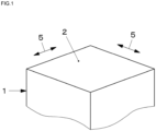
- a diamond crystal 1 is prepared as illustrated in FIG. 1 .
- the diamond crystal 1 has a bulk body, and has a main surface 2.
- the main surface 2 has a plane orientation of (100) and has ⁇ 110> directions as indicated by arrows 5 in FIG. 1 .
- the diamond crystal 1 may be a monocrystal or a polycrystal.
- the diamond crystal 1 is described as a diamond crystal having a quadrangular main surface 2, as an example exterior of the diamond crystal 1.
- the exterior of the diamond crystal 1, however, will not be limited to a quadrangular shape but may have any other shape.
- the diamond crystal 1 preferably has a thickness large enough to provide a strength that eliminates or minimizes handling inconveniences. Specifically, the diamond crystal 1 preferably has a thickness of equal to or less than 0.3 mm. Also, diamond crystals are significantly hard materials, and for considerations such as cleavability of resulting elements or devices, the upper limit of the thickness of the diamond crystal 1 is preferably equal to or less than 3.0 mm.
- the method of growing the diamond crystal 1 may be any method that is based on hetero-epitaxial growth or homo-epitaxial growth using, for example, chemical vapor deposition (CVD). From among diamond crystals that have been thus grown and formed, a diamond crystal having a main surface having a plane orientation of (100) may be prepared.
- CVD chemical vapor deposition
- polishing wheel 3 and polishing agents may be commercially available products.
- FIG. 2 Two representative contact positions (4a and 4b) are illustrated in FIG. 2 .
- the rotation direction in which the polishing wheel 3 rotates is indicated by arrow 3a in FIGs. 2 and 3 .
- a tangent extends in a tangent direction 4a 1 and contacts a curve extending in the rotation direction 3a at the contact position 4a.
- a tangent extends in a tangent direction 4b1 and contacts the curve at the contact position 4b.
- the tangent directions 4a1 and 4b1 are set within a range of ⁇ 10° relative to a ⁇ 110> direction of the diamond crystal 1 (the directions indicated by the arrows 5 in FIGs. 1 to 3 ). It is to be noted that the limitation "within a range of ⁇ 10°" encompasses ⁇ 0°.
- the angles, ⁇ that the tangent directions 4a 1 and 4b1 form with the respective ⁇ 110> directions 5 of the diamond crystal 1 are ⁇ 0° (that is, the tangent directions 4a1 and 4b1 are parallel to the respective ⁇ 110> directions 5). For this reason, illustration of the leading symbol ⁇ is omitted in FIG. 3 .
- the polishing wheel 3 is moved relative to the main surface 2 while kept in contact the main surface 2 at such contact positions that the angles ⁇ , which the tangent directions 4a1 and 4b1 form with the respective ⁇ 110> directions 5, are within a range of ⁇ 10°. Specifically, the polishing wheel 3 is moved while kept in contact with the entire area of the main surface 2 such that the angle ⁇ falls within a range of ⁇ 10° at least once at each of the contact positions with the polishing wheel 3 included in the entire area of the main surface 2.
- the principle behind how the affected region 1a appears in a direction parallel to the direction of the orientation (111) is known.
- the Applicant established a theory that explains that the (111) direction and the direction parallel to the (111) direction may be considered as directions in which affected regions tend to appear comparatively easily when machining or processing is performed.
- the affected region 1a is considered as having appeared collectively in a direction parallel to the (111) direction by making (100) the plane orientation of the main surface 2 and by moving the polishing wheel 3 relative to the main surface 2 while making the polishing wheel 3 contact the main surface 2 such that the angle ⁇ is within a range of ⁇ 10°, as described above. It is to be noted that since the affected region 1a has been caused to appear by mechanical polishing, the affected region 1a is considered as including dislocations.
- the Applicant has reached a conclusion regarding conditions for causing an affected region 1a to appear such that the affected region 1a is parallel to the direction of the plane orientation (111) of the diamond crystal 1 and penetrates the diamond crystal 1 onto the main surface 2.
- the conditions include: that the main surface 2 has a plane orientation of (100); and that the tangent directions 4a1 and 4b1 are kept within a range of ⁇ 10° relative to the respective ⁇ 110> directions 5 of the diamond crystal 1.
- FIGs. 4 and 5 illustrate example contact positions at which the angle ⁇ keeps out of the ⁇ 10° range, never falling within a range of ⁇ 10°, even once.
- the affected regions including dislocations were not located collectively in a direction parallel to the direction of the orientation (111), and the surface roughness was not on a flat level on the atomic level.
- these affected regions were not removed quickly by CMP, described later. Further, new affected regions possibly attributed to the CMP were found to have formed. As a result, it was confirmed that the affected regions on the main surface 2 are not completely removed.
- FIGs. 4 and 5 illustrate example contact positions at which the angle ⁇ relative to the ⁇ 110> direction 5 is ⁇ 45°.
- FIG. 7 illustrates the diamond crystal 1 with the affected region removed by the CMP.
- a polishing agent is used, which may be a commercially available product, exampling including zinc oxide, chromium oxide, cerium oxide, titanium oxide, ferric oxide, and silica. Also, a polishing pad is used in the CMP and may be a commercially available product.
- the principle behind how the affected region 1a was removed by the CMP is known.
- the Applicant however, established a theory that explains that the affected region 1a is removed quickly before new affected regions are formed by the CMP, making the affected regions on the main surface 2, including the affected region, 1a, removable completely by the CMP.
- a theory has been established explaining that the (111) direction of the diamond crystal 1 and a direction parallel to the (111) direction are plane directions in which affected regions tend to appear comparatively easily when machining or processing is performed.
- the affected region 1a is also subject to alteration under the CMP, which is possibly why the affected region 1a was removed quickly before new affected regions are formed by the CMP.
- the method according to the present invention and this embodiment for polishing the diamond crystal 1 and the diamond crystal 1 according to the present invention and this embodiment cause, purposefully by mechanical polishing, the affected region 1a to appear such that the affected region 1a is parallel to the direction of the plane orientation (111) of the diamond crystal 1 and penetrates the diamond crystal 1 onto the main surface 2.
- the affected region 1a By causing the affected region 1a to temporarily appear collectively in a direction parallel to the direction of the plane orientation (111) of the diamond crystal 1, affected regions including the affected region 1a are removed completely by the CMP, which is performed after the mechanical polishing.
- a method for polishing the diamond crystal 1 is realized such that the method eliminates the affected region 1a including dislocations from the main surface 2 of the diamond crystal 1.
- such a diamond crystal 1 was realized that: the main surface 2 has a plane orientation of (100); no affected region 1a is contained in a direction parallel to the direction of the orientation (111); and the affected region 1a is removed from, and thus does not appear on, the main surface 2. It is to be noted that synchrotron x-ray topography, for example, may be used to check if the affected region 1a is present or absent.
- the diamond crystal 1 prepared by the polishing method according to the present invention when used in a semiconductor application, no affected regions 1a appear on the main surface 2. This eliminates or minimizes dislocations in the semiconductor layer formed on the main surface 2 and introduction of defects. This ensures that a diamond crystal 1 capable of improving semiconductor layer properties is provided.
- the surface roughness Rq of the main surface 2 is kept at equal to or less than 5 nm by performing CMP.
- Rq may be measured using a surface roughness measuring device.
- a diamond crystal whose main surface has a surface roughness Rq of equal to or less than 5 nm is obtained. This ensures that a diamond crystal usable as a growth foundation crystal for semiconductor layers is realized.
- a diamond polycrystal was prepared by hetero-epitaxial growth.
- the diamond crystal had: a bulk body; a main surface having a plane orientation of (100); and ⁇ 110> directions indicated by the arrows 5 in FIG. 1 .
- the main surface had a quadrangular outer shape of 10 mm by 10 mm.
- the tangent direction of a tangent on a curve extending in the rotation direction of the polishing wheel was set within a range of ⁇ 10° relative to the ⁇ 110> direction of the diamond crystal.
- FIG. 8 shows a topography picture of a side surface of the diamond crystal obtained in the synchrotron x-ray topography.
- a plurality of affected regions 1a were observed each extending from the main surface in a left diagonal direction and having an approximately uniform thickness. Specifically, the affected regions 1a appeared collectively in a direction parallel to the direction of the plane orientation (111) of the diamond crystal, and penetrated the diamond crystal onto the main surface.
- FIG. 9 shows a topography picture of a side surface of the diamond crystal obtained in the synchrotron x-ray topography. As shown in FIG. 9 , it was observed that the plurality of affected regions 1a had been removed from the main surface and areas near the main surface.
Landscapes
- Chemical & Material Sciences (AREA)
- Engineering & Computer Science (AREA)
- Organic Chemistry (AREA)
- Mechanical Engineering (AREA)
- Inorganic Chemistry (AREA)
- Crystallography & Structural Chemistry (AREA)
- Metallurgy (AREA)
- Materials Engineering (AREA)
- Ceramic Engineering (AREA)
- Life Sciences & Earth Sciences (AREA)
- Geology (AREA)
- General Life Sciences & Earth Sciences (AREA)
- Crystals, And After-Treatments Of Crystals (AREA)
- Mechanical Treatment Of Semiconductor (AREA)
- Grinding And Polishing Of Tertiary Curved Surfaces And Surfaces With Complex Shapes (AREA)
- Finish Polishing, Edge Sharpening, And Grinding By Specific Grinding Devices (AREA)
- Carbon And Carbon Compounds (AREA)
- Grinding Of Cylindrical And Plane Surfaces (AREA)
Claims (4)
- Procédé de polissage d'un cristal de diamant (1), le procédé comprenant :la préparation d'un cristal de diamant (1) qui présente une surface principale (2) à orientation de plan de (100) conformément aux indices de Miller,la réalisation d'un polissage mécanique sur la surface principale (2) du cristal de diamant (1) en utilisant un disque à polir (3) qui tourne dans un sens de rotation (3a) de telle sorte que :le cristal de diamant (1) contacte le disque à polir (3) à des positions de contact (4a, 4b) sur une courbe qui s'étend dans le sens de rotation (3a) du disque à polir (3),une tangente contactant la courbe qui s'étend dans le sens de rotation (3a) du disque à polir (3) à chaque position de contact (4a, 4b), etla tangente présentant un sens de tangente (4a1, 4b1) à chaque position de contact (4a, 4b) dans une plage de ± 10 degrés par rapport à un sens de <110> du cristal de diamant (1) conformément aux indices de Miller,le disque à polir (3) étant déplacé par rapport à la surface principale (2) tout en étant maintenu en contact avec l'aire entière de la surface principale (2), de sorte que l'angle formé entre les sens de tangente (4a1, 4b1) et le sens de <110> du cristal de diamant (1) conformément aux indices de Miller à chaque position de contact avec le disque à polir (3) est compris dans la plage définie de ±10°,amenant ainsi des zones affectées (1a) à apparaître de telle sorte que les zones affectées (1a) son parallèles à un sens d'une orientation de plan (111) du cristal de diamant (1) et pénètrent dans le cristal de diamant (1) sur la surface principale (2), les zones affectées (1a) comprenant des dislocations, etla réalisation d'un polissage chimicomécanique sur la surface principale (2) du cristal de diamant (1) pour éliminer les zones affectées (1a) parallèlement au sens de l'orientation de plan (111), éliminant ainsi les zones affectées (1a) de la surface principale (2).
- Procédé de polissage d'un cristal de diamant (1) selon la revendication 1, l'étape de réalisation du polissage chimicomécanique comprenant la génération d'une rugosité de surface Rq de la surface principale (2) égale ou inférieure à 5 nm.
- Cristal de diamant (1) préparé au moyen du procédé selon la revendication 1 ou 2 et présentant une surface principale (2) à orientation de plan de (100),
aucune zone affectée n'étant contenue dans le cristal de diamant (1) parallèlement à un sens d'une orientation (111) du cristal de diamant (1), et aucune zone affectée n'apparaissant sur la surface principale (2) du cristal de diamant (1). - Cristal de diamant (1) selon la revendication 3, la surface principale (2) présentant une rugosité de surface Rq égale ou inférieure à 5 nm.
Applications Claiming Priority (2)
| Application Number | Priority Date | Filing Date | Title |
|---|---|---|---|
| JP2018048664 | 2018-03-16 | ||
| PCT/JP2019/010524 WO2019177092A1 (fr) | 2018-03-16 | 2019-03-14 | Procédé de polissage de cristal de diamant et cristal de diamant |
Publications (3)
| Publication Number | Publication Date |
|---|---|
| EP3766634A1 EP3766634A1 (fr) | 2021-01-20 |
| EP3766634A4 EP3766634A4 (fr) | 2021-12-29 |
| EP3766634B1 true EP3766634B1 (fr) | 2024-08-07 |
Family
ID=67908382
Family Applications (1)
| Application Number | Title | Priority Date | Filing Date |
|---|---|---|---|
| EP19768491.3A Active EP3766634B1 (fr) | 2018-03-16 | 2019-03-14 | Procédé de polissage de cristal de diamant et cristal de diamant |
Country Status (6)
| Country | Link |
|---|---|
| US (2) | US12134161B2 (fr) |
| EP (1) | EP3766634B1 (fr) |
| JP (1) | JPWO2019177092A1 (fr) |
| KR (1) | KR102313832B1 (fr) |
| CN (1) | CN110769975B (fr) |
| WO (1) | WO2019177092A1 (fr) |
Family Cites Families (20)
| Publication number | Priority date | Publication date | Assignee | Title |
|---|---|---|---|---|
| US1213164A (en) * | 1912-07-10 | 1917-01-23 | Gerrit A De Graaf | Method of polishing diamonds. |
| US1727425A (en) * | 1921-08-05 | 1929-09-10 | Joyce Koebel Diamond Tool Depa | Method of grinding or polishing diamonds |
| US3568368A (en) * | 1968-06-03 | 1971-03-09 | Efraim Gwircman | Continuous diamond girdle polishing machine |
| GB9109496D0 (en) * | 1990-05-04 | 1991-06-26 | Brilcut Patent | Working gemstones |
| JP3152994B2 (ja) * | 1991-04-26 | 2001-04-03 | 新日本製鐵株式会社 | ダイヤモンド結晶の成長方法 |
| JP4145437B2 (ja) * | 1999-09-28 | 2008-09-03 | 住友電気工業株式会社 | 単結晶GaNの結晶成長方法及び単結晶GaN基板の製造方法と単結晶GaN基板 |
| JP4385764B2 (ja) * | 2003-12-26 | 2009-12-16 | 住友電気工業株式会社 | ダイヤモンド単結晶基板の製造方法 |
| DE602006021467D1 (de) * | 2005-12-09 | 2011-06-01 | Element Six Technologies Pty Ltd | Synthetischer diamant mit hoher kristalliner qualität |
| US9133566B2 (en) * | 2005-12-09 | 2015-09-15 | Element Six Technologies Limited | High crystalline quality synthetic diamond |
| JP2010058204A (ja) * | 2008-09-02 | 2010-03-18 | Osg Corp | 単結晶ダイヤモンドのラップ研磨装置 |
| ES2814225T3 (es) * | 2008-09-16 | 2021-03-26 | Diamond Innovations Inc | Partículas abrasivas que tienen una morfología única |
| DE202011111028U1 (de) * | 2010-08-19 | 2018-07-03 | Sumitomo Electric Industries, Ltd. | Polykristalliner Diamant |
| GB201107730D0 (en) * | 2011-05-10 | 2011-06-22 | Element Six Ltd | Diamond sensors, detectors and quantum devices |
| WO2013187510A1 (fr) * | 2012-06-15 | 2013-12-19 | 株式会社東京精密 | Dispositif et procédé de découpage en dés |
| US9259818B2 (en) * | 2012-11-06 | 2016-02-16 | Sinmat, Inc. | Smooth diamond surfaces and CMP method for forming |
| EP3054036B1 (fr) | 2013-09-30 | 2021-03-03 | Adamant Namiki Precision Jewel Co., Ltd. | Procédé de fabrication d'un substrat en diamant |
| JP6547100B2 (ja) * | 2014-02-25 | 2019-07-24 | 国立大学法人九州大学 | 複合加工装置並びに該装置により加工された加工物 |
| JP6582597B2 (ja) * | 2015-06-19 | 2019-10-02 | 住友電気工業株式会社 | ダイヤモンド単結晶、工具およびダイヤモンド単結晶の製造方法 |
| CN107457616B (zh) * | 2017-09-07 | 2019-07-26 | 哈尔滨工业大学 | 一种基于纳米镍粉的金刚石晶体表面机械化学抛光方法 |
| CN112676999A (zh) * | 2020-12-30 | 2021-04-20 | 华侨大学 | 金刚石磨抛一体化的加工设备及其加工方法 |
-
2019
- 2019-03-14 EP EP19768491.3A patent/EP3766634B1/fr active Active
- 2019-03-14 JP JP2020506642A patent/JPWO2019177092A1/ja active Pending
- 2019-03-14 KR KR1020197036744A patent/KR102313832B1/ko active Active
- 2019-03-14 CN CN201980002973.XA patent/CN110769975B/zh active Active
- 2019-03-14 WO PCT/JP2019/010524 patent/WO2019177092A1/fr not_active Ceased
-
2020
- 2020-09-10 US US17/017,220 patent/US12134161B2/en active Active
-
2024
- 2024-09-30 US US18/901,902 patent/US20250018524A1/en active Pending
Also Published As
| Publication number | Publication date |
|---|---|
| WO2019177092A1 (fr) | 2019-09-19 |
| JPWO2019177092A1 (ja) | 2021-03-25 |
| US20200406420A1 (en) | 2020-12-31 |
| KR102313832B1 (ko) | 2021-10-15 |
| CN110769975B (zh) | 2022-04-08 |
| CN110769975A (zh) | 2020-02-07 |
| US12134161B2 (en) | 2024-11-05 |
| KR20200004410A (ko) | 2020-01-13 |
| EP3766634A4 (fr) | 2021-12-29 |
| US20250018524A1 (en) | 2025-01-16 |
| EP3766634A1 (fr) | 2021-01-20 |
Similar Documents
| Publication | Publication Date | Title |
|---|---|---|
| JP6315579B2 (ja) | SiCエピタキシャルウェハの製造方法 | |
| KR101436482B1 (ko) | 반도체 웨이퍼 및 그 제조 방법 | |
| US9318563B2 (en) | Silicon carbide single-crystal substrate | |
| KR101605384B1 (ko) | 양두 연삭 장치 및 웨이퍼의 제조 방법 | |
| CN110660840A (zh) | 碳化硅单晶衬底及用于制造所述碳化硅单晶衬底的方法 | |
| JP6013410B2 (ja) | Ga2O3系単結晶基板 | |
| EP3766634B1 (fr) | Procédé de polissage de cristal de diamant et cristal de diamant | |
| WO2012176755A1 (fr) | Procédé de fabrication d'un substrat de carbure de silicium | |
| WO2004101867A1 (fr) | Plaquette de silicium epitaxial et procede de production de ladite plaquette de silicium epitaxial | |
| US11505878B2 (en) | Diamond crystal substrate, method for producing diamond crystal substrate, and method for homo-epitaxially growing diamond crystal | |
| KR101267982B1 (ko) | 반도체 기판의 연마방법 및 반도체 기판의 연마장치 | |
| JP6149988B2 (ja) | 炭化珪素単結晶基板 | |
| JP2016007690A (ja) | サファイア基板の製造方法 | |
| EP3098839B1 (fr) | Procédé de transfert d'une couche d'un substrat monocristallin | |
| JP6347354B2 (ja) | Ramo4基板 | |
| CN120674302A (zh) | 金刚石衬底加工方法 | |
| JP2016037418A (ja) | Ga2O3系単結晶基板 |
Legal Events
| Date | Code | Title | Description |
|---|---|---|---|
| STAA | Information on the status of an ep patent application or granted ep patent |
Free format text: STATUS: THE INTERNATIONAL PUBLICATION HAS BEEN MADE |
|
| PUAI | Public reference made under article 153(3) epc to a published international application that has entered the european phase |
Free format text: ORIGINAL CODE: 0009012 |
|
| STAA | Information on the status of an ep patent application or granted ep patent |
Free format text: STATUS: REQUEST FOR EXAMINATION WAS MADE |
|
| 17P | Request for examination filed |
Effective date: 20201012 |
|
| AK | Designated contracting states |
Kind code of ref document: A1 Designated state(s): AL AT BE BG CH CY CZ DE DK EE ES FI FR GB GR HR HU IE IS IT LI LT LU LV MC MK MT NL NO PL PT RO RS SE SI SK SM TR |
|
| AX | Request for extension of the european patent |
Extension state: BA ME |
|
| DAV | Request for validation of the european patent (deleted) | ||
| DAX | Request for extension of the european patent (deleted) | ||
| A4 | Supplementary search report drawn up and despatched |
Effective date: 20211126 |
|
| RIC1 | Information provided on ipc code assigned before grant |
Ipc: H01L 21/304 20060101ALI20211122BHEP Ipc: H01L 21/306 20060101ALI20211122BHEP Ipc: C30B 33/00 20060101ALI20211122BHEP Ipc: C30B 29/04 20060101ALI20211122BHEP Ipc: C01B 32/28 20170101ALI20211122BHEP Ipc: B24B 37/10 20120101ALI20211122BHEP Ipc: B24B 7/22 20060101ALI20211122BHEP Ipc: B24B 1/00 20060101AFI20211122BHEP |
|
| STAA | Information on the status of an ep patent application or granted ep patent |
Free format text: STATUS: EXAMINATION IS IN PROGRESS |
|
| 17Q | First examination report despatched |
Effective date: 20230210 |
|
| RAP3 | Party data changed (applicant data changed or rights of an application transferred) |
Owner name: ORBRAY CO., LTD. |
|
| GRAP | Despatch of communication of intention to grant a patent |
Free format text: ORIGINAL CODE: EPIDOSNIGR1 |
|
| STAA | Information on the status of an ep patent application or granted ep patent |
Free format text: STATUS: GRANT OF PATENT IS INTENDED |
|
| GRAJ | Information related to disapproval of communication of intention to grant by the applicant or resumption of examination proceedings by the epo deleted |
Free format text: ORIGINAL CODE: EPIDOSDIGR1 |
|
| STAA | Information on the status of an ep patent application or granted ep patent |
Free format text: STATUS: EXAMINATION IS IN PROGRESS |
|
| INTG | Intention to grant announced |
Effective date: 20240109 |
|
| INTC | Intention to grant announced (deleted) | ||
| GRAP | Despatch of communication of intention to grant a patent |
Free format text: ORIGINAL CODE: EPIDOSNIGR1 |
|
| STAA | Information on the status of an ep patent application or granted ep patent |
Free format text: STATUS: GRANT OF PATENT IS INTENDED |
|
| INTG | Intention to grant announced |
Effective date: 20240314 |
|
| P01 | Opt-out of the competence of the unified patent court (upc) registered |
Effective date: 20240417 |
|
| GRAS | Grant fee paid |
Free format text: ORIGINAL CODE: EPIDOSNIGR3 |
|
| GRAA | (expected) grant |
Free format text: ORIGINAL CODE: 0009210 |
|
| STAA | Information on the status of an ep patent application or granted ep patent |
Free format text: STATUS: THE PATENT HAS BEEN GRANTED |
|
| AK | Designated contracting states |
Kind code of ref document: B1 Designated state(s): AL AT BE BG CH CY CZ DE DK EE ES FI FR GB GR HR HU IE IS IT LI LT LU LV MC MK MT NL NO PL PT RO RS SE SI SK SM TR |
|
| REG | Reference to a national code |
Ref country code: GB Ref legal event code: FG4D |
|
| REG | Reference to a national code |
Ref country code: CH Ref legal event code: EP |
|
| REG | Reference to a national code |
Ref country code: IE Ref legal event code: FG4D |
|
| REG | Reference to a national code |
Ref country code: DE Ref legal event code: R096 Ref document number: 602019056617 Country of ref document: DE |
|
| REG | Reference to a national code |
Ref country code: LT Ref legal event code: MG9D |
|
| REG | Reference to a national code |
Ref country code: NL Ref legal event code: MP Effective date: 20240807 |
|
| PG25 | Lapsed in a contracting state [announced via postgrant information from national office to epo] |
Ref country code: NO Free format text: LAPSE BECAUSE OF FAILURE TO SUBMIT A TRANSLATION OF THE DESCRIPTION OR TO PAY THE FEE WITHIN THE PRESCRIBED TIME-LIMIT Effective date: 20241107 |
|
| REG | Reference to a national code |
Ref country code: AT Ref legal event code: MK05 Ref document number: 1710418 Country of ref document: AT Kind code of ref document: T Effective date: 20240807 |
|
| PG25 | Lapsed in a contracting state [announced via postgrant information from national office to epo] |
Ref country code: FI Free format text: LAPSE BECAUSE OF FAILURE TO SUBMIT A TRANSLATION OF THE DESCRIPTION OR TO PAY THE FEE WITHIN THE PRESCRIBED TIME-LIMIT Effective date: 20240807 Ref country code: NL Free format text: LAPSE BECAUSE OF FAILURE TO SUBMIT A TRANSLATION OF THE DESCRIPTION OR TO PAY THE FEE WITHIN THE PRESCRIBED TIME-LIMIT Effective date: 20240807 Ref country code: PL Free format text: LAPSE BECAUSE OF FAILURE TO SUBMIT A TRANSLATION OF THE DESCRIPTION OR TO PAY THE FEE WITHIN THE PRESCRIBED TIME-LIMIT Effective date: 20240807 Ref country code: PT Free format text: LAPSE BECAUSE OF FAILURE TO SUBMIT A TRANSLATION OF THE DESCRIPTION OR TO PAY THE FEE WITHIN THE PRESCRIBED TIME-LIMIT Effective date: 20241209 Ref country code: GR Free format text: LAPSE BECAUSE OF FAILURE TO SUBMIT A TRANSLATION OF THE DESCRIPTION OR TO PAY THE FEE WITHIN THE PRESCRIBED TIME-LIMIT Effective date: 20241108 |
|
| PG25 | Lapsed in a contracting state [announced via postgrant information from national office to epo] |
Ref country code: BG Free format text: LAPSE BECAUSE OF FAILURE TO SUBMIT A TRANSLATION OF THE DESCRIPTION OR TO PAY THE FEE WITHIN THE PRESCRIBED TIME-LIMIT Effective date: 20240807 |
|
| PG25 | Lapsed in a contracting state [announced via postgrant information from national office to epo] |
Ref country code: LV Free format text: LAPSE BECAUSE OF FAILURE TO SUBMIT A TRANSLATION OF THE DESCRIPTION OR TO PAY THE FEE WITHIN THE PRESCRIBED TIME-LIMIT Effective date: 20240807 |
|
| PG25 | Lapsed in a contracting state [announced via postgrant information from national office to epo] |
Ref country code: AT Free format text: LAPSE BECAUSE OF FAILURE TO SUBMIT A TRANSLATION OF THE DESCRIPTION OR TO PAY THE FEE WITHIN THE PRESCRIBED TIME-LIMIT Effective date: 20240807 Ref country code: IS Free format text: LAPSE BECAUSE OF FAILURE TO SUBMIT A TRANSLATION OF THE DESCRIPTION OR TO PAY THE FEE WITHIN THE PRESCRIBED TIME-LIMIT Effective date: 20241207 |
|
| PG25 | Lapsed in a contracting state [announced via postgrant information from national office to epo] |
Ref country code: HR Free format text: LAPSE BECAUSE OF FAILURE TO SUBMIT A TRANSLATION OF THE DESCRIPTION OR TO PAY THE FEE WITHIN THE PRESCRIBED TIME-LIMIT Effective date: 20240807 |
|
| PG25 | Lapsed in a contracting state [announced via postgrant information from national office to epo] |
Ref country code: ES Free format text: LAPSE BECAUSE OF FAILURE TO SUBMIT A TRANSLATION OF THE DESCRIPTION OR TO PAY THE FEE WITHIN THE PRESCRIBED TIME-LIMIT Effective date: 20240807 Ref country code: RS Free format text: LAPSE BECAUSE OF FAILURE TO SUBMIT A TRANSLATION OF THE DESCRIPTION OR TO PAY THE FEE WITHIN THE PRESCRIBED TIME-LIMIT Effective date: 20241107 |
|
| PG25 | Lapsed in a contracting state [announced via postgrant information from national office to epo] |
Ref country code: RS Free format text: LAPSE BECAUSE OF FAILURE TO SUBMIT A TRANSLATION OF THE DESCRIPTION OR TO PAY THE FEE WITHIN THE PRESCRIBED TIME-LIMIT Effective date: 20241107 Ref country code: PT Free format text: LAPSE BECAUSE OF FAILURE TO SUBMIT A TRANSLATION OF THE DESCRIPTION OR TO PAY THE FEE WITHIN THE PRESCRIBED TIME-LIMIT Effective date: 20241209 Ref country code: PL Free format text: LAPSE BECAUSE OF FAILURE TO SUBMIT A TRANSLATION OF THE DESCRIPTION OR TO PAY THE FEE WITHIN THE PRESCRIBED TIME-LIMIT Effective date: 20240807 Ref country code: NO Free format text: LAPSE BECAUSE OF FAILURE TO SUBMIT A TRANSLATION OF THE DESCRIPTION OR TO PAY THE FEE WITHIN THE PRESCRIBED TIME-LIMIT Effective date: 20241107 Ref country code: NL Free format text: LAPSE BECAUSE OF FAILURE TO SUBMIT A TRANSLATION OF THE DESCRIPTION OR TO PAY THE FEE WITHIN THE PRESCRIBED TIME-LIMIT Effective date: 20240807 Ref country code: LV Free format text: LAPSE BECAUSE OF FAILURE TO SUBMIT A TRANSLATION OF THE DESCRIPTION OR TO PAY THE FEE WITHIN THE PRESCRIBED TIME-LIMIT Effective date: 20240807 Ref country code: IS Free format text: LAPSE BECAUSE OF FAILURE TO SUBMIT A TRANSLATION OF THE DESCRIPTION OR TO PAY THE FEE WITHIN THE PRESCRIBED TIME-LIMIT Effective date: 20241207 Ref country code: HR Free format text: LAPSE BECAUSE OF FAILURE TO SUBMIT A TRANSLATION OF THE DESCRIPTION OR TO PAY THE FEE WITHIN THE PRESCRIBED TIME-LIMIT Effective date: 20240807 Ref country code: GR Free format text: LAPSE BECAUSE OF FAILURE TO SUBMIT A TRANSLATION OF THE DESCRIPTION OR TO PAY THE FEE WITHIN THE PRESCRIBED TIME-LIMIT Effective date: 20241108 Ref country code: FI Free format text: LAPSE BECAUSE OF FAILURE TO SUBMIT A TRANSLATION OF THE DESCRIPTION OR TO PAY THE FEE WITHIN THE PRESCRIBED TIME-LIMIT Effective date: 20240807 Ref country code: ES Free format text: LAPSE BECAUSE OF FAILURE TO SUBMIT A TRANSLATION OF THE DESCRIPTION OR TO PAY THE FEE WITHIN THE PRESCRIBED TIME-LIMIT Effective date: 20240807 Ref country code: BG Free format text: LAPSE BECAUSE OF FAILURE TO SUBMIT A TRANSLATION OF THE DESCRIPTION OR TO PAY THE FEE WITHIN THE PRESCRIBED TIME-LIMIT Effective date: 20240807 Ref country code: AT Free format text: LAPSE BECAUSE OF FAILURE TO SUBMIT A TRANSLATION OF THE DESCRIPTION OR TO PAY THE FEE WITHIN THE PRESCRIBED TIME-LIMIT Effective date: 20240807 |
|
| PG25 | Lapsed in a contracting state [announced via postgrant information from national office to epo] |
Ref country code: DK Free format text: LAPSE BECAUSE OF FAILURE TO SUBMIT A TRANSLATION OF THE DESCRIPTION OR TO PAY THE FEE WITHIN THE PRESCRIBED TIME-LIMIT Effective date: 20240807 Ref country code: SM Free format text: LAPSE BECAUSE OF FAILURE TO SUBMIT A TRANSLATION OF THE DESCRIPTION OR TO PAY THE FEE WITHIN THE PRESCRIBED TIME-LIMIT Effective date: 20240807 Ref country code: RO Free format text: LAPSE BECAUSE OF FAILURE TO SUBMIT A TRANSLATION OF THE DESCRIPTION OR TO PAY THE FEE WITHIN THE PRESCRIBED TIME-LIMIT Effective date: 20240807 |
|
| PG25 | Lapsed in a contracting state [announced via postgrant information from national office to epo] |
Ref country code: EE Free format text: LAPSE BECAUSE OF FAILURE TO SUBMIT A TRANSLATION OF THE DESCRIPTION OR TO PAY THE FEE WITHIN THE PRESCRIBED TIME-LIMIT Effective date: 20240807 |
|
| PG25 | Lapsed in a contracting state [announced via postgrant information from national office to epo] |
Ref country code: CZ Free format text: LAPSE BECAUSE OF FAILURE TO SUBMIT A TRANSLATION OF THE DESCRIPTION OR TO PAY THE FEE WITHIN THE PRESCRIBED TIME-LIMIT Effective date: 20240807 |
|
| PG25 | Lapsed in a contracting state [announced via postgrant information from national office to epo] |
Ref country code: SK Free format text: LAPSE BECAUSE OF FAILURE TO SUBMIT A TRANSLATION OF THE DESCRIPTION OR TO PAY THE FEE WITHIN THE PRESCRIBED TIME-LIMIT Effective date: 20240807 |
|
| REG | Reference to a national code |
Ref country code: DE Ref legal event code: R097 Ref document number: 602019056617 Country of ref document: DE |
|
| PLBE | No opposition filed within time limit |
Free format text: ORIGINAL CODE: 0009261 |
|
| STAA | Information on the status of an ep patent application or granted ep patent |
Free format text: STATUS: NO OPPOSITION FILED WITHIN TIME LIMIT |
|
| 26N | No opposition filed |
Effective date: 20250508 |
|
| PG25 | Lapsed in a contracting state [announced via postgrant information from national office to epo] |
Ref country code: SE Free format text: LAPSE BECAUSE OF FAILURE TO SUBMIT A TRANSLATION OF THE DESCRIPTION OR TO PAY THE FEE WITHIN THE PRESCRIBED TIME-LIMIT Effective date: 20240807 |
|
| PG25 | Lapsed in a contracting state [announced via postgrant information from national office to epo] |
Ref country code: MC Free format text: LAPSE BECAUSE OF FAILURE TO SUBMIT A TRANSLATION OF THE DESCRIPTION OR TO PAY THE FEE WITHIN THE PRESCRIBED TIME-LIMIT Effective date: 20240807 |
|
| REG | Reference to a national code |
Ref country code: CH Ref legal event code: H13 Free format text: ST27 STATUS EVENT CODE: U-0-0-H10-H13 (AS PROVIDED BY THE NATIONAL OFFICE) Effective date: 20251023 |
|
| PG25 | Lapsed in a contracting state [announced via postgrant information from national office to epo] |
Ref country code: LU Free format text: LAPSE BECAUSE OF NON-PAYMENT OF DUE FEES Effective date: 20250314 |
|
| REG | Reference to a national code |
Ref country code: BE Ref legal event code: MM Effective date: 20250331 |
|
| PG25 | Lapsed in a contracting state [announced via postgrant information from national office to epo] |
Ref country code: BE Free format text: LAPSE BECAUSE OF NON-PAYMENT OF DUE FEES Effective date: 20250331 |
|
| PG25 | Lapsed in a contracting state [announced via postgrant information from national office to epo] |
Ref country code: CH Free format text: LAPSE BECAUSE OF NON-PAYMENT OF DUE FEES Effective date: 20250331 |
|
| PG25 | Lapsed in a contracting state [announced via postgrant information from national office to epo] |
Ref country code: IE Free format text: LAPSE BECAUSE OF NON-PAYMENT OF DUE FEES Effective date: 20250314 |
|
| PG25 | Lapsed in a contracting state [announced via postgrant information from national office to epo] |
Ref country code: IT Free format text: LAPSE BECAUSE OF FAILURE TO SUBMIT A TRANSLATION OF THE DESCRIPTION OR TO PAY THE FEE WITHIN THE PRESCRIBED TIME-LIMIT Effective date: 20240807 |
|
| PGFP | Annual fee paid to national office [announced via postgrant information from national office to epo] |
Ref country code: GB Payment date: 20260324 Year of fee payment: 8 |
|
| PGFP | Annual fee paid to national office [announced via postgrant information from national office to epo] |
Ref country code: DE Payment date: 20260319 Year of fee payment: 8 |
|
| PGFP | Annual fee paid to national office [announced via postgrant information from national office to epo] |
Ref country code: FR Payment date: 20260323 Year of fee payment: 8 |