EP3767352B1 - Optische multiplexer-schaltung - Google Patents
Optische multiplexer-schaltung Download PDFInfo
- Publication number
- EP3767352B1 EP3767352B1 EP20175143.5A EP20175143A EP3767352B1 EP 3767352 B1 EP3767352 B1 EP 3767352B1 EP 20175143 A EP20175143 A EP 20175143A EP 3767352 B1 EP3767352 B1 EP 3767352B1
- Authority
- EP
- European Patent Office
- Prior art keywords
- waveguide
- light beam
- optical waveguide
- order mode
- optical
- Prior art date
- Legal status (The legal status is an assumption and is not a legal conclusion. Google has not performed a legal analysis and makes no representation as to the accuracy of the status listed.)
- Active
Links
Images


Classifications
-
- G—PHYSICS
- G02—OPTICS
- G02B—OPTICAL ELEMENTS, SYSTEMS OR APPARATUS
- G02B6/00—Light guides; Structural details of arrangements comprising light guides and other optical elements, e.g. couplings
- G02B6/24—Coupling light guides
- G02B6/26—Optical coupling means
- G02B6/28—Optical coupling means having data bus means, i.e. plural waveguides interconnected and providing an inherently bidirectional system by mixing and splitting signals
- G02B6/293—Optical coupling means having data bus means, i.e. plural waveguides interconnected and providing an inherently bidirectional system by mixing and splitting signals with wavelength selective means
- G02B6/29344—Optical coupling means having data bus means, i.e. plural waveguides interconnected and providing an inherently bidirectional system by mixing and splitting signals with wavelength selective means operating by modal interference or beating, i.e. of transverse modes, e.g. zero-gap directional coupler, MMI
-
- G—PHYSICS
- G02—OPTICS
- G02B—OPTICAL ELEMENTS, SYSTEMS OR APPARATUS
- G02B6/00—Light guides; Structural details of arrangements comprising light guides and other optical elements, e.g. couplings
- G02B6/10—Light guides; Structural details of arrangements comprising light guides and other optical elements, e.g. couplings of the optical waveguide type
- G02B6/12—Light guides; Structural details of arrangements comprising light guides and other optical elements, e.g. couplings of the optical waveguide type of the integrated circuit kind
- G02B6/12007—Light guides; Structural details of arrangements comprising light guides and other optical elements, e.g. couplings of the optical waveguide type of the integrated circuit kind forming wavelength selective elements, e.g. multiplexer, demultiplexer
-
- G—PHYSICS
- G02—OPTICS
- G02B—OPTICAL ELEMENTS, SYSTEMS OR APPARATUS
- G02B6/00—Light guides; Structural details of arrangements comprising light guides and other optical elements, e.g. couplings
- G02B6/10—Light guides; Structural details of arrangements comprising light guides and other optical elements, e.g. couplings of the optical waveguide type
- G02B6/14—Mode converters
-
- G—PHYSICS
- G02—OPTICS
- G02B—OPTICAL ELEMENTS, SYSTEMS OR APPARATUS
- G02B6/00—Light guides; Structural details of arrangements comprising light guides and other optical elements, e.g. couplings
- G02B6/24—Coupling light guides
- G02B6/26—Optical coupling means
- G02B6/28—Optical coupling means having data bus means, i.e. plural waveguides interconnected and providing an inherently bidirectional system by mixing and splitting signals
- G02B6/293—Optical coupling means having data bus means, i.e. plural waveguides interconnected and providing an inherently bidirectional system by mixing and splitting signals with wavelength selective means
- G02B6/29331—Optical coupling means having data bus means, i.e. plural waveguides interconnected and providing an inherently bidirectional system by mixing and splitting signals with wavelength selective means operating by evanescent wave coupling
- G02B6/29332—Wavelength selective couplers, i.e. based on evanescent coupling between light guides, e.g. fused fibre couplers with transverse coupling between fibres having different propagation constant wavelength dependency
-
- G—PHYSICS
- G02—OPTICS
- G02B—OPTICAL ELEMENTS, SYSTEMS OR APPARATUS
- G02B6/00—Light guides; Structural details of arrangements comprising light guides and other optical elements, e.g. couplings
- G02B6/24—Coupling light guides
- G02B6/26—Optical coupling means
- G02B6/28—Optical coupling means having data bus means, i.e. plural waveguides interconnected and providing an inherently bidirectional system by mixing and splitting signals
- G02B6/293—Optical coupling means having data bus means, i.e. plural waveguides interconnected and providing an inherently bidirectional system by mixing and splitting signals with wavelength selective means
- G02B6/29379—Optical coupling means having data bus means, i.e. plural waveguides interconnected and providing an inherently bidirectional system by mixing and splitting signals with wavelength selective means characterised by the function or use of the complete device
- G02B6/2938—Optical coupling means having data bus means, i.e. plural waveguides interconnected and providing an inherently bidirectional system by mixing and splitting signals with wavelength selective means characterised by the function or use of the complete device for multiplexing or demultiplexing, i.e. combining or separating wavelengths, e.g. 1xN, NxM
Definitions
- the present invention relates to an optical multiplexing circuit and more specifically relates to, for example, a three-primary-color optical multiplexing circuit that multiplexes visible light beams having three primary colors, namely, R, G, and B light beams (R: red light, G: green light, B: blue light).
- an RGB coupler module using a silica-based planar lightwave circuit has been drawing attention as a circuit element that multiplexes visible light beams of three primary colors for eyeglass-type devices and projectors (see Non Patent Literature 1, for example).
- PLC silica-based planar lightwave circuit
- optical waveguides are created in a planar substrate by patterning and etching processes in photolithography or the like and a plurality of basic optical circuits (e.g. directional couplers, Mach-Zehnder interferometers, etc.) are combined with each other to implement various functions.
- Non Patent Literature 1 There is a three-primary-color multiplexing circuit that utilizes, for example, directional couplers and/or Mach-Zehnder interferometers (see Non Patent Literature 1).
- directional couplers and/or Mach-Zehnder interferometers
- Fig. 1 the simplest case of using directional couplers will be described by taking Fig. 1 as an example.
- Fig. 1 illustrates the basic structure of an RGB coupler module using a PLC.
- the basic structure of the RGB coupler module using a PLC is formed of three optical waveguides, which are first to third optical waveguides 1 to 3.
- a first directional coupler 4 is coupled to the first optical waveguide 1.
- An output waveguide 5 is coupled to the second optical waveguide 2.
- a second directional coupler 6 is coupled to the third optical waveguide 3.
- the waveguide length, waveguide width, and inter-waveguide gap of the first directional coupler 4 are designed such that the first directional coupler 4 couples a light beam with a wavelength ⁇ 1 from the first optical waveguide 1 to the second optical waveguide 2, and couples a light beam with a wavelength ⁇ 2 from the second optical waveguide 2 to the first optical waveguide 1 and from the first optical waveguide 1 to the second optical waveguide 2.
- the waveguide length, waveguide width, and inter-waveguide gap of the second directional coupler 6 are designed such that the second directional coupler 6 couples a light beam with a wavelength ⁇ 3 from the third optical waveguide 3 to the second optical waveguide 2 and transmits the light beams with the wavelength ⁇ 1 and the wavelength ⁇ 2.
- a blue light beam (wavelength ⁇ 1) is input to the first optical waveguide 1
- a green light beam (wavelength ⁇ 2) is input to the second optical waveguide 2
- a red light beam (wavelength ⁇ 3) is input to the third optical waveguide 3, for example.
- the light beams of the three colors are multiplexed through the first directional coupler 4 and the second directional coupler 6 and output from the output waveguide 5.
- a three-primary-color optical multiplexing circuit deals with the wavelength of the blue light beam (wavelength band 400 nm) and the wavelength of the red light beam (wavelength band 700 nm), which greatly differ from each other. Accordingly, the wavelength dependency of the coupling length is significant. This makes it possible to make a configuration as above.
- Non Patent Literature 2 light beams with different wavelengths can be multiplexed also by using a multi-mode interference (MMI) waveguide.
- MMI multi-mode interference
- Fig. 2 illustrates the basic principle of a directional coupler.
- Fig. 2 illustrates two waveguides 11 and 12.
- the directional coupler is a coupler that transfers a light beam passing through one of the waveguides, or the waveguide 11, to the opposite waveguide 12 in a state where the two waveguides 11 and 12 are arranged close to each other.
- the light transfer ratio is 100%.
- the waveguides need to be designed to satisfy conditions for coupling the blue light beam with the wavelength ⁇ 1 propagating through the first optical waveguide 1 to the second optical waveguide 2 at the first directional coupler 4 to couple it to the green light beam with the wavelength ⁇ 2 propagating through the second optical waveguide 2.
- the waveguides also need to be designed to satisfy conditions for transmitting the light beams with the wavelengths ⁇ 1 and ⁇ 2 coupled at the second optical waveguide 2 at the second directional coupler 6 and coupling the red light beam with the wavelength ⁇ 3 propagating through the third optical waveguide 3 to the second optical waveguide 2 at the second directional coupler 6.
- a waveguide design is needed that satisfies conditions for matching between the light beam with the wavelength ⁇ 2 propagating through the second optical waveguide 2 and the light beams with the wavelengths ⁇ 1 and ⁇ 3 propagating through the first and third optical waveguides 1 and 3, respectively.
- the red light beam can be transferred with a short waveguide length by narrowing the inter-waveguide gap to a certain extent.
- the blue light with the wavelength ⁇ 1 and the green light with the wavelength ⁇ 2 are not transmitted at the second directional coupler 6 but transferred to the third optical waveguide 3. This increases the optical loss.
- the inter-waveguide gap needs to be large and the coupler length needs to be long. Doing so, however, leads to a problem that the waveguide length cannot be shortened and the optical multiplexing circuit cannot therefore be downsized.
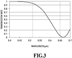
- Fig. 3 illustrates a transmission spectrum calculated via a simulation by the beam propagation method (BPM) for specific numerical values of the second directional coupler 6 illustrated in Fig. 1 .
- the waveguide length is set to 3700 ⁇ m
- the waveguide width is set to 1.5 ⁇ m
- the waveguide thickness is set to 3.6 ⁇ m
- the inter-waveguide gap is set to 4.8 ⁇ m
- a relative refractive index difference ⁇ between the core and the cladding is set to 0.45%
- ⁇ 1 is set to 450 nm (blue)
- ⁇ 2 is set to 520 nm (green)
- ⁇ 3 is set to 650 nm (red).
- BPM beam propagation method
- the second directional coupler 6 transmits 99.6% of the light beam with the wavelength ⁇ 1, transmits 93.0% of the light beam with the wavelength ⁇ 2, and couples 95.5% of the light beam with the wavelength ⁇ 3 to the second optical waveguide 2.
- the light beams with the wavelengths ⁇ 1 and ⁇ 2 are coupled to the third optical waveguide 3, thereby lowering the transmission rate.
- an input waveguide and a directional coupler may be added to add another light beam in an attempt to raise the intensity of the exiting light beam.
- the light beams originally multiplexed in the optical multiplexing circuit before the addition exit from the added input waveguide and/or directional coupler This makes it impossible to raise the intensity of the exiting light beam.
- the present invention has been made in view of the above problems, and an object thereof is to make an optical multiplexing circuit that is small and multiplexes a plurality of light beams with a plurality of wavelengths with a low loss, and also to make an optical multiplexing circuit that can output a multiplexed light beam with higher intensity and a smaller spot diameter when multiplexing a plurality of light beams with a plurality of wavelengths using a planar lightwave circuit.
- the present invention even in the case of multiplexing a plurality of light beams with a plurality of wavelengths using a PLC, if conditions for coupling the light beams with desired wavelengths are satisfied, it is possible to suppress coupling of the light beams with the other wavelengths and couple and multiplex only the light beams with the desired wavelengths. Then, the gap at each directional coupler can be narrowed within the fabrication capability, and accordingly the coupling length can be shortened. It is therefore possible to make an efficient and small optical multiplexing circuit.
- the intensity of existing light from an RGB multiplexing circuit using a planar lightwave circuit by be raised by using a space multiplexing technique.
- light beams with wavelengths ⁇ 1, ⁇ 2, and ⁇ 3 are light beams with wavelengths in blue (400 to 495 nm), green (495 to 570 nm), and red (620 to 750 nm) wavelength bands, respectively.
- Fig. 4 exemplarily illustrates the optical multiplexing circuit according to example 1 not falling under the scope of the claims.
- Fig. 4 illustrates an optical multiplexing circuit including a first optical waveguide 101 in which the light beam with the wavelength ⁇ 3 is input, a second optical waveguide 102 in which the light beams with the wavelengths ⁇ 1 and ⁇ 2 are input, a multi-mode (MM) conversion waveguide 103, a first coupling part 104, a second coupling part 105, and an output waveguide 106 coupled to the second optical waveguide 102.
- MM multi-mode
- description will be given of an example where the two light beams with the wavelengths ⁇ 1 and ⁇ 2 are input into the second optical waveguide 102.
- the configuration is not limited to this but may be such that only one of the light beams is input into the second optical waveguide 102.
- the first and second optical waveguides 101 and 102 and the MM conversion waveguide 103 are formed of a lower cladding layer provided on a substrate, a core layer higher in refractive index than the lower cladding layer, and an upper cladding layer provided on the core layer.
- the upper cladding layer is provided so as to surround the core layer.
- the first and second optical waveguides 101 and 102 can be single-mode waveguides. As illustrated in Fig. 4 , the first optical waveguide 101, the second optical waveguide 102, and the MM conversion waveguide 103 are arranged side by side along the light travel direction.
- the first and second optical waveguides 101 and 102 and the MM conversion waveguide 103 differ from each other in waveguide width.
- the first coupling part 104 is a directional coupler formed by arranging the first optical waveguide 101 and the MM conversion waveguide 103 close to each other.
- the second coupling part 105 is a directional coupler formed by arranging the second optical waveguide 102 and the MM conversion waveguide 103 close to each other.
- the MM conversion waveguide 103 is provided between the first and second optical waveguides 101 and 102.
- the light beam with the wavelength ⁇ 3 having input to the first optical waveguide 101 undergoes waveguide mode conversion into a higher order mode (e.g. first order mode) and transfers to the MM conversion waveguide 103 at the first coupling part 104.
- the light beam with the wavelength ⁇ 3 having transferred to the MM conversion waveguide 103 further undergoes waveguide mode conversion into the fundamental mode (0-th order mode) and transfers to the second optical waveguide 102 at the second coupling part 105.
- the two light beams with the wavelengths ⁇ 1 and ⁇ 2 in the 0-th order mode having input to the second optical waveguide 102 do not transfer to the MM conversion waveguide 103 at the second coupling part 105 but are transmitted by the second coupling part 105 since, as described later, the second coupling part 105 is designed not to satisfy conditions for coupling them to the MM conversion waveguide 103.
- the light beams with the wavelengths ⁇ 1 and ⁇ 2 transmitted by the second coupling part 105 and the light beam with the wavelength ⁇ 3 having transferred from the first optical waveguide 101 through the MM conversion waveguide 103 are multiplexed.
- the multiplexed light beam is output from the output waveguide 106.
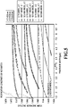
- the waveguide thickness is 3.6 ⁇ m and the relative refractive index difference ⁇ is 0.45%, which are the same conditions as those used in Fig. 3 .
- the waveguide widths of the first and second optical waveguides 101 and 102 are 1.5 ⁇ m, and the waveguide width of the MM conversion waveguide 103 is 4.8 ⁇ m.
- the effective refractive indexes of the light beam with the wavelength ⁇ 3 in the 0-th order mode and the first order mode substantially coincide with each other. This indicates that the light beam transfers between the first optical waveguide 101 and the MM conversion waveguide 103 based on (equation 2).
- the light beam with the wavelength ⁇ 3 propagating through the first optical waveguide 101 is converted into a first order mode light beam and coupled to the MM conversion waveguide 103 at the first coupling part 104 and is converted into a 0-th order light beam and coupled to the second optical waveguide 102 at the second coupling part 105.
- the second coupling part 105 can be designed by considering only the conditions for the coupling of the light beam with the wavelength ⁇ 3.
- the waveguide widths of the first and second optical waveguides 101 and 102 and the waveguide width of the MM conversion waveguide 103 may just need to be designed such that the effective refractive index of the first optical waveguide 101 with the light beam with the wavelength ⁇ 3 in the 0-th order mode is equal to the effective refractive index of the MM conversion waveguide 103 with the light beam with the wavelength ⁇ 3 in the higher order mode and that the effective refractive index of the second optical waveguide 102 with each of the light beams with the wavelengths ⁇ 1 and ⁇ 2 in the 0-th order mode is not equal to the effective refractive index of the MM conversion waveguide 103 with each of the light beams with the wavelengths ⁇ 1 and ⁇ 2 in the higher order mode.
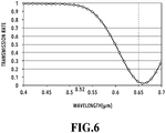
- Fig. 6 illustrates a transmission spectrum in a case where, for example, the waveguide thickness is 3.6 ⁇ m, the relative refractive index difference ⁇ is 0.45%, and inter-waveguide gaps G and waveguide lengths L illustrated in Fig. 4 are 2.5 ⁇ m and 702 ⁇ m, respectively.
- the optical multiplexing circuit according to this example 1 it is possible to shorten the waveguide length to approximately 1/5 of the waveguide length in a conventional configuration without deteriorating the characteristics.
- FIG. 7 illustrates another example of the optical multiplexing circuit according to this example 1 for the cases of multiplexing four or more light beams with mutually different wavelengths.
- the optical multiplexing circuit illustrated in Fig. 7 includes the first optical waveguide 101, the MM conversion waveguide 103, the first coupling part 104, and the second coupling part 105 and further includes one or more optical circuits 120 each including a third optical waveguide 107, a second MM conversion waveguide 108, and third and fourth coupling parts 109 and 110.
- the one or more optical circuits 120 are arranged at a plurality of stages along the light travel direction.
- the third optical waveguides 107 of the one or more optical circuits 120 receive light beams with wavelengths different from the wavelengths ⁇ 1 to ⁇ 3 and different from each other.
- the waveguide widths of the third optical waveguide 107 and the second MM conversion waveguide 108 in each of the one or more optical circuits 120 are set such that the effective refractive index of the third optical waveguide 107 with an input light beam in the 0-th order mode is equal to the effective refractive index of the second MM conversion waveguide 108 with this input light beam in a higher order mode and that the effective refractive indexes of the second MM conversion waveguide 108 with the multiplexed light beam in the higher order mode inputting the fourth coupling part 110 are not equal to the effective refractive indexes of the second optical waveguide 10 with the multiplexed light beam in the 0-th order mode inputting the fourth coupling part 110.
- light beams with mutually different wavelengths in the 0-th order mode having input to the respective third optical waveguides 107 can be converted into multi-mode light beams and transfer to the respective second MM conversion waveguides 108 at the respective third coupling parts 109, and be further converted into the fundamental mode and transfer to the second optical waveguide 102 at the respective fourth coupling parts 110.
- the light beams having transferred to the fourth coupling parts 110 are each multiplexed at the second optical waveguide 102.
- four or more light beams can be output from the output waveguide 106.
- the waveguide widths and refractive indexes of the first and second optical waveguides 101 and 102 and the MM conversion waveguide 103 are comparative.
- the waveguide widths of the first and second optical waveguides 101 and 102 may be adjusted such that the propagation constants of the light beams in the 0-th order mode with the waveguide widths of the first and second optical waveguides 101 and 102 are equal to the propagation constant of the light beam in the higher order mode with the waveguide width of the MM conversion waveguide 103.
- FIG. 8 is a diagram exemplarily illustrating the optical multiplexing circuit according to the example not falling under the scope of the claims.
- Fig. 8 illustrates an optical multiplexing circuit including first to third waveguides 201 to 203, a multiplexing optical waveguide 204, first to third multiplexing parts 205 to 207, and an output waveguide 208 coupled to the multiplexing optical waveguide 204.
- the first to third optical waveguide 201 to 203 and the multiplexing optical waveguide 204 are formed of a lower cladding layer provided on a substrate, a core layer higher in refractive index than the lower cladding layer, and an upper cladding layer provided on the core layer.
- the upper cladding layer is provided so as to surround the core layer.
- the first to third optical waveguides 201 to 203 can be single-mode waveguides.
- the multiplexing optical waveguide 204 can be a multi-mode waveguide.
- the first to third multiplexing parts 205 to 207 are directional couplers formed by arranging the first to third optical waveguides 201 to 203 and the multiplexing optical waveguide 204 close to each other, respectively.
- the multiplexing optical waveguide 204 includes first to third portions 204 1 to 204 3 differing from each other in waveguide width.
- the first to third portions 204 1 to 204 3 and the output waveguide 208 are each coupled to another by a tapered waveguide.
- the linewidth is dependent on the light source of the incoming light beam but is assumed to be about 1 nm or smaller.
- the waveguide widths of the first optical waveguide 201 and the first portion 204 1 are set such that the effective refractive index of the first optical waveguide 201 with the light beam with the wavelength ⁇ 1' in the 0-th order mode is equal to the effective refractive index of the first portion 204 1 of the multiplexing optical waveguide 204 with the light beam with the wavelength ⁇ 1' in a higher order mode and that the effective refractive indexes of the first portion 204 1 of the multiplexing optical waveguide 204 with the light beams with the wavelengths ⁇ 1, ⁇ 2, and ⁇ 3 in the higher order mode are not equal to the effective refractive indexes of the first optical waveguide 201 with the light beams with the wavelengths ⁇ 1, ⁇ 2, and ⁇ 3 in the 0-th order mode.
- the waveguide widths of the second optical waveguide 202 and the second portion 204 2 are set such that the effective refractive index of the second optical waveguide 202 with the light beam with the wavelength ⁇ 2' in the 0-th order mode is equal to the effective refractive index of the second portion 204 2 of the multiplexing optical waveguide 204 with the light beam with the wavelength ⁇ 2' in the higher order mode and that the effective refractive indexes of the second portion 204 2 of the multiplexing optical waveguide 204 with the light beams with the wavelengths ⁇ 1, ⁇ 2, and ⁇ 3 in the higher order mode are not equal to the effective refractive indexes of the second optical waveguide 202 with the light beams with the wavelengths ⁇ 1, ⁇ 2, and ⁇ 3 in the 0-th order mode.
- the waveguide widths of the third optical waveguide 203 and the third portion 204 3 are set such that the effective refractive index of the third optical waveguide 203 with the light beam with the wavelength ⁇ 3' in the 0-th order mode is equal to the effective refractive index of the third portion 204 2 of the multiplexing optical waveguide 204 with the light beam with the wavelength ⁇ 3' in the higher order mode and that the effective refractive indexes of the third portion 204 3 of the multiplexing optical waveguide 204 with the light beams with the wavelengths ⁇ 1, ⁇ 2, and ⁇ 3 in the higher order mode are not equal to the effective refractive indexes of the third optical waveguide 203 with the light beams with the wavelengths ⁇ 1, ⁇ 2, and ⁇ 3 in the 0-th order mode.
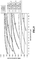
- Fig. 9 illustrates the relation between the effective refractive index and the waveguide width for each of the light beams with the wavelengths ⁇ 1, ⁇ 2, and ⁇ 3 in the 0-th, first, and second order modes in the optical multiplexing circuit according to this example 2.
- the waveguide thickness is 3.6 ⁇ m, and the relative refractive index difference ⁇ is 0.45%.
- the waveguide widths of the first to third optical waveguides 201 to 203 are, for example, 1.5 ⁇ m (the left end of Fig. 9 )
- the waveguide width with which the effective refractive index of the light beam with the wavelength ⁇ 1' in the second order mode is equal to the effective refractive index of the light beam with the wavelength ⁇ 1' in the 0-th order mode is 6.75 ⁇ m.
- the waveguide width of the first portion 204 1 of the multiplexing optical waveguide 204 which is arranged close to the first multiplexing part 205, is set to 6.75 ⁇ m so that the light beam with the wavelength ⁇ 1' in the 0-th order mode propagating through the first optical waveguide 201 can transfer to the first portion 204 1 of the multiplexing optical waveguide 204.
- the light beam with the wavelength ⁇ 1' in the 0-th order mode propagating through the first optical waveguide 201 undergoes waveguide mode conversion into the second order mode and is coupled to the multiplexing optical waveguide 204 at the first multiplexing part 205.
- the coupled light beam with the wavelength ⁇ 1' in the second order mode is multiplexed with the light beams with the wavelengths ⁇ 1, ⁇ 2, and ⁇ 3 in the 0-th order mode propagating through the multiplexing optical waveguide 204.
- the coupling length is 3280 ⁇ m. Also, as illustrated in Fig.
- the light beams with the wavelengths ⁇ 1, ⁇ 2, and ⁇ 3 in the 0-th order mode propagating through the multiplexing optical waveguide 204 are hardly coupled to the first optical waveguide 201 since their effective refractive indexes are greatly different.
- the light beam with the wavelength ⁇ 2' in the 0-th order mode propagating through the second optical waveguide 202 undergoes waveguide mode conversion into the second order mode and is coupled to the multiplexing optical waveguide 204 at the second multiplexing part 206.
- the waveguide width of the second portion 204 2 of the multiplexing optical waveguide 204 which is arranged close to the second multiplexing part 206, may be 7.15 ⁇ m so that the effective refractive index of the light beam with the wavelength ⁇ 2' in the second order mode can be equal to the effective refractive index of the light beam with the wavelength ⁇ 2' in the 0-th order mode.
- the coupling length is 2380 ⁇ m. Also, as illustrated in Fig. 9 , the light beams with the wavelengths ⁇ 1, ⁇ 2, and ⁇ 3 in the 0-th order mode and the light beam with the wavelength ⁇ 1' in the second order mode propagating through the multiplexing optical waveguide 204 are hardly coupled to the second optical waveguide 202 since their effective refractive indexes are greatly different.
- the light beam with the wavelength ⁇ 3' in the 0-th order mode propagating through the third optical waveguide 203 undergoes waveguide mode conversion into the second order mode and is coupled to the multiplexing optical waveguide 204 at the third multiplexing part 207.
- the waveguide width of the third portion 204 3 of the multiplexing optical waveguide 204, which is arranged close to the third multiplexing part 207 may be 8.00 ⁇ m so that the effective refractive index of the light beam with the wavelength ⁇ 3' in the second order mode can be equal to the effective refractive index of the light beam with the wavelength ⁇ 3' in the 0-th order mode.
- the coupling length is 900 ⁇ m. Also, as illustrated in Fig. 9 , the light beams with the wavelengths ⁇ 1, ⁇ 2, and ⁇ 3 in the 0-th order mode and the light beams with the wavelengths ⁇ 1' and ⁇ 2' in the second order mode propagating through the multiplexing optical waveguide 204 are hardly coupled to the third optical waveguide 203 since their effective refractive indexes are greatly different.
- the light beams with the wavelengths ⁇ 1', ⁇ 2', and ⁇ 3' are converted into second order mode light beams and coupled to the multiplexing optical waveguide 204 to thereby be multiplexed with the light beams with the wavelengths ⁇ 1, ⁇ 2, and ⁇ 3 propagating through the multiplexing optical waveguide 204.
- the multiplexed light beam can be output from the output waveguide 208.
- a multiplexed light beam with a desired spot diameter can be output as the multiplexed light beam by changing the waveguide width of the third portion 204 3 of the multiplexing optical waveguide 204 to a desired waveguide width.
- a multiplexed light beam with a small spot diameter can be output by changing the waveguide width to a small waveguide width.
- the waveguide width should be changed so as to avoid cutoff of the higher order mode light beam.
- the waveguide width of the output waveguide 208 needs to be not smaller than 5.8 ⁇ m, which is the minimum waveguide width allowing propagation of the light beam with the wavelength ⁇ 3' in the second order mode.
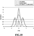
- Fig. 10 illustrates the beam profiles of a 0-th order mode light beam, a second order mode light beam, and a multiplexed light beam of the 0-th order mode light beam and the second order mode light beam.
- an amplitude E(p)(x) of the light beam in each mode can be approximately expressed by the functions below.
- the multiplexed beam profile can be rendered into a profile close to a Gaussian profile by adjusting the intensity of the light beam in each mode.
- the multiplexed light beam of the 0-th order mode light beam and the second order mode light beam has higher intensity and a smaller spot diameter than the 0-th order mode light beam and the second order mode light beam.
- a multiplexed light beam with higher intensity and a smaller spot diameter can be output by multiplexing, in a waveguide in which light beams with R, G, and B wavelengths in the 0-th order mode are multiplexed, light beams with the R, G, and B wavelengths in a different waveguide mode and emitting them.
- the light beams with the wavelength ⁇ 1, ⁇ 2, and ⁇ 3 can be light beams with wavelengths in blue (400 to 495 nm), green (495 to 570 nm), and red (620 to 750 nm) wavelength bands, respectively.
- An optical multiplexing circuit according to an embodiment of the present invention will be specifically described with reference to Fig. 11 .
- an optical multiplexing circuit will be discussed which has a function of coupling and multiplexing only light beams with desired wavelengths as in example 1 and a function of multiplexing light beams with wavelengths in different waveguide modes to thereby output a multiplexed light beam with higher intensity as in example 2.
- Fig. 11 illustrates an optical multiplexing circuit including first to fifth optical waveguides 301 to 305 into which light beams with wavelengths ⁇ 1 to ⁇ 5 are input, respectively, first and second MM conversion waveguides 306 and 307, first to fourth coupling parts 308 to 311, first and second multiplexing parts 312 and 313, and an output waveguide 314 coupled to the first optical waveguide 301.
- the first to fifth optical waveguides 301 to 305 and the first and second MM conversion waveguides 306 and 307 are formed of a lower cladding layer provided on a substrate, a core layer higher in refractive index than the lower cladding layer, and an upper cladding layer provided on the core layer.
- the upper cladding layer is provided so as to surround the core layer.
- the first optical waveguide 301 can be a multi-mode waveguide.
- the second to fifth optical waveguides 302 to 305 can be single-mode waveguides. As illustrated in Fig. 11 , the first to fifth optical waveguides 301 to 305 and the first and second MM conversion waveguides 306 and 307 are arranged side by side along the light travel direction.
- the first optical waveguide 301 includes first and second portions 301 1 and 301 2 differing from each other in waveguide width.
- the first and second portions 301 1 and 301 2 and the output waveguide 315 are each coupled to another by a tapered waveguide.
- the first to fifth optical waveguides 301 to 305 and the first and second MM conversion waveguides 306 and 307 differ from each other in waveguide width.
- the first to fourth coupling parts 308 to 311 are directional couplers formed by arranging the second optical waveguide 302 and the first MM conversion waveguide 306 close to each other, arranging the first optical waveguide 301 and the first MM conversion waveguide 306 close to each other, arranging the third optical waveguide 303 and the second MM conversion waveguide 307 to each other, and arranging the first optical waveguide 301 and the second MM conversion waveguide 307 to each other, respectively.
- the first and second multiplexing parts 312 and 313 are directional couplers formed by arranging the fourth optical waveguide 304 and the first optical waveguide 301 close to each other and arranging the fifth optical waveguide 305 and the first optical waveguide 301 close to each other, respectively.
- the waveguide widths of the first and second optical waveguides 301 and 302 and the waveguide width of the first MM conversion waveguide 306 are set such that the effective refractive index of the second optical waveguide 302 with the light beam with the wavelength ⁇ 2 in the 0-th order mode is equal to the effective refractive index of the first MM conversion waveguide 306 with the light beam with the wavelength ⁇ 2 in a higher order mode and that the effective refractive index of the first optical waveguide 301 with the light beam with the wavelength ⁇ 1 in the 0-th order mode is not equal to the effective refractive index of the first MM conversion waveguide 306 with each light beam with the wavelength ⁇ in the higher order mode.
- the waveguide widths of the first and third optical waveguides 301 and 303 and the waveguide width of the second MM conversion waveguide 307 are set such that the effective refractive index of the third optical waveguide 303 with the light beam with the wavelength ⁇ 3 in the 0-th order mode is equal to the effective refractive index of the second MM conversion waveguide 307 with the light beam with the wavelength ⁇ 3 in the higher order mode and that the effective refractive index of the first optical waveguide 301 with the light beam with the wavelength ⁇ 1 in the 0-th order mode is not equal to the effective refractive index of the second MM conversion waveguide 307 with each of the light beams with the wavelengths ⁇ .
- the waveguide width of the first portion 204 1 is set such that the effective refractive index of the fourth optical waveguide 304 with the light beam with the wavelength ⁇ 2' in the 0-th order mode is equal to the effective refractive index of the first portion 301 1 of the first optical waveguide 301 with the light beam with the wavelength ⁇ 2' in a higher order mode and that the effective refractive indexes of the first portion 301 1 of the first optical waveguide 301 with the light beams with the wavelengths ⁇ 1, ⁇ 2, and ⁇ 3 in the higher order mode are not equal to the effective refractive indexes of the fourth optical waveguide 304 with the light beams with the wavelengths ⁇ 1, ⁇ 2, and ⁇ 3 in the 0-th order mode.
- the waveguide width of the second portion 204 2 is set such that the effective refractive index of the fifth optical waveguide 305 with the light beam with the wavelength ⁇ 3' in the 0-th order mode is equal to the effective refractive index of the second portion 301 2 of the first optical waveguide 301 with the light beam with the wavelength ⁇ 3' in the higher order mode and that the effective refractive indexes of the second portion 301 2 of the first optical waveguide 301 with the light beams with the wavelengths ⁇ 1, ⁇ 2, and ⁇ 3 in the higher order mode are not equal to the effective refractive indexes of the fifth optical waveguide 305 with the light beams with the wavelengths ⁇ 1, ⁇ 2, and ⁇ 3 in the 0-th order mode.
- the linewidth is dependent on the light source of the incoming light beam but is assumed to be about 1 nm or smaller.
- the operation of the optical multiplexing circuit according to the embodiment of the present invention will be described below.
- the light beam with the wavelength ⁇ 2 having input to the second optical waveguide 302 undergoes waveguide mode conversion into the first order mode and transfers to the first MM conversion waveguide 306 at the first coupling part 308, and further undergoes waveguide mode conversion into the 0-th order mode and transfers to the first optical waveguide 301 at the second coupling part 309.
- the light beam with the wavelength ⁇ 3 having input to the third optical waveguide 303 undergoes waveguide mode conversion into the first order mode and transfers to the second MM conversion waveguide 307 at the third coupling part 310, and further undergoes waveguide mode conversion into the 0-th order mode and transfers to the first optical waveguide 301 at the fourth coupling part 311.
- the second and fourth coupling parts 309 and 311 are designed so as not to satisfy conditions for coupling to the first and second MM conversion waveguides 306 and 307.
- the light beam with the wavelength ⁇ 1 in the 0-th order mode having input to the first optical waveguide 301 does not transfer to either of the first and second MM conversion waveguides 306 and 307 at the respective second and fourth coupling parts 309 and 311 but is transmitted by the second and fourth coupling parts 309 and 311.
- the optical multiplexing circuit according to the embodiment can implement the function of coupling and multiplexing only light beams with desired wavelengths as in example 1.
- the light beam with the wavelength ⁇ 2' in the 0-th order mode propagating through the fourth optical waveguide 304 undergoes waveguide mode conversion into the second order mode and is coupled to the first portion 301 1 of the first optical waveguide 301 at the first multiplexing part 312.
- the coupled light beam with the wavelength ⁇ 2' in the second order mode is multiplexed with the light beams with the wavelengths ⁇ 1, ⁇ 2, and ⁇ 3 in the 0-th order mode propagating through the first portion 301 1 of the first optical waveguide 301 and input into the second portion 301 2 of the first optical waveguide 301.
- the light beam with the wavelength ⁇ 3' in the 0-th order mode propagating through the fifth optical waveguide 305 undergoes waveguide mode conversion into the second order mode and is coupled to the second portion 301 2 of the first waveguide 301 at the second multiplexing part 313.
- the coupled light beam with the wavelength ⁇ 3' in the second order mode is multiplexed with the multiplexed light beam propagating through the second portion 301 2 of the first waveguide 301 and output from the output waveguide 314.
- the optical multiplexing circuit according to the embodiment can implement the function of multiplexing light beams with wavelengths in different waveguide modes to thereby output a multiplexed light beam with higher intensity as in example 2.
- the waveguide thickness is 3.6 ⁇ m
- the relative refractive index difference ⁇ 0.45%
- the inter-waveguide gaps at the first to fourth coupling parts 308 to 311 and between the fourth optical waveguide 304 and the first portion 301 1 and between the fifth optical waveguide 305 and the second portion 301 2 are 2.5 ⁇ m
- the coupling lengths at the first to fourth coupling parts 308 to 311 are 702 ⁇ m
- the coupling length at the first multiplexing part 312 is 2380 ⁇ m
- the coupling length at the second multiplexing part 313 900 ⁇ m
- the waveguide widths of the first to fifth optical waveguides 301 to 305 are 1.5 ⁇ m, as in examples 1 and 2.
- the optical multiplexing circuit it is possible to make the optical multiplexing circuit according to the embodiment by setting the waveguide width of the first MM conversion waveguide 306 to 4.3 ⁇ m, the waveguide width of the second MM conversion waveguide 307 to 4.8 ⁇ m, the waveguide width of the first portion 301 1 to 7.15 ⁇ m, and the waveguide width of the second portion 301 2 to 8.00 ⁇ m based on Figs. 5 and 9 .
- optical multiplexing circuits for R, G, and B which are three primary colors of visible light, have been exemplarily discussed. It is, however, obvious that the present invention is applicable as an optical multiplexing/demultiplexing circuit that multiplexes or demultiplexes a plurality of light beams with different wavelengths.
Landscapes
- Physics & Mathematics (AREA)
- General Physics & Mathematics (AREA)
- Optics & Photonics (AREA)
- Engineering & Computer Science (AREA)
- Microelectronics & Electronic Packaging (AREA)
- Optical Integrated Circuits (AREA)
Claims (3)
- Optische Multiplexschaltung, die aufweist:(a) einen ersten optischen Wellenleiter (301) zum Eingeben eines ersten Lichtstrahls mit einer ersten Wellenlänge in einer Mode nullter Ordnung;(b1) einen zweiten optischen Wellenleiter (302) zum Eingeben eines zweiten Lichtstrahls in der Mode nullter Ordnung,(b2) einen dritten optischen Wellenleiter (303) zum Eingeben eines dritten Lichtstrahls in der Mode nullter Ordnung, wobei die Wellenlängen des zweiten Lichtstrahls und des dritten Lichtstrahls verschieden von der ersten Wellenlänge und untereinander verschieden sind;(c1) einen ersten Multimodenumwandlungswellenleiter (306), der zwischen dem ersten optischen Wellenleiter und dem zweiten optischen Wellenleiter bereitgestellt ist;(c2) einen zweiten Multimodenumwandlungswellenleiter (307), der zwischen dem ersten optischen Wellenleiter und dem dritten optischen Wellenleiter bereitgestellt ist;(d1) ein erstes Kopplungsteil (308), das zwischen dem zweiten optischen Wellenleiter (302) und dem ersten Multimodenumwandlungswellenleiter (306) mit einer ersten Zwischenwellenleiterlücke zum Umwandeln einer Wellenleitermode des zweiten Lichtstrahls, der durch den zweiten optischen Wellenleiter propagiert, in eine Mode höherer Ordnung bereitgestellt ist, um den zweiten Lichtstrahl, der in die Mode höherer Ordnung umgewandelt ist, in den ersten Multimodenumwandlungswellenleiter (306) zu koppeln;(d2) ein drittes Kopplungsteil (310), das zwischen dem dritten optischen Wellenleiter (303) und dem zweiten Multimodenumwandlungswellenleiter (307) mit einer dritten Zwischenwellenleiterlücke zum Umwandeln einer Wellenleitermode des dritten Lichtstrahls, der durch den dritten optischen Wellenleiter propagiert, in eine Mode höherer Ordnung bereitgestellt ist, um den dritten Lichtstrahl, der in die Mode höherer Ordnung umgewandelt ist, in den zweiten Multimodenumwandlungswellenleiter (307) zu koppeln;(e1) ein zweites Kopplungsteil (309), das zwischen dem ersten Multimodenumwandlungswellenleiter (306) und dem ersten optischen Wellenleiter (301) mit einer zweiten Zwischenwellenleiterlücke zum Umwandeln einer Wellenleitermode des zweiten Lichtstrahls, der durch den ersten Multimodenumwandlungswellenleiter (306) propagiert, in die Mode nullter Ordnung bereitgestellt ist, um den zweiten Lichtstrahl, der in die Mode nullter Ordnung umgewandelt ist, in den ersten optischen Wellenleiter (301) zu koppeln, wobei der erste Lichtstrahl durch den ersten optischen Wellenleiter (301) propagiert;(e2) ein viertes Kopplungsteil (311), das zwischen dem zweiten Multimodenumwandlungswellenleiter (307) und dem ersten optischen Wellenleiter (301) mit einer vierten Zwischenwellenleiterlücke zum Umwandeln einer Wellenleitermode des dritten Lichtstrahls, der durch den zweiten Multimodenumwandlungswellenleiter (307) propagiert, in die Mode nullter Ordnung umzuwandeln, bereitgestellt ist, um den dritten Lichtstrahl, der in die Mode nullter Ordnung umgewandelt ist, in den ersten optischen Wellenleiter (301) zu koppeln, wobei der erste Lichtstrahl durch den ersten optischen Wellenleiter (301) propagiert;(f1) einen vierten optischen Wellenleiter (304) zum Eingeben eines jeweiligen vierten Lichtstrahls in der Mode nullter Ordnung, wobei eine Wellenlänge des vierten Lichtstrahls größer als die Wellenlänge des zweiten Lichtstrahls um weniger als eine Linienbreite des zweiten Lichtstrahls ist;(f2) einen fünften optischen Wellenleiter (305) zum Eingeben eines fünften Lichtstrahls in der Mode nullter Ordnung, wobei eine Wellenlänge des fünften Lichtstrahls größer als die Wellenlänge des dritten Lichtstrahls um weniger als eine Linienbreite des dritten Lichtstrahls ist;(g1) ein erstes Multiplexteil (312), das zwischen dem vierten optischen Wellenleiter (304) und einem ersten Anteil (3011) des ersten optischen Wellenleiters (301) nahe dem vierten optischen Wellenleiter (304) zum Umwandeln einer Wellenleitermode des vierten Lichtstrahls, der durch den vierten optischen Wellenleiter propagiert, und eine Mode höherer Ordnung bereitgestellt ist, um den vierten Lichtstrahl, der in die Mode höherer Ordnung umgewandelt ist, in den ersten Anteil (3011) des ersten optischen Wellenleiters (301) zu koppeln,(g2) ein zweites Multiplexteil (313), das zwischen dem fünften optischen Wellenleiter (305) und einem zweiten Anteil (3012) des ersten optischen Wellenleiters (301) nahe dem fünften optischen Wellenleiter (305) zum Umwandeln einer Wellenleitermode des fünften Lichtstrahls, der durch den fünften optischen Wellenleiter propagiert, in eine Mode höherer Ordnung bereitgestellt ist, um den fünften Lichtstrahl, der in die Mode höherer Ordnung umgewandelt ist, in den zweiten Anteil (3012) des ersten optischen Wellenleiters (301) zu koppeln, wobeiin dem ersten optischen Wellenleiter der zweite Lichtstrahl, der in die Mode nullter Ordnung umgewandelt ist und durch das zweite Kopplungsteil gekoppelt ist, der dritte Lichtstrahl, der in die Mode nullter Ordnung umgewandelt ist und durch das vierte Kopplungsteil gekoppelt ist, und der erste Lichtstrahl, der durch das zweite Kopplungsteil und das vierte Kopplungsteil transmittiert ist, multiplext werden und in den ersten Anteil (3011) des ersten optischen Wellenleiters (301) eingegeben werden,der erste optische Wellenleiter (301) und der erste Anteil (3011) mit einem ersten abgeschrägten Wellenleiter gekoppelt sind,der erste Anteil (3011) und der zweite Anteil (3012) mit einem zweiten abgeschrägten Wellenleiter gekoppelt sind,Wellenleiterbreiten der ersten und zweiten Anteile (3011, 3012) voneinander verschieden sind;Wellenlängen der ersten bis fünften Lichter untereinander verschieden sind; und(h) einen Ausgabewellenleiter (314), der mit dem zweiten Anteil (3012) zum Ausgeben eines multiplexten Lichtstrahls, der aus den ersten, zweiten, dritten, vierten und fünften Lichtstrahlen multiplext ist;(i1) wobei die Wellenleiterbreite des ersten optischen Wellenleiters (301) und Wellenleiterbreiten des zweiten optischen Wellenleiters (302) und des ersten Multimodenumwandlungswellenleiters (306) so eingestellt sind, dass ein effektiver Brechungsindex des zweiten optischen Wellenleiters (302) für den zweiten Lichtstrahl in der Mode nullter Ordnung gleich einem effektiven Brechungsindex des ersten Multimodenumwandlungswellenleiters (306) für den zweiten Lichtstrahl, der in die Mode höherer Ordnung umgewandelt ist, ist, und dass ein effektiver Brechungsindex des ersten Multimodenumwandlungswellenleiters (306) für den ersten Lichtstrahl in der Mode höherer Ordnung nicht gleich einem effektiven Brechungsindex des ersten optischen Wellenleiters (301) für den ersten Lichtstrahl in der Mode nullter Ordnung ist,(i2) wobei die Wellenleiterbreite des ersten optischen Wellenleiters (301) und Wellenleiterbreiten des dritten optischen Wellenleiters (303) und des zweiten Multimodenumwandlungswellenleiters (307) so eingestellt sind, dass ein effektiver Brechungsindex des dritten optischen Wellenleiters (303) für den jeweiligen dritten Lichtstrahl in der Mode nullter Ordnung gleich einem effektiven Brechungsindex des zweiten Multimodenumwandlungswellenleiters (307) für den dritten Lichtstrahl, der in die Mode höherer Ordnung umgewandelt ist, ist, und dass ein effektiver Brechungsindex des zweiten Multimodenumwandlungswellenleiters (307) für den ersten Lichtstrahl in der Mode höherer Ordnung nicht gleich einem effektiven Brechungsindex des ersten optischen Wellenleiters (301) für den ersten Lichtstrahl in der Mode nullter Ordnung ist,(j1) Wellenleiterbreiten des ersten Anteils (3011) des ersten optischen Wellenleiters (301) und des vierten optischen Wellenleiters (304) so eingestellt sind, dass ein effektiver Brechungsindex des vierten optischen Wellenleiters (304) für den vierten Lichtstrahl in der Mode nullter Ordnung gleich einem effektiven Brechungsindex des ersten Anteils (3011) des ersten optischen Wellenleiters (301) für den vierten Lichtstrahl in der Mode höherer Ordnung ist, und dass effektive Brechungsindizes des ersten Anteils (3011) für die ersten bis dritten Lichtstrahlen in der Mode höherer Ordnung nicht gleich den effektiven Brechungsindizes des vierten optischen Wellenleiters (304) für die ersten bis dritten Lichtstrahlen in der Mode nullter Ordnung sind;(j2) Wellenleiterbreiten des zweiten Anteils (3012) des ersten optischen Wellenleiters (301) und des fünften optischen Wellenleiters (305) so eingestellt sind, dass ein effektiver Brechungsindex des fünften optischen Wellenleiters (305) für den fünften Lichtstrahl in der Mode nullter Ordnung gleich einem effektiven Brechungsindex des zweiten Anteils (3012) des ersten optischen Wellenleiters (301) für den fünften Lichtstrahl in der Mode höherer Ordnung ist, und dass effektive Brechungsindizes des zweiten Anteils (3012) für die ersten bis dritten Lichtstrahlen in der Mode höherer Ordnung nicht gleich effektiven Brechungsindizes des fünften optischen Wellenleiters (305) für die ersten bis dritten Lichtstrahlen in der Mode nullter Ordnung sind.
- Optische Multiplexschaltung nach Anspruch 1, wobei der erste optische Wellenleiter ein Multimodenwellenleiter ist und die zweiten und dritten Wellenleiter Einzelmodenwellenleiter sind.
- Optische Multiplexschaltung nach Anspruch 1, wobei der multiplexte Lichtstrahl zumindest eine Wellenlänge von jedem der Wellenlängenbänder von 400 bis 495 nm, 495 bis 570 nm und 620 bis 750 nm aufweist.
Applications Claiming Priority (4)
| Application Number | Priority Date | Filing Date | Title |
|---|---|---|---|
| JP2016029366 | 2016-02-18 | ||
| JP2016029361 | 2016-02-18 | ||
| PCT/JP2017/005975 WO2017142076A1 (ja) | 2016-02-18 | 2017-02-17 | 光合波回路 |
| EP17753330.4A EP3418783A4 (de) | 2016-02-18 | 2017-02-17 | Optische multiplexer-schaltung |
Related Parent Applications (1)
| Application Number | Title | Priority Date | Filing Date |
|---|---|---|---|
| EP17753330.4A Division EP3418783A4 (de) | 2016-02-18 | 2017-02-17 | Optische multiplexer-schaltung |
Publications (2)
| Publication Number | Publication Date |
|---|---|
| EP3767352A1 EP3767352A1 (de) | 2021-01-20 |
| EP3767352B1 true EP3767352B1 (de) | 2022-04-20 |
Family
ID=59625276
Family Applications (4)
| Application Number | Title | Priority Date | Filing Date |
|---|---|---|---|
| EP20175143.5A Active EP3767352B1 (de) | 2016-02-18 | 2017-02-17 | Optische multiplexer-schaltung |
| EP20209717.6A Withdrawn EP3800491A1 (de) | 2016-02-18 | 2017-02-17 | Optische multiplexer-schaltung |
| EP17753330.4A Ceased EP3418783A4 (de) | 2016-02-18 | 2017-02-17 | Optische multiplexer-schaltung |
| EP21177930.1A Active EP3896505B1 (de) | 2016-02-18 | 2017-02-17 | Optische multiplexer-schaltung |
Family Applications After (3)
| Application Number | Title | Priority Date | Filing Date |
|---|---|---|---|
| EP20209717.6A Withdrawn EP3800491A1 (de) | 2016-02-18 | 2017-02-17 | Optische multiplexer-schaltung |
| EP17753330.4A Ceased EP3418783A4 (de) | 2016-02-18 | 2017-02-17 | Optische multiplexer-schaltung |
| EP21177930.1A Active EP3896505B1 (de) | 2016-02-18 | 2017-02-17 | Optische multiplexer-schaltung |
Country Status (5)
| Country | Link |
|---|---|
| US (2) | US10649144B2 (de) |
| EP (4) | EP3767352B1 (de) |
| JP (1) | JP6572377B2 (de) |
| CN (2) | CN111487713B (de) |
| WO (1) | WO2017142076A1 (de) |
Families Citing this family (18)
| Publication number | Priority date | Publication date | Assignee | Title |
|---|---|---|---|---|
| EP3767352B1 (de) | 2016-02-18 | 2022-04-20 | Nippon Telegraph and Telephone Corporation | Optische multiplexer-schaltung |
| CN108254829A (zh) * | 2018-01-04 | 2018-07-06 | 华南师范大学 | 一种双重非对称的纵向模式转换器的设计方法 |
| JP6994220B2 (ja) * | 2018-03-01 | 2022-01-14 | 日本電信電話株式会社 | 波長合波器 |
| JP7172271B2 (ja) * | 2018-08-10 | 2022-11-16 | 日本電信電話株式会社 | 光合波器およびrgbカプラ |
| JP7189432B2 (ja) * | 2019-01-10 | 2022-12-14 | 日本電信電話株式会社 | 光信号処理装置 |
| JP7172642B2 (ja) * | 2019-01-23 | 2022-11-16 | 日本電信電話株式会社 | モード合分波光回路 |
| JP7120053B2 (ja) * | 2019-01-29 | 2022-08-17 | 日本電信電話株式会社 | 光回路 |
| CN112514184A (zh) * | 2019-03-13 | 2021-03-16 | 国立大学法人福井大学 | 光波导路型光合波器、光波导路型合波光源光学装置以及图像投射装置 |
| WO2020245923A1 (ja) * | 2019-06-04 | 2020-12-10 | 日本電信電話株式会社 | 光回路 |
| JPWO2021002254A1 (de) * | 2019-07-02 | 2021-01-07 | ||
| JP7287242B2 (ja) * | 2019-11-06 | 2023-06-06 | 住友電気工業株式会社 | 光モジュール |
| US11768342B2 (en) * | 2020-05-18 | 2023-09-26 | Nippon Telegraph And Telephone Corporation | Optical multiplexing circuit and optical source |
| US12050342B2 (en) * | 2021-02-05 | 2024-07-30 | University Of Fukui | Optical multiplexer and optical multiplexing method |
| JP2023104721A (ja) * | 2022-01-18 | 2023-07-28 | セーレンKst株式会社 | 光合波器 |
| CN114280729B (zh) * | 2022-02-10 | 2024-06-14 | 苏州龙马璞芯芯片科技有限公司 | 光波导路型合光器及使用该合光器的投影装置 |
| CN114966969B (zh) * | 2022-05-27 | 2024-05-24 | 师大海能应急科技(清远)有限公司 | 一种基于不对称定向耦合器的平行多模交叉结构 |
| US11968034B2 (en) | 2022-08-18 | 2024-04-23 | X Development Llc | Metastructured photonic devices for binary tree multiplexing or demultiplexing of optical signals |
| JP2024058207A (ja) * | 2022-10-14 | 2024-04-25 | Tdk株式会社 | 光合波器及び可視光光源モジュール |
Citations (1)
| Publication number | Priority date | Publication date | Assignee | Title |
|---|---|---|---|---|
| US20130315537A1 (en) * | 2012-05-23 | 2013-11-28 | Mitsubishi Electric Corporation | Optical multiplexing/demultiplexing device |
Family Cites Families (21)
| Publication number | Priority date | Publication date | Assignee | Title |
|---|---|---|---|---|
| JP4652507B2 (ja) * | 1998-12-25 | 2011-03-16 | 古河電気工業株式会社 | 光導波路回路とその製造方法 |
| US6603592B1 (en) * | 2000-09-26 | 2003-08-05 | Lucent Technologies Inc. | Optical wavelength converter |
| US20040028337A1 (en) * | 2000-11-14 | 2004-02-12 | Ilya Vorobeichik | Optical mode coupling devices and an optical switch matrix based thereon |
| JP2004093884A (ja) * | 2002-08-30 | 2004-03-25 | Kyocera Corp | 異波長多重光の合分波装置並びにこれを利用した光増幅器とase光源 |
| US20040096141A1 (en) * | 2002-11-18 | 2004-05-20 | Harmeet Singh | Optical multiplexer |
| US7961997B2 (en) | 2003-09-22 | 2011-06-14 | Celight, Inc. | Space diversity optical receiver and system and method using the same |
| JP4760129B2 (ja) * | 2005-05-20 | 2011-08-31 | 住友ベークライト株式会社 | 光導波路構造体 |
| WO2008108422A1 (ja) * | 2007-03-07 | 2008-09-12 | Nec Corporation | 光導波路モジュール |
| US7539373B1 (en) * | 2007-11-26 | 2009-05-26 | Onechip Photonics Inc. | Integrated lateral mode converter |
| CN101504472A (zh) * | 2008-02-08 | 2009-08-12 | 冲电气工业株式会社 | 光合波/分波元件 |
| WO2010084796A1 (ja) * | 2009-01-23 | 2010-07-29 | 株式会社フジクラ | 光合波器及びファイバレーザ |
| WO2010137661A1 (ja) * | 2009-05-28 | 2010-12-02 | シチズンホールディングス株式会社 | 光源装置 |
| US8965156B2 (en) * | 2010-08-12 | 2015-02-24 | Octrolix Bv | Beam combiner |
| US9306670B2 (en) * | 2011-09-27 | 2016-04-05 | Nippon Telegraph And Telephone Corporation | Optical coupling/splitting device, two-way optical propagation device, and optical-transmit-receive system |
| JP6028339B2 (ja) * | 2012-02-27 | 2016-11-16 | 沖電気工業株式会社 | 波長選択性経路切換素子 |
| JP5988100B2 (ja) * | 2012-12-14 | 2016-09-07 | 日本電信電話株式会社 | モード合分波器 |
| JP6000904B2 (ja) * | 2013-06-27 | 2016-10-05 | 株式会社フジクラ | 偏波変換素子 |
| JP6346454B2 (ja) * | 2014-02-17 | 2018-06-20 | 株式会社フジクラ | 基板型導波路素子、及び、光変調器 |
| US10408999B2 (en) * | 2014-05-09 | 2019-09-10 | National University Corporation University Of Fukui | Multiplexer |
| CN104749707A (zh) * | 2015-01-28 | 2015-07-01 | 浙江大学 | 一种基于弱限制大截面光波导的双偏振模式复用-解复用器 |
| EP3767352B1 (de) * | 2016-02-18 | 2022-04-20 | Nippon Telegraph and Telephone Corporation | Optische multiplexer-schaltung |
-
2017
- 2017-02-17 EP EP20175143.5A patent/EP3767352B1/de active Active
- 2017-02-17 CN CN202010327303.XA patent/CN111487713B/zh active Active
- 2017-02-17 EP EP20209717.6A patent/EP3800491A1/de not_active Withdrawn
- 2017-02-17 WO PCT/JP2017/005975 patent/WO2017142076A1/ja not_active Ceased
- 2017-02-17 CN CN201780011275.7A patent/CN108700706B/zh active Active
- 2017-02-17 JP JP2018500229A patent/JP6572377B2/ja active Active
- 2017-02-17 US US16/077,940 patent/US10649144B2/en active Active
- 2017-02-17 EP EP17753330.4A patent/EP3418783A4/de not_active Ceased
- 2017-02-17 EP EP21177930.1A patent/EP3896505B1/de active Active
-
2020
- 2020-04-10 US US16/845,523 patent/US11112563B2/en active Active
Patent Citations (1)
| Publication number | Priority date | Publication date | Assignee | Title |
|---|---|---|---|---|
| US20130315537A1 (en) * | 2012-05-23 | 2013-11-28 | Mitsubishi Electric Corporation | Optical multiplexing/demultiplexing device |
Also Published As
| Publication number | Publication date |
|---|---|
| EP3418783A1 (de) | 2018-12-26 |
| EP3418783A4 (de) | 2019-11-20 |
| US20190056552A1 (en) | 2019-02-21 |
| EP3896505A1 (de) | 2021-10-20 |
| CN108700706A (zh) | 2018-10-23 |
| US11112563B2 (en) | 2021-09-07 |
| EP3896505B1 (de) | 2023-10-11 |
| CN111487713A (zh) | 2020-08-04 |
| WO2017142076A1 (ja) | 2017-08-24 |
| US20200241206A1 (en) | 2020-07-30 |
| EP3800491A1 (de) | 2021-04-07 |
| CN111487713B (zh) | 2023-01-24 |
| US10649144B2 (en) | 2020-05-12 |
| CN108700706B (zh) | 2020-08-04 |
| JPWO2017142076A1 (ja) | 2018-08-09 |
| JP6572377B2 (ja) | 2019-09-11 |
| EP3767352A1 (de) | 2021-01-20 |
Similar Documents
| Publication | Publication Date | Title |
|---|---|---|
| EP3767352B1 (de) | Optische multiplexer-schaltung | |
| US8532446B2 (en) | Scalable silicon photonic multiplexers and demultiplexers | |
| US8811786B2 (en) | Coupled system multi-core fiber, coupling mode multiplexer and demultiplexer, system for transmission using multi-core fiber and method for transmission using multi-core fiber | |
| EP1226461B1 (de) | Phasar mit flacher durchlasskurve | |
| WO2014030575A1 (ja) | 光導波路素子 | |
| JP6691518B2 (ja) | 光集積回路 | |
| Shi et al. | Silicon CWDM demultiplexers using contra-directional couplers | |
| EP3203282B1 (de) | Rippenartiger optischer wellenleiter und optischer multiplexer/demultiplexer mit verwendung davon | |
| EP3078997B1 (de) | Photonische integrierte vorrichtung | |
| JP2013068909A (ja) | 光素子 | |
| JP4477260B2 (ja) | 導波路型光カプラおよび該導波路型光カプラを用いた光合分波器 | |
| WO2014030576A1 (ja) | 光導波路素子 | |
| US20100247036A1 (en) | Flat-top response arrayed waveguide grating | |
| US6728447B2 (en) | Optical multiplexer/demultiplexer | |
| JP4554209B2 (ja) | 光フィルタ | |
| US11921320B2 (en) | Optical circuit | |
| JP7079391B2 (ja) | 光伝送装置及び光素子 | |
| Gupta et al. | Integrated silicon photonics directional couplers for WDM applications | |
| JP3931834B2 (ja) | 光波長合分波器 | |
| US12451966B1 (en) | Optical communication systems and silicon photonics passive multiplexers and demultiplexers having Mach-Zehnder interferometer structures | |
| US20260050123A1 (en) | Mach-zehnder interferometers with phase delay arms having a metamaterial region | |
| US20250323727A1 (en) | Optical Signal Processing Device and Optical Signal Transmission System | |
| Suzuki et al. | 40-wavelength channelized tunable optical dispersion compensator with increased bandwidth consisting of arrayed waveguide gratings and liquid crystal on silicon | |
| Magden et al. | Mode-evolution-based, broadband 1× 2 port high-pass/low-pass filter for silicon photonics | |
| WO2017069240A1 (ja) | 光分波器、光合波器および光通信システム |
Legal Events
| Date | Code | Title | Description |
|---|---|---|---|
| PUAI | Public reference made under article 153(3) epc to a published international application that has entered the european phase |
Free format text: ORIGINAL CODE: 0009012 |
|
| STAA | Information on the status of an ep patent application or granted ep patent |
Free format text: STATUS: THE APPLICATION HAS BEEN PUBLISHED |
|
| AC | Divisional application: reference to earlier application |
Ref document number: 3418783 Country of ref document: EP Kind code of ref document: P |
|
| AK | Designated contracting states |
Kind code of ref document: A1 Designated state(s): AL AT BE BG CH CY CZ DE DK EE ES FI FR GB GR HR HU IE IS IT LI LT LU LV MC MK MT NL NO PL PT RO RS SE SI SK SM TR |
|
| STAA | Information on the status of an ep patent application or granted ep patent |
Free format text: STATUS: REQUEST FOR EXAMINATION WAS MADE |
|
| 17P | Request for examination filed |
Effective date: 20210512 |
|
| RBV | Designated contracting states (corrected) |
Designated state(s): AL AT BE BG CH CY CZ DE DK EE ES FI FR GB GR HR HU IE IS IT LI LT LU LV MC MK MT NL NO PL PT RO RS SE SI SK SM TR |
|
| STAA | Information on the status of an ep patent application or granted ep patent |
Free format text: STATUS: EXAMINATION IS IN PROGRESS |
|
| 17Q | First examination report despatched |
Effective date: 20210625 |
|
| GRAP | Despatch of communication of intention to grant a patent |
Free format text: ORIGINAL CODE: EPIDOSNIGR1 |
|
| STAA | Information on the status of an ep patent application or granted ep patent |
Free format text: STATUS: GRANT OF PATENT IS INTENDED |
|
| RIC1 | Information provided on ipc code assigned before grant |
Ipc: G02B 6/293 20060101ALN20211109BHEP Ipc: G02B 6/14 20060101ALN20211109BHEP Ipc: G02B 6/12 20060101AFI20211109BHEP |
|
| INTG | Intention to grant announced |
Effective date: 20211123 |
|
| RIC1 | Information provided on ipc code assigned before grant |
Ipc: G02B 6/293 20060101ALN20211112BHEP Ipc: G02B 6/14 20060101ALN20211112BHEP Ipc: G02B 6/12 20060101AFI20211112BHEP |
|
| GRAS | Grant fee paid |
Free format text: ORIGINAL CODE: EPIDOSNIGR3 |
|
| GRAA | (expected) grant |
Free format text: ORIGINAL CODE: 0009210 |
|
| STAA | Information on the status of an ep patent application or granted ep patent |
Free format text: STATUS: THE PATENT HAS BEEN GRANTED |
|
| AC | Divisional application: reference to earlier application |
Ref document number: 3418783 Country of ref document: EP Kind code of ref document: P |
|
| AK | Designated contracting states |
Kind code of ref document: B1 Designated state(s): AL AT BE BG CH CY CZ DE DK EE ES FI FR GB GR HR HU IE IS IT LI LT LU LV MC MK MT NL NO PL PT RO RS SE SI SK SM TR |
|
| REG | Reference to a national code |
Ref country code: GB Ref legal event code: FG4D |
|
| REG | Reference to a national code |
Ref country code: CH Ref legal event code: EP |
|
| REG | Reference to a national code |
Ref country code: IE Ref legal event code: FG4D |
|
| REG | Reference to a national code |
Ref country code: DE Ref legal event code: R096 Ref document number: 602017056424 Country of ref document: DE |
|
| REG | Reference to a national code |
Ref country code: AT Ref legal event code: REF Ref document number: 1485604 Country of ref document: AT Kind code of ref document: T Effective date: 20220515 |
|
| REG | Reference to a national code |
Ref country code: LT Ref legal event code: MG9D |
|
| REG | Reference to a national code |
Ref country code: NL Ref legal event code: MP Effective date: 20220420 |
|
| REG | Reference to a national code |
Ref country code: AT Ref legal event code: MK05 Ref document number: 1485604 Country of ref document: AT Kind code of ref document: T Effective date: 20220420 |
|
| PG25 | Lapsed in a contracting state [announced via postgrant information from national office to epo] |
Ref country code: NL Free format text: LAPSE BECAUSE OF FAILURE TO SUBMIT A TRANSLATION OF THE DESCRIPTION OR TO PAY THE FEE WITHIN THE PRESCRIBED TIME-LIMIT Effective date: 20220420 |
|
| PG25 | Lapsed in a contracting state [announced via postgrant information from national office to epo] |
Ref country code: SE Free format text: LAPSE BECAUSE OF FAILURE TO SUBMIT A TRANSLATION OF THE DESCRIPTION OR TO PAY THE FEE WITHIN THE PRESCRIBED TIME-LIMIT Effective date: 20220420 Ref country code: PT Free format text: LAPSE BECAUSE OF FAILURE TO SUBMIT A TRANSLATION OF THE DESCRIPTION OR TO PAY THE FEE WITHIN THE PRESCRIBED TIME-LIMIT Effective date: 20220822 Ref country code: NO Free format text: LAPSE BECAUSE OF FAILURE TO SUBMIT A TRANSLATION OF THE DESCRIPTION OR TO PAY THE FEE WITHIN THE PRESCRIBED TIME-LIMIT Effective date: 20220720 Ref country code: LT Free format text: LAPSE BECAUSE OF FAILURE TO SUBMIT A TRANSLATION OF THE DESCRIPTION OR TO PAY THE FEE WITHIN THE PRESCRIBED TIME-LIMIT Effective date: 20220420 Ref country code: HR Free format text: LAPSE BECAUSE OF FAILURE TO SUBMIT A TRANSLATION OF THE DESCRIPTION OR TO PAY THE FEE WITHIN THE PRESCRIBED TIME-LIMIT Effective date: 20220420 Ref country code: GR Free format text: LAPSE BECAUSE OF FAILURE TO SUBMIT A TRANSLATION OF THE DESCRIPTION OR TO PAY THE FEE WITHIN THE PRESCRIBED TIME-LIMIT Effective date: 20220721 Ref country code: FI Free format text: LAPSE BECAUSE OF FAILURE TO SUBMIT A TRANSLATION OF THE DESCRIPTION OR TO PAY THE FEE WITHIN THE PRESCRIBED TIME-LIMIT Effective date: 20220420 Ref country code: ES Free format text: LAPSE BECAUSE OF FAILURE TO SUBMIT A TRANSLATION OF THE DESCRIPTION OR TO PAY THE FEE WITHIN THE PRESCRIBED TIME-LIMIT Effective date: 20220420 Ref country code: BG Free format text: LAPSE BECAUSE OF FAILURE TO SUBMIT A TRANSLATION OF THE DESCRIPTION OR TO PAY THE FEE WITHIN THE PRESCRIBED TIME-LIMIT Effective date: 20220720 Ref country code: AT Free format text: LAPSE BECAUSE OF FAILURE TO SUBMIT A TRANSLATION OF THE DESCRIPTION OR TO PAY THE FEE WITHIN THE PRESCRIBED TIME-LIMIT Effective date: 20220420 |
|
| PG25 | Lapsed in a contracting state [announced via postgrant information from national office to epo] |
Ref country code: RS Free format text: LAPSE BECAUSE OF FAILURE TO SUBMIT A TRANSLATION OF THE DESCRIPTION OR TO PAY THE FEE WITHIN THE PRESCRIBED TIME-LIMIT Effective date: 20220420 Ref country code: PL Free format text: LAPSE BECAUSE OF FAILURE TO SUBMIT A TRANSLATION OF THE DESCRIPTION OR TO PAY THE FEE WITHIN THE PRESCRIBED TIME-LIMIT Effective date: 20220420 Ref country code: LV Free format text: LAPSE BECAUSE OF FAILURE TO SUBMIT A TRANSLATION OF THE DESCRIPTION OR TO PAY THE FEE WITHIN THE PRESCRIBED TIME-LIMIT Effective date: 20220420 Ref country code: IS Free format text: LAPSE BECAUSE OF FAILURE TO SUBMIT A TRANSLATION OF THE DESCRIPTION OR TO PAY THE FEE WITHIN THE PRESCRIBED TIME-LIMIT Effective date: 20220820 |
|
| REG | Reference to a national code |
Ref country code: DE Ref legal event code: R097 Ref document number: 602017056424 Country of ref document: DE |
|
| PG25 | Lapsed in a contracting state [announced via postgrant information from national office to epo] |
Ref country code: SM Free format text: LAPSE BECAUSE OF FAILURE TO SUBMIT A TRANSLATION OF THE DESCRIPTION OR TO PAY THE FEE WITHIN THE PRESCRIBED TIME-LIMIT Effective date: 20220420 Ref country code: SK Free format text: LAPSE BECAUSE OF FAILURE TO SUBMIT A TRANSLATION OF THE DESCRIPTION OR TO PAY THE FEE WITHIN THE PRESCRIBED TIME-LIMIT Effective date: 20220420 Ref country code: RO Free format text: LAPSE BECAUSE OF FAILURE TO SUBMIT A TRANSLATION OF THE DESCRIPTION OR TO PAY THE FEE WITHIN THE PRESCRIBED TIME-LIMIT Effective date: 20220420 Ref country code: EE Free format text: LAPSE BECAUSE OF FAILURE TO SUBMIT A TRANSLATION OF THE DESCRIPTION OR TO PAY THE FEE WITHIN THE PRESCRIBED TIME-LIMIT Effective date: 20220420 Ref country code: DK Free format text: LAPSE BECAUSE OF FAILURE TO SUBMIT A TRANSLATION OF THE DESCRIPTION OR TO PAY THE FEE WITHIN THE PRESCRIBED TIME-LIMIT Effective date: 20220420 Ref country code: CZ Free format text: LAPSE BECAUSE OF FAILURE TO SUBMIT A TRANSLATION OF THE DESCRIPTION OR TO PAY THE FEE WITHIN THE PRESCRIBED TIME-LIMIT Effective date: 20220420 |
|
| PLBE | No opposition filed within time limit |
Free format text: ORIGINAL CODE: 0009261 |
|
| STAA | Information on the status of an ep patent application or granted ep patent |
Free format text: STATUS: NO OPPOSITION FILED WITHIN TIME LIMIT |
|
| 26N | No opposition filed |
Effective date: 20230123 |
|
| PG25 | Lapsed in a contracting state [announced via postgrant information from national office to epo] |
Ref country code: AL Free format text: LAPSE BECAUSE OF FAILURE TO SUBMIT A TRANSLATION OF THE DESCRIPTION OR TO PAY THE FEE WITHIN THE PRESCRIBED TIME-LIMIT Effective date: 20220420 |
|
| PG25 | Lapsed in a contracting state [announced via postgrant information from national office to epo] |
Ref country code: SI Free format text: LAPSE BECAUSE OF FAILURE TO SUBMIT A TRANSLATION OF THE DESCRIPTION OR TO PAY THE FEE WITHIN THE PRESCRIBED TIME-LIMIT Effective date: 20220420 |
|
| PG25 | Lapsed in a contracting state [announced via postgrant information from national office to epo] |
Ref country code: MC Free format text: LAPSE BECAUSE OF FAILURE TO SUBMIT A TRANSLATION OF THE DESCRIPTION OR TO PAY THE FEE WITHIN THE PRESCRIBED TIME-LIMIT Effective date: 20220420 |
|
| REG | Reference to a national code |
Ref country code: CH Ref legal event code: PL |
|
| REG | Reference to a national code |
Ref country code: BE Ref legal event code: MM Effective date: 20230228 |
|
| PG25 | Lapsed in a contracting state [announced via postgrant information from national office to epo] |
Ref country code: LU Free format text: LAPSE BECAUSE OF NON-PAYMENT OF DUE FEES Effective date: 20230217 Ref country code: LI Free format text: LAPSE BECAUSE OF NON-PAYMENT OF DUE FEES Effective date: 20230228 Ref country code: CH Free format text: LAPSE BECAUSE OF NON-PAYMENT OF DUE FEES Effective date: 20230228 |
|
| REG | Reference to a national code |
Ref country code: IE Ref legal event code: MM4A |
|
| PG25 | Lapsed in a contracting state [announced via postgrant information from national office to epo] |
Ref country code: IT Free format text: LAPSE BECAUSE OF FAILURE TO SUBMIT A TRANSLATION OF THE DESCRIPTION OR TO PAY THE FEE WITHIN THE PRESCRIBED TIME-LIMIT Effective date: 20220420 Ref country code: IE Free format text: LAPSE BECAUSE OF NON-PAYMENT OF DUE FEES Effective date: 20230217 |
|
| PG25 | Lapsed in a contracting state [announced via postgrant information from national office to epo] |
Ref country code: BE Free format text: LAPSE BECAUSE OF NON-PAYMENT OF DUE FEES Effective date: 20230228 |
|
| PG25 | Lapsed in a contracting state [announced via postgrant information from national office to epo] |
Ref country code: BG Free format text: LAPSE BECAUSE OF FAILURE TO SUBMIT A TRANSLATION OF THE DESCRIPTION OR TO PAY THE FEE WITHIN THE PRESCRIBED TIME-LIMIT Effective date: 20220420 |
|
| PG25 | Lapsed in a contracting state [announced via postgrant information from national office to epo] |
Ref country code: BG Free format text: LAPSE BECAUSE OF FAILURE TO SUBMIT A TRANSLATION OF THE DESCRIPTION OR TO PAY THE FEE WITHIN THE PRESCRIBED TIME-LIMIT Effective date: 20220420 |
|
| PG25 | Lapsed in a contracting state [announced via postgrant information from national office to epo] |
Ref country code: CY Free format text: LAPSE BECAUSE OF FAILURE TO SUBMIT A TRANSLATION OF THE DESCRIPTION OR TO PAY THE FEE WITHIN THE PRESCRIBED TIME-LIMIT; INVALID AB INITIO Effective date: 20170217 |
|
| PG25 | Lapsed in a contracting state [announced via postgrant information from national office to epo] |
Ref country code: HU Free format text: LAPSE BECAUSE OF FAILURE TO SUBMIT A TRANSLATION OF THE DESCRIPTION OR TO PAY THE FEE WITHIN THE PRESCRIBED TIME-LIMIT; INVALID AB INITIO Effective date: 20170217 |
|
| PG25 | Lapsed in a contracting state [announced via postgrant information from national office to epo] |
Ref country code: TR Free format text: LAPSE BECAUSE OF FAILURE TO SUBMIT A TRANSLATION OF THE DESCRIPTION OR TO PAY THE FEE WITHIN THE PRESCRIBED TIME-LIMIT Effective date: 20220420 |
|
| REG | Reference to a national code |
Ref country code: DE Ref legal event code: R081 Ref document number: 602017056424 Country of ref document: DE Owner name: NTT, INC., JP Free format text: FORMER OWNER: NIPPON TELEGRAPH AND TELEPHONE CORPORATION, TOKYO, JP Ref country code: DE Ref legal event code: R082 Ref document number: 602017056424 Country of ref document: DE Representative=s name: DENNEMEYER & ASSOCIATES RECHTSANWALTSGESELLSCH, DE |
|
| PGFP | Annual fee paid to national office [announced via postgrant information from national office to epo] |
Ref country code: GB Payment date: 20260220 Year of fee payment: 10 |
|
| PGFP | Annual fee paid to national office [announced via postgrant information from national office to epo] |
Ref country code: DE Payment date: 20260218 Year of fee payment: 10 |
|
| PGFP | Annual fee paid to national office [announced via postgrant information from national office to epo] |
Ref country code: FR Payment date: 20260218 Year of fee payment: 10 |