EP3767686A1 - Herstellungsverfahren eines fotovoltaischen dünnschichtbauelements - Google Patents
Herstellungsverfahren eines fotovoltaischen dünnschichtbauelements Download PDFInfo
- Publication number
- EP3767686A1 EP3767686A1 EP19187042.7A EP19187042A EP3767686A1 EP 3767686 A1 EP3767686 A1 EP 3767686A1 EP 19187042 A EP19187042 A EP 19187042A EP 3767686 A1 EP3767686 A1 EP 3767686A1
- Authority
- EP
- European Patent Office
- Prior art keywords
- photovoltaic
- electrode layer
- layer
- trench
- bottom electrode
- Prior art date
- Legal status (The legal status is an assumption and is not a legal conclusion. Google has not performed a legal analysis and makes no representation as to the accuracy of the status listed.)
- Withdrawn
Links
- 238000004519 manufacturing process Methods 0.000 title claims abstract description 24
- 239000010409 thin film Substances 0.000 title description 12
- 238000000034 method Methods 0.000 claims abstract description 42
- 239000012634 fragment Substances 0.000 claims abstract description 26
- 238000000638 solvent extraction Methods 0.000 claims abstract description 24
- 238000000151 deposition Methods 0.000 claims abstract description 10
- 102220465380 NF-kappa-B inhibitor beta_S23A_mutation Human genes 0.000 claims abstract description 5
- 239000000463 material Substances 0.000 claims description 55
- 239000000758 substrate Substances 0.000 claims description 15
- 239000011810 insulating material Substances 0.000 claims description 12
- 238000013467 fragmentation Methods 0.000 claims description 11
- 238000006062 fragmentation reaction Methods 0.000 claims description 11
- 238000010521 absorption reaction Methods 0.000 claims description 9
- CURLTUGMZLYLDI-UHFFFAOYSA-N Carbon dioxide Chemical compound O=C=O CURLTUGMZLYLDI-UHFFFAOYSA-N 0.000 claims description 6
- 238000005192 partition Methods 0.000 claims description 5
- GYHNNYVSQQEPJS-UHFFFAOYSA-N Gallium Chemical compound [Ga] GYHNNYVSQQEPJS-UHFFFAOYSA-N 0.000 claims description 4
- HVMJUDPAXRRVQO-UHFFFAOYSA-N copper indium Chemical compound [Cu].[In] HVMJUDPAXRRVQO-UHFFFAOYSA-N 0.000 claims description 4
- 150000003346 selenoethers Chemical class 0.000 claims description 4
- 229910002092 carbon dioxide Inorganic materials 0.000 claims description 3
- 239000001569 carbon dioxide Substances 0.000 claims description 3
- 239000004020 conductor Substances 0.000 claims description 3
- 238000011049 filling Methods 0.000 claims description 3
- 229910052733 gallium Inorganic materials 0.000 claims description 2
- 239000007788 liquid Substances 0.000 claims description 2
- ZOKXTWBITQBERF-UHFFFAOYSA-N Molybdenum Chemical compound [Mo] ZOKXTWBITQBERF-UHFFFAOYSA-N 0.000 claims 1
- 239000012777 electrically insulating material Substances 0.000 claims 1
- 229910052750 molybdenum Inorganic materials 0.000 claims 1
- 239000011733 molybdenum Substances 0.000 claims 1
- 239000011265 semifinished product Substances 0.000 description 12
- 239000000047 product Substances 0.000 description 10
- 230000005855 radiation Effects 0.000 description 7
- 230000008021 deposition Effects 0.000 description 6
- 238000012545 processing Methods 0.000 description 6
- XUIMIQQOPSSXEZ-UHFFFAOYSA-N Silicon Chemical compound [Si] XUIMIQQOPSSXEZ-UHFFFAOYSA-N 0.000 description 3
- 230000008859 change Effects 0.000 description 3
- 238000006243 chemical reaction Methods 0.000 description 3
- 239000011888 foil Substances 0.000 description 3
- 230000003287 optical effect Effects 0.000 description 3
- 230000008569 process Effects 0.000 description 3
- 229910052710 silicon Inorganic materials 0.000 description 3
- 239000010703 silicon Substances 0.000 description 3
- 238000013459 approach Methods 0.000 description 2
- 230000008020 evaporation Effects 0.000 description 2
- 238000001704 evaporation Methods 0.000 description 2
- 150000004820 halides Chemical class 0.000 description 2
- 238000010438 heat treatment Methods 0.000 description 2
- 230000001939 inductive effect Effects 0.000 description 2
- 230000008018 melting Effects 0.000 description 2
- 238000002844 melting Methods 0.000 description 2
- WKBOTKDWSSQWDR-UHFFFAOYSA-N Bromine atom Chemical compound [Br] WKBOTKDWSSQWDR-UHFFFAOYSA-N 0.000 description 1
- GMBYGKGAMHGYAJ-UHFFFAOYSA-N CN.[Pb+2] Chemical group CN.[Pb+2] GMBYGKGAMHGYAJ-UHFFFAOYSA-N 0.000 description 1
- ZAMOUSCENKQFHK-UHFFFAOYSA-N Chlorine atom Chemical compound [Cl] ZAMOUSCENKQFHK-UHFFFAOYSA-N 0.000 description 1
- 229910052691 Erbium Inorganic materials 0.000 description 1
- BAVYZALUXZFZLV-UHFFFAOYSA-O Methylammonium ion Chemical compound [NH3+]C BAVYZALUXZFZLV-UHFFFAOYSA-O 0.000 description 1
- RDPFZOOTOKLEGV-UHFFFAOYSA-N NC=N.[Cs+].[Pb+2] Chemical group NC=N.[Cs+].[Pb+2] RDPFZOOTOKLEGV-UHFFFAOYSA-N 0.000 description 1
- 102220521910 THAP domain-containing protein 1_S21C_mutation Human genes 0.000 description 1
- ATJFFYVFTNAWJD-UHFFFAOYSA-N Tin Chemical compound [Sn] ATJFFYVFTNAWJD-UHFFFAOYSA-N 0.000 description 1
- KTSFMFGEAAANTF-UHFFFAOYSA-N [Cu].[Se].[Se].[In] Chemical compound [Cu].[Se].[Se].[In] KTSFMFGEAAANTF-UHFFFAOYSA-N 0.000 description 1
- 238000002679 ablation Methods 0.000 description 1
- 230000008901 benefit Effects 0.000 description 1
- 230000015572 biosynthetic process Effects 0.000 description 1
- GDTBXPJZTBHREO-UHFFFAOYSA-N bromine Substances BrBr GDTBXPJZTBHREO-UHFFFAOYSA-N 0.000 description 1
- 229910052794 bromium Inorganic materials 0.000 description 1
- 150000001767 cationic compounds Chemical group 0.000 description 1
- 229910052801 chlorine Inorganic materials 0.000 description 1
- 239000000460 chlorine Substances 0.000 description 1
- 238000004140 cleaning Methods 0.000 description 1
- 239000013078 crystal Substances 0.000 description 1
- 230000001419 dependent effect Effects 0.000 description 1
- 230000000694 effects Effects 0.000 description 1
- 238000010292 electrical insulation Methods 0.000 description 1
- UYAHIZSMUZPPFV-UHFFFAOYSA-N erbium Chemical compound [Er] UYAHIZSMUZPPFV-UHFFFAOYSA-N 0.000 description 1
- 238000002474 experimental method Methods 0.000 description 1
- 238000001914 filtration Methods 0.000 description 1
- 239000011521 glass Substances 0.000 description 1
- 125000005843 halogen group Chemical group 0.000 description 1
- XMBWDFGMSWQBCA-UHFFFAOYSA-N hydrogen iodide Chemical compound I XMBWDFGMSWQBCA-UHFFFAOYSA-N 0.000 description 1
- 230000006698 induction Effects 0.000 description 1
- 229910001411 inorganic cation Inorganic materials 0.000 description 1
- 230000003993 interaction Effects 0.000 description 1
- 230000001678 irradiating effect Effects 0.000 description 1
- 238000000608 laser ablation Methods 0.000 description 1
- 238000012423 maintenance Methods 0.000 description 1
- 239000000155 melt Substances 0.000 description 1
- 229910052751 metal Inorganic materials 0.000 description 1
- 239000002184 metal Substances 0.000 description 1
- 150000002739 metals Chemical class 0.000 description 1
- 150000002892 organic cations Chemical class 0.000 description 1
- 238000000059 patterning Methods 0.000 description 1
- 230000002093 peripheral effect Effects 0.000 description 1
- 239000011148 porous material Substances 0.000 description 1
- 238000002360 preparation method Methods 0.000 description 1
- 230000009467 reduction Effects 0.000 description 1
- 238000005096 rolling process Methods 0.000 description 1
- 238000003892 spreading Methods 0.000 description 1
- 230000007480 spreading Effects 0.000 description 1
- 238000000859 sublimation Methods 0.000 description 1
- 230000008022 sublimation Effects 0.000 description 1
- 239000000126 substance Substances 0.000 description 1
- 238000009834 vaporization Methods 0.000 description 1
- 230000008016 vaporization Effects 0.000 description 1
Images


Classifications
-
- H—ELECTRICITY
- H10—SEMICONDUCTOR DEVICES; ELECTRIC SOLID-STATE DEVICES NOT OTHERWISE PROVIDED FOR
- H10F—INORGANIC SEMICONDUCTOR DEVICES SENSITIVE TO INFRARED RADIATION, LIGHT, ELECTROMAGNETIC RADIATION OF SHORTER WAVELENGTH OR CORPUSCULAR RADIATION
- H10F19/00—Integrated devices, or assemblies of multiple devices, comprising at least one photovoltaic cell covered by group H10F10/00, e.g. photovoltaic modules
- H10F19/90—Structures for connecting between photovoltaic cells, e.g. interconnections or insulating spacers
- H10F19/902—Structures for connecting between photovoltaic cells, e.g. interconnections or insulating spacers for series or parallel connection of photovoltaic cells
-
- H—ELECTRICITY
- H10—SEMICONDUCTOR DEVICES; ELECTRIC SOLID-STATE DEVICES NOT OTHERWISE PROVIDED FOR
- H10F—INORGANIC SEMICONDUCTOR DEVICES SENSITIVE TO INFRARED RADIATION, LIGHT, ELECTROMAGNETIC RADIATION OF SHORTER WAVELENGTH OR CORPUSCULAR RADIATION
- H10F10/00—Individual photovoltaic cells, e.g. solar cells
- H10F10/10—Individual photovoltaic cells, e.g. solar cells having potential barriers
- H10F10/16—Photovoltaic cells having only PN heterojunction potential barriers
- H10F10/167—Photovoltaic cells having only PN heterojunction potential barriers comprising Group I-III-VI materials, e.g. CdS/CuInSe2 [CIS] heterojunction photovoltaic cells
-
- H—ELECTRICITY
- H10—SEMICONDUCTOR DEVICES; ELECTRIC SOLID-STATE DEVICES NOT OTHERWISE PROVIDED FOR
- H10F—INORGANIC SEMICONDUCTOR DEVICES SENSITIVE TO INFRARED RADIATION, LIGHT, ELECTROMAGNETIC RADIATION OF SHORTER WAVELENGTH OR CORPUSCULAR RADIATION
- H10F19/00—Integrated devices, or assemblies of multiple devices, comprising at least one photovoltaic cell covered by group H10F10/00, e.g. photovoltaic modules
- H10F19/30—Integrated devices, or assemblies of multiple devices, comprising at least one photovoltaic cell covered by group H10F10/00, e.g. photovoltaic modules comprising thin-film photovoltaic cells
- H10F19/31—Integrated devices, or assemblies of multiple devices, comprising at least one photovoltaic cell covered by group H10F10/00, e.g. photovoltaic modules comprising thin-film photovoltaic cells having multiple laterally adjacent thin-film photovoltaic cells deposited on the same substrate
- H10F19/33—Patterning processes to connect the photovoltaic cells, e.g. laser cutting of conductive or active layers
-
- H—ELECTRICITY
- H10—SEMICONDUCTOR DEVICES; ELECTRIC SOLID-STATE DEVICES NOT OTHERWISE PROVIDED FOR
- H10F—INORGANIC SEMICONDUCTOR DEVICES SENSITIVE TO INFRARED RADIATION, LIGHT, ELECTROMAGNETIC RADIATION OF SHORTER WAVELENGTH OR CORPUSCULAR RADIATION
- H10F71/00—Manufacture or treatment of devices covered by this subclass
-
- Y—GENERAL TAGGING OF NEW TECHNOLOGICAL DEVELOPMENTS; GENERAL TAGGING OF CROSS-SECTIONAL TECHNOLOGIES SPANNING OVER SEVERAL SECTIONS OF THE IPC; TECHNICAL SUBJECTS COVERED BY FORMER USPC CROSS-REFERENCE ART COLLECTIONS [XRACs] AND DIGESTS
- Y02—TECHNOLOGIES OR APPLICATIONS FOR MITIGATION OR ADAPTATION AGAINST CLIMATE CHANGE
- Y02P—CLIMATE CHANGE MITIGATION TECHNOLOGIES IN THE PRODUCTION OR PROCESSING OF GOODS
- Y02P70/00—Climate change mitigation technologies in the production process for final industrial or consumer products
- Y02P70/50—Manufacturing or production processes characterised by the final manufactured product
Definitions
- the present disclosure pertains to a method of manufacturing a thin-film photovoltaic product.
- a thin-film photovoltaic product typically comprises a stack with a bottom electrode layer, a photovoltaic layer and a top electrode layer.
- the stack may be deposited on a substrate, starting with the bottom electrode layer or the bottom electrode layer itself may serve as the substrate.
- the stack may include further layers, which are for example arranged between two of these subsequent layers or on top of or below the stack.
- a layer as referred to herein may comprise sublayers.
- Thin-film photovoltaic products may be manufactured by subsequent deposition of the abovementioned layers on a substrate, or using for example the bottom electrode layer as a substrate.
- the method includes further processing steps to provide the thin-film photovoltaic products with a plurality of serially interconnected photovoltaic cells. These further processing steps may include partitioning and interconnection steps. Partitioning may include formation of so called P1-, P2-, and P3-trenches which may take place in arbitrary order.
- the P1-trenches are to partition at least the bottom electrode layer.
- the P2-trenches are primarily for exposing a section of the bottom electrode layer so as to provide access for an electrical connection from that section of the bottom electrode layer to a top electrode layer section of a neighboring photovoltaic cell.
- the P3-trenches are primarily for partitioning the top electrode layer.
- the P1-, P2- and P3-trenches alternate each other, so that a boundary region between mutually subsequent photovoltaic cells subsequently comprises a P1-trench, a P2-trench and a P3-trench.
- the P1-P2- and P3-trenches can be formed in any order as long as the specified patterning of the stack is achieved. In some embodiments a combination of trenches may result in a required partitioning.
- the P1-trench and optionally the P3-trenches are typically filled with an insulating material. Subsequently, each P1-trench is bridged by an electric connection extending from the bottom electrode layer of one photovoltaic cell exposed in a neighboring P2-trench to a top electrode layer of another photovoltaic cell neighboring the one photovoltaic cell at the P1-trench.
- a needle is used to mechanically form one or more of the trenches in the layer stack. It is a disadvantage of this method that it is relatively inaccurate, and tends to disrupt the stack in the neighborhood of the layer, which requires an over-dimensioning of features in the neighborhood of the trench, such as a distance between the trench to be formed and a neighboring trench. Using a smaller needle enables a more accurate processing, but necessitates more frequent maintenance due to wear of the needle.
- laser scribing may be used to form the trenches.
- Approaches are known, wherein the material at the locations of the trenches to be formed is caused to melt and evaporate by exposure with a laser beam. A substantial amount of heat is required to achieve this which easily tends to damage the photovoltaic material in the neighborhood of the trenches to be formed. Accordingly, there is a need for an improved method, that allows a more accurate processing causing less peripheral damage.
- a method of manufacturing a thin- film photovoltaic product is known from WO2013026463A1 . It describes a scribing process for the removal of selected areas of a thin film from a substrate by means of irradiation with a pulsed laser in order to generate a time-varying thermal gradient, wherein the thermal gradient determines a temperature increase not inducing melting or sublimation, while inducing a thermal expansion producing an anisotropic mechanical strain which generates a time-varying detaching force at an interface layer between the thin film and the substrate capable of contrasting the adhesion force between the thin film and the substrate.
- the step of partitioning the top electrode layer together with the photovoltaic layer and optional intermediate layer(s), such as an interface layer (if any) comprises an irradiation sub-step and subsequent thereto a mechanical fragment removal sub-step.
- an irradiation zone along a partitioning line is irradiated from a side facing the top electrode layer with a laser beam having a wavelength for which an interface layer between the bottom electrode layer and the photovoltaic layer has a relatively high absorption as compared to the photovoltaic layer and the top electrode layer.
- the radiation causes material from the interface layer to vaporize.
- the resulting vapor pressure induces a mechanical stress in the photovoltaic layer and the top electrode layer causing its fragmentation.
- the radiation energy is kept relatively low, so that the vapor can escape through pores between the fragments without substantially displacing the latter.
- a modest absorption of radiation in the photovoltaic layer is not problematic provided that melting or a change of phase thereof is avoided.
- the modest amount of heat induced in the photovoltaic layer can even contribute to heating the interface layer and therewith contribute to the fragmentation process.
- the irradiation sub-step therewith results in a fragmentation of the photovoltaic layer and of the top electrode layer within the irradiation zone. In the subsequent mechanical fragment removal sub-step, the fragments formed in the irradiation sub-step are removed.
- the irradiation sub-step in the improved method merely needs to result in a fragmentation of the top electrode layer and the photovoltaic layer. Therewith the amount of energy to be supplied in the irradiation sub-step can be substantially lower than that what would be required for an immediate removal of material. Due to the fragmentation, the material of the top electrode layer and the photovoltaic layer can be removed mechanically from the irradiation zone with low effort and in a controlled manner, as compared to a removal by a direct ablation.
- the mechanical fragment removal sub-step can take place according to various options, e.g. using tacky rollers or tape, applying an air flow, using carbon dioxide snow and the like. With this hybrid procedure a vaporization of photovoltaic material is avoided. The resulting mechanical fragments are relatively large so that they can be filtered out of gaseous or liquid media relatively easily. A spreading of the mechanical fragments can even substantially be avoided by removal thereof with a tacky roller or tape.
- the Rayleigh length is the distance between the position along the optical axis with the minimum wavefront radius to the position along the optical axis with the maximum of the wavefront radius, also denoted as focus point.
- the waist of the beam is considered the location where the intensity I of the beam is equal to 1/e 2 the intensity I 0 in the center of the beam.
- the spotsize may be defined as ⁇ 2 times the distance from the center of the beam to the location in a direction transverse to the direction of the trench to be formed where the intensity I of the beam is equal to 1/e 2 the intensity I 0 .
- the width of the fragmentation zone for example has a value in a range from 10 to 200 micron, e.g.
- the laser beam in a range from 20 to 150 micron, e.g. about 100 micron, dependent on a desired width of the trench to be formed.
- Settings of the laser beam to achieve a particular width of the fragmentation zone can be determined with routine experiments. Therewith the fluency is to be set to a level that does not result in an immediate removal of material, but that sufficiently fragments the material within that zone for subsequent mechanical removal. If irradiation is performed with a Gaussian beam that impinges the surface within the Raleigh length of its focal point, then the width of the fragmentation zone substantially corresponds to the spotsize of that laser beam.
- the mechanical fragment removal sub-step can take place according to various options.
- the fragments may be removed by adherence to a carrier, e.g. a tacky rollers or a tape, that is brought into contact with the surface of the semi-finished product.
- a carrier e.g. a tacky rollers or a tape
- an air flow is used for removal of the fragmented material. This has the advantage that a physical contact with the semi-finished product is avoided in this stage.
- the fragments formed in the irradiation sub-step are relatively large, so that these can be easily removed by filtering the air flow.
- the method is particularly suitable in the above-defined P3 partitioning step, as it results in partitioning of the photovoltaic layer and the top electrode layer with a low amount of energy, while removing substantially all fragmented material from the treated zone, therewith avoiding and electrical short.
- the method may alternatively or in addition be applied in the above-defined P2 partitioning step.
- the method is further particular suitable as a preparation for the above-defined P1 partitioning step.
- the step of forming a trench exposing the bottom electrode layer is succeeded by a further step which comprises an additional irradiation stage using a laser beam with a wavelength for which the bottom electrode layer has a relatively high absorption as compared to that of a substrate carrying the bottom electrode layer.
- the laser beam in the additional irradiation stage should be applied with a spotsize that is sufficiently large to provide a trench between the bottom electrode layer portions that is sufficiently wide, e.g. at least 10 micron, to ensure a proper electrical insulation.
- the spotsize should however be smaller than that of the trench exposing the bottom electrode layer, for example half the width of that trench to avoid that a heating by the beam in the additional irradiation stage causes a release of additional material from the photovoltaic layer that could cause a shortcut between subsequent bottom electrode layer portions.
- photovoltaic materials are suitable for use in the photovoltaic or sub-layer thereof.
- perovskite materials are an important class of materials for use in a photovoltaic (sub-) layer, as these materials can be processed at relatively low temperatures, and yet have a conversion efficiency that comes close to that achieved with silicon based photovoltaic devices.
- the photo-electric conversion layer is provided of a perovskite material.
- Perovskite materials typical have a crystal structure of ABX 3 , wherein A is an organic cation as methylammonium (CH 3 NH 3 ) + , B is an inorganic cation, usually lead (II) (Pb 2 + ), and X is a halogen atom such as iodine (I - ), chlorine (Cl - ) or bromine (Br-).
- A is an organic cation as methylammonium (CH 3 NH 3 ) +
- B is an inorganic cation, usually lead (II) (Pb 2 + )
- X is a halogen atom such as iodine (I - ), chlorine (Cl - ) or bromine (Br-).
- Perovskite materials are particularly advantageous in that they can be processed relatively easily and in that their bandgap can be set to a desired value by a proper choice of the halide content.
- a typical example is methylammonium lead trihalide (CH 3 NH 3 PbX 3 ), with an optical bandgap between 1.5 and 2.3 eV depending on halide content.
- Another more complex structure example is cesium-formamidinium lead trihalide (Cs 0.05 (H 2 NCHNH 2 ) 0.95 PbI 2.85 Br 0.15 ) having a bandgap between 1.5 and 2.2 eV.
- Cs 0.05 (H 2 NCHNH 2 ) 0.95 PbI 2.85 Br 0.15 ) having a bandgap between 1.5 and 2.2 eV.
- Other metals such as tin may replace the role of lead in perovskite materials.
- An example thereof is CH 3 NH 3 SnI 3 .
- combinations of Sn with Pb perovskites having a wider bandgap in the range of 1.2 to 2.2 eV are possible.
- other materials are suitable, for example copper indium gallium (di) selenide (CIGS) or
- the photovoltaic layer is provided with a relatively brittle material, such as CIGS, and has a thickness of at least 1000 nm.
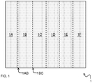
- FIG. 1 schematically shows a thin-film photovoltaic product 1 with a plurality of photovoltaic cells 1A,...,1F.
- the photovoltaic product 1 has a boundary region 1AB, 1BC etc between each pair of a photovoltaic cell and a subsequent photovoltaic cell.
- the photovoltaic product 1 comprises a stack with a bottom electrode layer 12, a top electrode layer 16, and an interface layer 13 and a photovoltaic layer 14 arranged between the first and the top electrode layer.
- Photovoltaic cells 1A, 1B, ....,1F are formed and pairs of a photovoltaic cell 1A and its successor 1B are serially connected in boundary region 1AB.
- the boundary region 1AB is formed with a single trench 20 having a deepened portion 21 protruding through the bottom electrode layer 12, (See also FIG. 5C ).
- an insulating material 31, 33 is deposited at both sides of the single trench 20. The material 31 protrudes into the deepened portion 21 of the trench 20.
- An electrical connection 32 is provided that extends from an end portion of the top electrode layer 16 of the photovoltaic cell 1A to an portion of and end of the bottom electrode layer 12 of the succeeding photovoltaic cell 1B that is free from insulating material 31,33.
- the photovoltaic layer 14 has edges 14a, 14b at the single trench 20 (See FIG.
- the boundary region 1AB is formed with separate P1-, P2- and P3-trenches 21, 22, 23.
- P1-trench 21 protrudes through each of the top electrode layer 16, the photovoltaic layer 14 and the bottom electrode layer 12 and is filled with an insulating material 31.
- P3-trench 23 protrudes through each of the top electrode layer 16 and the photovoltaic layer 14 and may also be filled with an insulating material 33, but this is not mandatory.
- P2-trench 22 protrudes through each of the top electrode layer 16 and the photovoltaic layer 14.
- An electrically conductive material 32 bridges the P1-trench 21 to electrically interconnect a portion of the top electrode layer 16 of the photovoltaic cell 1A with a portion of the bottom electrode layer 12 of the photovoltaic cell 1B succeeding photovoltaic cell 1A at the bottom of a P2-trench 22.
- the photovoltaic layer 14 at the side of photovoltaic module 1A has an edge 14a at the P1-trench 21 that is free from re-solidified and phase changed photovoltaic material.
- the photovoltaic layer 14 at the side of photovoltaic module 1B has an edge 14b at the P3-trench 23 that is free from re-solidified and phase changed photovoltaic material.
- Re-solidified and/or phase changed photovoltaic material would otherwise be present in case these trenches 21, 23 were formed by irradiation at higher energy levels, aiming at a direct removal of the photovoltaic material. Likewise, this may apply for the edges of trench 22, but this is not mandatory, as an electrical connection is formed anyway in this trench.
- the bottom electrode layer 12 at the bottom of the trenches 22, 23 and the remaining portions of the trench 21 are free from scratches as use of a needle can be avoided.
- a method of manufacturing a photovoltaic product 1 as shown in FIG. 1 and FIG. 5E or FIG. 6F may comprise depositing a photovoltaic layer stack, partitioning the stack into photovoltaic modules and serially interconnecting the photovoltaic modules.
- steps may be implemented for example in a roll-to-roll method wherein a foil, e.g. a PET- or PEN foil, serving as a substrate 10 is guided along various manufacturing facilities.
- the manufacturing facilities may be provided in a single production plant but may alternatively be provided at mutually different production locations.
- the various operations of the method are provided batch wise. In that case also a rigid material, such as glass may be used as the substrate.
- the method may for example use a series of manufacturing facilities.
- a first manufacturing facility deposits a stack with a bottom electrode layer 12, a top electrode layer 16 and a photovoltaic layer 14 arranged between said first and said top electrode layer, the bottom electrode layer 12 and the photovoltaic layer 14 have an interface layer 13.
- the interface layer 13 may be provided in an additional deposition step succeeding deposition of the bottom electrode layer 12, and preceding deposition of the photovoltaic layer 14.
- an interface layer may be formed as a result of a chemical interaction between material of the bottom electrode layer 12 and material of the photovoltaic layer 14.
- an interface layer of MoSe 2 may be formed by a chemical reaction at the boundary of a Mo electrode layer and a CIGS photovoltaic layer.
- a second manufacturing facility partitions the photovoltaic layer stack into photovoltaic cells 1A, 1B, etc. As a result of partitioning a boundary region 1AB is formed between each photovoltaic cell 1A and a subsequent photovoltaic cell 1B.
- a third manufacturing facility serially interconnects mutually subsequent photovoltaic cells 1A. 1B in their boundary region 1AB.
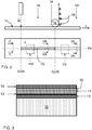
- FIG. 2 schematically shows a side- view of a manufacturing unit which is part of the manufacturing facility in a roll-to-roll manufacturing process. This part serves to form a trench 20 through the top electrode layer 16 and the photovoltaic layer 14 in a hybrid procedure as referred to above. It is presumed that this manufacturing unit receives a substrate 10, e.g. a PET or PEN foil which is already provided with a photovoltaic layer stack .
- a substrate 10 e.g. a PET or PEN foil which is already provided with a photovoltaic layer stack .
- FIG. 3 is a cross-section of the semi-finished product according to III-III in FIG. 2 and shows the semi-finished product in the state wherein it is received by this manufacturing stage.
- the received semi-finished product comprises a bottom electrode layer 12, a top electrode layer 16 and a photovoltaic layer 14 arranged between said first and said top electrode layer.
- an interface layer 13 as referred to above, is present between the bottom electrode layer 12 and the photovoltaic layer 14.Also an interface layer 15 may be present between the photovoltaic layer 14 and the top electrode layer 16.
- this stage comprises an irradiation sub-step S23A followed by a mechanical fragment removal sub-step S23B.
- the irradiation sub-step S23A the semi-finished product is irradiated from a side facing the top electrode layer 16 with a laser beam LB in an irradiation zone Z3 where the trench 20 is to be formed.
- the beam LB with which the zone Z3 is irradiated has a wavelength for which the interface 13 between the bottom electrode layer 12 and the photovoltaic layer 14 has a relatively high absorption as compared to the photovoltaic layer 14 and the top electrode layer 16.
- the interface 13 is heated and causes a local thermally and/or pressure induced stress in the photovoltaic layer 14 and the top electrode layer 16 present thereon.
- a modest absorption of radiation in the photovoltaic layer and top electrode layer e.g. absorption of radiation having a wavelength of 1550 nm in a CIGS type photovoltaic layer, may contribute to its fragmentation without causing a phase change.
- the thermally and/or pressure induced stress causes these layers to locally crack into fragments within the zone Z3, as shown schematically in FIG. 4A , which is a cross-section according to IVA-IVA in FIG. 2 .
- a (partial) evaporation of the interface layer 13 may contribute in pressure induction.
- FIG. 5A is a cross-section according to VA-VA in FIG. 2 , that schematically shows the semi-finished product after this stage. Additionally or alternatively other methods may be applied for mechanical fragment removal, such as tacky rollers, air flow, carbon dioxide snow and the like.
- Samples were prepared on a substrate 10 provided with a bottom electrode layer 12 of Mo with a thickness of 400nm, a copper indium gallium selenide photovoltaic layer 14 having a thickness of 1600 nm and a top electrode layer comprising i -ZnO/AZO TCO 16 having a thickness of 400 nm.
- the irradiation sub-step was performed by irradiating the samples with a pulsed laser beam from an Erbium laser having a power of 0.3 W, a wavelength of 1550 nm and a spotsize of 50 micron.
- the repetition rate was 10 kHz and the pulse duration 2 ns.
- the beam was translated along a partitioning line at a speed of 250 mm/s.
- FIG. 4B is a picture of a sample after the irradiation sub-step, which is taken according to a top-view as indicated by IVB in FIG. 2 . It can be seen in FIG. 4B , that the material of the layers 14, 16 is fragmented in the area Z3 traversed by the laser beam LB, but that the fragmented material is still located at the surface of the sample close to its original location.
- FIG. 5B which is a picture of the sample according to view VB in FIG. 2 clearly shows that the layers 14, 16 are partitioned in sections, each at a respective side of trench 20, each associated with a respective photovoltaic cell 1A, 1B to be formed.
- the variations in width of the trench 20 are relatively small in comparison to the average width of the trench 20. It was confirmed that neither re-solidified material nor phase changed photovoltaic material was present at the edges 14a, 14b of the photovoltaic layer 14 with the trench 20 of the sample so obtained. Sparsely distributed remnants of photovoltaic material are present at the bottom electrode layer 12 at the bottom of the trench 20 of this sample. It was confirmed however that the exposed bottom electrode layer 12 is free from scratches.
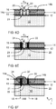
- FIG. 5C-5E show further process steps that may be applied to the semi-finished product of FIG. 5A .
- FIG. 5C it is shown how the trench 20 is provided with a deepened portion 21.
- the deepened portion 21 extends at distance from the edges of the trench 20, in its length direction and therewith partitions the bottom electrode layer 12 into mutually insulated parts at each side of the deepened portion 21.
- Various methods are suitable to form this deepened portion 21, e.g. mechanical removal of the material of the bottom electrode layer 12 with a needle, laser ablation and the like. Due to the fact that the deepened portion 21 is formed at distance from the edges 14a and 14b of the trench 20 it can be avoided that therewith the photovoltaic material at these edges is heated to the extent that it melts or that a phase change occurs.
- FIG. 5D it is shown, how an insulating material 31, 32, typically, but not necessarily the same insulating material, is deposited at both sides of the single trench 20. Therewith the material 31 protrudes into the deepened portion 21 of the trench 20 and a strip 12ab of the bottom electrode layer 12 remains exposed between the deposited insulating material 31, 32.
- an insulating material 31, 32 typically, but not necessarily the same insulating material
- FIG. 5E it is shown how an electrical connection 32 is provided by deposition of an electrically conductive material.
- the electrical connection 32 formed therewith extends from an end portion of the top electrode layer 16 of the photovoltaic cell 1A to the exposed strip 12ab of the bottom electrode layer 12 of the succeeding photovoltaic cell 1B.
- FIG. 6A-6F show another example, wherein the herein disclosed hybrid procedure is applied as part of a series of further processing steps to form a plurality of serially interconnected photovoltaic modules.
- FIG. 6A shows a semi-finished product comprising a bottom electrode layer 12, a top electrode layer 16 and a photovoltaic layer 14 arranged between the first and said top electrode layer.
- the bottom electrode layer 12 and the photovoltaic layer 14 have an interface layer 13.
- the semi-finished product in FIG. 6A was provided with a P1-trench 20 using the above-mentioned hybrid procedure.
- the trench 20 was further provided with a deepened portion 21 to partition the bottom electrode layer 12 for example with an irradiation step S21C using a pulsed laser LB2. Due to the fact that the hybrid procedure was used to form the trench 20, and the fact that the deepened portion 21 is narrower than the trench 20, too high temperatures of the photovoltaic material 14a near the wall of the trench 20 can be avoided, therewith avoiding that it rendered conductive.
- a P3-trench 23 at a distance d 13 from the P1-trench 20, 21 was provided using the above-mentioned hybrid procedure. By using this hybrid procedure it was also avoided that photovoltaic material 14b near the wall of the trench 23 was rendered conductive.
- a P2-trench 22 was provided with the herein disclosed hybrid procedure, at a distance d 12 from the P1-trench 20, 21, between the P1-trench and the P3-trench. It is advantageous to also use the hybrid procedure to form the P2-trench, so that only a single set of process parameters (except for the additional step to form deepened portion 21 in trench 20) needs to be set for all trenches.
- the P2-trench 22 may also be formed in other ways as it is not a problem when the photovoltaic material near the P2-trench is rendered conductive. This is because the P2-trench serves as the passage for an electrical connection between the photovoltaic modules to be formed.
- FIG. 6D shows a further stage, wherein the P1-trench 20, 21 and the P3-trench 23 are filled with an insulating material 31, 33 respectively.
- the filling 31, 33 makes it easier to avoid shortcuts in later manufacturing stages, for example the further stage shown in FIG. 6C .
- an electrical connection 32 is formed between a portion of the top electrode layer 16 of the first photovoltaic cell 1A and a portion of the bottom electrode layer 12 of the second photovoltaic cell 1B in P2-trench 22.
Landscapes
- Photovoltaic Devices (AREA)
- Engineering & Computer Science (AREA)
- Life Sciences & Earth Sciences (AREA)
- Sustainable Energy (AREA)
- Manufacturing & Machinery (AREA)
Priority Applications (5)
| Application Number | Priority Date | Filing Date | Title |
|---|---|---|---|
| EP19187042.7A EP3767686A1 (de) | 2019-07-18 | 2019-07-18 | Herstellungsverfahren eines fotovoltaischen dünnschichtbauelements |
| CN202080051711.5A CN114127958B (zh) | 2019-07-18 | 2020-07-17 | 制造薄膜光伏产品的方法 |
| PCT/NL2020/050473 WO2021010837A1 (en) | 2019-07-18 | 2020-07-17 | Method of manufacturing a thin-film photovoltaic product |
| US17/625,564 US11749765B2 (en) | 2019-07-18 | 2020-07-17 | Method of manufacturing a thin-film photovoltaic product |
| EP20743378.0A EP4000105B1 (de) | 2019-07-18 | 2020-07-17 | Herstellungsverfahren eines fotovoltaischen dünnschichtbauelements |
Applications Claiming Priority (1)
| Application Number | Priority Date | Filing Date | Title |
|---|---|---|---|
| EP19187042.7A EP3767686A1 (de) | 2019-07-18 | 2019-07-18 | Herstellungsverfahren eines fotovoltaischen dünnschichtbauelements |
Publications (1)
| Publication Number | Publication Date |
|---|---|
| EP3767686A1 true EP3767686A1 (de) | 2021-01-20 |
Family
ID=67438010
Family Applications (2)
| Application Number | Title | Priority Date | Filing Date |
|---|---|---|---|
| EP19187042.7A Withdrawn EP3767686A1 (de) | 2019-07-18 | 2019-07-18 | Herstellungsverfahren eines fotovoltaischen dünnschichtbauelements |
| EP20743378.0A Active EP4000105B1 (de) | 2019-07-18 | 2020-07-17 | Herstellungsverfahren eines fotovoltaischen dünnschichtbauelements |
Family Applications After (1)
| Application Number | Title | Priority Date | Filing Date |
|---|---|---|---|
| EP20743378.0A Active EP4000105B1 (de) | 2019-07-18 | 2020-07-17 | Herstellungsverfahren eines fotovoltaischen dünnschichtbauelements |
Country Status (4)
| Country | Link |
|---|---|
| US (1) | US11749765B2 (de) |
| EP (2) | EP3767686A1 (de) |
| CN (1) | CN114127958B (de) |
| WO (1) | WO2021010837A1 (de) |
Cited By (2)
| Publication number | Priority date | Publication date | Assignee | Title |
|---|---|---|---|---|
| CN113421950A (zh) * | 2021-06-21 | 2021-09-21 | 安徽华晟新能源科技有限公司 | 太阳能电池片的制造方法 |
| US20220293805A1 (en) * | 2019-07-18 | 2022-09-15 | Nederlandse Organisatie Voor Toegepast-Natuurwetenschappelijk Onderzoek Tno | Method of manufacturing a thin-film photovoltaic product |
Families Citing this family (2)
| Publication number | Priority date | Publication date | Assignee | Title |
|---|---|---|---|---|
| WO2025094721A1 (ja) * | 2023-10-31 | 2025-05-08 | 富士フイルム株式会社 | 太陽電池の製造方法 |
| DE102023134364A1 (de) * | 2023-12-07 | 2025-06-12 | acp systems AG | Verfahren zum Herstellen einer verformbaren Photovoltaik-Einheit, Verfahren zum Herstellen einer verformbaren Photovoltaik-Reihe, verformbare Photovoltaik-Einheit, verformbare Photovoltaik Reihe, verformbares Photovoltaik-Modul |
Citations (4)
| Publication number | Priority date | Publication date | Assignee | Title |
|---|---|---|---|---|
| US20120094425A1 (en) * | 2010-10-14 | 2012-04-19 | Miasole | Ablative scribing of solar cell structures |
| JP2012169569A (ja) * | 2011-02-17 | 2012-09-06 | Kyocera Corp | 光電変換装置の製造方法 |
| WO2013026463A1 (en) | 2011-08-19 | 2013-02-28 | Universita' Degli Studi Di Padova | Laser scribing process |
| US20160126376A1 (en) * | 2014-10-31 | 2016-05-05 | Korea Institute Of Science And Technology | Method for manufacturing thin film solar cell and module structure of thin film solar cell |
Family Cites Families (11)
| Publication number | Priority date | Publication date | Assignee | Title |
|---|---|---|---|---|
| US20110030758A1 (en) * | 2009-08-07 | 2011-02-10 | Sanyo Electric Co., Ltd. | Photovoltaic device and manufacturing method thereof |
| KR20120003213A (ko) * | 2010-07-02 | 2012-01-10 | 삼성전자주식회사 | 태양 전지 모듈 및 그 제조 방법 |
| FR2972299B1 (fr) * | 2011-03-01 | 2016-11-25 | Commissariat Energie Atomique | Procédé pour la mise en série électrique monolithique de cellules photovoltaïques d'un module solaire et module photovoltaïque mettant en œuvre ce procédé |
| CN103283006A (zh) * | 2011-11-07 | 2013-09-04 | 松下电器产业株式会社 | 薄膜晶体管器件的制造方法、薄膜晶体管器件以及显示装置 |
| FR2989223B1 (fr) * | 2012-04-06 | 2014-12-26 | Commissariat Energie Atomique | Procede pour realiser un module photovoltaique avec une etape de gravure p3 et une eventuelle etape p1. |
| DE102012205978A1 (de) * | 2012-04-12 | 2013-10-17 | Robert Bosch Gmbh | Photovoltaische Dünnschichtsolarmodule sowie Verfahren zur Herstellung solcher Dünnschichtsolarmodule |
| NL2016708B1 (en) * | 2016-04-29 | 2017-11-16 | Stichting Energieonderzoek Centrum Nederland | A method for manufacturing interconnected solar cells and such interconnected solar cells. |
| FR3082356B1 (fr) * | 2018-06-11 | 2020-06-19 | Armor | Procede de fabrication d'un module photovoltaique et module photovoltaique ainsi obtenu |
| EP3654389A1 (de) * | 2018-11-16 | 2020-05-20 | Nederlandse Organisatie voor toegepast- natuurwetenschappelijk onderzoek TNO | Fotovoltaische vorrichtung und verfahren zur herstellung davon |
| EP3764405A1 (de) * | 2019-07-10 | 2021-01-13 | Nederlandse Organisatie voor toegepast- natuurwetenschappelijk Onderzoek TNO | Verfahren zur herstellung eines fotovoltaischen dünnschichtprodukts |
| EP3767686A1 (de) * | 2019-07-18 | 2021-01-20 | Nederlandse Organisatie voor toegepast- natuurwetenschappelijk Onderzoek TNO | Herstellungsverfahren eines fotovoltaischen dünnschichtbauelements |
-
2019
- 2019-07-18 EP EP19187042.7A patent/EP3767686A1/de not_active Withdrawn
-
2020
- 2020-07-17 CN CN202080051711.5A patent/CN114127958B/zh active Active
- 2020-07-17 US US17/625,564 patent/US11749765B2/en active Active
- 2020-07-17 EP EP20743378.0A patent/EP4000105B1/de active Active
- 2020-07-17 WO PCT/NL2020/050473 patent/WO2021010837A1/en not_active Ceased
Patent Citations (4)
| Publication number | Priority date | Publication date | Assignee | Title |
|---|---|---|---|---|
| US20120094425A1 (en) * | 2010-10-14 | 2012-04-19 | Miasole | Ablative scribing of solar cell structures |
| JP2012169569A (ja) * | 2011-02-17 | 2012-09-06 | Kyocera Corp | 光電変換装置の製造方法 |
| WO2013026463A1 (en) | 2011-08-19 | 2013-02-28 | Universita' Degli Studi Di Padova | Laser scribing process |
| US20160126376A1 (en) * | 2014-10-31 | 2016-05-05 | Korea Institute Of Science And Technology | Method for manufacturing thin film solar cell and module structure of thin film solar cell |
Cited By (3)
| Publication number | Priority date | Publication date | Assignee | Title |
|---|---|---|---|---|
| US20220293805A1 (en) * | 2019-07-18 | 2022-09-15 | Nederlandse Organisatie Voor Toegepast-Natuurwetenschappelijk Onderzoek Tno | Method of manufacturing a thin-film photovoltaic product |
| US11749765B2 (en) * | 2019-07-18 | 2023-09-05 | Nederlandse Organisatie Voor Toegepast-Natuurwetenschappelijk Onderzoek Tno | Method of manufacturing a thin-film photovoltaic product |
| CN113421950A (zh) * | 2021-06-21 | 2021-09-21 | 安徽华晟新能源科技有限公司 | 太阳能电池片的制造方法 |
Also Published As
| Publication number | Publication date |
|---|---|
| WO2021010837A1 (en) | 2021-01-21 |
| CN114127958B (zh) | 2024-08-09 |
| CN114127958A (zh) | 2022-03-01 |
| EP4000105C0 (de) | 2025-01-08 |
| US11749765B2 (en) | 2023-09-05 |
| EP4000105B1 (de) | 2025-01-08 |
| US20220293805A1 (en) | 2022-09-15 |
| EP4000105A1 (de) | 2022-05-25 |
Similar Documents
| Publication | Publication Date | Title |
|---|---|---|
| EP4000105B1 (de) | Herstellungsverfahren eines fotovoltaischen dünnschichtbauelements | |
| FI117608B (fi) | Menetelmä ohutkalvoaurinkokennojen integroidun laserstrukturoinnin tekemiseksi | |
| CN106687617B (zh) | 激光转印ibc太阳能电池 | |
| US11869993B2 (en) | Method of manufacturing a thin film photovoltaic product | |
| Jamaatisomarin et al. | Laser scribing of photovoltaic solar thin films: A review | |
| Franta et al. | Simultaneous high crystallinity and sub-bandgap optical absorptance in hyperdoped black silicon using nanosecond laser annealing | |
| US9831363B2 (en) | Laser epitaxial lift-off of high efficiency solar cell | |
| US8048706B1 (en) | Ablative scribing of solar cell structures | |
| Bayer et al. | Morphology and topography of perovskite solar cell films ablated and scribed with short and ultrashort laser pulses | |
| PT1319254E (pt) | Método para a produção de um contacto metálico semicondutor atrvés de uma camada dieléctrica. | |
| WO2012051574A2 (en) | Ablative scribing of solar cell structures | |
| CN102763220B (zh) | 用于至少局部地除去层堆叠的层的方法 | |
| Hwang et al. | Laser scribing of CIGS thin-film solar cell on flexible substrate | |
| Turan et al. | Cost‐effective absorber patterning of perovskite solar cells by nanosecond laser processing | |
| JP2013258405A (ja) | 下層からのコーティングの選択的および/または高速化除去ならびにその太陽電池への適用 | |
| Lemke et al. | Picosecond laser induced selective removal of functional layers on CIGS thin film solar cells | |
| CN109643740A (zh) | 制造互连太阳能电池的方法及这种互连太阳能电池 | |
| Canteli et al. | Picosecond-laser structuring of amorphous-silicon thin-film solar modules | |
| Kuk et al. | Effect of nanosecond laser beam shaping on Cu (In, Ga) Se2 thin film solar cell scribing | |
| KR101385235B1 (ko) | 레이저 스크라이빙 기술을 이용한 투명전도막 미세 패터닝 방법 | |
| JP2009239281A (ja) | 光起電モジュールの酸化亜鉛製の前側電極層をパターン加工するための方法 | |
| Suryavanshi et al. | Nanosecond pulse fiber laser patterning of bilayer molybdenum thin film on 2-sq inch soda-lime glass substrate for CIGS thin film solar cell applications | |
| JP2005527858A (ja) | 電気光学システムのレーザー構造化 | |
| US8021911B2 (en) | Method for producing a photovoltaic module | |
| Rekow et al. | Micromachining PV materials with time domain tailored laser pulses |
Legal Events
| Date | Code | Title | Description |
|---|---|---|---|
| PUAI | Public reference made under article 153(3) epc to a published international application that has entered the european phase |
Free format text: ORIGINAL CODE: 0009012 |
|
| STAA | Information on the status of an ep patent application or granted ep patent |
Free format text: STATUS: THE APPLICATION HAS BEEN PUBLISHED |
|
| AK | Designated contracting states |
Kind code of ref document: A1 Designated state(s): AL AT BE BG CH CY CZ DE DK EE ES FI FR GB GR HR HU IE IS IT LI LT LU LV MC MK MT NL NO PL PT RO RS SE SI SK SM TR |
|
| AX | Request for extension of the european patent |
Extension state: BA ME |
|
| STAA | Information on the status of an ep patent application or granted ep patent |
Free format text: STATUS: THE APPLICATION IS DEEMED TO BE WITHDRAWN |
|
| 18D | Application deemed to be withdrawn |
Effective date: 20210721 |