EP3768048B1 - Réacteur plasma de décharge à barrière diélectrique et procédé d'évaporation sous vide amélioré au plasma - Google Patents
Réacteur plasma de décharge à barrière diélectrique et procédé d'évaporation sous vide amélioré au plasma Download PDFInfo
- Publication number
- EP3768048B1 EP3768048B1 EP19187406.4A EP19187406A EP3768048B1 EP 3768048 B1 EP3768048 B1 EP 3768048B1 EP 19187406 A EP19187406 A EP 19187406A EP 3768048 B1 EP3768048 B1 EP 3768048B1
- Authority
- EP
- European Patent Office
- Prior art keywords
- electrode
- face
- barrier discharge
- plasma reactor
- dielectric barrier
- Prior art date
- Legal status (The legal status is an assumption and is not a legal conclusion. Google has not performed a legal analysis and makes no representation as to the accuracy of the status listed.)
- Active
Links
Images





Classifications
-
- H—ELECTRICITY
- H05—ELECTRIC TECHNIQUES NOT OTHERWISE PROVIDED FOR
- H05H—PLASMA TECHNIQUE; PRODUCTION OF ACCELERATED ELECTRICALLY-CHARGED PARTICLES OR OF NEUTRONS; PRODUCTION OR ACCELERATION OF NEUTRAL MOLECULAR OR ATOMIC BEAMS
- H05H1/00—Generating plasma; Handling plasma
- H05H1/24—Generating plasma
- H05H1/2406—Generating plasma using dielectric barrier discharges, i.e. with a dielectric interposed between the electrodes
Definitions
- the invention is related to a dielectric barrier discharge (DBD) plasma reactor. More specifically, the DBD plasma reactor according to the invention is a device suitable for plasma-enhanced chemical vapor deposition (PECVD) of a coating, for example a crystalline inorganic coating, on a substrate under atmospheric pressure conditions. Examples of crystalline inorganic coatings are V 2 O 5 and TiO 2 .
- the invention is also related to a method for performing PECVD. More precisely, a PECVD method for forming a coating, for example a crystalline inorganic coating, on a substrate under atmospheric pressure conditions.
- a known option for forming crystalline inorganic coatings is the use of a two-step process wherein in a first step quasi-amorphous films are deposited followed by a second annealing step.
- a DBD plasma reactor operating at atmospheric pressure and room temperature e.g. 25°
- room temperature e.g. 25°
- the DBD plasma reactor is a device that comprises a first electrode, a second electrode separated from the first electrode, and a first dielectric layer located between the first and the second electrode.
- a plasma area is formed between the first and the second electrode and the substrate is placed in the plasma area.
- a main gas and generally also a precursor under gaseous form, are introduced between the two electrodes and a power supply is used to apply a voltage, generally an alternating voltage, between the first electrode and the second electrode and create a plasma in the plasma area.
- an annealing process needs to be started, i.e. the substrate needs to be heated after deposition until it reaches a sufficiently high temperature for the coating to recrystallize and take a specific crystalline form.
- FIG 3 shows a device for coating the outer surface of a welding wire continuously moving through a tube comprising a dielectric barrier discharge (DBD) plasma reactor wherein a coating material is introduced in vapor form for deposition on the outer surface of the welding wire.
- the coating material is an alkali metal.
- Such coating material doesn't require annealing and therefore doesn't need to be heated after its deposition.
- Fig 12 shows another embodiment wherein the welding wire passes through a middle portion of the device which does not comprise electrodes and where the wire is heated by a magnetic field generated by a coil arranged coaxially around the wire.
- the welding wire need to be heated before passing through the next portion of the device, it is anyway heated outside of any plasma area.
- the substrate the welding wire therefore has to be moved outside of the plasma area in order to be heated, which necessarily takes time.
- Patent document KR101507383B1 discloses a similar arrangement where the coating and heating steps are separated.
- a disadvantage of these approaches is that the overall processing time is long as the annealing step can take hours before completion.
- Patent document JP2006032303A discloses a capacitive-inductive plasma generation. It has no electrodes and is therefore not capable to produce a DBD plasma.
- Patent document US5510158A discloses a device comprising a DBD reactor. However, the substrate is not placed in the plasma area of the DBD reactor and it is merely by light created by the excited plasma that the substrate is treated.
- the substrate could be heated by resistive heating during the deposition.
- resistive heating is often hard to realize in real experimental conditions, as most of the atmospheric plasma deposition is done using high-frequency dielectric barrier discharge, typically in the 1kHz to 100 kHz range.
- One of the problems is electrical interference between the heating circuit and the plasma circuit, and a further difficulty is related to efficiently heating a substrate when a dielectric is located between the substrate and the electrode. In practice, when using resistive heating, the entire reactor with the electrodes and dielectric is being heated resulting in high power consumption.
- a further object is to reduce the overall power consumption of the DBD plasma reactor and reduce the overall processing time for forming the coating.
- a dielectric barrier discharge (DBD) plasma reactor for plasma enhanced chemical vapor deposition of a coating on a substrate under atmospheric pressure is provided.
- DBD dielectric barrier discharge
- the DBD plasma reactor comprises a first electrode having a first face and a second face opposite to the first face, a second electrode having a third and a fourth face opposite to the third face, the fourth face of the second electrode facing the second face of the first electrode, and wherein the second electrode is separated from the first electrode for forming a plasma area between the second face and the fourth face.
- the DBD plasma reactor further comprises a first dielectric layer covering the second face of the first electrode and a power supply configured to apply a voltage between the first and second electrode.
- the DBD plasma reactor is characterized in that the plasma reactor further comprises an induction heating coil for heating by induction a substrate when placed in the plasma area and/or for heating a susceptor by induction when placed in the plasma area.
- the induction heating coil is located outside of the plasma area and the induction heating coil comprises a plurality of windings winded around a central coil axis.
- the induction heating coil is for example located such that the first face of the first electrode is facing the induction heating coil or the third face of the second electrode is facing the induction heating coil.
- the DBD plasma reactor is further characterized in that the first electrode and/or second electrode comprises at least a through-hole extending along the central coil axis.
- magnetic field lines generated along the coil axis are passing through the through-hole for crossing the first electrode.
- the heating of the first electrode by induction is reduced and when a susceptor is placed on the first dielectric layer, mainly the susceptor is heated by induction.
- overall power consumption for heating the substrate is reduced.
- the DBD plasma reactor further comprises, in addition to the first dielectric layer, a second dielectric layer covering the fourth face of the second electrode.
- a second dielectric layer covering the fourth face of the second electrode.
- At least a central portion of the second face and a central portion of the fourth face are planar and parallel. If for example the second face is planar, this facilitates positioning a susceptor or a substrate on top of the dielectric covering the second face.
- the plurality of windings of the induction heating coil are forming a helix-type coil extending along the central coil axis.
- magnetic field lines are extending and concentrated along the central coil axis and are passing through the through-hole in the first electrode.
- the first electrode comprises a slit for suppressing Eddy currents generated in the first electrode.
- the slit is extending from an inner perimeter delimiting the through-hole of the first electrode to an outer perimeter of the first electrode.
- closed circuits of Eddy currents formed in a plane of the first electrode are broken such that heating of the electrode by Eddy currents is avoided.
- the slit is not entirely extending from the inner perimeter to the outer perimeter, but is only extending over a limited distance.
- the plurality of windings of the induction heating coil are located in a plane for forming a pancake-type coil.
- the ratio between a thickness of the first electrode and a skin depth of the first electrode is smaller than 1, preferably smaller than 0.5, more preferably smaller than 0.1. In this way, induction heating of the first electrode is strongly reduced.
- the ratio between a thickness (S) of the second electrode and a skin depth ( ⁇ ) of the second electrode is smaller than 1, preferably smaller than 0.5, more preferably smaller than 0.1.
- both the first and second electrode fulfill this condition.
- the induction heating coil comprises a magnetic core, preferably a ferrite core.
- the coating is a crystalline inorganic coating, more preferably comprising a transition metal oxide.
- the DBD plasma reactor is especially suited for crystalline coating, such as for example V 2 O 5 and TiO 2 , that is performed at atmospheric pressure and room temperature.
- the substrate is directly or indirectly heated by the induction heating coil, no additional step of annealing is needed.
- the DBD plasma reactor comprises a gas injection system configured to introduce a gas into the plasma area.
- a precursor in a gaseous form is also injected in the plasma area by the gas injection system.
- the DBD plasma reactor comprises a susceptor, generally arranged on the first dielectric layer.
- a susceptor is to be construed as a piece of material, such as a layer or plate of material configured such that the substrate can be arranged on the susceptor for forming a thermal contact between the susceptor and the substrate.
- the susceptor when the DBD plasma reactor is in operation, the susceptor is heated by induction by the induction heating coil and a substrate in thermal contact with the susceptor will be heated by thermal conduction.
- the susceptor is made of a metal, more preferably the susceptor is made of a ferromagnetic metal or a ferromagnetic alloy.
- the central coil axis of the induction heating coil is crossing the susceptor.
- a method for forming a coating, preferably a crystalline inorganic coating, on a substrate using PECVD under atmospheric pressure conditions is provided as defined in the appended claims.
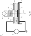
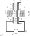
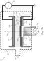
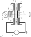
- Fig.1a to Fig.1d and Fig.2a to Fig.2c examples of embodiments of dielectric barrier discharge (DBD) plasma reactors 1 for plasma enhanced chemical vapor deposition of a coating on a substrate under atmospheric pressure according to the present invention as defined by the claims are shown.
- DBD dielectric barrier discharge
- Such a DBD plasma reactor 1 comprises a first electrode 11 separated from a second electrode 12.
- the first electrode 11 has a first face 11a and a second face 11b opposite to the first face 11a
- the second electrode 12 has a third 12a and a fourth face 12b, opposite to the third face.
- the fourth face 12b of the second electrode is facing the second face 11b of the first electrode.
- the first electrode is for example a ground electrode and the second electrode is a high-voltage electrode and a voltage can be applied between the first and second electrode with a power supply 30.
- the voltage applied between the first and the second electrode is a direct pulsed voltage.
- the electrodes are made of a good conducting material, such as for example copper or aluminum.
- the fact that the second face 11b and the fourth face 12b are facing each other does not imply that no other elements are placed between the two faces.
- one or more dielectric layers or additionally a susceptor can for example be placed between the second face 11b and the fourth face 12b.
- the DBD plasma reactor 1 shown on Fig.1a and Fig.1b comprises a first dielectric layer 21 covering the second face 11b of the first electrode.
- the DBD plasma reactor according to the invention is characterized in that it comprises an induction heating coil 40 for heating by induction a substrate when placed in the plasma area 62 and/or for heating a susceptor by induction when placed in the plasma area 62.
- induction heating coil 40 for heating by induction a substrate when placed in the plasma area 62 and/or for heating a susceptor by induction when placed in the plasma area 62.
- reference 100 schematically illustrates a susceptor that is located on top of the first dielectric layer 21.
- the substrate is directly positioned on the first dielectric layer 21 without use of a susceptor.
- the induction heating coil is located outside of the plasma area.
- the first face 11a of the first electrode is facing the inducting heating coil 40.
- the induction heating coil 40 is placed under the first electrode.
- the induction heating coil is placed on top of the second electrode.
- the third face 12a of the second electrode is facing the induction heating coil 40.
- the induction heating coil 40 is a coil comprising a plurality of windings winded around a central coil axis X B .
- the induction heating coil is powered by a power supply 50 for providing an alternating current in the coil, typically at a frequency in the kHz range, for example a frequency in range between 1 kHz and 100 kHz.
- the DBD reactor according to the present invention is not limited to embodiments having only one induction heating coil. Indeed, in some embodiments the DBD reactor comprises more than one induction heating coil. For example, as schematically illustrated on Fig.1d and Fig.2c , two induction heating coils 40a and 40b are provided having a common central axis X B .
- the DBD plasma reactor according to the invention is further characterized in that the first electrode 11 and/or the second electrode 12 comprises a through-hole 15 extending along the central coil axis X B .
- the first electrode 11 and/or the second electrode 12 comprises a through-hole 15 extending along the central coil axis X B .
- Fig.1a and Fig.2a examples are shown of embodiments wherein the first electrode comprises a through-hole while Fig.1b shows an example wherein the through-hole is made in the second electrode.
- Fig.1c and Fig.2b examples of embodiments are shown wherein both the first 11 and the second 12 electrode comprise a through-hole 15. The role of the through-hole 15 will be further discussed.
- the DBD plasma reactor of the current invention is not limited to one dielectric layer.
- Fig.2a and Fig.2b embodiments of a reactor are shown comprising a second dielectric layer 22 covering the fourth face 12b of the second electrode 12.
- the DBD plasma reactor is suitable to operate under atmospheric pressure, which is to be construed as operating in pressure ranges between 100 torr and 1000 torr.
- a DBD plasma reactor comprises a gas injection system configured to introduce gases into the plasma area.
- a main gas such as e.g. argon, or helium or any other noble gas
- the word "main gas” is used in order to distinguish the noble gas from other additional gases that could be introduced in the plasma area.
- a precursor under gaseous form is introduced into the plasma area.
- a chamber 60 is used that is containing at least the first electrode, the second electrode and the induction heating coil.
- a gas inlet 61 is generally provided to supply gas to the chamber.
- the arrow on Fig.2a schematically indicates a gas flow direction when entering the chamber.
- no chamber is required when for example the DBD plasma reactor is located in an atmospheric pressure controlled environment and wherein a gas can directly be introduced in the plasma area.
- the power supply 30 for the electrodes is commercially available and is for example supplying an alternating voltage, e.g. generating an alternating voltage in the kHz range, for example a frequency between 1 and 30 kHz. In other embodiments, the power supply provides a pulsed DC voltage.
- a central portion of the first electrode 11 and a central portion of the second electrode 12 are planar and parallel.
- the electrodes do not necessarily have portions that are planar and/or parallel.
- the second face of the first electrode and the fourth face of the second electrode are planar and/or parallel.
- the first and/or second electrode is/are made of non-magnetic metals.
- the magnetic field lines pass through the metal plate longitudinally, in a plane parallel with the metal plate.
- the induced Eddy currents will flow through the thickness of the metal plate in small loops as schematically illustrated on Fig.3b .
- the skin depth ⁇ being the thickness used by the current to flow, also plays a role when designing the first electrode and/or the susceptor as will be further explained below.
- the equation defining the skin depth is well known in the art and the skin depth ⁇ depends on the frequency of the varying magnetic field inducing the Eddy currents and on the electrical conductivity and magnetic permeability of the material wherein the Eddy currents are induced.
- the DBD plasma reactor comprises a susceptor.
- a susceptor to achieve a good heating of any kind of substrate, either metallic or non-metallic, it is preferred to add a metallic component placed under the substrate that will be uniformly heated by induction.
- This metallic component is called the "susceptor”.
- This susceptor can be made of any kind of metal, but a ferromagnetic metal like nickel or iron will be far more susceptible to induction heating than a non-ferromagnetic metal like copper or aluminum, due to the contribution of the magnetic permeability to the skin depth and the hysteresis losses.
- the electric resistance of the conductor is also important as a high resistance metal will heat faster than a low resistance metal due to Joule effect.
- the susceptor will be a thin sheet or grid of ferromagnetic metal preferably with high resistance. It should withstand a high temperature without oxidation, melting or chemical modification. Suitable materials are Iron, Nickel, Cobalt and any other ferromagnetic alloy with a high Curie temperature and with a reasonable resistance.
- the substrate is a conducting material, it is not absolutely necessary to use an additional susceptor and the substrate can for example directly be placed on top of the first dielectric layer for being heated by induction by the induction heating coil.
- the induction heating coil 40 that is schematically shown on Fig.1a to Fig.1c , Fig.2a and Fig.2b is a coil wherein the plurality of windings are forming a so-called helix-type coil extending along the central coil axis X B .
- This type of coil can also be named solenoid shaped coil.
- the windings are typically made with Litz wire.
- the magnetic field lines are similar to the magnetic field lines shown on Fig.3a , i.e. the magnetic field lines are crossing the first electrode in a direction parallel with the central coil axis. If the first electrode would not have the through-hole 15, the first electrode would be heated by the induced Eddy currents circulating in the first electrode. By providing the through-hole 15 in the first electrode, the magnetic field lines are passing through the through-hole 15, thereby avoiding or reducing induction heating in the first electrode.
- the person skilled in the art will design the dimension of the opening of the through-hole 15 in accordance with the dimension of the induction heating coil. If the through-hole has a circular opening, the diameter can for example be chosen to be equal or slightly larger than an external dimeter of a solenoid shaped coil used as induction coil, as schematically shown on Fig.1a and Fig.2a .
- a through-hole 15 is provided in each of the two electrodes.
- the induction current in the first electrode can be further reduced or eliminated by providing a slit 14 in the electrode.
- the slit 14 is extending from an inner perimeter delimiting the through-hole 15 of the first electrode to an outer perimeter of the first electrode 11.
- the slit brakes the closed electrical circuit when formed in the first electrode such that no circular Eddy currents can circulate.
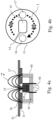
- a slit 14 is schematically shown on Fig.4b for an embodiment wherein the through-hole 15 has a rounded square shape. The two crosses on Fig.4b schematically illustrate that due to the slit 14 no Eddy currents I can circulate as the closed circuit is broken by the slit 14.
- the induction heating coil 40 comprises a magnetic core 41, for example a ferrite core.
- a magnetic core 41 for example a ferrite core.
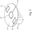
- additional holes 16,17 are made in the first electrode 11. The location of these additional holes match with corresponding components of the magnetic core 41.
- the additional holes 16,17 are also shown on Fig.4b which is a top view of the electrode shown on Fig.4a . This is further illustrated on Fig.5 where a perspective view is shown of the first electrode 11 and part of the ferrite core 41 shown on Fig.4a .
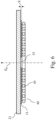
- the DBD plasma reactor is using a pancake-type of induction coil as schematically shown on Fig.6 .
- Fig.6 the first electrode 11, the first dielectric layer 21 and the induction coil 40 of the pancake-type are shown.
- a pancake-type of coil also named flat coil, is a coil wherein the plurality of windings of the coil around a central coil axis X B are located in a plane. This type of pancake coil allows to generate longitudinal field lines, similar to field lines shown on Fig.3b , in a susceptor arranged on the first dielectric layer 21.
- the magnetic field lines of a pancake-type coil are not completely longitudinal and in the center along the central coil axis X B , the magnetic field lines are aligned in the direction of the central coil axis X B and hence these transverse magnetic field lines have to cross through the first electrode before reaching the susceptor. Therefore, for the same reasons as discussed above for the helix-type coil, also for the pancake-type coil, a through-hole 15 extending along the central common coil axis X B is provided in the first electrode 11 in order to avoid or reduce Eddy currents in the plane of the first electrode induced by a varying transverse magnetic field.
- the heating of the first electrode by Eddy currents resulting from the varying longitudinal magnetic field, as illustrated on Fig.3b can be strongly reduced or avoided by selecting the thickness S of the first electrode in relation to the skin depth. Indeed, it is known, that if the ratio S/ ⁇ between the thickness S of the conductor and the skin depth ⁇ is below 2, the power efficiency of the induction heating drops drastically. This is described in for example the publication " Induction heating of thin slabs and sheets in the rolling line", D. Wohlfahrt and R. Jürgens, in 51st Internationalesticianliches Kolloquium Technische (2015) Ilmenau September 11 - 15, 2006 . In other words, if the metal thickness of the first electrode is selected such that the ratio S/ ⁇ is well below 2, the induction heating power is nearly zero and the first electrode will not be heated up.
- the ratio between the thickness S of the first electrode and the skin depth ⁇ of the first electrode is smaller than 1, preferably smaller than 0.5, more preferably equal or smaller than 0.1.
- the material selected for the first electrode is important as the material needs to have on the one hand a good conductivity and on the other hand have a low magnetic permeability.
- the electrode needs at the same time to be a good conductor for the high voltage and also have a low ratio S/ ⁇ , preferably have a skin depth of for example five times or ten time larger than the thickness S of the electrode.
- Usual non-magnetic metals like copper, aluminum and silver have approximatively the same skin depth and need to be 1 ⁇ m thick or thinner to avoid any induction heating with 100 kHz current frequency.
- Carbon graphite is a good alternative as it has an anisotropic conductivity that reduces the skin depth to some millimeters but keeping a good conductivity.
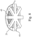
- the pancake-type of induction coil also comprises a magnetic core 41, e.g. made of ferrite or another magnetic material, configured such that the magnetic field lines are bent and concentrated in the region where the induction heating is needed, i.e. at the location where the susceptor and/or the substrate are positioned.
- Magnetic fields lines resulting from the pancake-induction coil are schematically shown as dotted lines on Fig.7 .
- a method for plasma-enhanced chemical vapor deposition of a coating on a substrate under atmospheric pressure using a dielectric barrier discharge plasma reactor as discussed above is provided.
- the coating is a crystalline inorganic coating.
- two methods can be distinguished, depending on if the substrate is conductive or not.
- the method for plasma-enhanced chemical vapor deposition of a coating on a substrate comprises steps of:
- the method for plasma-enhanced chemical vapor deposition of a coating on a substrate comprises steps of:
Landscapes
- Physics & Mathematics (AREA)
- Engineering & Computer Science (AREA)
- Plasma & Fusion (AREA)
- Spectroscopy & Molecular Physics (AREA)
- Plasma Technology (AREA)
Claims (15)
- Réacteur plasma à décharge à barrière électrique (1) pour le dépôt chimique en phase vapeur amélioré et par plasma d'un revêtement sur un substrat sous pression atmosphérique, comprenant:• une première électrode (11) ayant une première face (11a) et une seconde face (11b) opposée à la première face (11a),• une deuxième électrode (12) ayant une troisième face (12a) et une quatrième face (12b) opposée à la troisième face, la quatrième face (12b) de la deuxième électrode faisant face à la deuxième face (11b) de la première électrode, et dans laquelle la deuxième électrode est séparée de la première électrode (11) pour former une zone de plasma (62) entre la deuxième face (11b) et la quatrième face (12b),• une première couche diélectrique (21) recouvrant la seconde face (11b) de la première électrode,• une alimentation (30) configurée pour appliquer une tension entre la première et la deuxième électrode,caractérisé en ce quele réacteur (1) comprend en outre une bobine de chauffage par induction (40) pour chauffer par induction le substrat lorsqu'il est placé dans la zone plasma (62) et/ou pour chauffer un suscepteur par induction lorsqu'il est placé dans la zone plasma ( 62), ladite bobine de chauffage par induction étant située à l'extérieur de ladite zone de plasma , et dans laquelle ladite bobine de chauffage par induction (40) comprend une pluralité d'enroulements (45) enroulés autour d'un axe central de bobine (XB),et en ce que ladite première électrode (11) et/ou ladite seconde électrode (12) comprend un trou traversant (15) s'étendant le long dudit axe central de la bobine (XB).
- Réacteur plasma à décharge à barrière électrique selon la revendication 1, comprenant en outre une seconde couche diélectrique (22) recouvrant ladite quatrième face (12b) de la seconde électrode.
- Réacteur plasma à décharge à barrière électrique selon l'une quelconque des revendications précédentes, dans lequel au moins une partie centrale de ladite deuxième face (11 b) et une partie centrale de ladite quatrième face (12b) sont planes et parallèles.
- Réacteur plasma à décharge à barrière électrique diélectrique selon l'une quelconque des revendications précédentes, dans lequel ladite pluralité d'enroulements (45) de la bobine de chauffage par induction (40) forment une bobine de type à hélice s'étendant le long dudit axe central de bobine (XB ).
- Réacteur plasma à décharge à barrière électrique selon l'une quelconque des revendications 1 à 3, dans lequel ladite pluralité d'enroulements (45) de la bobine de chauffage par induction (40) sont situés dans un plan de manière à former une bobine de type crêpe.
- Réacteur plasma à décharge à barrière diélectrique selon la revendication 5, dans lequel un rapport entre une épaisseur (S) de la première électrode et une profondeur de peau (δ) de la première électrode et/ou un rapport entre une épaisseur (S) de la seconde électrode et une profondeur de peau (δ) de la seconde électrode est inférieur à 1, de préférence inférieur à 0.5, de préférence égal ou inférieur à 0.1 .
- Réacteur plasma à décharge à barrière électrique selon l'une quelconque des revendications précédentes, dans lequel ladite bobine de chauffage par induction (40) comprend un coeur magnétique (41), de préférence un coeur de ferrite.
- Réacteur plasma à décharge à barrière électrique selon l'une quelconque des revendications précédentes, dans lequel la première électrode (11) et/ou la seconde électrode (12) comprend en outre une fente (14) permettant de supprimer les courants de Foucault, de préférence ladite fente s'étendant à partir d'un périmètre intérieur délimitant le trou traversant (15) de l'électrode à un périmètre extérieur de l'électrode.
- Réacteur plasma à décharge barrière électrique selon l'une quelconque des revendications précédentes, dans lequel ledit revêtement est un revêtement inorganique cristallin, comprenant de préférence un oxyde métallique de transition.
- Réacteur plasma à décharge à barrière électrique selon l'une quelconque des revendications précédentes, dans lequel la première et/ou la deuxième électrode est/sont constituée/sont constituée(s) de métaux non magnétiques.
- Réacteur plasma à décharge à barrière électrique selon l'une quelconque des revendications précédentes, comprenant en outre un système d'injection de gaz configuré pour introduire un gaz dans la zone du plasma.
- Réacteur plasma à décharge à barrière électrique selon l'une quelconque des revendications précédentes, comprenant en outre une chambre contenant au moins la première électrode, la deuxième électrode et la première couche diélectrique, de préférence la chambre comporte une entrée de gaz (61).
- Réacteur plasma à décharge à barrière électrique selon l'une quelconque des revendications antérieures, comprenant en outre un suscepteur (100) disposé sur ladite première couche diélectrique (21).
- Procédé de dépôt chimique en phase vapeur amélioré par plasma d'un revêtement sur un substrat sous pression atmosphérique à l'aide d'un réacteur plasma à décharge à barrière électrique selon l'une quelconque des revendications 1 à 13, ledit procédé comprenant les étapes de :• placer le substrat sur la première couche diélectrique ou
placer un suscepteur sur la première couche diélectrique et placer le substrat sur le suscepteur (100) de telle sorte qu'un contact thermique soit établi entre le suscepteur et le substrat;• alimenter la bobine de chauffage par induction (40) de manière à générer champ magnétique variable dans ledit substrat et/ou ledit suscepteur ;• introduire un gaz principal dans la zone du plasma ;• utiliser l'alimentation (30) pour appliquer une tension entre la première électrode et la deuxième électrode de manière à générer un plasma dans la zone du plasma. - Procédé selon la revendication 14, dans lequel ledit revêtement est un revêtement inorganique cristallin.
Priority Applications (1)
| Application Number | Priority Date | Filing Date | Title |
|---|---|---|---|
| EP19187406.4A EP3768048B1 (fr) | 2019-07-19 | 2019-07-19 | Réacteur plasma de décharge à barrière diélectrique et procédé d'évaporation sous vide amélioré au plasma |
Applications Claiming Priority (1)
| Application Number | Priority Date | Filing Date | Title |
|---|---|---|---|
| EP19187406.4A EP3768048B1 (fr) | 2019-07-19 | 2019-07-19 | Réacteur plasma de décharge à barrière diélectrique et procédé d'évaporation sous vide amélioré au plasma |
Publications (3)
| Publication Number | Publication Date |
|---|---|
| EP3768048A1 EP3768048A1 (fr) | 2021-01-20 |
| EP3768048B1 true EP3768048B1 (fr) | 2023-06-07 |
| EP3768048C0 EP3768048C0 (fr) | 2023-06-07 |
Family
ID=67438241
Family Applications (1)
| Application Number | Title | Priority Date | Filing Date |
|---|---|---|---|
| EP19187406.4A Active EP3768048B1 (fr) | 2019-07-19 | 2019-07-19 | Réacteur plasma de décharge à barrière diélectrique et procédé d'évaporation sous vide amélioré au plasma |
Country Status (1)
| Country | Link |
|---|---|
| EP (1) | EP3768048B1 (fr) |
Family Cites Families (4)
| Publication number | Priority date | Publication date | Assignee | Title |
|---|---|---|---|---|
| TW260806B (fr) * | 1993-11-26 | 1995-10-21 | Ushio Electric Inc | |
| US7737382B2 (en) * | 2004-04-01 | 2010-06-15 | Lincoln Global, Inc. | Device for processing welding wire |
| JP2006032303A (ja) * | 2004-07-22 | 2006-02-02 | Sharp Corp | 高周波プラズマ処理装置および処理方法 |
| KR101507383B1 (ko) * | 2013-10-01 | 2015-03-31 | 한국표준과학연구원 | 유도 가열 그래핀 형성 장치 및 그래핀 형성 방법 |
-
2019
- 2019-07-19 EP EP19187406.4A patent/EP3768048B1/fr active Active
Also Published As
| Publication number | Publication date |
|---|---|
| EP3768048A1 (fr) | 2021-01-20 |
| EP3768048C0 (fr) | 2023-06-07 |
Similar Documents
| Publication | Publication Date | Title |
|---|---|---|
| US11450509B2 (en) | Inductive plasma source with metallic shower head using b-field concentrator | |
| US7255774B2 (en) | Process apparatus and method for improving plasma production of an inductively coupled plasma | |
| US9530619B2 (en) | Plasma processing apparatus and filter unit | |
| EP1850367B1 (fr) | Réacteur de plasma à couplage inductif doté de plusieurs noyaux magnétiques | |
| EP2020160B1 (fr) | Traitement thermique par induction électrique de l'extrémité d'un matériau tubulaire | |
| EP2622625B1 (fr) | Antenne rf compacte pour source d'ion de plasma couplée de manière inductive | |
| EP1089319B1 (fr) | Répartition uniforme de gaz dans un appareil de traitement par plasma à grande surface | |
| US7163602B2 (en) | Apparatus for generating planar plasma using concentric coils and ferromagnetic cores | |
| JP7605941B2 (ja) | ステージ | |
| EP1727186A1 (fr) | Chambre à plasma avec un pont induisant la décharge | |
| TW201119522A (en) | Plasma processing apparatus and electrode for same | |
| CN103168506A (zh) | 用于形成磁场的装置及所述装置的使用方法 | |
| TW201143552A (en) | Plasma source design | |
| JPH08330096A (ja) | 変動する磁極を用いた平坦プラズマ発生装置 | |
| JP3254069B2 (ja) | プラズマ装置 | |
| KR100740892B1 (ko) | 고주파 정합 회로망 | |
| JP2004200169A (ja) | 電磁気誘導加速器 | |
| US6475333B1 (en) | Discharge plasma processing device | |
| EP3768048B1 (fr) | Réacteur plasma de décharge à barrière diélectrique et procédé d'évaporation sous vide amélioré au plasma | |
| CN114830289B (zh) | 用于生成等离子体的方法和装置 | |
| KR100805557B1 (ko) | 다중 마그네틱 코어가 결합된 유도 결합 플라즈마 소스 | |
| JP2006032303A (ja) | 高周波プラズマ処理装置および処理方法 | |
| JP2023506866A (ja) | プラズマの生成に使用するための方法および装置 | |
| WO2022054481A1 (fr) | Plateau et son procédé de fabrication | |
| KR101969077B1 (ko) | 플라즈마 안테나 및 이를 이용한 기판 처리 장치 |
Legal Events
| Date | Code | Title | Description |
|---|---|---|---|
| PUAI | Public reference made under article 153(3) epc to a published international application that has entered the european phase |
Free format text: ORIGINAL CODE: 0009012 |
|
| STAA | Information on the status of an ep patent application or granted ep patent |
Free format text: STATUS: THE APPLICATION HAS BEEN PUBLISHED |
|
| AK | Designated contracting states |
Kind code of ref document: A1 Designated state(s): AL AT BE BG CH CY CZ DE DK EE ES FI FR GB GR HR HU IE IS IT LI LT LU LV MC MK MT NL NO PL PT RO RS SE SI SK SM TR |
|
| AX | Request for extension of the european patent |
Extension state: BA ME |
|
| STAA | Information on the status of an ep patent application or granted ep patent |
Free format text: STATUS: REQUEST FOR EXAMINATION WAS MADE |
|
| 17P | Request for examination filed |
Effective date: 20210712 |
|
| RBV | Designated contracting states (corrected) |
Designated state(s): AL AT BE BG CH CY CZ DE DK EE ES FI FR GB GR HR HU IE IS IT LI LT LU LV MC MK MT NL NO PL PT RO RS SE SI SK SM TR |
|
| GRAP | Despatch of communication of intention to grant a patent |
Free format text: ORIGINAL CODE: EPIDOSNIGR1 |
|
| STAA | Information on the status of an ep patent application or granted ep patent |
Free format text: STATUS: GRANT OF PATENT IS INTENDED |
|
| INTG | Intention to grant announced |
Effective date: 20220720 |
|
| GRAJ | Information related to disapproval of communication of intention to grant by the applicant or resumption of examination proceedings by the epo deleted |
Free format text: ORIGINAL CODE: EPIDOSDIGR1 |
|
| STAA | Information on the status of an ep patent application or granted ep patent |
Free format text: STATUS: REQUEST FOR EXAMINATION WAS MADE |
|
| INTC | Intention to grant announced (deleted) | ||
| GRAP | Despatch of communication of intention to grant a patent |
Free format text: ORIGINAL CODE: EPIDOSNIGR1 |
|
| STAA | Information on the status of an ep patent application or granted ep patent |
Free format text: STATUS: GRANT OF PATENT IS INTENDED |
|
| INTG | Intention to grant announced |
Effective date: 20230103 |
|
| GRAS | Grant fee paid |
Free format text: ORIGINAL CODE: EPIDOSNIGR3 |
|
| GRAA | (expected) grant |
Free format text: ORIGINAL CODE: 0009210 |
|
| STAA | Information on the status of an ep patent application or granted ep patent |
Free format text: STATUS: THE PATENT HAS BEEN GRANTED |
|
| AK | Designated contracting states |
Kind code of ref document: B1 Designated state(s): AL AT BE BG CH CY CZ DE DK EE ES FI FR GB GR HR HU IE IS IT LI LT LU LV MC MK MT NL NO PL PT RO RS SE SI SK SM TR |
|
| REG | Reference to a national code |
Ref country code: GB Ref legal event code: FG4D |
|
| REG | Reference to a national code |
Ref country code: CH Ref legal event code: EP Ref country code: AT Ref legal event code: REF Ref document number: 1578461 Country of ref document: AT Kind code of ref document: T Effective date: 20230615 Ref country code: DE Ref legal event code: R096 Ref document number: 602019029821 Country of ref document: DE |
|
| U01 | Request for unitary effect filed |
Effective date: 20230607 |
|
| U07 | Unitary effect registered |
Designated state(s): AT BE BG DE DK EE FI FR IT LT LU LV MT NL PT SE SI Effective date: 20230612 |
|
| U1B | Unitary effect: place of business changed | ||
| U1N | Appointed representative for the unitary patent procedure changed after the registration of the unitary effect |
Representative=s name: ICOSA EUROPE; BE |
|
| REG | Reference to a national code |
Ref country code: LT Ref legal event code: MG9D |
|
| U20 | Renewal fee for the european patent with unitary effect paid |
Year of fee payment: 5 Effective date: 20230824 |
|
| PG25 | Lapsed in a contracting state [announced via postgrant information from national office to epo] |
Ref country code: NO Free format text: LAPSE BECAUSE OF FAILURE TO SUBMIT A TRANSLATION OF THE DESCRIPTION OR TO PAY THE FEE WITHIN THE PRESCRIBED TIME-LIMIT Effective date: 20230907 Ref country code: ES Free format text: LAPSE BECAUSE OF FAILURE TO SUBMIT A TRANSLATION OF THE DESCRIPTION OR TO PAY THE FEE WITHIN THE PRESCRIBED TIME-LIMIT Effective date: 20230607 |
|
| PG25 | Lapsed in a contracting state [announced via postgrant information from national office to epo] |
Ref country code: RS Free format text: LAPSE BECAUSE OF FAILURE TO SUBMIT A TRANSLATION OF THE DESCRIPTION OR TO PAY THE FEE WITHIN THE PRESCRIBED TIME-LIMIT Effective date: 20230607 Ref country code: HR Free format text: LAPSE BECAUSE OF FAILURE TO SUBMIT A TRANSLATION OF THE DESCRIPTION OR TO PAY THE FEE WITHIN THE PRESCRIBED TIME-LIMIT Effective date: 20230607 Ref country code: GR Free format text: LAPSE BECAUSE OF FAILURE TO SUBMIT A TRANSLATION OF THE DESCRIPTION OR TO PAY THE FEE WITHIN THE PRESCRIBED TIME-LIMIT Effective date: 20230908 |
|
| PG25 | Lapsed in a contracting state [announced via postgrant information from national office to epo] |
Ref country code: SK Free format text: LAPSE BECAUSE OF FAILURE TO SUBMIT A TRANSLATION OF THE DESCRIPTION OR TO PAY THE FEE WITHIN THE PRESCRIBED TIME-LIMIT Effective date: 20230607 |
|
| PG25 | Lapsed in a contracting state [announced via postgrant information from national office to epo] |
Ref country code: IS Free format text: LAPSE BECAUSE OF FAILURE TO SUBMIT A TRANSLATION OF THE DESCRIPTION OR TO PAY THE FEE WITHIN THE PRESCRIBED TIME-LIMIT Effective date: 20231007 |
|
| PG25 | Lapsed in a contracting state [announced via postgrant information from national office to epo] |
Ref country code: SM Free format text: LAPSE BECAUSE OF FAILURE TO SUBMIT A TRANSLATION OF THE DESCRIPTION OR TO PAY THE FEE WITHIN THE PRESCRIBED TIME-LIMIT Effective date: 20230607 Ref country code: SK Free format text: LAPSE BECAUSE OF FAILURE TO SUBMIT A TRANSLATION OF THE DESCRIPTION OR TO PAY THE FEE WITHIN THE PRESCRIBED TIME-LIMIT Effective date: 20230607 Ref country code: RO Free format text: LAPSE BECAUSE OF FAILURE TO SUBMIT A TRANSLATION OF THE DESCRIPTION OR TO PAY THE FEE WITHIN THE PRESCRIBED TIME-LIMIT Effective date: 20230607 Ref country code: IS Free format text: LAPSE BECAUSE OF FAILURE TO SUBMIT A TRANSLATION OF THE DESCRIPTION OR TO PAY THE FEE WITHIN THE PRESCRIBED TIME-LIMIT Effective date: 20231007 Ref country code: CZ Free format text: LAPSE BECAUSE OF FAILURE TO SUBMIT A TRANSLATION OF THE DESCRIPTION OR TO PAY THE FEE WITHIN THE PRESCRIBED TIME-LIMIT Effective date: 20230607 |
|
| PG25 | Lapsed in a contracting state [announced via postgrant information from national office to epo] |
Ref country code: PL Free format text: LAPSE BECAUSE OF FAILURE TO SUBMIT A TRANSLATION OF THE DESCRIPTION OR TO PAY THE FEE WITHIN THE PRESCRIBED TIME-LIMIT Effective date: 20230607 |
|
| REG | Reference to a national code |
Ref country code: CH Ref legal event code: PL |
|
| REG | Reference to a national code |
Ref country code: DE Ref legal event code: R097 Ref document number: 602019029821 Country of ref document: DE |
|
| PG25 | Lapsed in a contracting state [announced via postgrant information from national office to epo] |
Ref country code: MC Free format text: LAPSE BECAUSE OF FAILURE TO SUBMIT A TRANSLATION OF THE DESCRIPTION OR TO PAY THE FEE WITHIN THE PRESCRIBED TIME-LIMIT Effective date: 20230607 |
|
| PG25 | Lapsed in a contracting state [announced via postgrant information from national office to epo] |
Ref country code: MC Free format text: LAPSE BECAUSE OF FAILURE TO SUBMIT A TRANSLATION OF THE DESCRIPTION OR TO PAY THE FEE WITHIN THE PRESCRIBED TIME-LIMIT Effective date: 20230607 |
|
| PLBE | No opposition filed within time limit |
Free format text: ORIGINAL CODE: 0009261 |
|
| STAA | Information on the status of an ep patent application or granted ep patent |
Free format text: STATUS: NO OPPOSITION FILED WITHIN TIME LIMIT |
|
| REG | Reference to a national code |
Ref country code: IE Ref legal event code: MM4A |
|
| PG25 | Lapsed in a contracting state [announced via postgrant information from national office to epo] |
Ref country code: CH Free format text: LAPSE BECAUSE OF NON-PAYMENT OF DUE FEES Effective date: 20230731 |
|
| 26N | No opposition filed |
Effective date: 20240308 |
|
| GBPC | Gb: european patent ceased through non-payment of renewal fee |
Effective date: 20230907 |
|
| PG25 | Lapsed in a contracting state [announced via postgrant information from national office to epo] |
Ref country code: IE Free format text: LAPSE BECAUSE OF NON-PAYMENT OF DUE FEES Effective date: 20230719 |
|
| PG25 | Lapsed in a contracting state [announced via postgrant information from national office to epo] |
Ref country code: GB Free format text: LAPSE BECAUSE OF NON-PAYMENT OF DUE FEES Effective date: 20230907 |
|
| PG25 | Lapsed in a contracting state [announced via postgrant information from national office to epo] |
Ref country code: IE Free format text: LAPSE BECAUSE OF NON-PAYMENT OF DUE FEES Effective date: 20230719 Ref country code: GB Free format text: LAPSE BECAUSE OF NON-PAYMENT OF DUE FEES Effective date: 20230907 |
|
| U20 | Renewal fee for the european patent with unitary effect paid |
Year of fee payment: 6 Effective date: 20240724 |
|
| PG25 | Lapsed in a contracting state [announced via postgrant information from national office to epo] |
Ref country code: CY Free format text: LAPSE BECAUSE OF FAILURE TO SUBMIT A TRANSLATION OF THE DESCRIPTION OR TO PAY THE FEE WITHIN THE PRESCRIBED TIME-LIMIT; INVALID AB INITIO Effective date: 20190719 |
|
| PG25 | Lapsed in a contracting state [announced via postgrant information from national office to epo] |
Ref country code: HU Free format text: LAPSE BECAUSE OF FAILURE TO SUBMIT A TRANSLATION OF THE DESCRIPTION OR TO PAY THE FEE WITHIN THE PRESCRIBED TIME-LIMIT; INVALID AB INITIO Effective date: 20190719 |
|
| U20 | Renewal fee for the european patent with unitary effect paid |
Year of fee payment: 7 Effective date: 20250728 |
|
| PG25 | Lapsed in a contracting state [announced via postgrant information from national office to epo] |
Ref country code: TR Free format text: LAPSE BECAUSE OF FAILURE TO SUBMIT A TRANSLATION OF THE DESCRIPTION OR TO PAY THE FEE WITHIN THE PRESCRIBED TIME-LIMIT Effective date: 20230607 |