EP3770639B1 - Détecteur de rayonnement, dispositif de photographie radiographique et procédé de production de détecteur de rayonnement - Google Patents
Détecteur de rayonnement, dispositif de photographie radiographique et procédé de production de détecteur de rayonnement Download PDFInfo
- Publication number
- EP3770639B1 EP3770639B1 EP19770801.9A EP19770801A EP3770639B1 EP 3770639 B1 EP3770639 B1 EP 3770639B1 EP 19770801 A EP19770801 A EP 19770801A EP 3770639 B1 EP3770639 B1 EP 3770639B1
- Authority
- EP
- European Patent Office
- Prior art keywords
- substrate
- scintillator
- suppression member
- bending suppression
- bending
- Prior art date
- Legal status (The legal status is an assumption and is not a legal conclusion. Google has not performed a legal analysis and makes no representation as to the accuracy of the status listed.)
- Active
Links
Images













Classifications
-
- A—HUMAN NECESSITIES
- A61—MEDICAL OR VETERINARY SCIENCE; HYGIENE
- A61B—DIAGNOSIS; SURGERY; IDENTIFICATION
- A61B6/00—Apparatus or devices for radiation diagnosis; Apparatus or devices for radiation diagnosis combined with radiation therapy equipment
- A61B6/42—Arrangements for detecting radiation specially adapted for radiation diagnosis
- A61B6/4208—Arrangements for detecting radiation specially adapted for radiation diagnosis characterised by using a particular type of detector
-
- G—PHYSICS
- G01—MEASURING; TESTING
- G01T—MEASUREMENT OF NUCLEAR OR X-RADIATION
- G01T1/00—Measuring X-radiation, gamma radiation, corpuscular radiation, or cosmic radiation
- G01T1/16—Measuring radiation intensity
- G01T1/20—Measuring radiation intensity with scintillation detectors
- G01T1/2018—Scintillation-photodiode combinations
-
- A—HUMAN NECESSITIES
- A61—MEDICAL OR VETERINARY SCIENCE; HYGIENE
- A61B—DIAGNOSIS; SURGERY; IDENTIFICATION
- A61B6/00—Apparatus or devices for radiation diagnosis; Apparatus or devices for radiation diagnosis combined with radiation therapy equipment
-
- G—PHYSICS
- G01—MEASURING; TESTING
- G01T—MEASUREMENT OF NUCLEAR OR X-RADIATION
- G01T1/00—Measuring X-radiation, gamma radiation, corpuscular radiation, or cosmic radiation
- G01T1/16—Measuring radiation intensity
- G01T1/20—Measuring radiation intensity with scintillation detectors
- G01T1/202—Measuring radiation intensity with scintillation detectors the detector being a crystal
- G01T1/2023—Selection of materials
-
- G—PHYSICS
- G01—MEASURING; TESTING
- G01T—MEASUREMENT OF NUCLEAR OR X-RADIATION
- G01T1/00—Measuring X-radiation, gamma radiation, corpuscular radiation, or cosmic radiation
- G01T1/16—Measuring radiation intensity
- G01T1/20—Measuring radiation intensity with scintillation detectors
- G01T1/208—Circuits specially adapted for scintillation detectors, e.g. for the photo-multiplier section
-
- G—PHYSICS
- G01—MEASURING; TESTING
- G01T—MEASUREMENT OF NUCLEAR OR X-RADIATION
- G01T1/00—Measuring X-radiation, gamma radiation, corpuscular radiation, or cosmic radiation
- G01T1/16—Measuring radiation intensity
- G01T1/24—Measuring radiation intensity with semiconductor detectors
- G01T1/247—Detector read-out circuitry
Definitions
- Technology disclosed herein relates to a radiation detector, a radiographic imaging device, and a method of manufacturing a radiation detector.
- US 2012/219114 A1 , JP 2011 247826 A , US 2014/027637 A1 , US 2016/181308 A1 all describe similar radiation detectors which comprise: a flexible substrate; a plurality of pixels provided on the substrate and each including a photoelectric conversion element; a scintillator stacked on a first surface side of the substrate; and a bending suppression member configured to suppress bending of the substrate.
- US 2012/219114 A1 further describes a radiation detector with a bending suppression member being stacked on both a second surface side of the substrate and the side corresponding to the surface of the scintillator on the opposite side to the surface of the scintillator contacting the substrate.
- a known radiation detector employed in a radiographic imaging device includes a substrate, plural pixels provided on the substrate, each of the pixels including a photoelectric conversion element, and a scintillator stacked on the substrate.
- flexible materials such as resin films are being employed as radiation detector substrate materials.
- the photoelectric conversion elements configuring each pixel are configured from materials such as amorphous silicon that are brittle under bending stress. There is accordingly a concern that the pixels might sustain damage were significant bending of the substrate to occur.
- the substrate includes a connection region for a flexible wiring connection, and the bending suppression member is provided in a region covering at least a portion of the connection region and also covering the scintillator.
- a ratio of a coefficient of thermal expansion of the bending suppression member against a coefficient of thermal expansion of the scintillator is from 0.5 to 2.
- a coefficient of thermal expansion of the bending suppression member is from 30 ppm/K to 80 ppm/K.
- the presently claimed invention enables a bending suppression effect to be effectively exhibited by the bending suppression member.
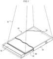
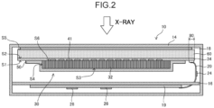
- the support plate 16 is fixed to the case 14, and supports a circuit board 19 (see Fig. 2 ) to which is mounted an integrated circuit chip for performing signal processing and the like.
- the control unit 12 is arranged at an end portion inside the case 14.
- the control unit 12 is configured including a battery (not illustrated in the drawings) and a controller 29 (see Fig. 3 ).
- terbium-doped gadolinium oxysulfide (Gd 2 O 2 S:Tb) may be employed as the material of the scintillator 32.
- Each of the respective photoelectric conversion elements 36 (see Fig. 3 ) configuring the plural pixels 41 generates an electrical charge based on the light emitted from the scintillator 32.
- the substrate 34 is arranged at the radiation-incident side and the radiographic imaging device 10 employs an irradiation side sampling (ISS) imaging method.
- ISS irradiation side sampling
- Adopting the irradiation side sampling method enables the distance been positions of intense light emission in the scintillator 32 and the pixels 41 to be shortened compared to when employing a penetration side sampling (PSS) method, in which the scintillator 32 is arranged at the radiation-incident side. This thereby enables radiographic images to be obtained with higher resolution.
- the radiographic imaging device 10 may employ penetration side sampling.
- the support plate 16 is arranged at the opposite side of the scintillator 32 to the radiation-incident side. A gap is provided between the support plate 16 and the scintillator 32.
- the support plate 16 is fixed to side portions of the case 14.
- the circuit board 19 is provided on the surface of the support plate 16 on the opposite side to the scintillator 32.
- the circuit board 19 is mounted with a signal processor 26 for generating image data, an image memory 28 for storing the image data generated by the signal processor 26, and the like.
- the circuit board 19 and the substrate 34 are electrically connected together through a flexible cable 20 printed on a flexible printed circuit (FPC) and a tape carrier package (TCP) or a chip-on-film (COF).
- Charging amplifiers 24 for converting electrical charge read from the pixels 41 into electrical signals are mounted on the cable 20.
- a gate line driver 22 (see Fig. 3 ) that is electrically connected to the circuit board 19 and the substrate 34 is mounted to a separate flexible printed circuit not illustrated in Fig. 2 .
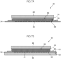
- the bending suppression member 60 is stacked on the second surface S2 side of the substrate 34 on the opposite side to the first surface S1.
- the bending suppression member 60 has the role of imparting the substrate 34 with the necessary rigidity for the substrate 34 to support the scintillator 32. Namely, providing the bending suppression member 60 suppresses the substrate 34 from bending due to the weight of the scintillator 32 compared to cases in which the bending suppression member 60 is omitted.
- the bending suppression member 60 extends over a wider range than an extension range of the scintillator 32.
- the substrate 34 has a tendency to bend even in the connection region 80 where the flexible cable 20 is connected, providing the bending suppression member 60 in the region covering at least a portion of the connection region 80 enables bending in the connection region 80 of the substrate 34 to be suppressed.
- Fig. 3 is a diagram illustrating an example of an electrical configuration of the radiographic imaging device 10.
- Plural pixels 41 are arranged in a matrix formation on the first surface S1 of the substrate 34.
- Each of the pixels 41 includes a photoelectric conversion element 36 and a thin film transistor (TFT) 42.
- the photoelectric conversion element 36 generates electrical charge according to the light emitted from the scintillator 32.
- the TFT 42 serves as a switching element that is switched to an ON state in order to read the electrical charge generated in the photoelectric conversion element 36.
- the photoelectric conversion element 36 may, for example, be a photodiode configured from amorphous silicon.
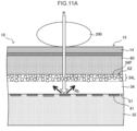
- the scintillator 32 absorbs the radiation and emits visible light.
- the photoelectric conversion elements 36 configuring the respective pixels 41 convert the light emitted from the scintillator 32 into electrical charge.
- the electrical charge generated by each of the photoelectric conversion elements 36 is accumulated in the corresponding pixel 41.
- the amount of electrical charge generated by the photoelectric conversion element 36 is reflected in a pixel value of the corresponding pixel 41.
- the gate line driver 22 supplies a gate signal to the TFTs 42 through gate lines 43 based on a control signal supplied from the controller 29.
- the TFTs 42 are switched to the ON state by the gate signal in row units. Due to the TFTs 42 being switched to the ON state, the electrical charge accumulated in each of the pixels 41 is read through the corresponding signal line 44, and is supplied to the corresponding charging amplifier 24.
- the charging amplifiers 24 generate electrical signals based on the electrical charges read from the signal lines 44 and supply the generated electrical signals to the signal processor 26.
- the signal processor 26 is equipped with plural sample-and-hold circuits, a multiplexer, and an analogue-to-digital converter (none of which are illustrated in the drawings).
- the plural sample-and-hold circuits are provided so as to correspond to each of the respective plural signal lines 44.
- the electrical signals supplied from the charging amplifiers 24 are held in the sample-and-hold circuits.
- the electrical signals held in the individual sample-and-hold circuits are each input to the analogue-to-digital converter through the multiplexer to be converted into digital signals.
- the signal processor 26 generates, as image data, data in which the digital signals generated by the analogue-to-digital converter are associated with information about the positions of the respective pixels 41, and supplies this image data to the image memory 28.
- the image memory 28 stores the image data generated by the signal processor 26.
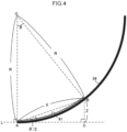
- the length of the long side is preferably applied as the size of the pixel 41 (photoelectric conversion element 36).
- Z in Fig. 4 is a deformation amount of the pixel 41 due to bending of the substrate 34.
- the deformation amount Z corresponds to a distance (length of a line segment BC) between a tangent L to one end portion of the pixel 41 (point A) and the other end portion of the pixel 41 (point B).
- ⁇ in Fig. 4 corresponds to a central angle of a sector including an arc AB.
- Equation (2) can be derived therefrom since ⁇ BAC is ⁇ /2.
- the maximum value of the deformation amount Z at which the pixel 41 is not damaged (also referred below to as the critical deformation amount) is denoted Z L .
- the risk of damaging the pixel 41 can be reduced by limiting the range of the radius of curvature R when bending the substrate 34 to the range given in Equation (5) below.
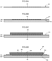
- Fig. 6A to Fig. 6D are cross-sections illustrating an example of a method of manufacturing the radiation detector 30.
- the plural pixels 41 are formed on the first surface S1 of the substrate 34 ( Fig. 6A ). Note that formation of the pixels 41 may be performed in a state in which the substrate 34 is supported by a support body (not illustrated in the drawings) to support the substrate 34.
- the bending suppression member 60 is stuck to the second surface S2 of the substrate 34 on the opposite side to the first surface S1 of the substrate 34 ( Fig. 6B ).
- the bending suppression member 60 has a rigidity such that the radius of curvature R of bending that occurs in the substrate 34 due to the weight of the scintillator 32 satisfies Equation (5).
- the rigidity of the bending suppression member 60 is set higher the greater the size X of the pixels 41.
- the reflective film 50 is then formed so as to cover the surface S3 of scintillator 32 on the opposite side to the surface S6 contacting the substrate 34, and to cover the surface S4 that intersects with the surface S3 ( Fig. 6D ).
- Al 2 O 3 may, for example, be employed as the material of the reflective film 50.
- the reflective film 50 is formed so as to cover the substrate 34 at portions in the vicinity of the scintillator 32.
- the rigidity of the bending suppression member 60 is set such that the radius of curvature R of bending that occurs in the substrate 34 due to the weight of the scintillator 32 satisfies Equation (5).
- the radius of curvature R of bending that occurs in the substrate 34 due to the weight of the scintillator 32 is limited to the range of Equation (5). This thereby enables the risk of the pixels 41 being damaged when, for example, the substrate 34 is handled during processes to manufacture the radiation detector 30 to be reduced, even when bending occurs in the substrate 34 due to the weight of the scintillator 32, compared to cases in which the technology disclosed herein is not applied.
- the bending suppression member 60 is stacked on both the second surface S2 side of the substrate 34 and on the surface S3 side of the scintillator 32 that is the opposite side to the surface S6 in contact with the substrate 34. Stacking the bending suppression member 60 on at least one side from out of the second surface S2 side of the substrate 34 or the surface S3 side of the scintillator 32 that is the opposite side to the surface S6 in contact with the substrate 34 enhances the bending suppression effect exhibited by the bending suppression member 60. Moreover, as illustrated in Fig.
- Fig. 8A is a cross-section illustrating an example of a configuration of a radiation detector 30A according to a second exemplary embodiment of technology disclosed herein.
- the radiation detector 30A differs from the radiation detector 30 according to the first exemplary embodiment in the point that reinforcement members 70 are further included in order to reinforce the bending suppression effect of the bending suppression member 60.
- the reinforcement members 70 are provided in regions straddling the end portions 32E of the scintillator 32 in order to reinforce the bending suppression effect of the bending suppression member 60. This enables the bending of the portions of the substrate 34 corresponding to the end portions 32E of the scintillator 32 to be suppressed compared to cases in which the reinforcement members 70 are not provided. Thus the risk of the pixels 41 being damaged can be reduced compared to cases in which the reinforcement members 70 are not provided.
- the reflective film 50 covers the entire front surface of the adhesion layer 51.
- the reflective film 50 has a function of reflecting the light converted in the scintillator 32.
- the reflective film 50 is preferably configured from an organic material. Examples of materials that may be employed for the reflective film 50 include white polyethylene terephthalate (PET), TiO 2 , Al 2 O 3 , foamed white PET, polyester-based high reflectivity sheets, specular reflective aluminum, and the like.
- white PET is PET to which a white pigment, such as TiO 2 , barium sulfate, or the like, has been added.
- polyester-based high reflectivity sheets are sheets (films) having a multi-layer structure of plural superimposed thin polyester sheets.
- Foamed white PET is white PET having a porous surface.
- the thickness of the reflective film 50 is preferably from 10 ⁇ m to 40 ⁇ m.
- the bonding layer 52 covers the entire front surface of the reflective film 50.
- the end portion of the bonding layer 52 also extends as far as the front surface of the substrate 34. Namely, the bonding layer 52 is bonded to the substrate 34 at these end portions.
- the bonding layer 52 has a function to fix the reflective film 50 and the protective layer 53 to the scintillator 32.
- the same materials as may be employed in the adhesion layer 51 may be employed as the material of the bonding layer 52.
- the bonding strength of the bonding layer 52 is preferably greater than the bonding strength of the adhesion layer 51.
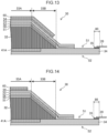
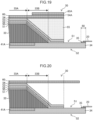
- the bending suppression member 60 may be configured without providing an angled portion to follow the slope of the outer peripheral portions of the scintillator 32.
- the bending suppression member 60 is bonded to the protective layer 53 through the bonding layer 54 in the region corresponding to the central portion 33A of the scintillator 32.
- a space corresponding to the slope of the peripheral edge portion 33B of the scintillator 32 is formed between the scintillator 32 (the protective layer 53) and the bending suppression member 60 in the region corresponding to the peripheral edge portion 33B of the scintillator 32.
- the cable 20 is connected to terminals 35 provided in the connection region 80 at the outer peripheral portion of the substrate 34.
- the substrate 34 is connected to a control board (see Fig. 45 ) through the cable 20.
- a control board see Fig. 45
- the cable 20 might detach from the substrate 34 or positional misalignment might arise were bending of the substrate 34 to occur. In such cases it would be necessary to perform a task to reconnect the cable 20 and the substrate 34.
- This task to reconnect the cable 20 and the substrate 34 is called re-work.
- re-work As illustrated in Fig. 13 to Fig. 15 , by arranging the end portion of the bending suppression member 60 at the inside of the end portion of the scintillator 32, re-work can be performed more easily than in cases in which the bending suppression member 60 extends to the vicinity of the connection region 80.
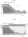
- a filler 55 is provided in the space formed between the scintillator 32 (the protective layer 53) and the bending suppression member 60 at the region corresponding to the peripheral edge portion 33B of the scintillator 32 and also at the region further to the outside thereof.
- the material of the filler 55 is not particularly limited, and examples of materials that may be employed therefor include, for example, resins.
- the bonding layer 54 is provided in the entire region between the bending suppression member 60 and the filler 55 in order to fix the bending suppression member 60 to the filler 55.
- the method of forming the filler 55 is not particularly limited.
- a flowable filler 55 may be poured into be the space formed between the scintillator 32 (the protective layer 53) and the bending suppression member 60, and the filler 55 then cured.
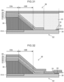
- the outer peripheral portion of the bending suppression member 60 is angled so as to follow the slope of the peripheral edge portion 33B of the scintillator 32, and so as also to cover the portions of the bonding layer 52 and the protective layer 53 that cover the substrate 34. Moreover, the end portion of the bending suppression member 60 and the end portions of the bonding layer 52 and the protective layer 53 are aligned with each other. Note that there is no need for the position of the end portion of the bending suppression member 60 to align exactly with the position of the end portions of the bonding layer 52 and the protective layer 53.
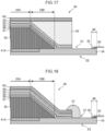
- an additional and separate bending suppression member 60A is stacked on a front surface of the bending suppression member 60 at a region corresponding to the end portion of the scintillator 32, with a bonding layer 54A interposed therebetween. More specifically, the bending suppression member 60A is provided in a region straddling the end portion (outer edge, edge) of the scintillator 32.
- the bending suppression member 60A may be configured from the same materials as the bending suppression member 60. As illustrated in Fig. 9 , the amount of bending of the substrate 34 is comparatively large at the end portions of the scintillator 32.
- the space formed between the scintillator 32 (the protective layer 53) and the bending suppression member 60, and between the substrate 34 and the bending suppression member 60, is filled by the filler 55.
- the connection portions between the cable 20 and the terminals 35 are covered by the filler 55.
- the outer peripheral portion of the bending suppression member 60 is angled so as to follow the slope of the peripheral edge portion 33B of the scintillator 32.
- the outer peripheral portion of the bending suppression member 60 also covers a portion where the bonding layer 52 and the protective layer 53 cover the substrate 34, a portion of the substrate at the outside thereof, and the connection portion between the cable 20 and the terminals 35.
- the portions of the bending suppression member 60 extending over the substrate 34 and over the cable 20 are respectively bonded to the substrate 34 and the cable 20 through the bonding layer 54.
- the connection portions between the cable 20 and the terminals 35 are covered by the bending suppression member 60, enabling detachment of the cable 20 to be suppressed.
- an additional and separate bending suppression member 60A is stacked on a front surface of the bending suppression member 60 at a region corresponding to the end portion of the scintillator 32, with a bonding layer 54A interposed therebetween. More specifically, the bending suppression member 60A is provided in a region straddling the end portion (outer edge, edge) of the scintillator 32.
- the bending suppression member 60A may be configured from the same materials as the bending suppression member 60. As illustrated in Fig.
- the scintillator 32 having a structure fixed to the substrate 34 by both the bending suppression member 60 and the filler 55, the scintillator 32 and the substrate 34 can be suppressed from detaching from one another. Moreover, since the connection portions between the cable 20 and the terminals 35 are covered by the filler 55, detachment of the cable 20 can be suppressed.
- the outer peripheral portion of the bending suppression member 60 is angled so as to follow the slope of the peripheral edge portion 33B of the scintillator 32.
- the outer peripheral portion of the bending suppression member 60 also covers the portion where the bonding layer 52 and the protective layer 53 cover the substrate 34, the portion on the substrate at the outside thereof, and the connection portion between the cable 20 and the terminals 35.
- the portions of the bending suppression member 60 extending over the substrate 34 and over the cable 20 are respectively bonded to the substrate 34 and the cable 20 through the bonding layer 54.
- connection portions between the cable 20 and the terminals 35 are covered by the bending suppression member 60, enabling bending of the substrate 34 at these portions to be suppressed.
- the amount of bending of the substrate 34 is comparatively large at the end portions of the scintillator 32.
- Forming a multi-layer structure using the bending suppression members 60 and 60A at the region corresponding to the end portion of the scintillator 32 enables the effect of suppressing bending of the substrate 34 to be enhanced at the end portion of the scintillator 32.
- the flexible substrate 34 is stuck to a support body, such as a glass substrate or the like, and then after stacking the scintillator 32 onto the substrate 34, the support body is detached from the substrate 34.
- a support body such as a glass substrate or the like
- the support body is detached from the substrate 34.
- bending occurs in the flexible substrate 34, and there is a concern that the pixels 41 formed on the substrate 34 might be damaged thereby.
- the bending suppression member 60 on the scintillator 32 as in the embodiments illustrated in the examples of Fig. 13 to Fig. 33 prior to detaching the support body from the substrate 34, the bending of the substrate 34 that occurs when the support body is being detached from the substrate 34 can be suppressed, enabling the risk of damage of the pixels 41 to be reduced.
- the bending suppression member 60A is preferably provided only on the outer peripheral portion of the substrate 34 in order to keep the surface area of the overlapping portion between the bending suppression member 60A and the pixel region 41A as small as possible.
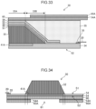
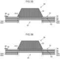
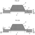
- the bending suppression member 60A may have a ring shape including an opening 61 at a portion corresponding to the pixel region 41A, as illustrated in Fig. 34 to Fig. 39 .
- the bending suppression member 60A is provided in a region straddling the end portion (outer edge, edge) of the scintillator 32. As illustrated in Fig. 9 , the amount of bending of the substrate 34 is comparatively large at the end portions of the scintillator 32. Forming a multi-layer structure using the bending suppression members 60 and 60A at the region corresponding to the end portion of the scintillator 32 enables the effect of suppressing bending of the substrate 34 to be enhanced at the end portion of the scintillator 32.
- the bending suppression member 60A straddles the end portion (outer edge, edge) of the scintillator 32 but does not overlap with the pixel region 41A (namely, an embodiment in which an edge of the opening 61 of the bending suppression member 60A is disposed at the outside of the pixel region 41A).
- the position of the edge of the opening 61 of the bending suppression member 60A is substantially aligned with the position of the end portion of the pixel region 41A.
- the edge of the opening 61 of the bending suppression member 60A is disposed between the end portion of the pixel region 41A and the end portion of the scintillator 32.
- the position of the edge of the opening 61 of the bending suppression member 60A may be disposed so as to be substantially aligned with the position of the end portion of the scintillator 32 as illustrated in Fig. 37 , or may be disposed so as to be further outside than the end portion of the scintillator 32 as illustrated in Fig. 38 .
- the bending suppression member 60A straddles the end portion (outer edge, edge) of the scintillator 32, and so there might be a concern regarding a lessening of the effect of suppressing bending of the substrate 34 at the end portion of the scintillator 32.
- the surface area of the bending suppression member 60 is larger than the surface area of the substrate 34, and the end portion of the bending suppression member 60 is disposed further outside than the end portion of the substrate 34. Adopting such an embodiment enables the radiation detector 30 to be fixed to the inside of the case 14 by screwing a portion of the bending suppression member 60 that juts out from the substrate 34 to the case 14, or the like.
- Fig. 34 to Fig. 39 examples are illustrated in which the position of the outside end portion of the bending suppression member 60A is substantially aligned with the position of the end portion of the substrate 34, there is no limitation to such embodiments.
- the outside end portion of the bending suppression member 60A may be disposed further to the outside or inside than the end portion of the substrate 34.
- a multi-layer structure is formed using the bending suppression members 60 and 60A at the second surface S2 side of the substrate 34
- the bending suppression member 60 may be provided alone at the second surface S2 side of the substrate 34 in order to reinforce the outer peripheral portion of the substrate 34.
- the case 14 preferably includes a sloping portion 14A at a portion where these two regions are connected together.
- a base 37 having substantially the same size as that of the substrate 34 of the radiation detector 30 is provided at a position overlapping with the substrate 34 within the internal space of the case 14, and the control board 81 and the power source 82 are provided on the base 37. Adopting such a configuration enables the size of the radiographic imaging device 10 in plan view to be decreased in comparison to cases in which the radiation detector 30, the control board 81, and the power source 82 are arranged next to each other along the lateral direction in the drawings.
Landscapes
- Health & Medical Sciences (AREA)
- Life Sciences & Earth Sciences (AREA)
- Physics & Mathematics (AREA)
- High Energy & Nuclear Physics (AREA)
- Molecular Biology (AREA)
- General Physics & Mathematics (AREA)
- Spectroscopy & Molecular Physics (AREA)
- Medical Informatics (AREA)
- Engineering & Computer Science (AREA)
- Crystallography & Structural Chemistry (AREA)
- Chemical & Material Sciences (AREA)
- Nuclear Medicine, Radiotherapy & Molecular Imaging (AREA)
- Surgery (AREA)
- Optics & Photonics (AREA)
- Pathology (AREA)
- Radiology & Medical Imaging (AREA)
- Biomedical Technology (AREA)
- Heart & Thoracic Surgery (AREA)
- Biophysics (AREA)
- Animal Behavior & Ethology (AREA)
- General Health & Medical Sciences (AREA)
- Public Health (AREA)
- Veterinary Medicine (AREA)
- Measurement Of Radiation (AREA)
- Apparatus For Radiation Diagnosis (AREA)
Claims (12)
- Détecteur de radiation comprenant :un substrat flexible (34) ;une pluralité de pixels (41) disposés sur le substrat (34) et incluant chacun un élément de conversion photoélectrique (36) ;un scintillateur (32) empilé sur un premier côté de surface du substrat (34) ; etun élément de suppression de flexion (60) configuré pour supprimer la flexion du substrat (34), l'élément de suppression de flexion (60) étant empilé à la fois sur un deuxième côté de surface du substrat (34) et sur le côté correspondant à la surface du scintillateur (32) du côté opposé à la surface du scintillateur (32) en contact avec le substrat (34),caractérisé en ce que l'élément de suppression de flexion (60) est configuré de manière à inclure au moins l'un des matériaux acrylique, polycarbonate ou polyéthylène téréphtalate.
- Détecteur de radiation selon la revendication 1, dans lequel l'élément de suppression de flexion (60) a une rigidité supérieure à celle du substrat (34).
- Détecteur de radiation selon l'une quelconque des revendications 1 à 2, dans lequel l'élément de suppression de flexion (60) s'étend de manière à couvrir une plage plus large qu'une plage d'extension du scintillateur (32).
- Détecteur de radiation selon l'une quelconque des revendications 1 à 3, dans lequel :le substrat (34) inclut une région de connexion (80) pour une connexion de câblage flexible ; etl'élément de suppression de flexion (60) est prévu dans une région couvrant au moins une portion de la région de connexion (80) et couvrant également le scintillateur (32).
- Détecteur de radiation selon l'une quelconque des revendications 1 à 4, dans lequel l'élément de suppression de flexion (60) a un module d'élasticité en flexion de 1000 MPa à 3500 MPa.
- Détecteur de radiation selon l'une quelconque des revendications 1 à 5, dans lequel un rapport d'un coefficient de dilatation thermique de l'élément de suppression de flexion (60) sur un coefficient de dilatation thermique du scintillateur (32) est compris entre 0,5 et 2.
- Détecteur de radiation selon l'une quelconque des revendications 1 à 6, dans lequel un coefficient de dilatation thermique de l'élément de suppression de flexion (60) est compris entre 30 ppm/K et 80 ppm/K.
- Détecteur de radiation selon l'une quelconque des revendications 1 à 7, comprenant en outre des membres de renforcement (70) prévus dans une région enjambant les limites entre la région où le scintillateur (32) est présent et les régions où le scintillateur (32) n'est pas présent et sur un côté opposé à un côté du substrat (34) sur lequel le scintillateur (32) est prévu de manière à renforcer un effet de suppression de flexion de l'élément de suppression de flexion (60).
- Détecteur de radiation selon l'une quelconque des revendications 1 à 8, comprenant en outre une couche amortissante (90) qui est prévue entre le substrat (34) et le scintillateur (32) et qui a un coefficient de dilatation thermique compris entre le coefficient de dilatation thermique du substrat (34) et le coefficient de dilatation thermique du scintillateur (32).
- Un dispositif d'imagerie radiographique comprenant :le détecteur de radiation (30) selon l'une quelconque des revendications 1 à 9 ;une section de lecture (22) configurée pour effectuer une lecture de charge électrique accumulée dans les pixels (41) ; etune section de génération (26) configurée pour générer des données d'image sur la base de la charge électrique lue à partir des pixels (41).
- Le dispositif d'imagerie radiographique selon la revendication 10, comprenant en outre :un boîtier (14) qui loge le détecteur de radiation (30) et qui inclut une face d'incidence de radiation (15) sur laquelle la radiation est incidente ; etparmi le substrat (34) et le scintillateur (32), le substrat (34) est disposé sur un côté correspondant à la face d'incidence de radiation (15).
- Un procédé de fabrication d'un détecteur de radiation comprenant :former une pluralité de pixels (41) sur un substrat flexible (34) d'une manière que chaque pixel (41) inclut un élément de conversion photoélectrique (36) ;former un scintillateur (32) sur un premier côté de surface du substrat (34) ; etdisposer un élément de suppression de flexion (60) configuré pour supprimer la flexion du substrat (34) à la fois sur un deuxième côté de surface du substrat (34) et sur le côté correspondant à la surface du scintillateur (32) sur le côté opposé à la surface du scintillateur (32) en contact avec le substrat (34) ;l'élément de suppression de flexion (60) étant défini avec une rigidité d'autant plus élevée que la taille d'un pixel est grande,caractérisé en ce que l'élément de suppression de flexion (60) est configuré pour inclure au moins l'un des matériaux acrylique, polycarbonate ou polyéthylène téréphtalate.
Applications Claiming Priority (4)
| Application Number | Priority Date | Filing Date | Title |
|---|---|---|---|
| JP2018051691 | 2018-03-19 | ||
| JP2018219697 | 2018-11-22 | ||
| JP2019022081 | 2019-02-08 | ||
| PCT/JP2019/009954 WO2019181640A1 (fr) | 2018-03-19 | 2019-03-12 | Détecteur de rayonnement, dispositif de photographie radiographique et procédé de production de détecteur de rayonnement |
Publications (3)
| Publication Number | Publication Date |
|---|---|
| EP3770639A1 EP3770639A1 (fr) | 2021-01-27 |
| EP3770639A4 EP3770639A4 (fr) | 2021-04-14 |
| EP3770639B1 true EP3770639B1 (fr) | 2025-04-09 |
Family
ID=67987608
Family Applications (1)
| Application Number | Title | Priority Date | Filing Date |
|---|---|---|---|
| EP19770801.9A Active EP3770639B1 (fr) | 2018-03-19 | 2019-03-12 | Détecteur de rayonnement, dispositif de photographie radiographique et procédé de production de détecteur de rayonnement |
Country Status (6)
| Country | Link |
|---|---|
| US (1) | US11609347B2 (fr) |
| EP (1) | EP3770639B1 (fr) |
| JP (2) | JP7314118B2 (fr) |
| CN (2) | CN110286401B (fr) |
| TW (1) | TWI821255B (fr) |
| WO (1) | WO2019181640A1 (fr) |
Families Citing this family (11)
| Publication number | Priority date | Publication date | Assignee | Title |
|---|---|---|---|---|
| JP7314118B2 (ja) * | 2018-03-19 | 2023-07-25 | 富士フイルム株式会社 | 放射線検出器、放射線画像撮影装置及び放射線検出器の製造方法 |
| WO2021166779A1 (fr) * | 2020-02-20 | 2021-08-26 | 富士フイルム株式会社 | Détecteur de rayonnement, dispositif de radiographie et procédé de production de détecteur de rayonnement |
| TWI734489B (zh) * | 2020-05-22 | 2021-07-21 | 睿生光電股份有限公司 | X射線裝置及其製造方法 |
| WO2022071549A1 (fr) | 2020-10-01 | 2022-04-07 | 大日本印刷株式会社 | Dispositif de détection |
| JP7587980B2 (ja) * | 2020-12-23 | 2024-11-21 | 浜松ホトニクス株式会社 | 放射線検出器、放射線検出器の製造方法、及びシンチレータパネルユニット |
| JP2022129240A (ja) * | 2021-02-24 | 2022-09-05 | ソニーセミコンダクタソリューションズ株式会社 | 固体撮像装置及びその製造方法 |
| KR102373241B1 (ko) * | 2021-06-15 | 2022-03-15 | 주식회사 디알텍 | 방사선 디텍터 및 이를 포함하는 방사선 검사장치 |
| JP7612529B2 (ja) * | 2021-06-21 | 2025-01-14 | 富士フイルム株式会社 | 放射線画像撮影装置 |
| JP2024064190A (ja) * | 2022-10-27 | 2024-05-14 | キヤノン株式会社 | 放射線撮像装置および放射線撮影システム |
| EP4419949B1 (fr) * | 2022-12-30 | 2026-01-21 | Shanghai United Imaging Healthcare Co., Ltd. | Détecteurs de comptage de photons pour la détection de rayons de rayonnement |
| CN116735631B (zh) * | 2023-08-09 | 2024-02-23 | 同源微(北京)半导体技术有限公司 | 一种x射线成像检测单元、模块和装置 |
Family Cites Families (19)
| Publication number | Priority date | Publication date | Assignee | Title |
|---|---|---|---|---|
| US6414315B1 (en) * | 1999-10-04 | 2002-07-02 | General Electric Company | Radiation imaging with continuous polymer layer for scintillator |
| JP3848288B2 (ja) | 2003-04-25 | 2006-11-22 | キヤノン株式会社 | 放射線画像撮影装置 |
| JP2007071836A (ja) * | 2005-09-09 | 2007-03-22 | Canon Inc | 放射線検出装置及び放射線撮像システム |
| JP2011128172A (ja) * | 2008-04-10 | 2011-06-30 | Konica Minolta Medical & Graphic Inc | 可搬型放射線固体検出器 |
| US8106363B2 (en) | 2008-04-17 | 2012-01-31 | Carestream Health, Inc. | Digital radiography panel with pressure-sensitive adhesive for optical coupling between scintillator screen and detector and method of manufacture |
| JP2011247826A (ja) * | 2010-05-28 | 2011-12-08 | Fujifilm Corp | 放射線検出パネル及びその製造方法 |
| JP2012128091A (ja) * | 2010-12-14 | 2012-07-05 | Fujifilm Corp | 放射線画像撮影装置 |
| JP5557773B2 (ja) | 2011-02-24 | 2014-07-23 | 富士フイルム株式会社 | 放射線画像検出装置及び放射線撮影用カセッテ並びに放射線撮影装置 |
| JP2013217769A (ja) | 2012-04-09 | 2013-10-24 | Canon Inc | 放射線検出装置 |
| JP2014032170A (ja) | 2012-07-11 | 2014-02-20 | Konica Minolta Inc | 放射線検出パネルおよび放射線画像検出器 |
| JP5815483B2 (ja) * | 2012-07-27 | 2015-11-17 | 富士フイルム株式会社 | 放射線画像撮影装置 |
| JP2014081363A (ja) * | 2012-09-27 | 2014-05-08 | Fujifilm Corp | 放射線画像検出装置 |
| JP6310216B2 (ja) * | 2013-09-06 | 2018-04-11 | キヤノン株式会社 | 放射線検出装置及びその製造方法並びに放射線検出システム |
| US9689997B2 (en) | 2014-09-04 | 2017-06-27 | General Electric Company | Systems and methods for modular imaging detectors |
| CN106662686B (zh) | 2015-07-28 | 2020-06-23 | Jsr株式会社 | 光学滤波器、环境光传感器及电子设备 |
| KR102547798B1 (ko) * | 2015-12-08 | 2023-06-26 | 삼성전자주식회사 | 방사선 검출기 및 이를 채용한 방사선 촬영 장치 |
| JP2018051691A (ja) | 2016-09-29 | 2018-04-05 | 株式会社リケン | リングケース |
| JP2019022081A (ja) | 2017-07-18 | 2019-02-07 | シャープ株式会社 | 端末装置、基地局装置、および、通信方法 |
| JP7314118B2 (ja) * | 2018-03-19 | 2023-07-25 | 富士フイルム株式会社 | 放射線検出器、放射線画像撮影装置及び放射線検出器の製造方法 |
-
2019
- 2019-03-12 JP JP2020508241A patent/JP7314118B2/ja active Active
- 2019-03-12 EP EP19770801.9A patent/EP3770639B1/fr active Active
- 2019-03-12 WO PCT/JP2019/009954 patent/WO2019181640A1/fr not_active Ceased
- 2019-03-15 TW TW108108937A patent/TWI821255B/zh active
- 2019-03-18 CN CN201910206423.1A patent/CN110286401B/zh active Active
- 2019-03-18 CN CN201920344792.2U patent/CN210005700U/zh active Active
-
2020
- 2020-09-11 US US17/018,225 patent/US11609347B2/en active Active
-
2022
- 2022-04-04 JP JP2022062629A patent/JP7376636B2/ja active Active
Also Published As
| Publication number | Publication date |
|---|---|
| JP7376636B2 (ja) | 2023-11-08 |
| JP7314118B2 (ja) | 2023-07-25 |
| JPWO2019181640A1 (ja) | 2021-02-18 |
| WO2019181640A1 (fr) | 2019-09-26 |
| EP3770639A4 (fr) | 2021-04-14 |
| US20200408935A1 (en) | 2020-12-31 |
| CN110286401A (zh) | 2019-09-27 |
| JP2022101584A (ja) | 2022-07-06 |
| TWI821255B (zh) | 2023-11-11 |
| TW201940898A (zh) | 2019-10-16 |
| EP3770639A1 (fr) | 2021-01-27 |
| CN210005700U (zh) | 2020-01-31 |
| US11609347B2 (en) | 2023-03-21 |
| CN110286401B (zh) | 2025-08-15 |
Similar Documents
| Publication | Publication Date | Title |
|---|---|---|
| EP3770639B1 (fr) | Détecteur de rayonnement, dispositif de photographie radiographique et procédé de production de détecteur de rayonnement | |
| US11221421B2 (en) | Radiation detector, radiographic imaging device, and radiation detector manufacturing method | |
| US11624716B2 (en) | Radiation detector and radiographic imaging device | |
| US11630221B2 (en) | Radiation detector, radiographic imaging device, and manufacturing method | |
| US11262461B2 (en) | Radiation detector and radiographic imaging device | |
| US11786194B2 (en) | Radiation detector comprising a reinforcement substrate, radiographic imaging device, and manufacturing method | |
| US11428827B2 (en) | Radiation detector, radiographic imaging apparatus, and manufacturing method | |
| US11417440B2 (en) | Radiographic imaging apparatus and method of manufacturing radiographic imaging apparatus | |
| US11877875B2 (en) | Radiation detector, radiographic imaging apparatus, and method of manufacturing radiation detector | |
| US11802981B2 (en) | Method of manufacturing radiation detector and radiographic imaging apparatus | |
| US11766227B2 (en) | Radiation detector, radiographic imaging apparatus, and method of manufacturing radiation detector | |
| US20220381930A1 (en) | Radiation detector, radiographic imaging apparatus, and method of manufacturing radiation detector |
Legal Events
| Date | Code | Title | Description |
|---|---|---|---|
| STAA | Information on the status of an ep patent application or granted ep patent |
Free format text: STATUS: THE INTERNATIONAL PUBLICATION HAS BEEN MADE |
|
| PUAI | Public reference made under article 153(3) epc to a published international application that has entered the european phase |
Free format text: ORIGINAL CODE: 0009012 |
|
| STAA | Information on the status of an ep patent application or granted ep patent |
Free format text: STATUS: REQUEST FOR EXAMINATION WAS MADE |
|
| 17P | Request for examination filed |
Effective date: 20200921 |
|
| AK | Designated contracting states |
Kind code of ref document: A1 Designated state(s): AL AT BE BG CH CY CZ DE DK EE ES FI FR GB GR HR HU IE IS IT LI LT LU LV MC MK MT NL NO PL PT RO RS SE SI SK SM TR |
|
| AX | Request for extension of the european patent |
Extension state: BA ME |
|
| A4 | Supplementary search report drawn up and despatched |
Effective date: 20210316 |
|
| RAP3 | Party data changed (applicant data changed or rights of an application transferred) |
Owner name: FUJIFILM CORPORATION |
|
| RIC1 | Information provided on ipc code assigned before grant |
Ipc: G01T 1/20 20060101AFI20210310BHEP |
|
| DAV | Request for validation of the european patent (deleted) | ||
| DAX | Request for extension of the european patent (deleted) | ||
| RIN1 | Information on inventor provided before grant (corrected) |
Inventor name: AKAMATSU, KEIICHI Inventor name: NAKATSUGAWA, HARUYASU Inventor name: KATO, MUNETAKA Inventor name: IWAKIRI, NAOTO |
|
| STAA | Information on the status of an ep patent application or granted ep patent |
Free format text: STATUS: EXAMINATION IS IN PROGRESS |
|
| 17Q | First examination report despatched |
Effective date: 20221116 |
|
| GRAP | Despatch of communication of intention to grant a patent |
Free format text: ORIGINAL CODE: EPIDOSNIGR1 |
|
| STAA | Information on the status of an ep patent application or granted ep patent |
Free format text: STATUS: GRANT OF PATENT IS INTENDED |
|
| INTG | Intention to grant announced |
Effective date: 20240715 |
|
| GRAJ | Information related to disapproval of communication of intention to grant by the applicant or resumption of examination proceedings by the epo deleted |
Free format text: ORIGINAL CODE: EPIDOSDIGR1 |
|
| STAA | Information on the status of an ep patent application or granted ep patent |
Free format text: STATUS: EXAMINATION IS IN PROGRESS |
|
| GRAP | Despatch of communication of intention to grant a patent |
Free format text: ORIGINAL CODE: EPIDOSNIGR1 |
|
| STAA | Information on the status of an ep patent application or granted ep patent |
Free format text: STATUS: GRANT OF PATENT IS INTENDED |
|
| INTC | Intention to grant announced (deleted) | ||
| INTG | Intention to grant announced |
Effective date: 20241108 |
|
| GRAS | Grant fee paid |
Free format text: ORIGINAL CODE: EPIDOSNIGR3 |
|
| GRAA | (expected) grant |
Free format text: ORIGINAL CODE: 0009210 |
|
| STAA | Information on the status of an ep patent application or granted ep patent |
Free format text: STATUS: THE PATENT HAS BEEN GRANTED |
|
| P01 | Opt-out of the competence of the unified patent court (upc) registered |
Free format text: CASE NUMBER: APP_9440/2025 Effective date: 20250225 |
|
| AK | Designated contracting states |
Kind code of ref document: B1 Designated state(s): AL AT BE BG CH CY CZ DE DK EE ES FI FR GB GR HR HU IE IS IT LI LT LU LV MC MK MT NL NO PL PT RO RS SE SI SK SM TR |
|
| REG | Reference to a national code |
Ref country code: GB Ref legal event code: FG4D |
|
| REG | Reference to a national code |
Ref country code: CH Ref legal event code: EP |
|
| REG | Reference to a national code |
Ref country code: DE Ref legal event code: R096 Ref document number: 602019068440 Country of ref document: DE |
|
| REG | Reference to a national code |
Ref country code: IE Ref legal event code: FG4D |
|
| REG | Reference to a national code |
Ref country code: NL Ref legal event code: FP |
|
| REG | Reference to a national code |
Ref country code: AT Ref legal event code: MK05 Ref document number: 1784002 Country of ref document: AT Kind code of ref document: T Effective date: 20250409 |
|
| PG25 | Lapsed in a contracting state [announced via postgrant information from national office to epo] |
Ref country code: PT Free format text: LAPSE BECAUSE OF FAILURE TO SUBMIT A TRANSLATION OF THE DESCRIPTION OR TO PAY THE FEE WITHIN THE PRESCRIBED TIME-LIMIT Effective date: 20250811 Ref country code: FI Free format text: LAPSE BECAUSE OF FAILURE TO SUBMIT A TRANSLATION OF THE DESCRIPTION OR TO PAY THE FEE WITHIN THE PRESCRIBED TIME-LIMIT Effective date: 20250409 Ref country code: ES Free format text: LAPSE BECAUSE OF FAILURE TO SUBMIT A TRANSLATION OF THE DESCRIPTION OR TO PAY THE FEE WITHIN THE PRESCRIBED TIME-LIMIT Effective date: 20250409 |
|
| REG | Reference to a national code |
Ref country code: LT Ref legal event code: MG9D |
|
| PG25 | Lapsed in a contracting state [announced via postgrant information from national office to epo] |
Ref country code: NO Free format text: LAPSE BECAUSE OF FAILURE TO SUBMIT A TRANSLATION OF THE DESCRIPTION OR TO PAY THE FEE WITHIN THE PRESCRIBED TIME-LIMIT Effective date: 20250709 Ref country code: GR Free format text: LAPSE BECAUSE OF FAILURE TO SUBMIT A TRANSLATION OF THE DESCRIPTION OR TO PAY THE FEE WITHIN THE PRESCRIBED TIME-LIMIT Effective date: 20250710 |
|
| PG25 | Lapsed in a contracting state [announced via postgrant information from national office to epo] |
Ref country code: PL Free format text: LAPSE BECAUSE OF FAILURE TO SUBMIT A TRANSLATION OF THE DESCRIPTION OR TO PAY THE FEE WITHIN THE PRESCRIBED TIME-LIMIT Effective date: 20250409 |
|
| PG25 | Lapsed in a contracting state [announced via postgrant information from national office to epo] |
Ref country code: BG Free format text: LAPSE BECAUSE OF FAILURE TO SUBMIT A TRANSLATION OF THE DESCRIPTION OR TO PAY THE FEE WITHIN THE PRESCRIBED TIME-LIMIT Effective date: 20250409 |
|
| PG25 | Lapsed in a contracting state [announced via postgrant information from national office to epo] |
Ref country code: HR Free format text: LAPSE BECAUSE OF FAILURE TO SUBMIT A TRANSLATION OF THE DESCRIPTION OR TO PAY THE FEE WITHIN THE PRESCRIBED TIME-LIMIT Effective date: 20250409 |
|
| PG25 | Lapsed in a contracting state [announced via postgrant information from national office to epo] |
Ref country code: AT Free format text: LAPSE BECAUSE OF FAILURE TO SUBMIT A TRANSLATION OF THE DESCRIPTION OR TO PAY THE FEE WITHIN THE PRESCRIBED TIME-LIMIT Effective date: 20250409 |
|
| PG25 | Lapsed in a contracting state [announced via postgrant information from national office to epo] |
Ref country code: RS Free format text: LAPSE BECAUSE OF FAILURE TO SUBMIT A TRANSLATION OF THE DESCRIPTION OR TO PAY THE FEE WITHIN THE PRESCRIBED TIME-LIMIT Effective date: 20250709 |
|
| PG25 | Lapsed in a contracting state [announced via postgrant information from national office to epo] |
Ref country code: IS Free format text: LAPSE BECAUSE OF FAILURE TO SUBMIT A TRANSLATION OF THE DESCRIPTION OR TO PAY THE FEE WITHIN THE PRESCRIBED TIME-LIMIT Effective date: 20250809 |
|
| PG25 | Lapsed in a contracting state [announced via postgrant information from national office to epo] |
Ref country code: LV Free format text: LAPSE BECAUSE OF FAILURE TO SUBMIT A TRANSLATION OF THE DESCRIPTION OR TO PAY THE FEE WITHIN THE PRESCRIBED TIME-LIMIT Effective date: 20250409 |
|
| REG | Reference to a national code |
Ref country code: DE Ref legal event code: R097 Ref document number: 602019068440 Country of ref document: DE |
|
| PG25 | Lapsed in a contracting state [announced via postgrant information from national office to epo] |
Ref country code: DK Free format text: LAPSE BECAUSE OF FAILURE TO SUBMIT A TRANSLATION OF THE DESCRIPTION OR TO PAY THE FEE WITHIN THE PRESCRIBED TIME-LIMIT Effective date: 20250409 Ref country code: SM Free format text: LAPSE BECAUSE OF FAILURE TO SUBMIT A TRANSLATION OF THE DESCRIPTION OR TO PAY THE FEE WITHIN THE PRESCRIBED TIME-LIMIT Effective date: 20250409 |
|
| PG25 | Lapsed in a contracting state [announced via postgrant information from national office to epo] |
Ref country code: CZ Free format text: LAPSE BECAUSE OF FAILURE TO SUBMIT A TRANSLATION OF THE DESCRIPTION OR TO PAY THE FEE WITHIN THE PRESCRIBED TIME-LIMIT Effective date: 20250409 |
|
| PG25 | Lapsed in a contracting state [announced via postgrant information from national office to epo] |
Ref country code: EE Free format text: LAPSE BECAUSE OF FAILURE TO SUBMIT A TRANSLATION OF THE DESCRIPTION OR TO PAY THE FEE WITHIN THE PRESCRIBED TIME-LIMIT Effective date: 20250409 |
|
| PG25 | Lapsed in a contracting state [announced via postgrant information from national office to epo] |
Ref country code: RO Free format text: LAPSE BECAUSE OF FAILURE TO SUBMIT A TRANSLATION OF THE DESCRIPTION OR TO PAY THE FEE WITHIN THE PRESCRIBED TIME-LIMIT Effective date: 20250409 Ref country code: SK Free format text: LAPSE BECAUSE OF FAILURE TO SUBMIT A TRANSLATION OF THE DESCRIPTION OR TO PAY THE FEE WITHIN THE PRESCRIBED TIME-LIMIT Effective date: 20250409 |
|
| PG25 | Lapsed in a contracting state [announced via postgrant information from national office to epo] |
Ref country code: IT Free format text: LAPSE BECAUSE OF FAILURE TO SUBMIT A TRANSLATION OF THE DESCRIPTION OR TO PAY THE FEE WITHIN THE PRESCRIBED TIME-LIMIT Effective date: 20250409 |
|
| PLBE | No opposition filed within time limit |
Free format text: ORIGINAL CODE: 0009261 |
|
| STAA | Information on the status of an ep patent application or granted ep patent |
Free format text: STATUS: NO OPPOSITION FILED WITHIN TIME LIMIT |
|
| REG | Reference to a national code |
Ref country code: CH Ref legal event code: L10 Free format text: ST27 STATUS EVENT CODE: U-0-0-L10-L00 (AS PROVIDED BY THE NATIONAL OFFICE) Effective date: 20260218 |
|
| PGFP | Annual fee paid to national office [announced via postgrant information from national office to epo] |
Ref country code: NL Payment date: 20260213 Year of fee payment: 8 |
|
| 26N | No opposition filed |
Effective date: 20260112 |
|
| PGFP | Annual fee paid to national office [announced via postgrant information from national office to epo] |
Ref country code: DE Payment date: 20260128 Year of fee payment: 8 |
|
| PGFP | Annual fee paid to national office [announced via postgrant information from national office to epo] |
Ref country code: FR Payment date: 20260209 Year of fee payment: 8 |