EP3770965A2 - Afficheur et son procédé de fabrication - Google Patents
Afficheur et son procédé de fabrication Download PDFInfo
- Publication number
- EP3770965A2 EP3770965A2 EP20186621.7A EP20186621A EP3770965A2 EP 3770965 A2 EP3770965 A2 EP 3770965A2 EP 20186621 A EP20186621 A EP 20186621A EP 3770965 A2 EP3770965 A2 EP 3770965A2
- Authority
- EP
- European Patent Office
- Prior art keywords
- layer
- conductive layer
- display device
- cp2c
- cp1c
- Prior art date
- Legal status (The legal status is an assumption and is not a legal conclusion. Google has not performed a legal analysis and makes no representation as to the accuracy of the status listed.)
- Granted
Links
Images


Classifications
-
- H—ELECTRICITY
- H10—SEMICONDUCTOR DEVICES; ELECTRIC SOLID-STATE DEVICES NOT OTHERWISE PROVIDED FOR
- H10D—INORGANIC ELECTRIC SEMICONDUCTOR DEVICES
- H10D86/00—Integrated devices formed in or on insulating or conducting substrates, e.g. formed in silicon-on-insulator [SOI] substrates or on stainless steel or glass substrates
- H10D86/40—Integrated devices formed in or on insulating or conducting substrates, e.g. formed in silicon-on-insulator [SOI] substrates or on stainless steel or glass substrates characterised by multiple TFTs
- H10D86/441—Interconnections, e.g. scanning lines
-
- H—ELECTRICITY
- H10—SEMICONDUCTOR DEVICES; ELECTRIC SOLID-STATE DEVICES NOT OTHERWISE PROVIDED FOR
- H10K—ORGANIC ELECTRIC SOLID-STATE DEVICES
- H10K59/00—Integrated devices, or assemblies of multiple devices, comprising at least one organic light-emitting element covered by group H10K50/00
- H10K59/10—OLED displays
- H10K59/12—Active-matrix OLED [AMOLED] displays
- H10K59/131—Interconnections, e.g. wiring lines or terminals
-
- G—PHYSICS
- G06—COMPUTING OR CALCULATING; COUNTING
- G06F—ELECTRIC DIGITAL DATA PROCESSING
- G06F3/00—Input arrangements for transferring data to be processed into a form capable of being handled by the computer; Output arrangements for transferring data from processing unit to output unit, e.g. interface arrangements
- G06F3/01—Input arrangements or combined input and output arrangements for interaction between user and computer
- G06F3/03—Arrangements for converting the position or the displacement of a member into a coded form
- G06F3/041—Digitisers, e.g. for touch screens or touch pads, characterised by the transducing means
- G06F3/0412—Digitisers structurally integrated in a display
-
- G—PHYSICS
- G06—COMPUTING OR CALCULATING; COUNTING
- G06F—ELECTRIC DIGITAL DATA PROCESSING
- G06F3/00—Input arrangements for transferring data to be processed into a form capable of being handled by the computer; Output arrangements for transferring data from processing unit to output unit, e.g. interface arrangements
- G06F3/01—Input arrangements or combined input and output arrangements for interaction between user and computer
- G06F3/03—Arrangements for converting the position or the displacement of a member into a coded form
- G06F3/041—Digitisers, e.g. for touch screens or touch pads, characterised by the transducing means
- G06F3/0416—Control or interface arrangements specially adapted for digitisers
- G06F3/04164—Connections between sensors and controllers, e.g. routing lines between electrodes and connection pads
-
- G—PHYSICS
- G06—COMPUTING OR CALCULATING; COUNTING
- G06F—ELECTRIC DIGITAL DATA PROCESSING
- G06F3/00—Input arrangements for transferring data to be processed into a form capable of being handled by the computer; Output arrangements for transferring data from processing unit to output unit, e.g. interface arrangements
- G06F3/01—Input arrangements or combined input and output arrangements for interaction between user and computer
- G06F3/03—Arrangements for converting the position or the displacement of a member into a coded form
- G06F3/041—Digitisers, e.g. for touch screens or touch pads, characterised by the transducing means
- G06F3/044—Digitisers, e.g. for touch screens or touch pads, characterised by the transducing means by capacitive means
-
- H—ELECTRICITY
- H10—SEMICONDUCTOR DEVICES; ELECTRIC SOLID-STATE DEVICES NOT OTHERWISE PROVIDED FOR
- H10D—INORGANIC ELECTRIC SEMICONDUCTOR DEVICES
- H10D86/00—Integrated devices formed in or on insulating or conducting substrates, e.g. formed in silicon-on-insulator [SOI] substrates or on stainless steel or glass substrates
- H10D86/40—Integrated devices formed in or on insulating or conducting substrates, e.g. formed in silicon-on-insulator [SOI] substrates or on stainless steel or glass substrates characterised by multiple TFTs
- H10D86/451—Integrated devices formed in or on insulating or conducting substrates, e.g. formed in silicon-on-insulator [SOI] substrates or on stainless steel or glass substrates characterised by multiple TFTs characterised by the compositions or shapes of the interlayer dielectrics
-
- H—ELECTRICITY
- H10—SEMICONDUCTOR DEVICES; ELECTRIC SOLID-STATE DEVICES NOT OTHERWISE PROVIDED FOR
- H10D—INORGANIC ELECTRIC SEMICONDUCTOR DEVICES
- H10D86/00—Integrated devices formed in or on insulating or conducting substrates, e.g. formed in silicon-on-insulator [SOI] substrates or on stainless steel or glass substrates
- H10D86/40—Integrated devices formed in or on insulating or conducting substrates, e.g. formed in silicon-on-insulator [SOI] substrates or on stainless steel or glass substrates characterised by multiple TFTs
- H10D86/60—Integrated devices formed in or on insulating or conducting substrates, e.g. formed in silicon-on-insulator [SOI] substrates or on stainless steel or glass substrates characterised by multiple TFTs wherein the TFTs are in active matrices
-
- H—ELECTRICITY
- H10—SEMICONDUCTOR DEVICES; ELECTRIC SOLID-STATE DEVICES NOT OTHERWISE PROVIDED FOR
- H10K—ORGANIC ELECTRIC SOLID-STATE DEVICES
- H10K50/00—Organic light-emitting devices
- H10K50/80—Constructional details
- H10K50/84—Passivation; Containers; Encapsulations
-
- H—ELECTRICITY
- H10—SEMICONDUCTOR DEVICES; ELECTRIC SOLID-STATE DEVICES NOT OTHERWISE PROVIDED FOR
- H10K—ORGANIC ELECTRIC SOLID-STATE DEVICES
- H10K59/00—Integrated devices, or assemblies of multiple devices, comprising at least one organic light-emitting element covered by group H10K50/00
- H10K59/10—OLED displays
- H10K59/12—Active-matrix OLED [AMOLED] displays
- H10K59/1201—Manufacture or treatment
-
- H—ELECTRICITY
- H10—SEMICONDUCTOR DEVICES; ELECTRIC SOLID-STATE DEVICES NOT OTHERWISE PROVIDED FOR
- H10K—ORGANIC ELECTRIC SOLID-STATE DEVICES
- H10K59/00—Integrated devices, or assemblies of multiple devices, comprising at least one organic light-emitting element covered by group H10K50/00
- H10K59/10—OLED displays
- H10K59/12—Active-matrix OLED [AMOLED] displays
- H10K59/121—Active-matrix OLED [AMOLED] displays characterised by the geometry or disposition of pixel elements
- H10K59/1213—Active-matrix OLED [AMOLED] displays characterised by the geometry or disposition of pixel elements the pixel elements being TFTs
-
- H—ELECTRICITY
- H10—SEMICONDUCTOR DEVICES; ELECTRIC SOLID-STATE DEVICES NOT OTHERWISE PROVIDED FOR
- H10K—ORGANIC ELECTRIC SOLID-STATE DEVICES
- H10K59/00—Integrated devices, or assemblies of multiple devices, comprising at least one organic light-emitting element covered by group H10K50/00
- H10K59/10—OLED displays
- H10K59/12—Active-matrix OLED [AMOLED] displays
- H10K59/122—Pixel-defining structures or layers, e.g. banks
-
- H—ELECTRICITY
- H10—SEMICONDUCTOR DEVICES; ELECTRIC SOLID-STATE DEVICES NOT OTHERWISE PROVIDED FOR
- H10K—ORGANIC ELECTRIC SOLID-STATE DEVICES
- H10K59/00—Integrated devices, or assemblies of multiple devices, comprising at least one organic light-emitting element covered by group H10K50/00
- H10K59/10—OLED displays
- H10K59/12—Active-matrix OLED [AMOLED] displays
- H10K59/123—Connection of the pixel electrodes to the thin film transistors [TFT]
-
- H—ELECTRICITY
- H10—SEMICONDUCTOR DEVICES; ELECTRIC SOLID-STATE DEVICES NOT OTHERWISE PROVIDED FOR
- H10K—ORGANIC ELECTRIC SOLID-STATE DEVICES
- H10K59/00—Integrated devices, or assemblies of multiple devices, comprising at least one organic light-emitting element covered by group H10K50/00
- H10K59/40—OLEDs integrated with touch screens
-
- H—ELECTRICITY
- H10—SEMICONDUCTOR DEVICES; ELECTRIC SOLID-STATE DEVICES NOT OTHERWISE PROVIDED FOR
- H10K—ORGANIC ELECTRIC SOLID-STATE DEVICES
- H10K71/00—Manufacture or treatment specially adapted for the organic devices covered by this subclass
-
- H—ELECTRICITY
- H10—SEMICONDUCTOR DEVICES; ELECTRIC SOLID-STATE DEVICES NOT OTHERWISE PROVIDED FOR
- H10K—ORGANIC ELECTRIC SOLID-STATE DEVICES
- H10K2102/00—Constructional details relating to the organic devices covered by this subclass
-
- H—ELECTRICITY
- H10—SEMICONDUCTOR DEVICES; ELECTRIC SOLID-STATE DEVICES NOT OTHERWISE PROVIDED FOR
- H10K—ORGANIC ELECTRIC SOLID-STATE DEVICES
- H10K2102/00—Constructional details relating to the organic devices covered by this subclass
- H10K2102/301—Details of OLEDs
- H10K2102/351—Thickness
-
- H—ELECTRICITY
- H10—SEMICONDUCTOR DEVICES; ELECTRIC SOLID-STATE DEVICES NOT OTHERWISE PROVIDED FOR
- H10K—ORGANIC ELECTRIC SOLID-STATE DEVICES
- H10K59/00—Integrated devices, or assemblies of multiple devices, comprising at least one organic light-emitting element covered by group H10K50/00
- H10K59/10—OLED displays
- H10K59/12—Active-matrix OLED [AMOLED] displays
- H10K59/124—Insulating layers formed between TFT elements and OLED elements
Definitions
- aspects of exemplary embodiments of the present inventive concept relate to a display device. More particularly, aspects of exemplary embodiments of the present inventive concept relate to a display device, and a method for manufacturing a display device.
- An organic light-emitting display device is a display device capable of emitting light for itself (e.g., without using a backlight or the like). Because the organic light-emitting display device may have reduced weight and thickness, and may have characteristics that are appropriate for a flexible display device, usage of the organic light-emitting display device has increased.
- the organic light-emitting display device includes an array of light-emitting elements, and a driving part (e.g., a driver or a driving circuit) for providing a driving signal to the light-emitting elements.
- a driving circuit of the driving part may be disposed in a driving chip.
- the driving chip (or a circuit board combined with the driving chip) may be combined with a substrate of the organic light-emitting display device.
- the driving chip may be bonded to the substrate by hot pressing or the like. During the bonding process (or after the bonding process), bonding defects may be caused, and thus, reliability of a display device may be reduced.
- the above information disclosed in this Background section is for enhancement of understanding of the background of the inventive concept, and therefore, it may contain information that does not constitute prior art.
- One or more exemplary embodiments of the present inventive concept are directed to a display device with improved reliability.
- One or more exemplary embodiments of the present inventive concept are directed to a method for manufacturing the display device.
- a display device includes: a light-emitting element at a display area; a driving element electrically connected to the light-emitting element; an encapsulation layer covering the light-emitting element; a touch sensor on the encapsulation layer; a connection pad at a bonding area, the connection pad including a lower conductive layer, an intermediate conductive layer on the lower conductive layer, and an upper conductive layer on the intermediate conductive layer; a cladding layer covering at least a side surface of the intermediate conductive layer and including an organic material; a passivation layer covering an upper surface of the cladding layer and including an inorganic material, a portion of the passivation layer being located under the upper conductive layer; and a driving circuit attached to the connection pad.
- the driving element may include: a gate metal pattern including a gate electrode; and a source metal pattern including a drain electrode, or a connection electrode electrically connecting the drain electrode to the light-emitting element, and the touch sensor may include a sensing conductive pattern.
- the lower conductive layer may be formed from a same layer as that of the gate metal pattern
- the intermediate conductive layer may be formed from a same layer as that of the source metal pattern
- the upper conductive layer may be formed from a same layer as that of the sensing conductive pattern.
- the source metal pattern may include a first source metal pattern including the drain electrode, and a second source metal pattern including the connection electrode, and the intermediate conductive layer may include a first intermediate conductive layer formed from a same layer as that of the first source metal pattern, and a second intermediate conductive layer formed from a same layer as that of the second source metal pattern.
- connection pad may further include a third intermediate conductive layer between the second intermediate conductive layer and the upper conductive layer.
- the touch sensor may include: a lower touch insulation layer; a first sensing conductive pattern on the lower touch insulation layer; a touch intermediate insulation layer covering the first sensing conductive pattern; and a second sensing conductive pattern on the touch intermediate insulation layer, and the upper conductive layer may be formed from a same layer as that of the second sensing conductive pattern.
- the passivation layer may be formed from a same layer as that of the lower touch insulation layer, the touch intermediate insulation layer, or a combination thereof.
- the cladding layer may be formed from an organic insulation layer covering the source metal pattern, and a thickness of the cladding layer may be less than that of the organic insulation layer.
- the thickness of the cladding layer may be less than or equal to 1 ⁇ m.
- the intermediate conductive layer may have a multi-layered structure including an aluminum-containing layer.
- a first electrode of the light-emitting element may include silver.
- connection pad may be electrically connected to the driving circuit through a conductive bonding member that contacts the upper conductive layer.
- a display device includes: a pixel array at a display area; a connection pad at a bonding area, the connection pad including a lower conductive layer, an intermediate conductive layer on the lower conductive layer, and an upper conductive layer on the intermediate conductive layer; a cladding layer covering at least a side surface of the intermediate conductive layer and including an organic material; a passivation layer covering an upper surface of the cladding layer and including an inorganic material, a portion of the passivation layer being located under the upper conductive layer; and a driving circuit attached to the connection pad.
- the pixel array may include a light-emitting element, and a driving element electrically connected to the light-emitting element;
- the driving element may include: a gate metal pattern including a gate electrode; and a source metal pattern including: a drain electrode; or a connection electrode electrically connecting the drain electrode to the light-emitting element;
- a touch sensor may be on the pixel array and may include a sensing conductive pattern; and the lower conductive layer may be formed from a same layer as that of the gate metal pattern, the intermediate conductive layer may be formed from a same layer as that of the source metal pattern, and the upper conductive layer may be formed from a same layer as that of the sensing conductive pattern.
- the cladding layer may be formed from an organic insulation layer covering the source metal pattern, and a thickness of the cladding layer may be less than that of the organic insulation layer.
- the intermediate conductive layer may have a multi-layered structure including an aluminum-containing layer.
- a method for manufacturing a display device including a light-emitting element at a display area, a driving element electrically connected to the light-emitting element, and a connection pad at a bonding area.
- the method includes: forming a lower conductive layer of the connection pad; forming an intermediate conductive layer of the connection pad to electrically contact the lower conductive layer; forming a cladding layer to cover a side surface of the intermediate conductive layer while exposing an upper surface of the intermediate conductive layer; forming a passivation layer to cover an upper surface of the cladding layer; and forming an upper conductive layer of the connection pad to electrically contact the intermediate conductive layer.
- the lower conductive layer may be formed from a same layer as that of a gate electrode of the driving element; and the intermediate conductive layer may be formed from a same layer as that of a drain electrode of the driving element, or as that of a connection electrode electrically connecting the drain electrode to the light-emitting element.
- the display device may further include: an encapsulation layer covering the light-emitting element; and a touch sensor on the encapsulation layer and including a sensing conductive pattern, and the upper conductive layer may be formed from a same layer as that of the sensing conductive pattern.
- the touch sensor may include: a lower touch insulation layer; a first sensing conductive pattern on the lower touch insulation layer; a touch intermediate insulation layer covering the first sensing conductive pattern; and a second sensing conductive pattern on the touch intermediate insulation layer, and the upper conductive layer may be formed from a same layer as that of the second sensing conductive pattern.
- the passivation layer may be formed from a same layer as that of the lower touch insulation layer, the touch intermediate insulation layer, or a combination thereof.
- the cladding layer may be formed from an organic insulation layer covering a source metal pattern of the driving element, and the cladding layer may have a thickness less than that of the organic insulation layer.
- the intermediate conductive layer may have a multi-layered structure including an aluminum-containing layer.
- a cladding layer may be formed at (e.g., in or on) a bonding area to prevent or reduce exposure of a conductive layer including aluminum.
- a thickness of the cladding layer including an organic material may be reduced, and the cladding layer may be passivated by an inorganic layer.
- boding defects may be prevented or reduced, and reliability of the display device may be improved.
- the example terms “below” and “under” can encompass both an orientation of above and below.
- the device may be otherwise oriented (e.g., rotated 90 degrees or at other orientations) and the spatially relative descriptors used herein should be interpreted accordingly.
- the term “substantially,” “about,” and similar terms are used as terms of approximation and not as terms of degree, and are intended to account for the inherent variations in measured or calculated values that would be recognized by those of ordinary skill in the art. Further, the use of “may” when describing embodiments of the present inventive concept refers to “one or more embodiments of the present inventive concept.” As used herein, the terms “use,” “using,” and “used” may be considered synonymous with the terms “utilize,” “utilizing,” and “utilized,” respectively. Also, the term “exemplary” is intended to refer to an example or illustration.
- FIG. 1 is a plan view illustrating a display device according to an exemplary embodiment.
- FIG. 2 is an enlarged plan view illustrating the region A of FIG. 1 .
- a display device includes a display area DA and a non-display area PA.
- An array of pixels PX may be disposed at (e.g., in or on) the display area DA, and the pixels PX may emit light to display an image.
- the display device may be an organic light-emitting display device, and each of the pixels PX may include an organic light-emitting diode and a driving element for driving the organic light-emitting diode.
- the driving element may include at least one thin film transistor.
- the display device may further include an encapsulation layer, which may protect the organic light-emitting diode, and a touch-sensing part (e.g., a touch sensor) disposed on the encapsulation layer.
- the non-display area PA may include a peripheral area PA1 adjacent to or surrounding (e.g., around a periphery of) the display area DA, and a bonding area PA2 at (e.g., in or on) which a driving part (e.g., a driver or a driving circuit) DC may be attached (e.g., may be bonded).
- a driving part e.g., a driver or a driving circuit
- the driving part DC may provide a driving signal, for example, such as a data signal, to the pixel array of the display area DA.
- the driving part DC may include a driving chip including an integrated circuit.
- the driving signal generated by the driving part DC may be provided to the pixel array of the display area DA through a transfer line TL.
- the transfer line TL may extend along a first direction D1.
- the display device may have an area that is foldable, bendable, and/or the like, such that the area has a folded shape or a bent shape.
- an area between the peripheral area PA1 and the bonding area PA2 may define (e.g., may form) a bending area PA3 that may have a curvature when folded or bent so that the bonding area PA2 may be disposed underneath the display area DA.
- a connection pad electrically connected to the driving part DC may be disposed at (e.g., in or on) the bonding area PA2.
- a plurality of connection pads may be arranged with a zigzag configuration along a second direction D2 crossing the first direction D1.
- first connection pads CP1 electrically connected to first transfer lines TL1 may be arranged at (e.g., in or on) a first row
- second connection pads CP2 electrically connected to second transfer lines TL2 may be arranged at (e.g., in or on) a second row.
- connection pads CP1 and CP2 may have a multi-layered structure including a plurality of conductive layers.
- the connection pads CP1 and CP2 may include a combination of conductive layers formed from the same layers as those of at least two from among a gate metal pattern of the driving element, a source metal pattern of the driving element, and a sensing conductive pattern of the touch-sensing part.
- the layers or patterns when layers or patterns are described as being formed from the same layer as that of another component or layer, the layers or patterns may include the same or substantially the same material as that of the other component or layer, or may be disposed at (e.g., in or on) the same layer as that of the other component or layer.
- FIG. 3 is a cross-sectional view illustrating a display area of a display device according to an exemplary embodiment.
- FIG. 4 is a plan view illustrating a sensing electrode of a display device according to an exemplary embodiment.
- a buffer layer 120 is disposed on a base substrate 110 at (e.g., in or on) the display area DA.
- An active pattern AP is disposed on the buffer layer 120.
- a gate electrode GE is disposed on the active pattern AP.
- a first insulation layer 130 is disposed between the active pattern AP and the gate electrode GE. The first insulation layer 130 may be referred to as a first gate insulation layer.
- a gate wiring pattern GP is disposed on the gate electrode GE.
- the gate wiring pattern GP may include a capacitor electrode, a signal wiring for transferring a driving signal, and/or the like.
- a second insulation layer 140 is disposed between the gate electrode GE and the gate wiring pattern GP.
- the second insulation layer 140 may be referred to as a second gate insulation layer.
- a third insulation layer 150 is disposed on the gate wiring pattern GP.
- the third insulation layer 150 may be referred to as an interlayer insulation layer.
- a source electrode SE and a drain electrode DE are disposed on the third insulation layer 150.
- the source electrode SE and the drain electrode DE may extend (e.g., may pass) through one or more of the insulation layers disposed thereunder to be electrically connected to (e.g., to contact) the active pattern AP.
- the source electrode SE and the drain electrode DE may extend (e.g., may pass) through each of the first, second, and third insulation layers 130, 140, and 150 to contact a portion of a top surface of the active pattern AP.
- a fourth insulation layer 160 is disposed on a first source metal pattern including the source electrode SE and the drain electrode DE.
- the fourth insulation layer 160 may include an inorganic layer 162, and an organic layer 164 disposed on the inorganic layer 162.
- the fourth insulation layer 160 may be referred to as a first via insulation layer.
- a second source metal pattern including a connection electrode CE is disposed on the fourth insulation layer 160.
- the connection electrode CE may be electrically connected to (e.g., may contact) the drain electrode DE.
- the second source metal pattern may further include a mesh power line to compensate for a voltage drop of a current applied to an organic light-emitting diode.
- a fifth insulation layer 170 is disposed on the second source metal pattern.
- the fifth insulation layer 170 may be referred to as a second via insulation layer.
- An organic light-emitting diode 210 is disposed on the fifth insulation layer 170.
- a first electrode 212 of the organic light-emitting diode 210 may be disposed on the fifth insulation layer 170.
- the first electrode 212 may be electrically connected to (e.g., may contact) the connection electrode CE.
- the connection electrode CE may be omitted, and the first electrode 212 may be electrically connected to (e.g., may contact) the drain electrode DE directly.
- An organic light-emitting layer 214 is disposed on the first electrode 212.
- at least a portion of the organic light-emitting layer 214 may be disposed at (e.g., in or on) an opening of a pixel-defining layer 180.
- a second electrode 216 is disposed on the organic light-emitting layer 214.
- An encapsulation layer 220 is disposed on the organic light-emitting layer 214.
- the encapsulation layer 220 may have a stacked structure including at least one organic thin film and at least one inorganic thin film.
- the encapsulation layer 220 may include a first inorganic thin film 222, an organic thin film 224 disposed on the first inorganic thin film 222, and a second inorganic thin film 226 disposed on the organic thin film 224.
- the inventive concept is not limited thereto.
- the encapsulation layer 220 may include at least two organic thin films and at least three inorganic thin films, and the organic thin films may be alternately stacked with the inorganic thin films.
- a touch-sensing part (e.g., a touch sensor) may be disposed on the encapsulation layer 220.
- the touch-sensing part may sense an external input by detecting a variation of a capacitance, thereby obtaining coordinate information of the external input.
- the touch-sensing part may include a lower touch insulation layer 310, a first sensing conductive pattern, a touch intermediate insulation layer 330, a second sensing conductive pattern, and a protective layer 350.
- the first sensing conductive pattern may be disposed on the lower touch insulation layer 310.
- the first sensing conductive pattern may include a bridge pattern 320.
- the touch intermediate insulation layer 330 may be disposed on the first sensing conductive pattern.
- the second sensing conductive pattern may be disposed on the touch intermediate insulation layer 330.
- the protective layer 350 may cover the second sensing conductive pattern.
- the second sensing conductive pattern may include a first sensing electrode and a second sensing electrode.
- the first sensing electrode may be electrically insulated from the second sensing electrode.
- the first sensing electrode may include an array of electrode patterns arranged along a first direction.
- the second sensing electrode may include an array of electrode patterns arranged along a second direction crossing the first direction.
- the first sensing electrode may include a first electrode pattern 342a and a second electrode pattern 342b, which are spaced apart from each other along a direction (e.g., along the D2 direction).
- the first electrode pattern 342a and the second electrode pattern 342b may be electrically connected to (e.g., may contact) the bridge pattern 320 through via holes extending through (e.g., passing through) the touch intermediate insulation layer 330.
- the first electrode pattern 342a and the second electrode pattern 342b may be electrically connected to each other (e.g., by the bridge pattern 320).
- the second sensing electrode may include a plurality of electrode patterns 343, and a connection portion 344 disposed at (e.g., in or on) a same layer as that of the electrode patterns 343.
- the connection portion 344 may be connected to (e.g., continuously connected to) the electrode patterns 343.
- the connection portion 344 may extend between or may be unitarily formed with the plurality of electrode patterns 343, but the present inventive concept is not limited thereto.
- a touch-sensing part e.g., a touch sensor
- the lower touch insulation layer 310 may be omitted.
- electrode patterns that are adjacent to each other in the first sensing electrode may be connected to a plurality of bridge patterns.
- the first sensing electrode and the second sensing electrode may be disposed at (e.g., in or on) different layers from each other, so that the first sensing electrode may have a continuous shape (e.g., may have a unitary shape) without a bridge pattern.
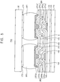
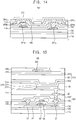
- FIG. 5 is a cross-sectional view illustrating a bonding area of a display device according to an exemplary embodiment.
- FIG. 6 is an enlarged cross-sectional view illustrating the region B of FIG. 5 .
- connection pads CP1 and CP2 are disposed on a base substrate 110 at (e.g., in or on) a bonding area PA2.
- the connection pads CP1 and CP2 may include lower conductive layers CP1a and CP2a, first intermediate conductive layers CP1b and CP2b, second intermediate conductive layers CP1c and CP2c, and upper conductive layers CP1d and CP2d, respectively.
- the lower conductive layer CP1a of a first connection pad CP1 may be formed from the same layer as that of a first gate metal pattern disposed at (e.g., in or on) the display area.
- the lower conductive layer CP1a may be disposed between a first insulation layer 130 and a second insulation layer 140.
- the lower conductive layer CP2a of a second connection pad CP2 may be formed from the same layer as that of a second gate metal pattern disposed at (e.g., in or on) the display area.
- the lower conductive layer CP2a may be disposed between the second insulation layer 140 and a third insulation layer 150.
- the first intermediate conductive layers CP1b and CP2b of the connection pads CP1 and CP2 may be formed from the same layer as that of a first source metal pattern disposed at (e.g., in or on) the display area.
- the first intermediate conductive layers CP1b and CP2b may be disposed between the third insulation layer 150 and a fourth insulation layer.
- the fourth insulation layer may include an inorganic layer 162 without an organic layer.
- the second intermediate conductive layers CP1c and CP2c of the connection pads CP1 and CP2 may be formed from the same layer as that of a second source metal pattern disposed at (e.g., in or on) the display area.
- the second intermediate conductive layers CP1c and CP2c may be disposed on the fourth insulation layer (e.g., the inorganic layer 162 of the fourth insulation layer).
- the upper conductive layers CP1d and CP2d of the connection pads CP1 and CP2 may be formed from the same layer as that of a sensing conductive pattern of the touch-sensing part disposed at (e.g., in or on) the display area.
- the upper conductive layers CP1d and CP2d may be formed from the same layer as that of a second sensing conductive pattern.
- a cladding layer 172 is disposed at (e.g., in or on) the bonding area PA2 to cover at least a portion of the second intermediate conductive layers CP1c and CP2c.
- the cladding layer 172 may be formed from the same layer as that of the fifth insulation layer 170 (e.g., see FIG. 3 ), and may include an organic material.
- the cladding layer 172 may cover at least side surfaces of the second intermediate conductive layers CP1c and CP2c.
- the cladding layer 172 may be disposed between the second intermediate conductive layers CP1c and CP2c, and may cover at least the side surfaces of the second intermediate conductive layers CP1c and CP2c that face each other.
- a passivation layer including an inorganic material may be disposed on the cladding layer 172.
- the passivation layer may be formed from the same layer as that of the lower touch insulation layer 310, the touch intermediate insulation layer 330, or a combination thereof.
- the passivation layer may include a lower passivation layer 312 and an upper passivation layer 332.
- the passivation layer may extend to be partially disposed under the upper conductive layers CP1d and CP2d.
- the passivation layer may partially overlap with each of the upper conductive layers CP1d and CP2d.
- a driving part (e.g., a driver or a driving circuit) DC including a driving chip may be attached to (e.g., bonded on) the bonding area PA2.
- the driving part DC may be attached to (e.g., bonded on) and electrically connected to the connection pads CP1 and CP2 by conductive bonding members BP1 and BP2.
- the conductive bonding members BP1 and BP2 may include (e.g., may be) metal bumps.
- the conductive bonding members BP1 and BP2 may be electrically connected to the connection pads CP1 and CP2 and to connection terminals CT1 and CT2 of the driving part DC, so that driving signals may be transferred to the connection pads CP1 and CP2 from the driving part DC.
- an anisotropic conductive film including conductive balls or the like may be used for the conductive bonding member.
- each of the second intermediate conductive layers CP1c and CP2c may include an upper layer UL, an intermediate layer ML, and a lower layer LL.
- the upper layer UL and the lower layer LL may include a metal having a relatively small ionization tendency, for example, such as titanium.
- the intermediate layer ML may include a metal having a relatively large ionization tendency, for example, such as aluminum.
- the cladding layer 172 covers at least a side surface of the second intermediate conductive layers CP1c and CP2c. Thus, at least a portion of an upper surface of the upper layer UL may be exposed without being covered by the cladding layer 172, and the intermediate layer ML may not be exposed.
- a thickness T2 of the cladding layer 172 may be less than (e.g., smaller than) a thickness T1 of the fifth insulation layer 170 (e.g., see FIG. 3 ).
- a height of an upper surface of the cladding layer 172 may be lower than a height of an upper surface of the upper conductive layers CP1d and CP2d.
- the height of the upper surface of the cladding layer 172 may be lower than a height of an upper surface of the second intermediate conductive layers CP1c and CP2c.
- the thickness T2 of the cladding layer 172 may be less than or equal to 1 ⁇ m (e.g., 1 micro-meter), and may be greater than a thickness of the second intermediate conductive layers CP1c and CP2c.
- FIGS. 7 to 16 are cross-sectional views illustrating a method for manufacturing a display device according to an exemplary embodiment.
- a buffer layer 120 is formed on a base substrate 110 at (e.g., in or on) a display area DA.
- the base substrate 110 may include glass, quartz, silicon, a polymeric material, and/or the like.
- the base substrate 110 may be a flexible substrate including the polymeric material.
- the polymeric material may include polyethylene terephthalate, polyethylene naphthalate, polyether ketone, polycarbonate, polyarylate, polyether sulfone, polyimide, or a combination thereof.
- the buffer layer 120 may prevent or reduce penetration of impurities, humidity, and/or external gas from underneath the base substrate 110, and may planarize an upper surface of the base substrate 110.
- the buffer layer 120 may include an inorganic material such as silicon oxide, silicon nitride, and/or the like, or a combination thereof.
- An active pattern AP is formed on the buffer layer 120.
- the active pattern AP may include a semiconductive material, such as amorphous silicon, polycrystalline silicon (polysilicon), a metal oxide, and/or the like.
- a semiconductive material such as amorphous silicon, polycrystalline silicon (polysilicon), a metal oxide, and/or the like.
- the active pattern AP includes polysilicon, at least a portion of the active pattern AP may be doped with impurities, for example, such as n-type impurities or p-type impurities.
- the active pattern AP may include a metal oxide semiconductor.
- the active pattern AP may include a two-component compound (ABx), a ternary compound (ABxCy), or a four-component compound (ABxCyDz), which may include indium (In), zinc (Zn), gallium (Ga), tin (Sn), titanium (Ti), aluminum (Al), hafnium (Hf), zirconium (Zr), magnesium (Mg), and/or the like.
- the active pattern may include zinc oxide (ZnOx), gallium oxide (GaOx), titanium oxide (TiOx), tin oxide (SnOx), indium oxide (InOx), indium-gallium oxide (IGO), indium-zinc oxide (IZO), indium tin oxide (ITO), gallium zinc oxide (GZO), zinc magnesium oxide (ZMO), zinc tin oxide (ZTO), zinc zirconium oxide (ZnZrxOy), indium-gallium-zinc oxide (IGZO), indium-zinc-tin oxide (IZTO), indium-gallium-hafnium oxide (IGHO), tin-aluminum-zinc oxide (TAZO), indium-gallium-tin oxide (IGTO), and/or the like.
- a first insulation layer 130 is formed on the active pattern AP.
- a first gate metal pattern including a gate electrode GE is formed on the first insulation layer 130.
- the gate electrode GE overlaps with the active pattern AP.
- a second insulation layer 140 is formed to cover the first gate metal pattern.
- a second gate metal pattern including a gate wiring pattern GP is formed on the second insulation layer 140.
- the first insulation layer 130 and the second insulation layer 140 may each include silicon oxide, silicon nitride, silicon carbide, or a combination thereof.
- the first insulation layer 130 and the second insulation layer 140 may include an insulating metal oxide, for example, such as aluminum oxide, tantalum oxide, hafnium oxide, zirconium oxide, titanium oxide, and/or the like.
- the first insulation layer 130 and the second insulation layer 140 may each have a single-layer structure or a multi-layered structure, which may include silicon nitride and/or silicon oxide.
- the first gate metal pattern and the second gate metal pattern may each include gold (Au), silver (Ag), aluminum (Al), copper (Cu), nickel (Ni), platinum (Pt), magnesium (Mg), chromium (Cr), tungsten (W), molybdenum (Mo), titanium (Ti), tantalum (Ta), or an alloy thereof.
- the first gate metal pattern and the second gate metal pattern may each have a single-layer structure or a multi-layered structure including different metal layers that are stacked on one another.
- lower conductive layers of connection pads are formed at (e.g., in or on) the bonding area PA2.
- a lower conductive layer CP1a of a first connection pad may be formed from the same layer as that of the first gate metal pattern, and a lower conductive layer CP2a of a second connection pad may be formed from the same layer as that of the second gate metal pattern.
- the lower conductive layer CP1a of the first connection pad may be disposed between the first insulation layer 130 and the second insulation layer 140, and the lower conductive layer CP2a of the second connection pad may be disposed on the second insulation layer 140.
- the transfer lines TL1 and TL2 illustrated in FIG. 2 may be formed from the same layers as those of the first gate metal pattern and the second gate metal pattern, respectively, and may be connected to (e.g., may be continuously connected to) corresponding lower conductive layers CP1a and CP2a. At least a portion of the transfer lines TL1 and TL2 may be formed from a different layer from those of the gate electrode GE and the gate wiring pattern GP.
- the transfer lines TL1 and TL2 may include a bridge formed from the same layer as that of a first source metal pattern or a second source metal pattern.
- a third insulation layer 150 is formed at (e.g., in or on) the display area DA to cover the second gate metal pattern. Thereafter, a first source metal pattern is formed on the third insulation layer 150.
- the first source metal pattern may include a source electrode SE and a drain electrode DE, which are electrically connected to (e.g., electrically contact) the active pattern AP.
- the source electrode SE and the drain electrode DE may extend (e.g., may pass) through the third insulation layer 150, the second insulation layer 140, and the first insulation layer 130 to be electrically connected to (e.g., to electrically contact) the active pattern AP.
- first intermediate conductive layers of the connection pads are formed at (e.g., in or on) the bonding area PA2.
- a first intermediate conductive layer CP1b of the first connection pad and a first intermediate conductive layer CP2b of the second connection pad may be formed from the same layer as that of the first source metal pattern including the source electrode SE and the drain electrode DE.
- the first intermediate conductive layers CP1b and CP2b may be disposed on the third insulation layer 150.
- first intermediate conductive layer CP1b of the first connection pad may extend (e.g., may pass) through the third insulation layer 150 and the second insulation layer 140 to be electrically connected to the lower conductive layer CP1a.
- the first intermediate conductive layer CP2b of the second connection pad may extend (e.g., may pass) through the third insulation layer 150 to be electrically connected to the lower conductive layer CP2a.
- a fourth insulation layer 160 is formed to cover the first source metal pattern.
- the fourth insulation layer 160 may include an inorganic layer 162 disposed on the first source metal pattern, and an organic layer 164 disposed on the inorganic layer 162.
- the inorganic layer 162 of the fourth insulation layer 160 may be disposed between the first source metal pattern and the organic layer 164 to contact the first source metal pattern, but the present inventive concept is not limited thereto.
- the fourth insulation layer 160 may include the organic layer 164 without the inorganic layer 162.
- a second source metal pattern is formed on the fourth insulation layer 160.
- the second source metal pattern may include a connection electrode CE that is electrically connected to (e.g., that electrically contacts) the drain electrode DE.
- the connection electrode CE may extend (e.g., may pass) through the fourth insulation layer 160 to be electrically connected to (e.g., to electrically contact) the drain electrode DE.
- the second source metal pattern may further include a mesh power line to compensate for a voltage drop of a current applied to an organic light-emitting diode.
- a fifth insulation layer 170 is formed to cover the second source metal pattern.
- the fifth insulation layer 170 may include an opening to expose at least a portion of an upper surface of the connection electrode CE.
- the first source metal pattern and the second source metal pattern may include gold, silver, aluminum, copper, nickel, platinum, magnesium, chromium, tungsten, molybdenum, titanium, tantalum, or an alloy thereof, and may have a single-layer structure or a multi-layered structure including different metal layers.
- the first source metal pattern and the second source metal pattern may include at least a layer including aluminum or aluminum alloy.
- the first source metal pattern and the second source metal pattern may each have a bi-layered structure of titanium/aluminum or a triple-layered structure of titanium/aluminum/titanium.
- each of the third insulation layer 150 and the inorganic layer 162 of the fourth insulation layer 160 may include silicon oxide, silicon nitride, silicon carbide, or a combination thereof.
- the third insulation layer 150 and the inorganic layer 162 of the fourth insulation layer 160 may include an insulating metal oxide, for example, such as aluminum oxide, tantalum oxide, hafnium oxide, zirconium oxide, titanium oxide, or the like.
- the third insulation layer 150 and the inorganic layer 162 of the fourth insulation layer 160 may each have a single-layer structure or a multi-layered structure, which may include silicon nitride and/or silicon oxide.
- the fifth insulation layer 170 and the organic layer 164 of the fourth insulation layer 160 may include an organic insulation material, such as a phenol resin, an acryl resin, a polyimide resin, a polyamide resin, an epoxy resin, benzocyclobutene, and/or the like.
- an organic insulation material such as a phenol resin, an acryl resin, a polyimide resin, a polyamide resin, an epoxy resin, benzocyclobutene, and/or the like.
- second intermediate conductive layers of the connection pads are formed at (e.g., in or on) the bonding area PA2.
- the fourth insulation layer 160 formed on the first intermediate conductive layers CP1b and CP2b may include the inorganic layer 162 without an organic layer (e.g., without the organic layer 164).
- the organic layer 164 disposed at (e.g., in or on) the bonding area PA2 may be removed (e.g., may be entirely removed), or the organic layer 164 may not be disposed at (e.g., in or on) the bonding area PA2.
- the second intermediate conductive layers CP1c and CP2c may be formed on the inorganic layer 162, and may extend (e.g., may pass) through the inorganic layer 162 to be electrically connected to (e.g., to electrically contact) the first intermediate conductive layers CP1b and CP2b, respectively.
- the second intermediate conductive layers CP1c and CP2c may be formed from the same layer as that of the connection electrode CE.
- a cladding layer 172 is formed at (e.g., in or on) the bonding area PA2 to cover at least a portion of the second intermediate conductive layers CP1c and CP2c.
- the cladding layer 172 may be formed from the same layer as that of the fifth insulation layer 170.
- the fifth insulation layer 170 and the cladding layer 172 may be formed by a photolithography process using half-tone light exposure.
- a photoresist composition may be coated at (e.g., in or on) the display area DA and at (e.g., in or on) the bonding area PA2, and the photoresist composition may be exposed to light such that a light amount for an area corresponding to the fifth insulation layer 170 is different from a light amount for an area corresponding to the cladding layer 172.
- the fifth insulation layer 170 and the cladding layer 172 having a thickness different from that of the fifth insulation layer 170 may be formed during the same or substantially the same process.
- a lower electrode layer is formed on the fifth insulation layer 170 and the cladding layer 172, and the lower electrode layer may be patterned to form a first electrode 212 of a light-emitting diode at (e.g., in or on) the display area DA.
- the lower electrode layer 211 may be removed (e.g., may be entirely removed) at (e.g., in or on) the bonding area PA2.
- the lower electrode layer 211 may have a multi-layered structure including a metal oxide layer and a metal layer.
- the metal oxide layer may include, for example, indium tin oxide, indium zinc oxide, zinc tin oxide, indium oxide, zinc oxide, tin oxide, or a combination thereof.
- the metal layer may include, for example, gold, silver, aluminum, copper, nickel, platinum, magnesium, chromium, tungsten, molybdenum, titanium, or a combination thereof.
- the lower electrode layer 211 may include silver.
- silver ions may be dissolved in an etchant during the process of etching the lower electrode layer 211.
- the etchant containing silver ions contact aluminum, which has a larger ionization tendency, silver particles may be formed by Galvanic reduction.
- the silver particles may be transferred to the first electrode 212, may contaminate a strip apparatus, and/or may cause a short between touch-sensing electrodes formed during one or more later processes. Thus, reliability of a display device may be deteriorated.
- the cladding layer 172 covers an aluminum-containing layer of the connection pads.
- the silver particles and problems therefrom discussed above may be prevented or substantially prevented.
- reliability of a display device may be improved.
- a pixel-defining layer 180 is formed at (e.g., in or on) the display area DA.
- the pixel-defining layer 180 may have an opening that exposes at least a portion of the first electrode 212.
- the pixel-defining layer 180 may include an organic insulation material that may be used for forming the fifth insulation layer 170 and/or the like.
- An organic light-emitting layer 214 is formed on the first electrode 212.
- the organic light-emitting layer 214 may be formed at (e.g., in or on) the opening of the pixel-defining layer 180.
- the present inventive concept is not limited thereto.
- the organic light-emitting layer 214 may extend over an upper surface of the pixel-defining layer 180, and/or may be formed as a common layer extending over a plurality of pixels at (e.g., in or on) the display area DA.
- the organic light-emitting layer 214 may include at least a light-emitting layer, and may further include at least one of a hole injection layer (HIL), a hole transporting layer (HTL), an electron transporting layer (ETL), and an electron injection layer (EIL).
- HIL hole injection layer
- HTL hole transporting layer
- ETL electron transporting layer
- EIL electron injection layer
- the organic light-emitting layer 214 may include a low molecular weight organic compound or a high molecular weight organic compound.
- the organic light-emitting layer 214 may emit a red light, a green light, or a blue light. In another exemplary embodiment, the organic light-emitting layer 214 may emit a white light. When the organic light-emitting layer 214 emits a white light, the organic light-emitting layer 214 may have a multi-layered structure including a red-emitting layer, a green-emitting layer, and a blue-emitting layer, or the organic light-emitting layer 214 may have a single-layer structure including a mixture of a red-emitting material, a green-emitting material, and a blue-emitting material.
- a second electrode 216 is formed on the organic light-emitting layer 214.
- the second electrode 216 may be formed as a common layer that extends over a plurality of pixels at (e.g., in or on) the display area DA.
- the second electrode 216 may function as a cathode.
- the second electrode 216 may be formed as a transmitting electrode or a reflecting electrode according to an emission type of the display device.
- the second electrode 216 may include lithium (Li), calcium (Ca), lithium fluoride, aluminum, magnesium, indium tin oxide, indium zinc oxide, zinc tin oxide, indium oxide, zinc oxide, tin oxide, or a combination thereof.
- An encapsulation layer 220 may be disposed on the second electrode 216.
- the encapsulation layer 220 may include a first inorganic thin film 222, an organic thin film 224 disposed on the first inorganic thin film 222, and a second inorganic thin film 226 disposed on the organic thin film 224.
- the organic thin film 224 may include a cured resin, such as polyacrylate and/or the like.
- the cured resin may be formed from crosslinking reaction of monomers.
- the inorganic thin films 222 and 226 may include an inorganic material, such as silicon oxide, silicon nitride, silicon carbide, aluminum oxide, tantalum oxide, hafnium oxide, zirconium oxide, titanium oxide, and/or the like.
- the pixel-defining layer 180, the organic light-emitting layer 214, the second electrode 216, and the encapsulation layer 220 may not be formed at (e.g., in or on) the bonding area PA2, or may be removed at (e.g., in or on) the bonding area PA2.
- a touch-sensing part (e.g., a touch sensor) may be formed on the encapsulation layer 220.
- a lower touch insulation layer 310 may be formed on the encapsulation layer 220.
- a first sensing conductive pattern may be formed on the lower touch insulation layer 310.
- the first sensing conductive pattern may include a bridge pattern 320.
- a touch intermediate insulation layer 330 may be formed on the first sensing conductive pattern.
- a via hole may be formed through the touch intermediate insulation layer 330 to expose the bridge pattern 320.
- a passivation layer is formed on the second intermediate conductive layers CP1c and CP2c and the cladding layer 172 at (e.g., in or on) the bonding area PA2.
- the passivation layer may include a lower passivation layer 312 formed from the same layer as that of the lower touch insulation layer 310, and an upper passivation layer 332 formed from the same layer as that of the touch intermediate insulation layer 330.
- the passivation layer may have via holes exposing the second intermediate conductive layers CP1c and CP2c.
- a second sensing conductive pattern is formed at (e.g., in or on) the display area DA, and upper conductive layers CP1d and CP2d of the connection pads CP1 and CP2 are formed at (e.g., in or on) the bonding area PA2.
- the upper conductive layers CP1d and CP2d may extend (e.g., may pass) through the passivation layer to be electrically connected to (e.g., to electrically contact) the second intermediate conductive layers CP1c and CP2c.
- the lower touch insulation layer 310 and the touch intermediate insulation layer 330 may each include an inorganic insulation material.
- the lower touch insulation layer 310 and the touch intermediate insulation layer 330 may each include silicon oxide, silicon nitride, silicon carbide, or a combination thereof.
- the lower touch insulation layer 310 and the touch intermediate insulation layer 330 may include an insulating metal oxide, for example, such as aluminum oxide, tantalum oxide, hafnium oxide, zirconium oxide, titanium oxide, and/or the like.
- the lower touch insulation layer 310 and the touch intermediate insulation layer 330 may include silicon nitride.
- the first sensing conductive pattern and the second sensing conductive pattern include a conductive material.
- the first sensing conductive pattern and the second sensing conductive pattern may each include a metal, a conductive metal oxide, a conductive polymer, graphene, carbon nano tube, or a combination thereof.
- the metal may include molybdenum, silver, titanium, copper, aluminum, or an alloy thereof.
- the metal may be provided to have a shape of a continuous thin film or a nano wire.
- the conductive metal oxide may include indium tin oxide, indium zinc oxide, zinc tin oxide, indium oxide, zinc oxide, tin oxide, or a combination thereof.
- the first sensing conductive pattern and the second sensing conductive pattern may each have a single-layer structure or a multi-layered structure including different materials.
- a driving part e.g., a driver or a driving circuit
- a driving part DC including a driving chip may be attached to (e.g., may be bonded on) the bonding area PA2.
- the driving part DC may be attached to (e.g., may be bonded on) the bonding area PA2 by hot-pressing, supersonic welding, and/or the like, and may be electrically connected to the connection pads CP1 and CP2 by the conductive bonding members BP1 and BP2.
- the cladding layer 172 including an organic material is not exposed to the exterior (e.g., to the outside).
- the cladding layer 172 may be prevented or substantially prevented from absorbing moisture and/or from swelling in an environment with high humidity and/or high temperature.
- bonding defects for example, such as interface separation of the connection pads and the bonding members, may be prevented or reduced.
- the cladding layer 172 has a reduced thickness.
- protrusion of the cladding layer 172 may be prevented or substantially prevented. Accordingly, effects caused by swelling of the cladding layer 172 may be reduced, and a contact area of the connection pads and the bonding members may be increased.
- FIGS. 17 and 18 are cross-sectional views illustrating a display device according to various exemplary embodiments.
- connection pads CP1 and CP2 disposed at (e.g., in or on) a bonding area PA2 may include lower conductive layers CP1a and CP2a, first intermediate conductive layers CP1b and CP2b, second intermediate conductive layers CP1c and CP2c, third intermediate conductive layers CP1e and CP2e, and upper conductive layers CP1d and CP2d, respectively.
- the lower conductive layer CP1a of a first connection pad CP1 may be formed from the same layer as that of a first gate metal pattern disposed at (e.g., in or on) the display area.
- the lower conductive layer CP1a may be disposed between the first insulation layer 130 and the second insulation layer 140.
- the lower conductive layer CP2a of a second connection pad CP2 may be formed from the same layer as that of a second gate metal pattern disposed at (e.g., in or on) the display area.
- the lower conductive layer CP2a may be disposed between the second insulation layer 140 and the third insulation layer 150.
- the first intermediate conductive layers CP1b and CP2b of the connection pads CP1 and CP2 may be formed from the same layer as that of a first source metal pattern disposed at (e.g., in or on) the display area.
- the first intermediate conductive layers CP1b and CP2b may be disposed between the third insulation layer 150 and the fourth insulation layer.
- the fourth insulation layer may include an inorganic layer 162 without an organic layer.
- the second intermediate conductive layers CP1c and CP2c of the connection pads CP1 and CP2 may be formed from the same layer as that of a second source metal pattern disposed at (e.g., in or on) the display area.
- the second intermediate conductive layers CP1c and CP2c may be disposed on the fourth insulation layer.
- the third intermediate conductive layers CP1e and CP2e of the connection pads CP1 and CP2 may be formed from the same layer as that of a sensing conductive pattern of the touch-sensing part disposed at (e.g., in or on) the display area.
- the third intermediate conductive layers CP1e and CP2e may be formed from the same layer as that of the first sensing conductive pattern.
- the upper conductive layers CP1d and CP2d of the connection pads CP1 and CP2 may be formed from the same layer as that of a sensing conductive pattern of the touch-sensing part disposed at (e.g., in or on) the display area.
- the upper conductive layers CP1d and CP2d may be formed from the same layer as that of the second sensing conductive pattern.
- a cladding layer 172 is disposed at (e.g., in or on) the bonding area PA2 to cover at least a portion of the second intermediate conductive layers CP1c and CP2c.
- the cladding layer 172 may be formed from the same layer as that of a fifth insulation layer disposed at (e.g., in or on) the display area, and may include an organic material.
- the cladding layer 172 may cover at least side surfaces of the second intermediate conductive layers CP1c and CP2c.
- a passivation layer including an inorganic material may be disposed on the cladding layer 172.
- the passivation layer may be formed from the same layer as that of the lower touch insulation layer 310, the touch intermediate insulation layer 330, or a combination thereof.
- the passivation layer may include a lower passivation layer 312 and an upper passivation layer 332. The passivation layer may extend to be partially disposed under the upper conductive layers CP1d and CP2d.
- the third intermediate conductive layers CP1e and CP2e may be partially disposed between the lower passivation layer 312 and the upper passivation layer 332.
- connection pads CP1 and CP2 disposed at (e.g., in or on) a bonding area PA2 may include lower conductive layers CP1a and CP2a, intermediate conductive layers CP1b and CP2b, and upper conductive layers CP1d and CP2d, respectively.
- the lower conductive layer CP1a of a first connection pad CP1 may be formed from the same layer as that of a first gate metal pattern disposed at (e.g., in or on) the display area.
- the lower conductive layer CP1a may be disposed between the first insulation layer 130 and the second insulation layer 140.
- the lower conductive layer CP2a of a second connection pad CP2 may be formed from the same layer as that of a second gate metal pattern disposed at (e.g., in or on) the display area.
- the lower conductive layer CP2a may be disposed between the second insulation layer 140 and the third insulation layer 150.
- the intermediate conductive layers CP1b and CP2b of the connection pads CP1 and CP2 may be formed from the same layer as that of a first source metal pattern or a second source metal pattern, which are disposed at (e.g., in or on) the display area.
- the upper conductive layers CP1d and CP2d of the connection pads CP1 and CP2 may be formed from the same layer as that of a sensing conductive pattern of the touch-sensing part disposed at (e.g., in or on) the display area.
- the upper conductive layers CP1d and CP2d may be formed from the same layer as that of the second sensing conductive pattern.
- a cladding layer 172 is disposed at (e.g., in or on) the bonding area PA2 to cover at least a portion of the intermediate conductive layers CP1b and CP2b.
- the cladding layer 172 may include an organic material.
- the cladding layer 172 may cover at least side surfaces of the intermediate conductive layers CP1b and CP2b.
- a passivation layer including an inorganic material may be disposed on the cladding layer 172.
- the passivation layer may be formed from the same layer as that of the lower touch insulation layer 310, the touch intermediate insulation layer 330, or a combination thereof.
- the passivation layer may include a lower passivation layer 312 and an upper passivation layer 332. The passivation layer may extend to be partially disposed under the upper conductive layers CP1d and CP2d.
- connection pads in one or more exemplary embodiments may have various configurations.
- the present inventive concept is not limited to the examples shown in the exemplary embodiments described herein, and the connection pads may have various suitable or desired configurations as would be known to those skilled in the art within the scope of the present claims.
- a passivation layer at (e.g., in or on) a bonding area may have a single-layer structure.
- a layer for forming an upper conductive layer of a connection pad is not limited to a conductive layer for forming a touch-sensing part (e.g., a touch sensor) with a capacitance type, and a conductive layer for forming a touch-sensing part (e.g., a touch sensor) with various suitable types or sensors may be used for forming the upper conductive layer.
- a layer for forming a cladding layer is not limited to a second via insulation layer.
- the cladding layer may be formed from the same layer as that of a first via insulation layer, or may be formed individually.
- lower conductive layers of a first connection pad and a second connection pad may be formed from the same layer.
- connection pad including an aluminum-containing layer.
- the connection pad may include various suitable or desired metals or alloys thereof.
- One or more exemplary embodiments of the present inventive concept may be applied to various kinds of display devices.
- one or more exemplary embodiments may be applied to a vehicle-display device, a ship-display device, an aircraft-display device, portable communication devices, display devices for display and/or for information transfer, a medical-display device, and/or the like.
Landscapes
- Engineering & Computer Science (AREA)
- Theoretical Computer Science (AREA)
- General Engineering & Computer Science (AREA)
- Microelectronics & Electronic Packaging (AREA)
- Physics & Mathematics (AREA)
- General Physics & Mathematics (AREA)
- Human Computer Interaction (AREA)
- Manufacturing & Machinery (AREA)
- Computer Networks & Wireless Communication (AREA)
- Optics & Photonics (AREA)
- Geometry (AREA)
- Devices For Indicating Variable Information By Combining Individual Elements (AREA)
- Electroluminescent Light Sources (AREA)
Applications Claiming Priority (1)
| Application Number | Priority Date | Filing Date | Title |
|---|---|---|---|
| KR1020190088190A KR20210011529A (ko) | 2019-07-22 | 2019-07-22 | 표시 장치 및 표시 장치의 제조 방법 |
Publications (3)
| Publication Number | Publication Date |
|---|---|
| EP3770965A2 true EP3770965A2 (fr) | 2021-01-27 |
| EP3770965A3 EP3770965A3 (fr) | 2021-05-05 |
| EP3770965B1 EP3770965B1 (fr) | 2024-04-03 |
Family
ID=71728573
Family Applications (1)
| Application Number | Title | Priority Date | Filing Date |
|---|---|---|---|
| EP20186621.7A Active EP3770965B1 (fr) | 2019-07-22 | 2020-07-20 | Afficheur et son procédé de fabrication |
Country Status (5)
| Country | Link |
|---|---|
| US (2) | US11700758B2 (fr) |
| EP (1) | EP3770965B1 (fr) |
| JP (1) | JP7469943B2 (fr) |
| KR (1) | KR20210011529A (fr) |
| CN (1) | CN112289826B (fr) |
Cited By (1)
| Publication number | Priority date | Publication date | Assignee | Title |
|---|---|---|---|---|
| EP4322725A1 (fr) * | 2022-08-08 | 2024-02-14 | Samsung Display Co., Ltd. | Panneau d'affichage et dispositif électronique le comprenant |
Families Citing this family (7)
| Publication number | Priority date | Publication date | Assignee | Title |
|---|---|---|---|---|
| CN113053923A (zh) * | 2021-03-15 | 2021-06-29 | 武汉华星光电半导体显示技术有限公司 | 显示面板和显示装置 |
| US20220365615A1 (en) * | 2021-05-13 | 2022-11-17 | Cambrios Film Solutions Corporation | On-cell touch display and preparing method thereof |
| KR20230003702A (ko) * | 2021-06-29 | 2023-01-06 | 삼성디스플레이 주식회사 | 표시 장치 |
| KR20230003839A (ko) * | 2021-06-30 | 2023-01-06 | 엘지디스플레이 주식회사 | 터치 패널 및 이를 포함하는 터치표시장치 |
| KR20230099264A (ko) * | 2021-12-27 | 2023-07-04 | 엘지디스플레이 주식회사 | 표시 패널 및 이를 포함하는 표시 장치 |
| KR20240036755A (ko) * | 2022-09-13 | 2024-03-21 | 삼성디스플레이 주식회사 | 표시 장치 및 이의 제조 방법 |
| KR20240112623A (ko) * | 2023-01-12 | 2024-07-19 | 엘지디스플레이 주식회사 | 표시 장치 |
Family Cites Families (25)
| Publication number | Priority date | Publication date | Assignee | Title |
|---|---|---|---|---|
| KR100205382B1 (ko) * | 1996-07-22 | 1999-07-01 | 구자홍 | 액정 표시 장치 |
| KR20050097000A (ko) | 2004-03-30 | 2005-10-07 | 엘지.필립스 엘시디 주식회사 | 액정표시장치와 그 제조방법 |
| KR100742376B1 (ko) * | 2005-09-30 | 2007-07-24 | 삼성에스디아이 주식회사 | 패드부 및 그 제조 방법 |
| US8710375B2 (en) * | 2008-03-04 | 2014-04-29 | Sharp Kabushiki Kaisha | Display device substrate, method for manufacturing the same, display device, method for forming multi-layer wiring, and multi-layer wiring substrate |
| US8803861B2 (en) | 2012-02-23 | 2014-08-12 | Qualcomm Mems Technologies, Inc. | Electromechanical systems device |
| KR20140094880A (ko) * | 2013-01-23 | 2014-07-31 | 삼성디스플레이 주식회사 | 표시 장치 및 그 제조 방법 |
| KR102054671B1 (ko) * | 2013-09-27 | 2019-12-11 | 엘지디스플레이 주식회사 | 디스플레이 장치 및 그 제조방법 |
| JP6310668B2 (ja) | 2013-10-02 | 2018-04-11 | 株式会社ジャパンディスプレイ | 表示装置及び表示装置の製造方法 |
| KR20150073297A (ko) | 2013-12-20 | 2015-07-01 | 삼성디스플레이 주식회사 | 박막 트랜지스터, 이를 포함하는 표시 기판 및 표시 기판의 제조 방법 |
| KR102637068B1 (ko) | 2016-06-01 | 2024-02-16 | 삼성디스플레이 주식회사 | 표시 장치 및 이의 제조 방법 |
| US10510821B2 (en) * | 2016-06-10 | 2019-12-17 | Innovation Counsel Llp | Display device |
| KR102654925B1 (ko) * | 2016-06-21 | 2024-04-05 | 삼성디스플레이 주식회사 | 디스플레이 장치 및 이의 제조 방법 |
| KR20180002123A (ko) | 2016-06-28 | 2018-01-08 | 삼성디스플레이 주식회사 | 표시장치 |
| KR102007435B1 (ko) | 2016-08-02 | 2019-08-06 | 삼성디스플레이 주식회사 | 유기발광 표시모듈 및 이를 포함하는 유기발광 표시장치 |
| JP6756538B2 (ja) * | 2016-08-03 | 2020-09-16 | 株式会社ジャパンディスプレイ | 表示装置 |
| KR101926527B1 (ko) * | 2016-09-30 | 2018-12-10 | 엘지디스플레이 주식회사 | 터치 센서를 가지는 유기 발광 표시 장치 및 그 제조 방법 |
| KR102693312B1 (ko) * | 2016-09-30 | 2024-08-07 | 엘지디스플레이 주식회사 | 유기 발광 표시 장치 및 그 제조 방법 |
| KR102810070B1 (ko) | 2016-12-27 | 2025-05-21 | 엘지디스플레이 주식회사 | 표시 장치 |
| KR102438256B1 (ko) * | 2017-06-07 | 2022-08-30 | 엘지디스플레이 주식회사 | 터치 스크린을 갖는 유기 발광 표시 장치 및 이의 제조 방법 |
| KR102370406B1 (ko) * | 2017-07-10 | 2022-03-07 | 삼성디스플레이 주식회사 | 유기 발광 표시 장치 및 유기 발광 표시 장치의 제조 방법 |
| KR102413058B1 (ko) | 2017-10-16 | 2022-06-27 | 삼성디스플레이 주식회사 | 표시 장치 |
| JP6942602B2 (ja) * | 2017-10-19 | 2021-09-29 | 株式会社ジャパンディスプレイ | 表示装置の製造方法 |
| KR102476102B1 (ko) | 2017-11-17 | 2022-12-12 | 삼성디스플레이 주식회사 | 표시 패널 및 이의 제조방법 |
| KR102503732B1 (ko) | 2017-11-30 | 2023-02-27 | 삼성디스플레이 주식회사 | 표시 장치 |
| KR102787594B1 (ko) * | 2019-05-02 | 2025-03-28 | 삼성디스플레이 주식회사 | 표시장치 |
-
2019
- 2019-07-22 KR KR1020190088190A patent/KR20210011529A/ko not_active Ceased
-
2020
- 2020-04-01 JP JP2020065785A patent/JP7469943B2/ja active Active
- 2020-04-22 US US16/855,646 patent/US11700758B2/en active Active
- 2020-07-20 EP EP20186621.7A patent/EP3770965B1/fr active Active
- 2020-07-21 CN CN202010705100.XA patent/CN112289826B/zh active Active
-
2023
- 2023-07-10 US US18/349,943 patent/US12219856B2/en active Active
Cited By (1)
| Publication number | Priority date | Publication date | Assignee | Title |
|---|---|---|---|---|
| EP4322725A1 (fr) * | 2022-08-08 | 2024-02-14 | Samsung Display Co., Ltd. | Panneau d'affichage et dispositif électronique le comprenant |
Also Published As
| Publication number | Publication date |
|---|---|
| US20230363237A1 (en) | 2023-11-09 |
| EP3770965B1 (fr) | 2024-04-03 |
| KR20210011529A (ko) | 2021-02-02 |
| US11700758B2 (en) | 2023-07-11 |
| EP3770965A3 (fr) | 2021-05-05 |
| JP2021018415A (ja) | 2021-02-15 |
| US20210028241A1 (en) | 2021-01-28 |
| JP7469943B2 (ja) | 2024-04-17 |
| CN112289826A (zh) | 2021-01-29 |
| CN112289826B (zh) | 2025-06-27 |
| US12219856B2 (en) | 2025-02-04 |
Similar Documents
| Publication | Publication Date | Title |
|---|---|---|
| US12219856B2 (en) | Display device and method for manufacturing the same | |
| US11177340B2 (en) | Display device and method for manufacturing the same | |
| US12178097B2 (en) | Display device including side terminal disposed along an inclined side surface thereof, and method of manufacturing the same | |
| US11444146B2 (en) | Display device and method for manufacturing the same | |
| CN109994528B (zh) | 显示装置 | |
| US11502158B2 (en) | Display device including fan-out wiring arranged in peripheral area adjacent to display area and also being disposed in sealing area surrounding display area | |
| US11889738B2 (en) | Organic light-emitting display device and method for manufacturing the same | |
| US12501793B2 (en) | Display device and method of manufacturing the same | |
| US12402493B2 (en) | Inorganic layer structure in bending area of display device and method of providing the same | |
| US9911802B2 (en) | Display device and method for manufacturing the same | |
| US20260020452A1 (en) | Display device | |
| US12127444B2 (en) | Display device and method for manufacturing the same | |
| US11586258B2 (en) | Bonding structure and display device including the same | |
| US11569331B2 (en) | Display device including a single layer upper pad of a connection pad and method for manufacturing display device | |
| KR20250131660A (ko) | 표시 장치 |
Legal Events
| Date | Code | Title | Description |
|---|---|---|---|
| PUAI | Public reference made under article 153(3) epc to a published international application that has entered the european phase |
Free format text: ORIGINAL CODE: 0009012 |
|
| STAA | Information on the status of an ep patent application or granted ep patent |
Free format text: STATUS: THE APPLICATION HAS BEEN PUBLISHED |
|
| AK | Designated contracting states |
Kind code of ref document: A2 Designated state(s): AL AT BE BG CH CY CZ DE DK EE ES FI FR GB GR HR HU IE IS IT LI LT LU LV MC MK MT NL NO PL PT RO RS SE SI SK SM TR |
|
| AX | Request for extension of the european patent |
Extension state: BA ME |
|
| PUAL | Search report despatched |
Free format text: ORIGINAL CODE: 0009013 |
|
| AK | Designated contracting states |
Kind code of ref document: A3 Designated state(s): AL AT BE BG CH CY CZ DE DK EE ES FI FR GB GR HR HU IE IS IT LI LT LU LV MC MK MT NL NO PL PT RO RS SE SI SK SM TR |
|
| RIC1 | Information provided on ipc code assigned before grant |
Ipc: H01L 27/12 20060101AFI20210326BHEP Ipc: H01L 27/32 20060101ALI20210326BHEP Ipc: G06F 3/041 20060101ALI20210326BHEP |
|
| STAA | Information on the status of an ep patent application or granted ep patent |
Free format text: STATUS: REQUEST FOR EXAMINATION WAS MADE |
|
| 17P | Request for examination filed |
Effective date: 20211103 |
|
| RBV | Designated contracting states (corrected) |
Designated state(s): AL AT BE BG CH CY CZ DE DK EE ES FI FR GB GR HR HU IE IS IT LI LT LU LV MC MK MT NL NO PL PT RO RS SE SI SK SM TR |
|
| P01 | Opt-out of the competence of the unified patent court (upc) registered |
Effective date: 20230516 |
|
| GRAP | Despatch of communication of intention to grant a patent |
Free format text: ORIGINAL CODE: EPIDOSNIGR1 |
|
| STAA | Information on the status of an ep patent application or granted ep patent |
Free format text: STATUS: GRANT OF PATENT IS INTENDED |
|
| RIC1 | Information provided on ipc code assigned before grant |
Ipc: H10K 102/00 20230101ALI20230925BHEP Ipc: H10K 59/131 20230101ALI20230925BHEP Ipc: H10K 59/12 20230101ALI20230925BHEP Ipc: G06F 3/041 20060101ALI20230925BHEP Ipc: H01L 27/12 20060101AFI20230925BHEP |
|
| INTG | Intention to grant announced |
Effective date: 20231020 |
|
| GRAS | Grant fee paid |
Free format text: ORIGINAL CODE: EPIDOSNIGR3 |
|
| GRAA | (expected) grant |
Free format text: ORIGINAL CODE: 0009210 |
|
| STAA | Information on the status of an ep patent application or granted ep patent |
Free format text: STATUS: THE PATENT HAS BEEN GRANTED |
|
| AK | Designated contracting states |
Kind code of ref document: B1 Designated state(s): AL AT BE BG CH CY CZ DE DK EE ES FI FR GB GR HR HU IE IS IT LI LT LU LV MC MK MT NL NO PL PT RO RS SE SI SK SM TR |
|
| REG | Reference to a national code |
Ref country code: CH Ref legal event code: EP |
|
| REG | Reference to a national code |
Ref country code: DE Ref legal event code: R096 Ref document number: 602020028214 Country of ref document: DE |
|
| REG | Reference to a national code |
Ref country code: IE Ref legal event code: FG4D |
|
| REG | Reference to a national code |
Ref country code: LT Ref legal event code: MG9D |
|
| REG | Reference to a national code |
Ref country code: NL Ref legal event code: MP Effective date: 20240403 |
|
| REG | Reference to a national code |
Ref country code: AT Ref legal event code: MK05 Ref document number: 1673360 Country of ref document: AT Kind code of ref document: T Effective date: 20240403 |
|
| PG25 | Lapsed in a contracting state [announced via postgrant information from national office to epo] |
Ref country code: NL Free format text: LAPSE BECAUSE OF FAILURE TO SUBMIT A TRANSLATION OF THE DESCRIPTION OR TO PAY THE FEE WITHIN THE PRESCRIBED TIME-LIMIT Effective date: 20240403 |
|
| PG25 | Lapsed in a contracting state [announced via postgrant information from national office to epo] |
Ref country code: NL Free format text: LAPSE BECAUSE OF FAILURE TO SUBMIT A TRANSLATION OF THE DESCRIPTION OR TO PAY THE FEE WITHIN THE PRESCRIBED TIME-LIMIT Effective date: 20240403 |
|
| PG25 | Lapsed in a contracting state [announced via postgrant information from national office to epo] |
Ref country code: IS Free format text: LAPSE BECAUSE OF FAILURE TO SUBMIT A TRANSLATION OF THE DESCRIPTION OR TO PAY THE FEE WITHIN THE PRESCRIBED TIME-LIMIT Effective date: 20240803 |
|
| PG25 | Lapsed in a contracting state [announced via postgrant information from national office to epo] |
Ref country code: BG Free format text: LAPSE BECAUSE OF FAILURE TO SUBMIT A TRANSLATION OF THE DESCRIPTION OR TO PAY THE FEE WITHIN THE PRESCRIBED TIME-LIMIT Effective date: 20240403 |
|
| PG25 | Lapsed in a contracting state [announced via postgrant information from national office to epo] |
Ref country code: FI Free format text: LAPSE BECAUSE OF FAILURE TO SUBMIT A TRANSLATION OF THE DESCRIPTION OR TO PAY THE FEE WITHIN THE PRESCRIBED TIME-LIMIT Effective date: 20240403 Ref country code: HR Free format text: LAPSE BECAUSE OF FAILURE TO SUBMIT A TRANSLATION OF THE DESCRIPTION OR TO PAY THE FEE WITHIN THE PRESCRIBED TIME-LIMIT Effective date: 20240403 |
|
| PG25 | Lapsed in a contracting state [announced via postgrant information from national office to epo] |
Ref country code: GR Free format text: LAPSE BECAUSE OF FAILURE TO SUBMIT A TRANSLATION OF THE DESCRIPTION OR TO PAY THE FEE WITHIN THE PRESCRIBED TIME-LIMIT Effective date: 20240704 |
|
| PG25 | Lapsed in a contracting state [announced via postgrant information from national office to epo] |
Ref country code: PT Free format text: LAPSE BECAUSE OF FAILURE TO SUBMIT A TRANSLATION OF THE DESCRIPTION OR TO PAY THE FEE WITHIN THE PRESCRIBED TIME-LIMIT Effective date: 20240805 |
|
| PG25 | Lapsed in a contracting state [announced via postgrant information from national office to epo] |
Ref country code: ES Free format text: LAPSE BECAUSE OF FAILURE TO SUBMIT A TRANSLATION OF THE DESCRIPTION OR TO PAY THE FEE WITHIN THE PRESCRIBED TIME-LIMIT Effective date: 20240403 |
|
| PG25 | Lapsed in a contracting state [announced via postgrant information from national office to epo] |
Ref country code: CZ Free format text: LAPSE BECAUSE OF FAILURE TO SUBMIT A TRANSLATION OF THE DESCRIPTION OR TO PAY THE FEE WITHIN THE PRESCRIBED TIME-LIMIT Effective date: 20240403 |
|
| PG25 | Lapsed in a contracting state [announced via postgrant information from national office to epo] |
Ref country code: AT Free format text: LAPSE BECAUSE OF FAILURE TO SUBMIT A TRANSLATION OF THE DESCRIPTION OR TO PAY THE FEE WITHIN THE PRESCRIBED TIME-LIMIT Effective date: 20240403 |
|
| PG25 | Lapsed in a contracting state [announced via postgrant information from national office to epo] |
Ref country code: PL Free format text: LAPSE BECAUSE OF FAILURE TO SUBMIT A TRANSLATION OF THE DESCRIPTION OR TO PAY THE FEE WITHIN THE PRESCRIBED TIME-LIMIT Effective date: 20240403 |
|
| PG25 | Lapsed in a contracting state [announced via postgrant information from national office to epo] |
Ref country code: LV Free format text: LAPSE BECAUSE OF FAILURE TO SUBMIT A TRANSLATION OF THE DESCRIPTION OR TO PAY THE FEE WITHIN THE PRESCRIBED TIME-LIMIT Effective date: 20240403 |
|
| PG25 | Lapsed in a contracting state [announced via postgrant information from national office to epo] |
Ref country code: PT Free format text: LAPSE BECAUSE OF FAILURE TO SUBMIT A TRANSLATION OF THE DESCRIPTION OR TO PAY THE FEE WITHIN THE PRESCRIBED TIME-LIMIT Effective date: 20240805 Ref country code: PL Free format text: LAPSE BECAUSE OF FAILURE TO SUBMIT A TRANSLATION OF THE DESCRIPTION OR TO PAY THE FEE WITHIN THE PRESCRIBED TIME-LIMIT Effective date: 20240403 Ref country code: NO Free format text: LAPSE BECAUSE OF FAILURE TO SUBMIT A TRANSLATION OF THE DESCRIPTION OR TO PAY THE FEE WITHIN THE PRESCRIBED TIME-LIMIT Effective date: 20240703 Ref country code: LV Free format text: LAPSE BECAUSE OF FAILURE TO SUBMIT A TRANSLATION OF THE DESCRIPTION OR TO PAY THE FEE WITHIN THE PRESCRIBED TIME-LIMIT Effective date: 20240403 Ref country code: IS Free format text: LAPSE BECAUSE OF FAILURE TO SUBMIT A TRANSLATION OF THE DESCRIPTION OR TO PAY THE FEE WITHIN THE PRESCRIBED TIME-LIMIT Effective date: 20240803 Ref country code: HR Free format text: LAPSE BECAUSE OF FAILURE TO SUBMIT A TRANSLATION OF THE DESCRIPTION OR TO PAY THE FEE WITHIN THE PRESCRIBED TIME-LIMIT Effective date: 20240403 Ref country code: GR Free format text: LAPSE BECAUSE OF FAILURE TO SUBMIT A TRANSLATION OF THE DESCRIPTION OR TO PAY THE FEE WITHIN THE PRESCRIBED TIME-LIMIT Effective date: 20240704 Ref country code: FI Free format text: LAPSE BECAUSE OF FAILURE TO SUBMIT A TRANSLATION OF THE DESCRIPTION OR TO PAY THE FEE WITHIN THE PRESCRIBED TIME-LIMIT Effective date: 20240403 Ref country code: ES Free format text: LAPSE BECAUSE OF FAILURE TO SUBMIT A TRANSLATION OF THE DESCRIPTION OR TO PAY THE FEE WITHIN THE PRESCRIBED TIME-LIMIT Effective date: 20240403 Ref country code: CZ Free format text: LAPSE BECAUSE OF FAILURE TO SUBMIT A TRANSLATION OF THE DESCRIPTION OR TO PAY THE FEE WITHIN THE PRESCRIBED TIME-LIMIT Effective date: 20240403 Ref country code: BG Free format text: LAPSE BECAUSE OF FAILURE TO SUBMIT A TRANSLATION OF THE DESCRIPTION OR TO PAY THE FEE WITHIN THE PRESCRIBED TIME-LIMIT Effective date: 20240403 Ref country code: AT Free format text: LAPSE BECAUSE OF FAILURE TO SUBMIT A TRANSLATION OF THE DESCRIPTION OR TO PAY THE FEE WITHIN THE PRESCRIBED TIME-LIMIT Effective date: 20240403 Ref country code: RS Free format text: LAPSE BECAUSE OF FAILURE TO SUBMIT A TRANSLATION OF THE DESCRIPTION OR TO PAY THE FEE WITHIN THE PRESCRIBED TIME-LIMIT Effective date: 20240703 |
|
| REG | Reference to a national code |
Ref country code: DE Ref legal event code: R079 Ref document number: 602020028214 Country of ref document: DE Free format text: PREVIOUS MAIN CLASS: H01L0027120000 Ipc: H10D0086000000 |
|
| REG | Reference to a national code |
Ref country code: DE Ref legal event code: R097 Ref document number: 602020028214 Country of ref document: DE |
|
| PG25 | Lapsed in a contracting state [announced via postgrant information from national office to epo] |
Ref country code: DK Free format text: LAPSE BECAUSE OF FAILURE TO SUBMIT A TRANSLATION OF THE DESCRIPTION OR TO PAY THE FEE WITHIN THE PRESCRIBED TIME-LIMIT Effective date: 20240403 |
|
| PG25 | Lapsed in a contracting state [announced via postgrant information from national office to epo] |
Ref country code: EE Free format text: LAPSE BECAUSE OF FAILURE TO SUBMIT A TRANSLATION OF THE DESCRIPTION OR TO PAY THE FEE WITHIN THE PRESCRIBED TIME-LIMIT Effective date: 20240403 |
|
| PG25 | Lapsed in a contracting state [announced via postgrant information from national office to epo] |
Ref country code: SK Free format text: LAPSE BECAUSE OF FAILURE TO SUBMIT A TRANSLATION OF THE DESCRIPTION OR TO PAY THE FEE WITHIN THE PRESCRIBED TIME-LIMIT Effective date: 20240403 Ref country code: RO Free format text: LAPSE BECAUSE OF FAILURE TO SUBMIT A TRANSLATION OF THE DESCRIPTION OR TO PAY THE FEE WITHIN THE PRESCRIBED TIME-LIMIT Effective date: 20240403 |
|
| PG25 | Lapsed in a contracting state [announced via postgrant information from national office to epo] |
Ref country code: SM Free format text: LAPSE BECAUSE OF FAILURE TO SUBMIT A TRANSLATION OF THE DESCRIPTION OR TO PAY THE FEE WITHIN THE PRESCRIBED TIME-LIMIT Effective date: 20240403 |
|
| PG25 | Lapsed in a contracting state [announced via postgrant information from national office to epo] |
Ref country code: SM Free format text: LAPSE BECAUSE OF FAILURE TO SUBMIT A TRANSLATION OF THE DESCRIPTION OR TO PAY THE FEE WITHIN THE PRESCRIBED TIME-LIMIT Effective date: 20240403 Ref country code: SK Free format text: LAPSE BECAUSE OF FAILURE TO SUBMIT A TRANSLATION OF THE DESCRIPTION OR TO PAY THE FEE WITHIN THE PRESCRIBED TIME-LIMIT Effective date: 20240403 Ref country code: RO Free format text: LAPSE BECAUSE OF FAILURE TO SUBMIT A TRANSLATION OF THE DESCRIPTION OR TO PAY THE FEE WITHIN THE PRESCRIBED TIME-LIMIT Effective date: 20240403 Ref country code: EE Free format text: LAPSE BECAUSE OF FAILURE TO SUBMIT A TRANSLATION OF THE DESCRIPTION OR TO PAY THE FEE WITHIN THE PRESCRIBED TIME-LIMIT Effective date: 20240403 Ref country code: DK Free format text: LAPSE BECAUSE OF FAILURE TO SUBMIT A TRANSLATION OF THE DESCRIPTION OR TO PAY THE FEE WITHIN THE PRESCRIBED TIME-LIMIT Effective date: 20240403 |
|
| PG25 | Lapsed in a contracting state [announced via postgrant information from national office to epo] |
Ref country code: MC Free format text: LAPSE BECAUSE OF FAILURE TO SUBMIT A TRANSLATION OF THE DESCRIPTION OR TO PAY THE FEE WITHIN THE PRESCRIBED TIME-LIMIT Effective date: 20240403 |
|
| PLBE | No opposition filed within time limit |
Free format text: ORIGINAL CODE: 0009261 |
|
| STAA | Information on the status of an ep patent application or granted ep patent |
Free format text: STATUS: NO OPPOSITION FILED WITHIN TIME LIMIT |
|
| REG | Reference to a national code |
Ref country code: CH Ref legal event code: PL |
|
| 26N | No opposition filed |
Effective date: 20250106 |
|
| PG25 | Lapsed in a contracting state [announced via postgrant information from national office to epo] |
Ref country code: LU Free format text: LAPSE BECAUSE OF NON-PAYMENT OF DUE FEES Effective date: 20240720 |
|
| PG25 | Lapsed in a contracting state [announced via postgrant information from national office to epo] |
Ref country code: LU Free format text: LAPSE BECAUSE OF NON-PAYMENT OF DUE FEES Effective date: 20240720 |
|
| PG25 | Lapsed in a contracting state [announced via postgrant information from national office to epo] |
Ref country code: BE Free format text: LAPSE BECAUSE OF NON-PAYMENT OF DUE FEES Effective date: 20240731 Ref country code: CH Free format text: LAPSE BECAUSE OF NON-PAYMENT OF DUE FEES Effective date: 20240731 Ref country code: SI Free format text: LAPSE BECAUSE OF FAILURE TO SUBMIT A TRANSLATION OF THE DESCRIPTION OR TO PAY THE FEE WITHIN THE PRESCRIBED TIME-LIMIT Effective date: 20240403 |
|
| REG | Reference to a national code |
Ref country code: BE Ref legal event code: MM Effective date: 20240731 |
|
| PGFP | Annual fee paid to national office [announced via postgrant information from national office to epo] |
Ref country code: GB Payment date: 20250624 Year of fee payment: 6 |
|
| PGFP | Annual fee paid to national office [announced via postgrant information from national office to epo] |
Ref country code: FR Payment date: 20250624 Year of fee payment: 6 |
|
| PG25 | Lapsed in a contracting state [announced via postgrant information from national office to epo] |
Ref country code: IE Free format text: LAPSE BECAUSE OF NON-PAYMENT OF DUE FEES Effective date: 20240720 |
|
| PG25 | Lapsed in a contracting state [announced via postgrant information from national office to epo] |
Ref country code: SE Free format text: LAPSE BECAUSE OF FAILURE TO SUBMIT A TRANSLATION OF THE DESCRIPTION OR TO PAY THE FEE WITHIN THE PRESCRIBED TIME-LIMIT Effective date: 20240403 |
|
| PGFP | Annual fee paid to national office [announced via postgrant information from national office to epo] |
Ref country code: DE Payment date: 20250624 Year of fee payment: 6 |
|
| PG25 | Lapsed in a contracting state [announced via postgrant information from national office to epo] |
Ref country code: CY Free format text: LAPSE BECAUSE OF FAILURE TO SUBMIT A TRANSLATION OF THE DESCRIPTION OR TO PAY THE FEE WITHIN THE PRESCRIBED TIME-LIMIT; INVALID AB INITIO Effective date: 20200720 |
|
| PG25 | Lapsed in a contracting state [announced via postgrant information from national office to epo] |
Ref country code: IT Free format text: LAPSE BECAUSE OF FAILURE TO SUBMIT A TRANSLATION OF THE DESCRIPTION OR TO PAY THE FEE WITHIN THE PRESCRIBED TIME-LIMIT Effective date: 20240403 |
|
| PG25 | Lapsed in a contracting state [announced via postgrant information from national office to epo] |
Ref country code: HU Free format text: LAPSE BECAUSE OF FAILURE TO SUBMIT A TRANSLATION OF THE DESCRIPTION OR TO PAY THE FEE WITHIN THE PRESCRIBED TIME-LIMIT; INVALID AB INITIO Effective date: 20200720 |