EP3771299A1 - Dehnbare leiterplatte und verfahren zur herstellung einer dehnbaren leiterplatte - Google Patents
Dehnbare leiterplatte und verfahren zur herstellung einer dehnbaren leiterplatte Download PDFInfo
- Publication number
- EP3771299A1 EP3771299A1 EP19772152.5A EP19772152A EP3771299A1 EP 3771299 A1 EP3771299 A1 EP 3771299A1 EP 19772152 A EP19772152 A EP 19772152A EP 3771299 A1 EP3771299 A1 EP 3771299A1
- Authority
- EP
- European Patent Office
- Prior art keywords
- wiring board
- stretchable
- reinforcing member
- layer
- stretchable wiring
- Prior art date
- Legal status (The legal status is an assumption and is not a legal conclusion. Google has not performed a legal analysis and makes no representation as to the accuracy of the status listed.)
- Pending
Links
- 238000004519 manufacturing process Methods 0.000 title claims description 24
- 238000000034 method Methods 0.000 title claims description 21
- 239000004020 conductor Substances 0.000 claims abstract description 101
- 239000012943 hotmelt Substances 0.000 claims abstract description 78
- 230000003014 reinforcing effect Effects 0.000 claims description 127
- 239000004744 fabric Substances 0.000 claims description 66
- 239000000758 substrate Substances 0.000 claims description 50
- 229920001971 elastomer Polymers 0.000 claims description 27
- 239000000806 elastomer Substances 0.000 claims description 25
- 239000010410 layer Substances 0.000 description 235
- 239000000835 fiber Substances 0.000 description 48
- 239000000463 material Substances 0.000 description 37
- 239000002245 particle Substances 0.000 description 14
- 239000011347 resin Substances 0.000 description 14
- 229920005989 resin Polymers 0.000 description 14
- 238000001723 curing Methods 0.000 description 12
- 238000000576 coating method Methods 0.000 description 10
- 239000002390 adhesive tape Substances 0.000 description 8
- 239000004831 Hot glue Substances 0.000 description 7
- 239000011230 binding agent Substances 0.000 description 6
- 238000010438 heat treatment Methods 0.000 description 6
- 229910052709 silver Inorganic materials 0.000 description 5
- 239000004332 silver Substances 0.000 description 5
- JHIVVAPYMSGYDF-UHFFFAOYSA-N cyclohexanone Chemical compound O=C1CCCCC1 JHIVVAPYMSGYDF-UHFFFAOYSA-N 0.000 description 4
- HJOVHMDZYOCNQW-UHFFFAOYSA-N isophorone Chemical compound CC1=CC(=O)CC(C)(C)C1 HJOVHMDZYOCNQW-UHFFFAOYSA-N 0.000 description 4
- 239000002904 solvent Substances 0.000 description 4
- OKTJSMMVPCPJKN-UHFFFAOYSA-N Carbon Chemical compound [C] OKTJSMMVPCPJKN-UHFFFAOYSA-N 0.000 description 3
- XUIMIQQOPSSXEZ-UHFFFAOYSA-N Silicon Chemical compound [Si] XUIMIQQOPSSXEZ-UHFFFAOYSA-N 0.000 description 3
- NIXOWILDQLNWCW-UHFFFAOYSA-N acrylic acid group Chemical group C(C=C)(=O)O NIXOWILDQLNWCW-UHFFFAOYSA-N 0.000 description 3
- 238000005452 bending Methods 0.000 description 3
- 229910052799 carbon Inorganic materials 0.000 description 3
- 230000000694 effects Effects 0.000 description 3
- 229920000728 polyester Polymers 0.000 description 3
- 229920002635 polyurethane Polymers 0.000 description 3
- 239000004814 polyurethane Substances 0.000 description 3
- 238000007639 printing Methods 0.000 description 3
- 239000010703 silicon Substances 0.000 description 3
- 229910052710 silicon Inorganic materials 0.000 description 3
- CUVLMZNMSPJDON-UHFFFAOYSA-N 1-(1-butoxypropan-2-yloxy)propan-2-ol Chemical compound CCCCOCC(C)OCC(C)O CUVLMZNMSPJDON-UHFFFAOYSA-N 0.000 description 2
- VXQBJTKSVGFQOL-UHFFFAOYSA-N 2-(2-butoxyethoxy)ethyl acetate Chemical compound CCCCOCCOCCOC(C)=O VXQBJTKSVGFQOL-UHFFFAOYSA-N 0.000 description 2
- FPZWZCWUIYYYBU-UHFFFAOYSA-N 2-(2-ethoxyethoxy)ethyl acetate Chemical compound CCOCCOCCOC(C)=O FPZWZCWUIYYYBU-UHFFFAOYSA-N 0.000 description 2
- NQBXSWAWVZHKBZ-UHFFFAOYSA-N 2-butoxyethyl acetate Chemical compound CCCCOCCOC(C)=O NQBXSWAWVZHKBZ-UHFFFAOYSA-N 0.000 description 2
- 229920002799 BoPET Polymers 0.000 description 2
- YCKRFDGAMUMZLT-UHFFFAOYSA-N Fluorine atom Chemical compound [F] YCKRFDGAMUMZLT-UHFFFAOYSA-N 0.000 description 2
- 229920000459 Nitrile rubber Polymers 0.000 description 2
- 229910021607 Silver chloride Inorganic materials 0.000 description 2
- 229920006311 Urethane elastomer Polymers 0.000 description 2
- 239000003522 acrylic cement Substances 0.000 description 2
- 229920000800 acrylic rubber Polymers 0.000 description 2
- 239000000654 additive Substances 0.000 description 2
- 239000000853 adhesive Substances 0.000 description 2
- 230000001070 adhesive effect Effects 0.000 description 2
- 239000012790 adhesive layer Substances 0.000 description 2
- WUOACPNHFRMFPN-UHFFFAOYSA-N alpha-terpineol Chemical compound CC1=CCC(C(C)(C)O)CC1 WUOACPNHFRMFPN-UHFFFAOYSA-N 0.000 description 2
- 238000007611 bar coating method Methods 0.000 description 2
- 230000015572 biosynthetic process Effects 0.000 description 2
- 239000011248 coating agent Substances 0.000 description 2
- 239000000470 constituent Substances 0.000 description 2
- 238000001816 cooling Methods 0.000 description 2
- SQIFACVGCPWBQZ-UHFFFAOYSA-N delta-terpineol Natural products CC(C)(O)C1CCC(=C)CC1 SQIFACVGCPWBQZ-UHFFFAOYSA-N 0.000 description 2
- 238000010586 diagram Methods 0.000 description 2
- XXJWXESWEXIICW-UHFFFAOYSA-N diethylene glycol monoethyl ether Chemical compound CCOCCOCCO XXJWXESWEXIICW-UHFFFAOYSA-N 0.000 description 2
- 229940075557 diethylene glycol monoethyl ether Drugs 0.000 description 2
- 238000001035 drying Methods 0.000 description 2
- 239000011737 fluorine Substances 0.000 description 2
- 229910052731 fluorine Inorganic materials 0.000 description 2
- 238000002156 mixing Methods 0.000 description 2
- BASFCYQUMIYNBI-UHFFFAOYSA-N platinum Chemical compound [Pt] BASFCYQUMIYNBI-UHFFFAOYSA-N 0.000 description 2
- 229920000058 polyacrylate Polymers 0.000 description 2
- 230000002787 reinforcement Effects 0.000 description 2
- 239000005060 rubber Substances 0.000 description 2
- 238000007650 screen-printing Methods 0.000 description 2
- 229920002379 silicone rubber Polymers 0.000 description 2
- 239000004945 silicone rubber Substances 0.000 description 2
- HKZLPVFGJNLROG-UHFFFAOYSA-M silver monochloride Chemical compound [Cl-].[Ag+] HKZLPVFGJNLROG-UHFFFAOYSA-M 0.000 description 2
- 238000005507 spraying Methods 0.000 description 2
- 229920003048 styrene butadiene rubber Polymers 0.000 description 2
- 229940116411 terpineol Drugs 0.000 description 2
- 229920001169 thermoplastic Polymers 0.000 description 2
- 239000004416 thermosoftening plastic Substances 0.000 description 2
- XLYOFNOQVPJJNP-UHFFFAOYSA-N water Substances O XLYOFNOQVPJJNP-UHFFFAOYSA-N 0.000 description 2
- 239000002759 woven fabric Substances 0.000 description 2
- 229920000178 Acrylic resin Polymers 0.000 description 1
- 239000004925 Acrylic resin Substances 0.000 description 1
- 229920000742 Cotton Polymers 0.000 description 1
- JOYRKODLDBILNP-UHFFFAOYSA-N Ethyl urethane Chemical compound CCOC(N)=O JOYRKODLDBILNP-UHFFFAOYSA-N 0.000 description 1
- 229920000181 Ethylene propylene rubber Polymers 0.000 description 1
- 244000043261 Hevea brasiliensis Species 0.000 description 1
- 229920000557 Nafion® Polymers 0.000 description 1
- 239000004677 Nylon Substances 0.000 description 1
- 239000005062 Polybutadiene Substances 0.000 description 1
- 239000004698 Polyethylene Substances 0.000 description 1
- 229920000297 Rayon Polymers 0.000 description 1
- KJTLSVCANCCWHF-UHFFFAOYSA-N Ruthenium Chemical compound [Ru] KJTLSVCANCCWHF-UHFFFAOYSA-N 0.000 description 1
- BQCADISMDOOEFD-UHFFFAOYSA-N Silver Chemical compound [Ag] BQCADISMDOOEFD-UHFFFAOYSA-N 0.000 description 1
- ATJFFYVFTNAWJD-UHFFFAOYSA-N Tin Chemical compound [Sn] ATJFFYVFTNAWJD-UHFFFAOYSA-N 0.000 description 1
- 229920002978 Vinylon Polymers 0.000 description 1
- HCHKCACWOHOZIP-UHFFFAOYSA-N Zinc Chemical compound [Zn] HCHKCACWOHOZIP-UHFFFAOYSA-N 0.000 description 1
- 239000000956 alloy Substances 0.000 description 1
- 229910045601 alloy Inorganic materials 0.000 description 1
- 239000004760 aramid Substances 0.000 description 1
- 229920003235 aromatic polyamide Polymers 0.000 description 1
- 229910052797 bismuth Inorganic materials 0.000 description 1
- JCXGWMGPZLAOME-UHFFFAOYSA-N bismuth atom Chemical compound [Bi] JCXGWMGPZLAOME-UHFFFAOYSA-N 0.000 description 1
- 229920005549 butyl rubber Polymers 0.000 description 1
- 239000002131 composite material Substances 0.000 description 1
- 239000012141 concentrate Substances 0.000 description 1
- 230000002708 enhancing effect Effects 0.000 description 1
- PCHJSUWPFVWCPO-UHFFFAOYSA-N gold Chemical compound [Au] PCHJSUWPFVWCPO-UHFFFAOYSA-N 0.000 description 1
- 229910052737 gold Inorganic materials 0.000 description 1
- 239000010931 gold Substances 0.000 description 1
- 230000001788 irregular Effects 0.000 description 1
- 238000010030 laminating Methods 0.000 description 1
- 238000003475 lamination Methods 0.000 description 1
- 239000007769 metal material Substances 0.000 description 1
- 238000012986 modification Methods 0.000 description 1
- 230000004048 modification Effects 0.000 description 1
- 238000012544 monitoring process Methods 0.000 description 1
- 229920003052 natural elastomer Polymers 0.000 description 1
- 229920001194 natural rubber Polymers 0.000 description 1
- 229920001778 nylon Polymers 0.000 description 1
- 230000000149 penetrating effect Effects 0.000 description 1
- 229910052697 platinum Inorganic materials 0.000 description 1
- 229920001084 poly(chloroprene) Polymers 0.000 description 1
- 229920002857 polybutadiene Polymers 0.000 description 1
- 229920006267 polyester film Polymers 0.000 description 1
- 229920001225 polyester resin Polymers 0.000 description 1
- 239000004645 polyester resin Substances 0.000 description 1
- -1 polyethylene Polymers 0.000 description 1
- 229920000573 polyethylene Polymers 0.000 description 1
- 229920005749 polyurethane resin Polymers 0.000 description 1
- 239000002964 rayon Substances 0.000 description 1
- 229910052707 ruthenium Inorganic materials 0.000 description 1
- 238000001881 scanning electron acoustic microscopy Methods 0.000 description 1
- 229910052718 tin Inorganic materials 0.000 description 1
- 238000009941 weaving Methods 0.000 description 1
- 229910052725 zinc Inorganic materials 0.000 description 1
- 239000011701 zinc Substances 0.000 description 1
Images









Classifications
-
- H—ELECTRICITY
- H05—ELECTRIC TECHNIQUES NOT OTHERWISE PROVIDED FOR
- H05K—PRINTED CIRCUITS; CASINGS OR CONSTRUCTIONAL DETAILS OF ELECTRIC APPARATUS; MANUFACTURE OF ASSEMBLAGES OF ELECTRICAL COMPONENTS
- H05K3/00—Apparatus or processes for manufacturing printed circuits
- H05K3/22—Secondary treatment of printed circuits
- H05K3/28—Applying non-metallic protective coatings
-
- H—ELECTRICITY
- H05—ELECTRIC TECHNIQUES NOT OTHERWISE PROVIDED FOR
- H05K—PRINTED CIRCUITS; CASINGS OR CONSTRUCTIONAL DETAILS OF ELECTRIC APPARATUS; MANUFACTURE OF ASSEMBLAGES OF ELECTRICAL COMPONENTS
- H05K1/00—Printed circuits
- H05K1/02—Details
- H05K1/0277—Bendability or stretchability details
- H05K1/0283—Stretchable printed circuits
-
- H—ELECTRICITY
- H05—ELECTRIC TECHNIQUES NOT OTHERWISE PROVIDED FOR
- H05K—PRINTED CIRCUITS; CASINGS OR CONSTRUCTIONAL DETAILS OF ELECTRIC APPARATUS; MANUFACTURE OF ASSEMBLAGES OF ELECTRICAL COMPONENTS
- H05K1/00—Printed circuits
- H05K1/02—Details
- H05K1/03—Use of materials for the substrate
- H05K1/0393—Flexible materials
-
- H—ELECTRICITY
- H05—ELECTRIC TECHNIQUES NOT OTHERWISE PROVIDED FOR
- H05K—PRINTED CIRCUITS; CASINGS OR CONSTRUCTIONAL DETAILS OF ELECTRIC APPARATUS; MANUFACTURE OF ASSEMBLAGES OF ELECTRICAL COMPONENTS
- H05K2201/00—Indexing scheme relating to printed circuits covered by H05K1/00
- H05K2201/05—Flexible printed circuits [FPCs]
- H05K2201/052—Branched
-
- H—ELECTRICITY
- H05—ELECTRIC TECHNIQUES NOT OTHERWISE PROVIDED FOR
- H05K—PRINTED CIRCUITS; CASINGS OR CONSTRUCTIONAL DETAILS OF ELECTRIC APPARATUS; MANUFACTURE OF ASSEMBLAGES OF ELECTRICAL COMPONENTS
- H05K2201/00—Indexing scheme relating to printed circuits covered by H05K1/00
- H05K2201/20—Details of printed circuits not provided for in H05K2201/01 - H05K2201/10
- H05K2201/2009—Reinforced areas, e.g. for a specific part of a flexible printed circuit
Definitions
- the present invention relates to a stretchable wiring board and a method for manufacturing the stretchable wiring board.
- Patent Application No. 2018-50527 filed with Japan Patent Office on March 19, 2018, and Patent Application No. 2018-50529 , filed with Japan Patent Office on March 19, 2018 are incorporated herein by reference and are regarded as a part of the description of this specification .
- the wearable device and the medical device are provided in clothes and outfits, and sensing and monitoring are performed by a user wearing these clothes and braces. For this reason, an stretchable wiring board capable of expanding and contracting in accordance with the movement of the human body is used for these devices.
- a stretchable wiring board comprising a sheet-like stretchable substrate having stretchability, a stretchable wiring portion formed on at least one side of a main surface of a stretchable substrate, and an external terminal connected to the wiring portion (for example, see Patent Document 1).
- the unevenness of the main surface of the stretchable wiring board is increased due to the differences caused by the wiring portion and the external terminal protruding from the main surface of the stretchable substrate. Therefore, there are problems that the wearable device gave the user a sense of discomfort and the unevenness was caught.
- the exposed surface of the connection portion and the surface of the overcoat layer are flush with each other, it is possible to reduce unevenness of the main surface of the stretchable wiring board.
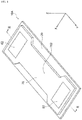
- Fig. 1 is a perspective view showing an stretchable wiring board according to a first embodiment of the present invention
- Fig. 2 is a plan view showing an stretchable wiring board according to the first embodiment of the present invention
- Fig. 3 is a cross-sectional view taken along III-III line of Fig. 1
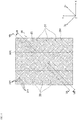
- Fig. 4 is a plan view showing an stretchable substrate according to the first embodiment
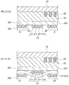
- Fig. 5 (A) is a cross-sectional view taken along VA-VA line of Fig. 4
- Fig. 5 (B) is a cross-sectional view taken along VB-VB line of Fig. 4 .
- the stretchable wiring board 10A shown in Figs. 1 and 2 is used, for example, in a portion where stretchability is required in a wearable device such as a biological sensor and a medical device such as a biological information monitor. Since the wearable device and the medical device are provided on clothes and braces, it is necessary for the stretchable wiring board 10A to sufficiently follow the bending of the human body.
- the use of the stretchable wiring board 10A is not particularly limited as long as the stretchability is required.
- the stretchable wiring board 10A is provided with, for example, electronic components.
- the electronic component a pressure sensitive sensor or silver/silver chloride electrode are formed, or a mounted component such as an integrated circuits (IC), a condenser, or a light emitting diode (LED) are mounted.
- IC integrated circuits
- LED light emitting diode
- the stretchable wiring board 10A of the present embodiment includes a fabric 20, a hot-melt layer 30A, a first reinforcing member 40A, a primer layer 50, a conductor portion 60, and an overcoat layer 70.
- the “stretchable wiring board 10A” in the present embodiment corresponds to an example of the “stretchable wiring board” in the present invention
- the “fabric 20” in the present embodiment corresponds to an example of the “fabric” in the present invention
- the “hot-melt layer 30A” in the present embodiment corresponds to an example of the "first stretchable substrate” in the present invention
- the "first reinforcing member 40A” in the present embodiment corresponds to an example of the “first reinforcing member” in the present invention
- the “primer layer 50 “ in the present embodiment corresponds to an example of the “primer layer” in the present invention
- the “conductor portion 60 “ in the present embodiment corresponds to an example of the “conductor portion” in the present invention
- the “overcoat layer 70 “ in the present embodiment corresponds to an example of the "overcoat layer” in the present invention.
- the fabric 20 is an object to which the hot-melt layer 30A is to be stuck, and is a fabric portion of a garment or a brace provided with a wearable device or the like.
- This fabric 20 is composed of a woven fabric composed of a plurality of fibers, and more specifically as shown in Fig. 4 , is constituted by a first fiber bundle 21 and a second fiber bundle 22 which intersect each other.
- the first fiber bundle 21 is composed of one or more first fibers 211 assembled together.
- the first fiber bundle 21 extends in a direction D 1 (hereinafter, also referred to as a first direction D 1 ) that is inclined with respect to the Y direction in the figure (the stretching and contracting direction of the stretchable circuit board 10A), and the plurality of first fiber bundles 21 are parallel to a direction D 2 (hereinafter, also referred to as a second direction D 2 ) that intersects with the first direction D 1 .
- the second fiber bundle 22 is composed of one or more second fibers 221.
- the second fiber bundle 22 extends in a second directional D 2 , and the plurality of second fiber bundles 22 are parallel to the first directional D 1 .
- the fabric 20 is constituted by weaving first fiber bundles 21 and second fiber bundles 22 with each other in a plan view.
- first fiber 211 and the 2 fiber 22 for example, rayon, nylon, polyester, acrylic, polyurethane, vinylon, polyethylene, Nafion (registered trademark), aramid, cotton, or the like can be used.
- the first fiber 211 and the second fiber 221 may have stretchability.
- the first fiber 211 and the second fiber 221 may be the same or different from each other. Further, the amount of the first fiber 211 and the amount of the second fiber 221 may be the same or different from each other.
- a rectangular gap 23 is formed between the first fiber bundle 21 and the second fiber bundle 22 crossing each other.
- the gap 23 is defined by first fiber bundles 21 and 21 adjacent to each other and second fiber bundles 22 and 22 adjacent to each other.
- the gap 23 opens to one major surface 201 of the fabric 20 and the other major surface 202 (see Figs. 5A and 5B ) of the fabric 20, and communicates one major surface 201 with the other major surface 202 of the fabric 20.
- the gap 23 may not extend straight along thickness of the fabric 20, but may open at both major surfaces 201, 202 and communicate with both major surfaces 201, 202. Since the gap 23 is deformed in accordance with the deformation of the stretchable wiring board 10A, the fabric 20 as a whole exhibits stretchability.
- the Young's modulus Ef of the fabric 20 is preferably 0.1 to 35MPa (0.1MPa ⁇ E f ⁇ 35MPa). Further, the rupture elongation Bf of the fabric 20 is preferably 50% or more (Bf ⁇ 50%). It should be noted that “rupture elongation” means the elongation of the material up to the point of break relative to its natural length. Further, thickness T f of the fabric 20 is preferably 20 to 300 ⁇ m (20 ⁇ m ⁇ T f ⁇ 300 ⁇ m).
- the entire shape of the fabric 20 is rectangular, but is not particularly limited thereto.
- the entire shape of the fabric 20 will vary depending on the shape of the cloth or the brace in which the wearable device is provided.
- the hot-melt layer 30A is affixed to the main surface 201 of the fabric 20, as shown in Fig. 3 , and is formed on the fabric 20. As shown in Figs. 5A and 5B , the hot-melt layer 30A is in close contact with the first fibers 211 and the second fibers 221 located on the main surface 201 of the fabric 20, and enters between the first fibers 211 constituting one first fiber bundle 21 and between the second fibers 221 constituting one second fiber bundle 22.
- This hot-melt layer 30A is slightly impregnated in the vicinity of the surface of the first fiber 211 and the second fiber 221 in contact, but is not impregnated into the interior of the first fiber 211 and the second fiber 221. In other words, in this embodiment, the hot-melt layer 30A is not completely impregnated to the inside of the first fiber 211 and the second fiber 221.
- This hot-melt layer 30A is formed in a bridge shape between adjacent first fiber bundles 21 through a gap 23. Similarly, the hot-melt layer 30A is formed in a bridge shape between adjacent second fiber bundles 22 through the gap 23. As a result, the hot-melt layer 30A covers the gap 23 that opens to the main surface 201 of the fabric 20. Further, the hot-melt layer 30A does not enter the interior of the gap 23, and the interior of the gap 23 is not filled with the hot-melt layer 30A. Note that the hot-melt layer 30A may slightly enter the interior of the gap 23 in the vicinity of the opening of the gap 23 as long as the hot-melt layer 30A does not fill the interior of the gap 23.
- the hot-melt layer 30A has stretchability, and as a constituent material thereof, a hot melt-based resin material such as polyester, polyurethane, acrylic, styrene butadiene rubber, or silicon can be used.
- a hot melt-based resin material such as polyester, polyurethane, acrylic, styrene butadiene rubber, or silicon can be used.
- the first reinforcing member 40A is located between the hot-melt layer 30A and the primer layer 50, in the present embodiment is buried in the hot-melt layer 30A. Further, the conductor portion 60 is positioned above the first reinforcing member 40A via the primer layer 50. In other words, the first reinforcing member 40A is interposed between the hot-melt layer 30A and the conductor portion 60.
- the connection portion 62 of the present embodiment corresponds to the "connection portion" of the present invention.
- the first reinforcing member 40A is disposed so as to overlap the connection portion 62 when viewed from the thickness direction of the conductor portion 60 (is Z direction in Figs., is also the thickness direction of the stretchable wire board 10A).
- the first reinforcing member 40A disposed in this manner particularly reinforces the connection portion 62. Since an external device is connected in the connection portion 62, the connection portion 62 is easily stressed. It is possible to prevent damage to the connection portion 62 by reinforcement by the first reinforcing member 40A.
- the first reinforcing member 40A is buried in the hot-melt layer 30A, even if the first reinforcing member 40A is disposed, a difference in level does not occur on the stretchable wiring board 10A.
- the smoothness of both main surfaces of the stretchable wiring board 10A can be improved.
- the first reinforcing member 40A is interposed between the hot-melt layer 30A and the conductor portion 60, and the first reinforcing member 40A is disposed at a position close to the conductor portion 60. Therefore, the connection portion 62 can be reliably reinforced.
- the first reinforcing member 40A is not particularly limited, but for example, an adhesive tape or the like can be used as the first reinforcing member.
- the adhesive tape is not particularly limited, but for example, an adhesive tape composed of a polyester film with an acrylic adhesive layer on its main surface can be used. In this case, the first reinforcing member 40A is disposed by sticking the acrylic adhesive layer to the primer layer 50.
- the primer layer 50 is provided on the hot-melt layer 30A and the first reinforcing member 40A, and is interposed between the hot-melt layer 30A and the conductor portion 60.
- the primer layer 50 covers the lower surface 601 and the side surface 602 of the conductor portion 60, and the planar shape of the primer layer 50 is substantially the same as the planar shape of the conductor portion 60. Further, the primer layer 50 has stretchability similarly to the fabric 20 and the like.
- the primer layer 50 functions as a buffer layer for preventing breakage of the conductor portion 60 and as a waterproof layer when the stretchable wiring board 10A is extended.
- a polyester resin, a polyurethane resin, an acrylic resin, or a silicon resin can be exemplified.
- the Young's modulus E p of the primer layer 50 is preferably less than or equal to the Young's modulus E f of the fabric 20 (E p ⁇ E f ), and is more preferably lower than the Young's modulus E f of the fabric 20 (E p ⁇ E f ) from the viewpoint of enhancing the function as the buffer layer between the fabric 20 and the conductor portion 60.
- the Young's modulus E p of the primer layer 50 is preferably 0.1 to 10MPa (0. 1MPa ⁇ E p ⁇ 10MPa).
- the rupture elongation B p of of the primer layer 50 is preferably 50% or more (B p ⁇ 50%).
- the thickness T p of the primer layer 50 is preferably 10 to 50 ⁇ m (10 ⁇ m ⁇ T P ⁇ 50 ⁇ m).
- the conductor portion 60 is provided on the primer layer 50.
- the conductor portion 60 includes a wiring portion 61 covered with the overcoat layer 70 and a connection portion 62 exposed to the outside from the overcoat layer 70. That is, the wiring portion 61, which is a part of the conductor portion 60, is interposed between the hot-melt layer 30A and the overcoat layer 70.
- the "wiring portion 61" in the present embodiment corresponds to the "wiring portion” in the present invention
- the "connection portion 62 " in the present embodiment corresponds to the "connection portion” in the present invention.
- Wiring portion 61 is integrally formed with the connection portion 62, and electrically connects the plurality of connection portions 62 to each other.
- the wiring portion 61 has a single strip-shaped planar shape, but is not limited thereto.
- the wiring portion 61 may have an arbitrary pattern such as a branched planar shape depending on the application of the stretchable wiring board 10A.
- connection portion 62 has a convex protruding portion 621 protruding in a direction away from the hot-melt layer 30A.
- An exposed surface 622 of the protruding portion 621 is exposed from the overcoat layer 70.
- the "exposed surface 622 " of the present embodiment corresponds to the "exposed surface” of the present invention.
- connection portion 62 can be used as a connection terminal with an electronic device, and conduction with the electronic device is ensured on the exposed surface 622.
- the embodiment exemplifies a mode in which two connection portions 62 are provided, the present invention is not limited to this, and three or more connection portions 62 may be provided depending on the use of the stretchable wiring board 10A.
- the conductor portion 60 is formed by dispersing conductive particles in a binder, and has stretchability.
- the stretchability is imparted to the conductor portion 60 by the binder contained in the conductor portion 60 is made of a material having stretchability.
- an elastomer as the binder, and for example, acrylic rubber, urethane rubber, nitrile rubber, silicone rubber, fluorine rubber, these two or more composites or the like can be used as the elastomer.
- a metal material such as gold, silver, platinum, ruthenium, lead, tin, zinc, bismuth, or an alloy thereof, or a nonmetallic material such as carbon can be used.
- the shape of the conductive particles is preferably a scaly shape or an indefinite shape.
- the conductive particles included in the protrusion 621 may be different types of conductive particles included in the wiring portion 61.
- carbon may be used as the conductive particles included in the projecting portion 621
- silver may be used as the conductive particles included in the wiring portion 61.
- the Young's modulus E c of the conductor portion 60 is preferably high than the Young's modulus Ef of the fabric 20 (E c >E f ).
- the Young's modulus E c of the conductor portion 60 is preferably 10 to 200MPa (10MPa ⁇ E c ⁇ 200MPa).
- the maximum extensibility LE c of the conductor portion 60 is preferably 5 to 50% (5% ⁇ LE c ⁇ 50%). Further, as the rupture elongation B c of the conductor portion 60 is preferably 10 to 100% (10% ⁇ B c ⁇ 100%).
- the overcoat layer 70 is provided on the conductor portion 60 and the primer layer 50, and protects the conductor portion 60 by covering at least a part of the conductor portion 60. Specifically, the upper surface and the side surface of the protrusion 621 of the wiring portion 61 is covered with the overcoat layer 70. A hole 701 penetrating from one main surface to the other main surface of the overcoat 70 is formed, and a protrusion 621 is formed inside the hole 701.
- the surface 702 of the overcoat layer 70 which is a main surface of the overcoat layer 70 that is not in contact with the conductor portion 60, is flush with the exposed surface 622 of the connection portion 62.
- flush means that the surface 702 of the overcoat layer 70 and the exposed surface 622 of the connection portion 62 are located on the same plane, or that size D of a difference in level is 5 ⁇ m or less (0 ⁇ m ⁇ D ⁇ 5 ⁇ m). In particular, it is more preferable that the size D of a difference in level is 1 ⁇ m or less (0 ⁇ m ⁇ D ⁇ 1 ⁇ m).
- the overcoat layer 70 preferably has stretchability.
- polyester, polyurethane, acrylic, silicon, or the like can be exemplified.
- the Young's modulus E o of the overcoat layer 70 is preferably high than the Young's modulus E p of the primer layer 50 (E o >E p ), more preferably lower than the Young's modulus E c of the transducer portion 60 (E o ⁇ E c ).
- the Young's modulus E o of the overcoat layer 70 is preferably 5 to 100MPa (5MPa ⁇ E o ⁇ 100MPa).
- the maximum extensibility LE o of the overcoat layer 70 is preferably 10 to 50% (10% ⁇ LE o ⁇ 50%).
- the breaking elongation B o of the overcoat layer 70 is preferably 50% or more (B o ⁇ 50%).
- thickness T o of the overcoat layer 70 is preferably 10 to 20 ⁇ m (10 ⁇ m ⁇ T o ⁇ 20 ⁇ m).
- the material constituting the overcoat layer 70 and the material constituting the primer layer 50 are substantially the same material.
- the interface between the primer layer 50 and the overcoat layer 70 is slightly visible, and the primer layer 50 and the overcoat layer 70 are substantially integrated.
- an stretchable substrate (not shown) may be affixed on the overcoat layer 70 so as to cover the interface between the overcoat layer 70 and the connection portion 62.
- a resin material can be used, and it is preferable that this resin material has a waterproof property.
- the resin material having this waterproof property is not particularly limited, but a seam tape can be used.
- a release film 80 which will be described later, may be attached to the overcoat layer 70 (see Fig. 7 (g) ).
- the stretchable wiring board 10A of the present embodiment as described above has the following effects.
- the stretchable wiring board 10A since the surface 702 of the overcoat layer 70 and the exposed surface 622 of the connection portion 62 are flush with each other, it is possible to reduce unevenness on the surface of the stretchable wiring board 10A to such an extent that the user does not feel uncomfortable in the wearable device or the like.
- the hot-melt layer 30A exhibits fluidity by being heated, for example at the time of sticking to the fabric 20. Due to the fluidity of the hot-melt layer 30A, it is possible to absorb the irregularities on the surface of the fabric 20, and also to absorb the difference in level between the primer layer 50 and the first reinforcing member 40A, so that it is possible to reduce the unevenness as a whole of the stretchable wiring board 10A.
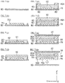
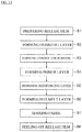
- Fig. 6 is a flow sheet for explaining the method of manufacturing the stretchable wiring board according to the present embodiment.
- Figs. 7(a) to 7 (h) are diagrams showing respective steps of Fig. 6 , specifically, Fig. 7(a) is a cross-sectional view for explaining a step of preparing the release film, Fig. 7(b) is a cross-sectional view for explaining a step of forming the overcoat layer, Fig. 7(c) is a cross-sectional view for explaining a step of forming the conductor portion, Fig.
- Fig. 7 (d) is a cross-sectional view for explaining a step of forming the primer layer
- Fig. 7 (e) is a cross-sectional view for explaining a step of disposing the first reinforcing member
- Fig. 7 (f) is a cross-sectional view for explaining a step of forming the hot-melt layer
- Fig. 7 (g) is a cross-sectional view for explaining a step of attaching the fabric
- Fig. 7 (h) is a cross-sectional view for explaining a step of peeling the release film.
- the method of manufacturing the stretchable wiring board of the present embodiment includes the step of preparing the release film (a step S1), the step of forming the overcoat layer (a step S2), the step of forming a conductor portion (a step S3), the step of forming the primer layer (a step S4), the step of arranging the first reinforcing member (a step S5), the step of forming the hot-melt layer (a step S6), the step of attaching the fabric (a step S7), and the step of peeling the release film (a step S8).
- the release film 80 is prepared.
- This release film 80 is a resin film subjected to a release process, and is not particularly limited, and for example, a release treatment PET film can be used as the release film 80.
- the step S1 in this embodiment corresponds to the "first step" of the present invention.
- the overcoat layer 70 having a predetermined pattern is formed on one main surface of the release film 80.
- the holes 701 in which the overcoat layer 70 is not formed on the release film 80 are also formed at the same time.
- the overcoat layer 70 is formed by coating the material constituting the overcoat layer 70 described above on the release film 80 and curing the material.
- various coating methods such as a screen printing method, a spray coating method, a bar coating method, a dip method, and an inkjet method can be employed.
- step S2 in this embodiment corresponds to the "second step" of the present invention.
- the conductor portion 60 is formed.
- the connection portion 62 is formed in the inside of the hole 701
- the wiring portion 61 is formed on the overcoat layer 70.
- the conductor portion 60 is formed by applying a conductive paste to the inside of the hole 701 and on the overcoat layer 70, and curing the conductive paste.
- Specific examples of the conductive paste for forming the conductor portion 60 may be exemplified by conductive particles, a binder, water or a solvent, and a conductive paste constituting by mixing various additives.
- the solvent contained in the conductive paste examples include butyl cellosolve acetate, carbitol acetate, butyl carbitol acetate, dipropylene glycol monobutyl Ether, diethylene glycol monoethyl Ether, cyclohexanone, isophorone, and terpineol.
- the coating method and the curing method the same method as in the case of forming the overcoat layer 70 can be used.
- the step S3 in the present embodiment corresponds to the "third step of forming the connection portion on the release film” and the "fourth step of forming the wiring portion on the overcoat layer” of the present invention.
- the "third step” and the "fourth step” of the present invention are simultaneously performed.
- the primer layer 50 is formed on the conductor portion 60.
- the primer layer 50 is formed by applying the above-described resin material to the conductor portion 60 and curing the resin material.
- the coating method and the curing method the same method as in the case of forming the overcoat layer 70 can be used.
- the first reinforcing member 40A is disposed on the primer layer 50.
- the first reinforcing member 40A when viewed from the thickness direction of the conductor portion 60, disposed at a position overlapping the connection portion 62.
- the first reinforcing member 40A is formed by preparing the above-described adhesive tape and sticking the adhesive layer of the adhesive tape to the primer layer 50.
- the hot-melt layer 30A is formed on the first reinforcing member 40A and the primer layer 50.
- the hot-melt layer 30A can be formed by placing the above-described thermoplastic hot-melt adhesive on the first reinforcing member 40A and the primer layer 50. At this time, the hot-melt adhesive may be heated and molded into an arbitrary shape. Further, a sheet-like hot-melt adhesive may be used as this adhesive.
- the step S6 in this embodiment corresponds to the "fifth step" of the present invention.
- the fabric 20 is affixed to the hot-melt layer 30A.
- the hot-melt layer 30A in a state in which is softened by heating is affixed to the fabric 20.
- the step S7 in this embodiment corresponds to the "sixth step" of the present invention.
- the release film 80 is peeled from the stretchable wiring board 10A.
- the step S8 in this embodiment corresponds to the "seventh step" of the present invention.
- the timing at which the release film 80 is peeled off is not limited only after the fabric 20 is affixed.
- the release film 80 may be peeled off after the formation of the hot-melt layer 30A (after the step S6 in Fig. 6 ) and before the affixing of the fabric 20 (before the step S7 in Fig. 6 ).
- the both surfaces are smooth and it is possible to prevent the occurrence of a difference in level at both boundaries (the both surfaces are flush with each other). As a result, the unevenness on the surface of the stretchable wiring board can be reduced to the extent that the user of the wearable device or the like does not feel uncomfortable.
- Fig. 8 is a plan view of an stretchable wiring board in the first embodiment of the present invention
- Fig. 9 is a sectional view taken along IX-IX line of Fig. 8
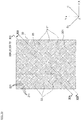
- Fig. 10 is an enlarged view of the X portion of Fig. 8
- Fig.11 (A) is a cross-sectional view taken along XIA-XIA line of Fig. 10
- Fig. 11 (B) is a cross-sectional view taken along XIB-XIB line of Fig. 10
- Fig. 12 is a plan view for explaining the conductor portion of the stretchable wiring board.
- Fig. 9 is a sectional view taken along IX-IX line of Fig. 8
- Fig. 10 is an enlarged view of the X portion of Fig. 8
- Fig.11 (A) is a cross-sectional view taken along XIA-XIA line of Fig. 10
- Fig. 11 (B) is a cross-sectional
- the stretchable wiring board 10B shown in Figs. 8 and 9 is used, for example, in the wearable device such as the biometric sensor or a medical device such as the biometric information monitor in a portion where the stretchability is required, same to the first embodiment. Since the wearable device and the medical device are provided on clothes and the braces, it is necessary for the stretchable wiring board 10B to sufficiently follow the bending of the human body.
- the electronic component 200 is provided on such stretchable wiring board 10B.
- a pressure sensitive sensor or silver/silver chloride electrode are formed, or a mounted component such as an integrated circuits (IC), a condenser, or a light emitting diode (LED) are mounted.
- IC integrated circuits
- LED light emitting diode
- the use of the stretchable wiring board 10B is not particularly limited as long as it requires an stretchable property.
- the stretchable wiring board 10B of the present embodiment includes a fabric 20, a hot-melt layer 30A, a first reinforcing member 40A, a second reinforcing member 40B, a primer layer 50, a conductor portion 60, and an overcoat layer 70.
- the “stretchable wiring board 10B" in the present embodiment corresponds to an example of the “stretchable wiring board” in the present invention
- the “fabric 20” in the present embodiment corresponds to an example of the “fabric” in the present invention
- the "hot-melt layer 30A” in the present embodiment corresponds to an example of the "first stretchable base material” in the present invention
- the "first reinforcing member 40A” in the present embodiment corresponds to an example of the “first reinforcing member” in the present invention
- the “second reinforcing member 40B” in the present embodiment corresponds to an example of the “second reinforcing member” in the present invention
- the "primer layer 50 " in the present embodiment corresponds to an example of the “primer layer” in the present invention
- the “conductor portion 60 “ in the present embodiment corresponds to an example of the “conductor portion” in the present invention
- the "overcoat layer 70 “ in the present embodiment corresponds to an example of the "overcoat layer”
- the fabric 20 is an object to which the hot-melt layer 30A is to be affixed, and is a fabric portion of a garment or a brace provided with a wearable device or the like.
- this fabric 20 is composed of a woven fabric composed of a plurality of fibers, and more specifically, is constituted by a first fiber bundle 21 and a second fiber bundle 22 which intersect each other as shown in an enlarged view of Fig. 10 .
- a rectangular gap 23 is formed between the first fiber bundle 21 and the second fiber bundle 22 crossing each other.
- the gap 23 is defined by first fiber bundles 21 and 21 adjacent to each other and second fiber bundles 22 and 22 adjacent to each other.
- the gap 23 opens to one main surface 201 of the fabric 20 and opens to the other main surface 202 (see Figs. 11A and 11B ) of the fabric 20, and communicates between the one main surface 201 and the other main surface 202 of the fabric 20.
- the gap 23 may not extend straight along thickness of the fabric 20, but may open at both major surfaces 201, 202 and communicate with both major surfaces 201, 202.
- the gap 23 is deformed in accordance with the modification of the stretchable wiring board 10B, whereby the fabric 20 as a whole exhibits stretchability.
- the hot-melt layer 30A is affixed to the main surface 201 of the fabric 20 as shown in Figs. 11 (A) and 11 (B) , and is formed on the fabric 20 as in the first embodiment.
- This hot-melt layer 30A has stretchability, and as a constituent material thereof, the same material as in the first embodiment can be used.
- the first reinforcing member 40A is disposed so as to overlap the connection portion 62 when viewed from thickness direction of the conductor portion 60.
- This first reinforcing member 40A is buried in the hot-melt layer 30A, and is interposed between the hot-melt layer 30A and the primer layer 50. Since an external device is connected in the connection portion 62, the connection portion 62 is easily stressed. It is possible to prevent damage to the connection portion 62 by reinforcement by the first reinforcing member 40A.
- connection portion 62 can be reliably reinforced.
- the "connection portion 62 " in the present embodiment corresponds to the "connection portion" in the present invention.
- distance L A between the first reinforcing member 40A and the second reinforcing member 40B adjacent to the first reinforcing member 40A satisfies the following equation (1). 50 mm ⁇ L A ⁇ 200 mm
- first reinforcing member 40A an adhesive tape or the like can be used.
- the second reinforcing member 40B (the second reinforcing member 40B 1 and the second reinforcing member 40B 2 ) is disposed so as to overlap a part of the wiring portion 61 when viewed from thickness direction of the conductor portion 60 (the Z direction in the Figs. and also thickness direction of the stretchable wiring board 10B). Further, the second reinforcing member 40B is buried in the hot-melt layer 30A, and as a result, the second reinforcing member 40B is interposed between the hot-melt layer 30A and the primer layer 50.
- the "wiring portion 61" in the present embodiment corresponds to the "wiring portion” in the present invention.
- the plurality of second reinforcing members 40B are disposed so as to be spaced apart from each other along the extending direction of the wiring portion 61. More specifically, the second reinforcing member 40B 1 is disposed so as to overlap the first and second branch portions 612a, 612b in which the wiring portion 61 branches into a plurality when viewed from thickness direction of the conductor portion 60, while the second reinforcing member 40B 2 is disposed so as to overlap a portion of the wiring body portion 611 of the wiring portion 61 when viewed from thickness direction of the conductor portion 60 (the second reinforcing member 40B 2 disposed between the second reinforcing member 40B 1 is omitted in the cross-sectional view of Fig. 9 ).
- first and second branch portions 612a and 612b Although stresses tend to concentrate on the first and second branch portions 612a and 612b, the durability of the first and second branch portions 612a and 612b can be improved by providing the second reinforcing member 40B 1 here. In addition, since the handling can be performed with the second reinforcing member 40B 1 disposed in the first and second branch portions 612a and 612b as a fulcrum, the handling performance of the stretchable wiring board 10B is improved.
- the "first branch portion 612a" and the "second branch portion 612b" in this embodiment correspond to the "branch portion" in the present invention.
- the second reinforcing member 40B 1 , 40B 2 are intermittently disposed along the wiring portion 61.
- the second reinforcing members 40B 1 , 40B 2 are disposed along the wire portion 61 with a gap therebetween.
- the second reinforcing member 40B 1 is disposed so as to overlap the first and second branch portions 612a and 612b, it is possible to restrain the wiring portion 61 from breaking in the first and second branch portions 612a, 612b.
- the distance L B between the second reinforcing member 40B 1 , 40B 2 adjacent to each other (see Fig. 8 ) satisfies the following equation (2). 50 mm ⁇ L B ⁇ 200 mm
- the stiffness can be sufficiently increased while the stretchability of the stretchable wiring board 10B is secured. Further, since the stretchable wiring board 10B can be easily handled with the second reinforcing member 40B as a fulcrum, it is possible to further improve the handling of the stretchable wiring board 10B.
- the intervals between the adjacent second reinforcing members 40B may be equal or irregular.
- the interval can be appropriately selected according to the design of the stretchable wiring board 10B.
- the case where the plurality of first reinforcing members 40A are disposed is illustrated, but the number of second reinforcing members 40B may be one, for example, in the case where the total length of the stretchable wiring board 10B is relatively short.
- the second reinforcing member 40B may be composed of the same material as the first reinforcing member 40A, or may be composed of a different material. Although not particularly limited, for example, in the case where the necessary rigidity is different between the wiring portion 61 and the connection portion 62, the first reinforcing member 40A and the second reinforcing member 40B may be composed of materials having different rigidity. Further, the second reinforcing member 40B is made of a harder material than that of the hot-melt layer 30A, the Young's modulus E RB of the second reinforcing member 40B is larger than the Young's modulus E h of the hot-melt layer 30A (E RB >E h ).
- the primer layer 50 is provided on the hot-melt layer 30A and the first and second reinforcing members 40A and 40B, and is interposed between the hot-melt layer 30A and the conductor portion 60.
- the primer layer 50 covers the lower surface 601 and the side surface 602 of the conductor portion 60, and the planar shape of the primer layer 50 is substantially the same as the planar shape of the conductor portion 60. Further, the primer layer 50 has stretchability similarly to the fabric 20 and the like.
- the material constituting the primer layer 50 may be the same as that of the first embodiment.
- the conductor portion 60 is provided on the primer layer 50, and includes a wiring portion 61 covered with the overcoat layer 70, and a connection portion 62 exposed to the outside from the overcoat layer 70.
- the conductor portion 60 has a strip-like planar shape made up of a bundle of conductor lines (described below).
- the hot-melt layer 30A, the primer layer 50, and the overcoat layer 70 also have a strip-like planar shape along the conductor portion 60.
- the wiring portion 61 is integrally formed with the connection portion 62, thereby electrically connecting the plurality of connection portions 62 to each other. As shown in Fig. 12 , the wiring portion 61 is composed of the bundle of conductor lines 610a to 610h extending in parallel with each other.
- the wiring portion 61 includes wiring body portions 611, and first and second branch portions 612a and 612b that connect the plurality of wiring body portions 611.
- connection portion 62 has a protruding portion 621 protruding in a direction away from the hot-melt layer 30A, the exposed surface 622 of the protrusion 621 is exposed from the overcoat layer 70.
- the connection portion 62 can be used as a connection terminal with the electronic component 200 (refer to Fig. 8 ), in the exposed surface 622, to ensure conduction between the electronic component 200.
- the connection portion 62 includes a plurality of connecting terminals 620a 1 to 620h 1 and 620a 2 to 620h 2 , to which a plurality of conductive lines 610a to 610h are connected, respectively.
- electronic components 200 (refer to Fig. 8 ) such as various sensors, connectors, ICs, LEDs, and condensers are provided on the connecting terminals 620a 1 to 620h 1 and 620a 2 to 620h 2 .
- connection portion 62 the "connecting terminal” is exemplified as the “connection portion 62 ", but the present invention is not limited thereto.
- connection portion 62 for example, a connector terminal or pressure sensitive sensor for connecting to the connector of the electronic component 200 may be directly formed.
- the conductor lines 610a to 610h and the connecting terminals 620a 1 to 620h 1 and 620a 2 to 620h 2 are connected to each other as follows. First, the conductive lines 610a to 610h extend in the -X direction from the connecting terminals 620a 1 to 620hi, respectively, and then branch in three directions in the first branch portions 612a.
- the conductive lines 610a and 610b are bent in the -Y direction in the first branch portions 612a, then extend in the -Y direction, and are finally connected to the connecting terminals 620a 2 and 620b 2 , respectively.
- the conductive lines 610c and 610d extend in the -X direction without changing the extension direction, and are then connected to the connecting terminals 620c 2 and 620d 2 , respectively.
- the conductor lines 610e to 610h bend in the +Y direction in the first branch portion 612a, then extend to the second branch portion 612b, and branch in two directions in the second branch portion 612b.
- the conductor lines 610e and 610f are bent in the -X direction in the second branch portions 612b, then extend in the -X direction, and are finally connected to the connecting terminals 620e 2 and 620f 2 , respectively.
- the conductor lines 610g and 610h extend in the +Y direction without changing the extension direction, and are thereafter connected to the connecting terminals 620g 2 and 620h 2 , respectively.
- the connecting terminals 620a 1 to 610h 1 and 620a 2 to 610h 2 are connected to both ends of the respective conductive lines 610a to 610h.
- the wiring portion 61 has a branched planar shape, but is not limited thereto.
- the planar shape of the wiring portion 61 may not be branched.
- the wiring body portion 611 may be curved.
- the wiring portion 61 may be constituted by a single conductor wire.
- the conductor portion 60 as described above is formed by dispersing conductive particles in a binder, and has elasticity.
- the overcoat layer 70 is provided on the conductor portion 60 and the primer layer 50, and protects the conductor portion 60 by covering at least a part of the conductor portion 60. Specifically, the upper surface of the wiring portion 61 and the side surface of the protrusion 621 is covered with the overcoat layer 70. A hole 701 is formed in the overcoat layer 70 and penetrates from one main surface to the other main surface of the overcoat layer 70. A protruding portion 621 is formed inside the hole 701.
- the overcoat layer 70 preferably has stretchability.
- the same material as in the first embodiment can be used.
- the stretchable wiring board 10B of the present embodiment as described above has the following effects.
- the stretchable wiring board is easy to bend because of its low rigidity. When the total length of the stretchable wiring board is longer, the wiring portion is lengthened, the bending or twisting is likely to occur in the region where the wiring portion is formed.
- the stretchable wiring board 10B of the present embodiment in plan view, for arranging the first reinforcing member 40A harder than the hot-melt layer 30A at a position overlapping the wiring portion 61, rigidity of the portion in which the first reinforcing member 40A is disposed is improved.
- Fig. 13 is a flow sheet for explaining the method of manufacturing the stretchable wiring board 10B according to the present embodiment.
- Figs. 14(a) to 14 (h) are diagrams showing respective steps (steps S1 to S8) of Fig. 13 .
- a release film 80 is prepared.
- This release film 80 is a resin film subjected to a release process, and is not particularly limited, and for example, a release treatment PET film can be used as the release film 80.
- the overcoat layer 70 having a predetermined pattern is formed on one main surface of the release film 80.
- the holes 701 in which the overcoat layer 70 is not formed on the release film 80 are also formed at the same time.
- the overcoat layer 70 is formed by coating a material constituting the overcoat layer 70 described above on the release film 80 and curing the material.
- various coating methods such as a screen printing method, a spray coating method, a bar coating method, a dip method, and an inkjet method can be employed.
- a curing method irradiation with energy rays such as ultraviolet rays and infrared laser rays, heating, heating and cooling, drying, or the like can be employed.
- the conductor portion 60 is formed.
- the connection portion 62 is formed in the inside of the hole 701,and a wiring portion 61 is formed on the overcoat layer 70.
- the conductor portion 60 is formed by applying a conductive paste to the inside of the hole 701 and on the overcoat layer 70, and curing the conductive paste.
- Specific examples of the conductive paste for forming the conductor portion 60 may be exemplified by conductive particles, a binder, water or a solvent, and a conductive paste constituting by mixing various additives.
- Examples of the solvent contained in the conductive paste include butyl cellosolve acetate, carbitol acetate, butyl carbitol acetate, dipropylene glycol monobutyl Ether, diethylene glycol monoethyl Ether, cyclohexanone, isophorone, and terpineol.
- the coating method and the curing method the same method as in the case of forming the overcoat layer 70 can be used.
- the primer layer 50 is formed on the conductor portion 60.
- the primer layer 50 is formed by applying the above-described resin material to the conductor portion 60 and curing the resin material.
- the coating method and the curing method the same method as in the case of forming the overcoat layer 70 can be used.
- the first reinforcing member 40A and the second reinforcing member 40B is disposed on the primer layer 50.
- the first reinforcing member 40A is disposed so as to overlap the connection portion 62 when viewed from the lamination direction of each layer.
- the second reinforcing member 40B is disposed so as to overlap the wiring portion 61 when viewed from the laminating direction of each layer.
- the above-described adhesive tape may be prepared, and the first and second reinforcing members 40A and 40B are formed by affixing the adhesive layer of the adhesive tape to the primer layer 50.
- a hot-melt layer 30A is formed on the first and second reinforcing members 40A and 40B and the primer layer 50.
- the hot-melt layer 30A can be formed by placing the above-described thermoplastic hot-melt adhesive on the first and second reinforcing members 40A, 40B and the primer layer 50. At this time, the hot-melt adhesive may be heated and molded into an arbitrary shape. Further, as this adhesive, a sheet-like hot-melt adhesive may be prepared, and the sheet-like hot-melt adhesive may be affixed to the first and second reinforcing members 40A and 40B and the primer layer 50 by using a thermal laminator or the like.
- the hot-melt layer 30A is affixed to the fabric 20.
- the hot-melt layer 30A in a state that is softened by heating is affixed to the fabric 20.
- the stretchable wiring board 10B in the present embodiment since the region where the wiring portion 61 is formed is imparted with rigidity by the second reinforcing member 40B, the handling performance of the stretchable wiring board 10B in the affixing operation is improved.
- the release film 80 is peeled off from the stretchable wiring board 10B.
- the timing at which the release film 80 is peeled off is not limited only after the fabric 20 is affixed.
- the release film 80 may be peeled off after the formation of the hot-melt layer 30A (after the step S6 in Fig. 13 ) and before the attachment of the fabric 20 (before the step S7 in Fig. 13 ).
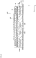
- Fig. 15 is a cross-sectional view of an stretchable wiring board 10C according to the third embodiment.
- the present embodiment is different from the second embodiment in that the stretchable wiring board 10C includes the seam tape 90, but the other configuration is the same as the second embodiment.
- the seam tape 90 which is a difference from the second embodiment in the third embodiment, will be described, and the same reference numerals are given to the same components as those in the second embodiment, and the description thereof will be omitted.
- the "seam tape 90" in this embodiment corresponds to the "second stretchable substrate" in the present invention.
- the difference between the stretchable board 10C and the stretchable board 10B in the second embodiment is that the seam tape 90 is affixed on the overcoat layer 70. This seam tape 90 is affixed to a position corresponding to the wiring portion 61.
- the seam tape 90 has stretchability, and there is no particular limitation on the seam tape 90, but a seam tape provided with a hot-melt on a main surface of a film composed of a urethane-based elastomer can be used. Further, seam tape 90 is softer than the second reinforcing member 40B (in other words, the second reinforcing member 40B is harder than the seam tape 90), the Young's modulus E s of the seam tape 90 is smaller than the Young's modulus E RB of the second reinforcing member (E s ⁇ E RB ). Also, the rupture elongation B s of seam tape 90 is greater than the rupture elongation B h of hot-melt layer 30A (B s >B h ).
- the handling performance of the stretchable wiring board 10C can be improved in the same manner as in the second embodiment described above.
- the rigidity of the portion where the wiring portion 61 is formed of the stretchable wiring board 10C is further improved by the seam tape 90, the handling property is further improved.
- the "second stretchable substrate” is not limited to only the seam tape 90.
- various resin materials can be used, and in particular, it is preferable that the resin material has a waterproof property.
- “seam tape” is exemplified as a resin material having waterproofness.
- the method of manufacturing the stretchable wiring pattern board 10C of the present embodiment is basically the same as the method of manufacturing the stretchable wiring board 10B of the second embodiment, but differs from the second embodiment in that it has difference of attaching the seam tape 90 after the step S8 of Fig. 13 .
- a hot-melt included in the seam tape 90 may be affixed onto the overcoat layer 70 by a thermal laminator or the like.
- the stretchable wiring board 10C is manufactured.
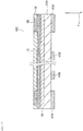
- Fig. 16 is a cross-sectional view of an stretchable wiring board 10D according to the fourth embodiment of the present invention.
- the first stretchable substrate of the stretchable wiring board 10D is an elastomer layer 30B rather than a hot-melt layer 30A, and is different from the second embodiment in that the fabric 20 is not attached, but the other configurations are the same as those of the second embodiment.
- the "elastomer layer 30B" in this embodiment corresponds to the "first stretchable substrate" in the present invention.
- the elastomer layer 30B is formed at the lowermost portion of the stretchable wiring board 10D, and has substantially the same planar shape as the primer layer 50, the conductor portion 60, and the overcoat layer 70.
- the first and second reinforcing members 40A and 40B are buried in the elastomer layer 30B, and the primer layer 50 is formed on the elastomer layer 30B.
- the fabric 20 of the first embodiment is not affixed to the elastomer layer 30B.
- a material constituting the elastomer layer 30B for example, natural rubber, styrene butadiene rubber, butadiene rubber, chloroprene rubber, butyl rubber, nitrile rubber, ethylene propylene rubber, acrylic rubber, urethane rubber, silicone rubber, or fluorine rubber can be used. Note that other elastomeric materials may be used.
- the Young's modulus E E of the elastomer layer 30B is preferably 0.1 MPa to 35MPa. It is preferable that the maximum elongation LE E of the elastomer layer 30B is 5 to 50%.
- the rupture elongation B E of the elastomer layers 30B is preferably 50% or more.
- the thickness T E of the elastomeric layer 30B is preferably 20 ⁇ m to 300 ⁇ m.
- the handling performance of the stretchable wiring board 10D can be improved in the same manner as in the second embodiment described above.
- the stretchable wiring board 10D of the fourth embodiment can be manufactured by printing the primer layer on an elastomer substrate, printing the conductor portion, and printing the overcoat layer.
- Fig. 17 is a cross-sectional view of an stretchable wiring board 10E according to the fifth embodiment of the present invention.
- the present embodiment differs from the fourth embodiment in that the first and second reinforcing members 40A and 40B are formed on the lowermost surface of the stretchable wiring board 10E, but the other configurations are the same as those of the fourth embodiment.
- the same reference numerals are given to the same components as those in the third embodiment, and description thereof will be omitted.
- the first and second reinforcing members 40A and 40B are affixed to the lower surface of the elastomer layer 30B. That is, the first and second reinforcing members 40A and 40B are not buried in the elastomer layer 30B, the first and second reinforcing members 40A and 40B are spaced apart from the primer layer 50, the elastomer layer 30B is interposed between the primer layer 50 and the first and second reinforcing members 40A and 40B.
- the handling performance of the stretchable wiring board 10E can be improved in the same manner as in the second embodiment described above.
- the stretchable wiring board 10E in this fifth embodiment can basically be manufactured by the same manufacturing method as the manufacturing method of the stretchable wiring board 10D in the fourth embodiment, except that the first and second reinforcing members 40A and 40B are affixed to the elastomer layer 30B after the elastomer layer 30B is formed.
- the manufacturing method of the stretchable wiring board 10A is not limited to only the first embodiment described above, and the order of performing the second to seventh steps is not limited to only the order in the embodiment described above.
- a third step may be performed prior to the second step. That is, before the overcoat layer 70 is formed, the connection portion 62 may be formed on the release film 80, then the overcoat layer 70 may be formed, and then the wiring portion 61 may be formed.
- the first and second reinforcing members 40A and 40B may be affixed to the overcoat layer 70.
- the primer layer 50 may not be provided. That is, in the above embodiment, the conductor portion 60 is indirectly provided on the hot-melt layer 30A or the elastomer layer 30B via the primer layer 50, but the conductor portion 60 may be directly provided on the first stretchable substrate, and "provided on the first stretchable substrate" in the present embodiment means "provided indirectly or directly on the first stretchable substrate".
- the method of manufacturing the stretchable wiring board 10B is not limited to only the above-described embodiment, and the order of performing steps 2 to 8 is not limited to only the order in the above-described second embodiment (refer to Fig. 12 ).
- the connection portion 62 may be formed on the release film 80, then the overcoat layer 70 may be formed, and then the wiring portion 61 may be formed.
- a part of the connection portion 62 may be formed on the release film 80, after which the overcoat layer 70 is formed, and then the remaining portion of the connection portion 62 and the wiring portion 61 may be formed simultaneously.
- a manufacturing method can be used when a part of the connection portion 62 includes conductive particles of a different type from the wiring portion 61, and the remaining part of the connection portion 62 includes conductive particles of the same type as the wiring portion 61. More specifically, such a manufacturing method can be used in the case where a part of the connection portion 62 contains carbon as the conductive particles and the remaining portion of the connection portion 62 and the wiring portion 61 contain silver as the conductive particles.
Landscapes
- Engineering & Computer Science (AREA)
- Microelectronics & Electronic Packaging (AREA)
- Manufacturing & Machinery (AREA)
- Structure Of Printed Boards (AREA)
- Laminated Bodies (AREA)
- Non-Metallic Protective Coatings For Printed Circuits (AREA)
Applications Claiming Priority (3)
| Application Number | Priority Date | Filing Date | Title |
|---|---|---|---|
| JP2018050529A JP7144163B2 (ja) | 2018-03-19 | 2018-03-19 | 伸縮性配線板 |
| JP2018050527A JP2019165048A (ja) | 2018-03-19 | 2018-03-19 | 伸縮性配線板及び伸縮性配線板の製造方法 |
| PCT/JP2019/011425 WO2019181931A1 (ja) | 2018-03-19 | 2019-03-19 | 伸縮性配線板及び伸縮性配線板の製造方法 |
Publications (2)
| Publication Number | Publication Date |
|---|---|
| EP3771299A1 true EP3771299A1 (de) | 2021-01-27 |
| EP3771299A4 EP3771299A4 (de) | 2021-12-01 |
Family
ID=67986461
Family Applications (1)
| Application Number | Title | Priority Date | Filing Date |
|---|---|---|---|
| EP19772152.5A Pending EP3771299A4 (de) | 2018-03-19 | 2019-03-19 | Dehnbare leiterplatte und verfahren zur herstellung einer dehnbaren leiterplatte |
Country Status (5)
| Country | Link |
|---|---|
| US (1) | US11337304B2 (de) |
| EP (1) | EP3771299A4 (de) |
| CN (1) | CN111418271B (de) |
| TW (1) | TWI703959B (de) |
| WO (1) | WO2019181931A1 (de) |
Families Citing this family (7)
| Publication number | Priority date | Publication date | Assignee | Title |
|---|---|---|---|---|
| CN110740570A (zh) * | 2018-07-20 | 2020-01-31 | 京东方科技集团股份有限公司 | 柔性线路板、灯条、光源和显示装置 |
| JP2021053169A (ja) * | 2019-09-30 | 2021-04-08 | 住友理工株式会社 | 圧電センサおよび生体情報取得用衣服 |
| US12284767B2 (en) * | 2019-11-25 | 2025-04-22 | Fujikura Ltd. | Method for manufacturing wiring board, wiring board, method for manufacturing molded object, molded object |
| CN114271034B (zh) | 2020-05-21 | 2024-08-30 | 株式会社村田制作所 | 伸缩性布线基板 |
| EP4217192A4 (de) | 2020-09-22 | 2024-10-30 | Burlington Industries LLC | Schutzkleidung und nahtband dafür |
| JP7634555B2 (ja) * | 2020-11-16 | 2025-02-21 | 株式会社フジクラ | 配線板及び配線板の製造方法 |
| WO2025173748A1 (ja) * | 2024-02-14 | 2025-08-21 | 株式会社村田製作所 | 伸縮性デバイス |
Family Cites Families (13)
| Publication number | Priority date | Publication date | Assignee | Title |
|---|---|---|---|---|
| JP2014023613A (ja) | 2012-07-25 | 2014-02-06 | Maruhon Industry Co Ltd | パチンコ機 |
| JP6323982B2 (ja) | 2013-02-26 | 2018-05-16 | 株式会社フジクラ | 伸縮性基板を備える電子部品及びその製造方法 |
| JP6574576B2 (ja) * | 2015-02-02 | 2019-09-11 | 株式会社フジクラ | 伸縮性配線基板 |
| JP6506653B2 (ja) | 2015-07-30 | 2019-04-24 | 日本メクトロン株式会社 | 伸縮性配線基板 |
| US20190045627A1 (en) * | 2015-09-17 | 2019-02-07 | Sekisui Polymatech Co., Ltd. | Elastic Wiring Member |
| JP6676373B2 (ja) * | 2015-10-01 | 2020-04-08 | 日本メクトロン株式会社 | 伸縮性配線基板および伸縮性配線基板の製造方法 |
| JP6741026B2 (ja) * | 2016-01-13 | 2020-08-19 | 東洋紡株式会社 | 伸縮性導体組成物、伸縮性導体形成用ペースト、伸縮性導体組成物からなる配線を有する衣服、およびその製造方法 |
| KR20180114114A (ko) * | 2016-02-12 | 2018-10-17 | 도요보 가부시키가이샤 | 의복형 전자 기기, 및 의복형 전자 기기의 제조방법 |
| JP6859760B2 (ja) * | 2016-03-08 | 2021-04-14 | 東洋紡株式会社 | 伸縮性導体形成用ペースト、伸縮性導体シートおよび生体情報計測用プローブ |
| EP3428220A4 (de) * | 2016-03-09 | 2020-02-26 | Toyobo Co., Ltd. | Elastische leiterfolie und paste zur formung einer elastischen leiterfolie |
| CN108778011B (zh) * | 2016-03-16 | 2021-02-12 | 东洋纺株式会社 | 可穿戴智能装置 |
| JP6799248B2 (ja) | 2016-09-28 | 2020-12-16 | 澁谷工業株式会社 | 細胞シートの切断方法 |
| JP6723130B2 (ja) | 2016-09-28 | 2020-07-15 | デンカ株式会社 | 防草材及びそれの使用方法 |
-
2019
- 2019-03-19 TW TW108109285A patent/TWI703959B/zh active
- 2019-03-19 US US16/979,248 patent/US11337304B2/en active Active
- 2019-03-19 WO PCT/JP2019/011425 patent/WO2019181931A1/ja not_active Ceased
- 2019-03-19 EP EP19772152.5A patent/EP3771299A4/de active Pending
- 2019-03-19 CN CN201980006161.2A patent/CN111418271B/zh active Active
Also Published As
| Publication number | Publication date |
|---|---|
| WO2019181931A1 (ja) | 2019-09-26 |
| US20210059046A1 (en) | 2021-02-25 |
| CN111418271B (zh) | 2022-11-01 |
| CN111418271A (zh) | 2020-07-14 |
| TW201944961A (zh) | 2019-12-01 |
| US11337304B2 (en) | 2022-05-17 |
| EP3771299A4 (de) | 2021-12-01 |
| TWI703959B (zh) | 2020-09-11 |
Similar Documents
| Publication | Publication Date | Title |
|---|---|---|
| EP3771299A1 (de) | Dehnbare leiterplatte und verfahren zur herstellung einer dehnbaren leiterplatte | |
| KR102625030B1 (ko) | 분리형 구조체 및 분리형 센서 구조체 | |
| US9961766B2 (en) | Stretchable circuit board and method for manufacturing stretchable circuit board | |
| JP2019165048A (ja) | 伸縮性配線板及び伸縮性配線板の製造方法 | |
| EP1887497B1 (de) | RFID-Etikett | |
| CN101159034A (zh) | Rfid标签 | |
| US10908685B2 (en) | Hand-wearable device and manufacturing method therefor | |
| TWI588793B (zh) | 可撓性運算織物,其形成方法及包含此可撓性運算織物的衣服 | |
| CN108141960B (zh) | 应力缓和基板及纺织型器件 | |
| EP2058752A1 (de) | RFID-Etikett | |
| US11882653B2 (en) | Continuous interconnects between heterogeneous materials | |
| JP7144163B2 (ja) | 伸縮性配線板 | |
| EP3544392B1 (de) | Elektronische vorrichtung und verfahren zur herstellung davon | |
| KR101237911B1 (ko) | 직물형 압력센서 패키지 제조방법 | |
| US11490527B2 (en) | Method for providing electrical connections and apparatus comprising electrical connections | |
| EP3822328A1 (de) | Längliches elastisches nahtband mit elektrischem leiter | |
| US9705262B2 (en) | Electronic subassembly for apparel | |
| US12588139B2 (en) | Wiring board and method for manufacturing wiring board | |
| US11683885B2 (en) | Sheet-like device and manufacturing method of the same | |
| CN217721599U (zh) | 一种穿戴显示屏的驱动fpc与触控fpc一体化结构 |
Legal Events
| Date | Code | Title | Description |
|---|---|---|---|
| STAA | Information on the status of an ep patent application or granted ep patent |
Free format text: STATUS: THE INTERNATIONAL PUBLICATION HAS BEEN MADE |
|
| PUAI | Public reference made under article 153(3) epc to a published international application that has entered the european phase |
Free format text: ORIGINAL CODE: 0009012 |
|
| STAA | Information on the status of an ep patent application or granted ep patent |
Free format text: STATUS: REQUEST FOR EXAMINATION WAS MADE |
|
| 17P | Request for examination filed |
Effective date: 20200811 |
|
| AK | Designated contracting states |
Kind code of ref document: A1 Designated state(s): AL AT BE BG CH CY CZ DE DK EE ES FI FR GB GR HR HU IE IS IT LI LT LU LV MC MK MT NL NO PL PT RO RS SE SI SK SM TR |
|
| AX | Request for extension of the european patent |
Extension state: BA ME |
|
| DAV | Request for validation of the european patent (deleted) | ||
| DAX | Request for extension of the european patent (deleted) | ||
| A4 | Supplementary search report drawn up and despatched |
Effective date: 20211102 |
|
| RIC1 | Information provided on ipc code assigned before grant |
Ipc: H05K 3/28 20060101ALI20211026BHEP Ipc: B32B 7/025 20190101ALI20211026BHEP Ipc: H05K 1/02 20060101AFI20211026BHEP |
|
| STAA | Information on the status of an ep patent application or granted ep patent |
Free format text: STATUS: EXAMINATION IS IN PROGRESS |
|
| 17Q | First examination report despatched |
Effective date: 20240911 |