EP3771987B1 - Elektronische vorrichtung zur verhinderung der beschädigung von usb-vorrichtungen und betriebsverfahren dafür - Google Patents
Elektronische vorrichtung zur verhinderung der beschädigung von usb-vorrichtungen und betriebsverfahren dafür Download PDFInfo
- Publication number
- EP3771987B1 EP3771987B1 EP20188347.7A EP20188347A EP3771987B1 EP 3771987 B1 EP3771987 B1 EP 3771987B1 EP 20188347 A EP20188347 A EP 20188347A EP 3771987 B1 EP3771987 B1 EP 3771987B1
- Authority
- EP
- European Patent Office
- Prior art keywords
- charging
- usb
- voltage
- electronic device
- designated
- Prior art date
- Legal status (The legal status is an assumption and is not a legal conclusion. Google has not performed a legal analysis and makes no representation as to the accuracy of the status listed.)
- Active
Links
Images




Classifications
-
- G—PHYSICS
- G06—COMPUTING OR CALCULATING; COUNTING
- G06F—ELECTRIC DIGITAL DATA PROCESSING
- G06F13/00—Interconnection of, or transfer of information or other signals between, memories, input/output devices or central processing units
- G06F13/38—Information transfer, e.g. on bus
- G06F13/42—Bus transfer protocol, e.g. handshake; Synchronisation
- G06F13/4282—Bus transfer protocol, e.g. handshake; Synchronisation on a serial bus, e.g. I2C bus, SPI bus
- G06F13/4295—Bus transfer protocol, e.g. handshake; Synchronisation on a serial bus, e.g. I2C bus, SPI bus using an embedded synchronisation
-
- H—ELECTRICITY
- H01—ELECTRIC ELEMENTS
- H01R—ELECTRICALLY-CONDUCTIVE CONNECTIONS; STRUCTURAL ASSOCIATIONS OF A PLURALITY OF MUTUALLY-INSULATED ELECTRICAL CONNECTING ELEMENTS; COUPLING DEVICES; CURRENT COLLECTORS
- H01R13/00—Details of coupling devices of the kinds covered by groups H01R12/70 or H01R24/00 - H01R33/00
- H01R13/66—Structural association with built-in electrical component
- H01R13/665—Structural association with built-in electrical component with built-in electronic circuit
- H01R13/6675—Structural association with built-in electrical component with built-in electronic circuit with built-in power supply
-
- H—ELECTRICITY
- H01—ELECTRIC ELEMENTS
- H01R—ELECTRICALLY-CONDUCTIVE CONNECTIONS; STRUCTURAL ASSOCIATIONS OF A PLURALITY OF MUTUALLY-INSULATED ELECTRICAL CONNECTING ELEMENTS; COUPLING DEVICES; CURRENT COLLECTORS
- H01R13/00—Details of coupling devices of the kinds covered by groups H01R12/70 or H01R24/00 - H01R33/00
- H01R13/66—Structural association with built-in electrical component
- H01R13/665—Structural association with built-in electrical component with built-in electronic circuit
-
- G—PHYSICS
- G06—COMPUTING OR CALCULATING; COUNTING
- G06F—ELECTRIC DIGITAL DATA PROCESSING
- G06F1/00—Details not covered by groups G06F3/00 - G06F13/00 and G06F21/00
- G06F1/26—Power supply means, e.g. regulation thereof
- G06F1/266—Arrangements to supply power to external peripherals either directly from the computer or under computer control, e.g. supply of power through the communication port, computer controlled power-strips
-
- G—PHYSICS
- G06—COMPUTING OR CALCULATING; COUNTING
- G06F—ELECTRIC DIGITAL DATA PROCESSING
- G06F1/00—Details not covered by groups G06F3/00 - G06F13/00 and G06F21/00
- G06F1/26—Power supply means, e.g. regulation thereof
- G06F1/28—Supervision thereof, e.g. detecting power-supply failure by out of limits supervision
-
- G—PHYSICS
- G06—COMPUTING OR CALCULATING; COUNTING
- G06F—ELECTRIC DIGITAL DATA PROCESSING
- G06F13/00—Interconnection of, or transfer of information or other signals between, memories, input/output devices or central processing units
- G06F13/38—Information transfer, e.g. on bus
- G06F13/40—Bus structure
- G06F13/4004—Coupling between buses
-
- G—PHYSICS
- G06—COMPUTING OR CALCULATING; COUNTING
- G06F—ELECTRIC DIGITAL DATA PROCESSING
- G06F13/00—Interconnection of, or transfer of information or other signals between, memories, input/output devices or central processing units
- G06F13/38—Information transfer, e.g. on bus
- G06F13/42—Bus transfer protocol, e.g. handshake; Synchronisation
- G06F13/4282—Bus transfer protocol, e.g. handshake; Synchronisation on a serial bus, e.g. I2C bus, SPI bus
-
- H—ELECTRICITY
- H01—ELECTRIC ELEMENTS
- H01R—ELECTRICALLY-CONDUCTIVE CONNECTIONS; STRUCTURAL ASSOCIATIONS OF A PLURALITY OF MUTUALLY-INSULATED ELECTRICAL CONNECTING ELEMENTS; COUPLING DEVICES; CURRENT COLLECTORS
- H01R13/00—Details of coupling devices of the kinds covered by groups H01R12/70 or H01R24/00 - H01R33/00
- H01R13/66—Structural association with built-in electrical component
- H01R13/665—Structural association with built-in electrical component with built-in electronic circuit
- H01R13/6666—Structural association with built-in electrical component with built-in electronic circuit with built-in overvoltage protection
-
- H—ELECTRICITY
- H01—ELECTRIC ELEMENTS
- H01R—ELECTRICALLY-CONDUCTIVE CONNECTIONS; STRUCTURAL ASSOCIATIONS OF A PLURALITY OF MUTUALLY-INSULATED ELECTRICAL CONNECTING ELEMENTS; COUPLING DEVICES; CURRENT COLLECTORS
- H01R13/00—Details of coupling devices of the kinds covered by groups H01R12/70 or H01R24/00 - H01R33/00
- H01R13/66—Structural association with built-in electrical component
- H01R13/665—Structural association with built-in electrical component with built-in electronic circuit
- H01R13/6683—Structural association with built-in electrical component with built-in electronic circuit with built-in sensor
-
- H—ELECTRICITY
- H01—ELECTRIC ELEMENTS
- H01R—ELECTRICALLY-CONDUCTIVE CONNECTIONS; STRUCTURAL ASSOCIATIONS OF A PLURALITY OF MUTUALLY-INSULATED ELECTRICAL CONNECTING ELEMENTS; COUPLING DEVICES; CURRENT COLLECTORS
- H01R24/00—Two-part coupling devices, or either of their cooperating parts, characterised by their overall structure
- H01R24/60—Contacts spaced along planar side wall transverse to longitudinal axis of engagement
-
- H—ELECTRICITY
- H02—GENERATION; CONVERSION OR DISTRIBUTION OF ELECTRIC POWER
- H02J—ELECTRIC POWER NETWORKS; CIRCUIT ARRANGEMENTS OR SYSTEMS FOR SUPPLYING OR DISTRIBUTING ELECTRIC POWER; SYSTEMS FOR STORING ELECTRIC ENERGY
- H02J7/00—Circuit arrangements for charging or discharging batteries or for supplying loads from batteries
- H02J7/60—Circuit arrangements for charging or discharging batteries or for supplying loads from batteries including safety or protection arrangements
- H02J7/65—Circuit arrangements for charging or discharging batteries or for supplying loads from batteries including safety or protection arrangements against overtemperature
-
- G—PHYSICS
- G06—COMPUTING OR CALCULATING; COUNTING
- G06F—ELECTRIC DIGITAL DATA PROCESSING
- G06F2213/00—Indexing scheme relating to interconnection of, or transfer of information or other signals between, memories, input/output devices or central processing units
- G06F2213/0042—Universal serial bus [USB]
-
- H—ELECTRICITY
- H02—GENERATION; CONVERSION OR DISTRIBUTION OF ELECTRIC POWER
- H02J—ELECTRIC POWER NETWORKS; CIRCUIT ARRANGEMENTS OR SYSTEMS FOR SUPPLYING OR DISTRIBUTING ELECTRIC POWER; SYSTEMS FOR STORING ELECTRIC ENERGY
- H02J2207/00—Details of circuit arrangements for charging or discharging batteries or supplying loads from batteries
- H02J2207/30—Charge provided using DC bus or data bus of a computer
Definitions
- the disclosure relates to a device and an operating method for preventing damage of a universal serial bus (USB) device connected to an electronic device.
- USB universal serial bus
- Electronic devices have been provided in various forms, such as a smart phone, a tablet personal computer (PC), and a personal digital assistant (PDA). Electronic devices have also been developed in a form that can be worn by a user so as to improve portability and accessibility of the user.
- a smart phone such as a smart phone, a tablet personal computer (PC), and a personal digital assistant (PDA).
- PDA personal digital assistant
- USB Type-C interface a Type-C standard
- various USB devices supporting the USB Type-C interface have been developed.
- earphones supporting a USB Type-C interface have been provided instead of existing 3.5-Pi earphones.
- US 2010/0070659 A1 discloses method and system for operating and/or charging a battery powered USB device based on a USB port type, wherein: a port type detection module in the multi-function IC may determine whether the USD device is attached to a standard host port or a charging port; a power source in the power management IC may be enabled upon attachment of the USB device to a USB port and disabled subsequent to determination of port type; and one or more portions and/or functions of the power management IC may be configured based on the determined port type.
- An electronic device may be simultaneously connected to a plurality of USB devices supporting a USB Type-C interface, using a USB Type-C dual gender.
- the electronic device may be connected to a charging device supporting fast charging and USB Type-C earphones, using a USB Type-C dual gender.
- a high voltage which has been boosted to 9V for fast charging in a charging device, flows into a USB bus voltage (VBUS) line of the USB Type-C earphones, and thus may cause heat generation in the earphones. Heat generation of the earphone may lead to damage of the earphone.
- VBUS USB bus voltage
- an aspect of the disclosure is to provide a device and a method for preventing damage of a USB device in an electronic device.
- the invention is defined according to the apparatus of claim 1 and the method of claim 10.
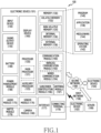
- FIG. 1 is a block diagram illustrating an electronic device 101 in a network environment 100 according to an embodiment of the disclosure.
- the electronic device 101 in the network environment 100 may communicate with an electronic device 102 via a first network 198 (e.g., a short-range wireless communication network), or an electronic device 104 or a server 108 via a second network 199 (e.g., a long-range wireless communication network).
- a first network 198 e.g., a short-range wireless communication network
- an electronic device 104 or a server 108 via a second network 199 (e.g., a long-range wireless communication network).
- the electronic device 101 may communicate with the electronic device 104 via the server 108.
- the electronic device 101 may include a processor 120, memory 130, an input device 150, a sound output device 155, a display device 160, an audio module 170, a sensor module 176, an interface 177, a haptic module 179, a camera module 180, a power management module 188, a battery 189, a communication module 190, a subscriber identification module (SIM) 196, or an antenna module 197.
- at least one (e.g., the display device 160 or the camera module 180) of the components may be omitted from the electronic device 101, or one or more other components may be added in the electronic device 101.
- some of the components may be implemented as single integrated circuitry.
- the sensor module 176 e.g., a fingerprint sensor, an iris sensor, or an illuminance sensor
- the display device 160 e.g., a display
- an haptic module 179 e.g., a camera module 180
- a power management module 188 e.g., the display
- the processor 120 may execute, for example, software (e.g., a program 140) to control at least one other component (e.g., a hardware or software component) of the electronic device 101 coupled with the processor 120, and may perform various data processing or computation. According to one embodiment, as at least part of the data processing or computation, the processor 120 may load a command or data received from another component (e.g., the sensor module 176 or the communication module 190) in volatile memory 132, process the command or the data stored in the volatile memory 132, and store resulting data in non-volatile memory 134.
- software e.g., a program 140
- the processor 120 may load a command or data received from another component (e.g., the sensor module 176 or the communication module 190) in volatile memory 132, process the command or the data stored in the volatile memory 132, and store resulting data in non-volatile memory 134.
- the processor 120 may include a main processor 121 (e.g., a central processing unit (CPU) or an application processor (AP)), and an auxiliary processor 123 (e.g., a graphics processing unit (GPU), an image signal processor (ISP), a sensor hub processor, or a communication processor (CP)) that is operable independently from, or in conjunction with, the main processor 121.
- auxiliary processor 123 may be adapted to consume less power than the main processor 121, or to be specific to a specified function.
- the auxiliary processor 123 may be implemented as separate from, or as part of the main processor 121.
- the auxiliary processor 123 may control at least some of functions or states related to at least one component (e.g., the display device 160, the sensor module 176, or the communication module 190) among the components of the electronic device 101, instead of the main processor 121 while the main processor 121 is in an inactive (e.g., sleep) state, or together with the main processor 121 while the main processor 121 is in an active state (e.g., executing an application).
- the auxiliary processor 123 e.g., an image signal processor or a communication processor
- the memory 130 may store various data used by at least one component (e.g., the processor 120 or the sensor module 176) of the electronic device 101.
- the various data may include, for example, software (e.g., the program 140) and input data or output data for a command related thereto.
- the memory 130 may include the volatile memory 132 or the non-volatile memory 134.
- the program 140 may be stored in the memory 130 as software, and may include, for example, an operating system (OS) 142, middleware 144, or an application 146.
- OS operating system
- middleware middleware
- application application
- the input device 150 may receive a command or data to be used by other component (e.g., the processor 120) of the electronic device 101, from the outside (e.g., a user) of the electronic device 101.
- the input device 150 may include, for example, a microphone, a mouse, a keyboard, or a digital pen (e.g., a stylus pen).
- the sound output device 155 may output sound signals to the outside of the electronic device 101.
- the sound output device 155 may include, for example, a speaker or a receiver.
- the speaker may be used for general purposes, such as playing multimedia or playing record, and the receiver may be used for incoming calls. According to an embodiment, the receiver may be implemented as separate from, or as part of the speaker.
- the display device 160 may visually provide information to the outside (e.g., a user) of the electronic device 101.
- the display device 160 may include, for example, a display, a hologram device, or a projector and control circuitry to control a corresponding one of the display, hologram device, and projector.
- the display device 160 may include touch circuitry adapted to detect a touch, or sensor circuitry (e.g., a pressure sensor) adapted to measure the intensity of force incurred by the touch.
- the audio module 170 may convert a sound into an electrical signal and vice versa. According to an embodiment, the audio module 170 may obtain the sound via the input device 150, or output the sound via the sound output device 155 or a headphone of an external electronic device (e.g., an electronic device 102) directly (e.g., wiredly) or wirelessly coupled with the electronic device 101.
- an external electronic device e.g., an electronic device 102
- directly e.g., wiredly
- wirelessly e.g., wirelessly
- the sensor module 176 may detect an operational state (e.g., power or temperature) of the electronic device 101 or an environmental state (e.g., a state of a user) external to the electronic device 101, and then generate an electrical signal or data value corresponding to the detected state.
- the sensor module 176 may include, for example, a gesture sensor, a gyro sensor, an atmospheric pressure sensor, a magnetic sensor, an acceleration sensor, a grip sensor, a proximity sensor, a color sensor, an infrared (IR) sensor, a biometric sensor, a temperature sensor, a humidity sensor, or an illuminance sensor.
- the interface 177 may support one or more specified protocols to be used for the electronic device 101 to be coupled with the external electronic device (e.g., the electronic device 102) directly (e.g., wiredly) or wirelessly.
- the interface 177 may include, for example, a high definition multimedia interface (HDMI), a universal serial bus (USB) interface, a secure digital (SD) card interface, or an audio interface.
- HDMI high definition multimedia interface
- USB universal serial bus
- SD secure digital
- a connecting terminal 178 may include a connector via which the electronic device 101 may be physically connected with the external electronic device (e.g., the electronic device 102).
- the connecting terminal 178 may include, for example, a HDMI connector, a USB connector, a SD card connector, or an audio connector (e.g., a headphone connector).
- the haptic module 179 may convert an electrical signal into a mechanical stimulus (e.g., a vibration or a movement) or electrical stimulus which may be recognized by a user via his tactile sensation or kinesthetic sensation.
- the haptic module 179 may include, for example, a motor, a piezoelectric element, or an electric stimulator.
- the camera module 180 may capture a still image or moving images.
- the camera module 180 may include one or more lenses, image sensors, image signal processors, or flashes.
- the power management module 188 may manage power supplied to the electronic device 101.
- the power management module 188 may be implemented as at least part of, for example, a power management integrated circuit (PMIC).
- PMIC power management integrated circuit
- the battery 189 may supply power to at least one component of the electronic device 101.
- the battery 189 may include, for example, a primary cell which is not rechargeable, a secondary cell which is rechargeable, or a fuel cell.
- the communication module 190 may support establishing a direct (e.g., wired) communication channel or a wireless communication channel between the electronic device 101 and the external electronic device (e.g., the electronic device 102, the electronic device 104, or the server 108) and performing communication via the established communication channel.
- the communication module 190 may include one or more communication processors that are operable independently from the processor 120 (e.g., the application processor (AP)) and supports a direct (e.g., wired) communication or a wireless communication.
- AP application processor
- the communication module 190 may include a wireless communication module 192 (e.g., a cellular communication module, a short-range wireless communication module, or a global navigation satellite system (GNSS) communication module) or a wired communication module 194 (e.g., a local area network (LAN) communication module or a power line communication (PLC) module).
- a wireless communication module 192 e.g., a cellular communication module, a short-range wireless communication module, or a global navigation satellite system (GNSS) communication module
- GNSS global navigation satellite system
- wired communication module 194 e.g., a local area network (LAN) communication module or a power line communication (PLC) module.
- LAN local area network
- PLC power line communication
- a corresponding one of these communication modules may communicate with the external electronic device via the first network 198 (e.g., a short-range communication network, such as Bluetooth TM , wireless-fidelity (Wi-Fi) direct, or infrared data association (IrDA)) or the second network 199 (e.g., a long-range communication network, such as a cellular network, the Internet, or a computer network (e.g., LAN or wide area network (WAN)).
- the first network 198 e.g., a short-range communication network, such as Bluetooth TM , wireless-fidelity (Wi-Fi) direct, or infrared data association (IrDA)
- the second network 199 e.g., a long-range communication network, such as a cellular network, the Internet, or a computer network (e.g., LAN or wide area network (WAN)
- These various types of communication modules may be implemented as a single component (e.g., a single chip), or may be implemented as multi
- the wireless communication module 192 may identify and authenticate the electronic device 101 in a communication network, such as the first network 198 or the second network 199, using subscriber information (e.g., international mobile subscriber identity (IMSI)) stored in the subscriber identification module 196.
- subscriber information e.g., international mobile subscriber identity (IMSI)
- the antenna module 197 may transmit or receive a signal or power to or from the outside (e.g., the external electronic device) of the electronic device 101.
- the antenna module 197 may include an antenna including a radiating element composed of a conductive material or a conductive pattern formed in or on a substrate (e.g., printed circuit board (PCB)).
- the antenna module 197 may include a plurality of antennas. In such a case, at least one antenna appropriate for a communication scheme used in the communication network, such as the first network 198 or the second network 199, may be selected, for example, by the communication module 190 (e.g., the wireless communication module 192) from the plurality of antennas.
- the signal or the power may then be transmitted or received between the communication module 190 and the external electronic device via the selected at least one antenna.
- another component e.g., a radio frequency integrated circuit (RFIC)
- RFIC radio frequency integrated circuit
- an inter-peripheral communication scheme e.g., a bus, general purpose input and output (GPIO), serial peripheral interface (SPI), or mobile industry processor interface (MIPI)
- GPIO general purpose input and output
- SPI serial peripheral interface
- MIPI mobile industry processor interface
- commands or data may be transmitted or received between the electronic device 101 and the external electronic device 104 via the server 108 coupled with the second network 199.
- Each of the electronic devices 102 and 104 may be a device of a same type as, or a different type, from the electronic device 101.
- all or some of operations to be executed at the electronic device 101 may be executed at one or more of the external electronic devices 102, 104, or 108. For example, if the electronic device 101 should perform a function or a service automatically, or in response to a request from a user or another device, the electronic device 101, instead of, or in addition to, executing the function or the service, may request the one or more external electronic devices to perform at least part of the function or the service.
- the one or more external electronic devices receiving the request may perform the at least part of the function or the service requested, or an additional function or an additional service related to the request, and transfer an outcome of the performing to the electronic device 101.
- the electronic device 101 may provide the outcome, with or without further processing of the outcome, as at least part of a reply to the request.
- a cloud computing, distributed computing, or client-server computing technology may be used, for example.
- the processor 120 may detect a connection of at least two external devices through a USB connector, using a USB interface.
- the USB connector may be a USB Type-C connector.
- the external device may include at least one of a USB Type-C device and a USB Type-C charging device.
- the USB Type-C device may include at least one of USB Type-C earphones and a USB Type-C memory.
- the example above is exemplary, and the USB Type-C device according to various embodiments will not be limited to such arranged examples.
- the USB connector may be connected to two external devices through a USB Type-C dual gender.
- the processor 120 detects a connection of a USB device and a charging device through a USB dual gender, using a USB interface.
- the processor 120 may determine whether the USB device and the charging device are connected through a USB connector and a USB Type-C dual gender connected to the USB connector, based on at least one of a role change for power, identification information of a USB device that is being connected, and an Rp current level change through a CC pin (e.g., a CC1 pin or a CC2 pin) of the USB connector.
- a CC pin e.g., a CC1 pin or a CC2 pin
- the processor 120 controls a charging voltage output from the charging device in order to prevent the USB device from being burned out due to the charging voltage output from the charging device.
- the processor 120 may determine a charging voltage smaller than or equal to a designated voltage, and request the charging device to provide the determined charging voltage.
- the designated voltage may be configured and/or changed by a designer, and may be configured in consideration of voltages supportable by various USB devices.
- the designated voltage may be configured to be about 5V, for example.
- FIG. 2 is a block diagram 200 of an electronic device 101 which is connected to a PD charging device 251 and a USB device 255 using a USB Type-C dual gender 253 according to an embodiment of the disclosure.
- the electronic device 101 of FIG. 2 may be the electronic device 101 of FIG. 1 .
- the operation of at least some elements of FIG. 2 will be described with reference to FIG. 3 .
- FIG. 3 is a diagram illustrating a pin structure 300 of a USB connector 209 supporting a USB Type-C interface according to an embodiment of the disclosure.
- the electronic device 101 may include a software module 201 and a hardware module 207.
- the software module 201 may include a framework 203 and a kernel 205 for controlling one or more resources of the electronic device 101.
- the framework 203 may provide applications for providing various functions using functions or information provided from one or more resources of the electronic device 101.
- the framework 203 may include, for example, a USB framework 211, a battery service 213, and a USB port manager 215.
- the USB framework 211 may manage a data communication function using the USB connector 209.
- the battery service 213 may provide a function related to battery charging.
- the USB port manager 215 may provide a function related to identification of a connection of an external device and determination of a voltage to be provided from the external device and/or a voltage to be provided thereto.
- the USB framework 211, the battery service 213, and the USB port manager 215 may communicate with a USB driver 221, a charging driver 223, and a power delivery IC (PDIC) driver 225, respectively.
- PDIC power delivery IC
- the kernel 205 may control management (e.g., allocation or retrieval) of one or more system resources (e.g., a process, a memory, or power) of the electronic device 101.
- the kernel 205 may include one or more driver programs for driving other hardware devices of the electronic device 101, for example, the input device 150, the sound output device 155, the display device 160, the audio module 170, the sensor module 176, the interface 177, the haptic module 179, the camera module 180, the power management module 188, the battery 189, the communication module 190, the subscriber identification module 196, or the antenna module 197.
- the kernel 205 may include programs for the USB driver 221, the charging driver 223, and the PDIC driver 225.
- the hardware module 207 may include a USB controller 231, a charging IC 233, and a PDIC chipset 235.
- the USB controller 231 may perform USB data communication using D+/D- pins 301, 302, 303, and 304 of the USB connector 209.
- the USB controller 231 may be included in an application processor (AP).
- the charging IC 233 may receive a charging voltage from a PD charging device 251 which is connected through at least one of the USB connector 209 and the USB Type-C dual gender 253 using V BUS pins 321, 322, 323, and 324 of the USB connector 209, or may provide a voltage to the USB device 255 which is connected to the electronic device 101 through at least one of the USB connector 209 and the USB Type-C dual gender 253.
- the PDIC chipset 235 may perform USB PD communication through CC pins 311 and 312 of the USB connector 209, and may perform a function related to power negotiation with the PD charging device 251 connected through the USB connector 209 and the USB Type-C dual gender 253.
- the PDIC chipset 235 may recognize the resistance of the CC pins 311 and 312 of the USB connector 209.
- the charging IC 233 and the PDIC chipset 235 may be configured by an IF PMIC.
- the PDIC driver 225 may recognize that an external device is connected through at least one of the USB connector 209 and the USB Type-C dual gender 253 connected to the USB connector 209, based on a first resistance Rd (e.g., 5.1 S2) or a second resistance Rp (e.g., 56 ⁇ ) which are recognized by the PDIC chipset 235.
- the PDIC driver 225 may determine a role of the electronic device 101 for power based on the resistance values recognized by the CC pins 311 and 312. For example, if the first resistance is recognized by the CC pins 311 and 312, the PDIC driver 225 may determine the role of the electronic device 101 as a source device (or host device) for supplying power.
- the PDIC driver 225 may determine the role of the electronic device 101 as a sink device (or slave device) for receiving power. According to an embodiment, the PDIC driver 225 may switch the role of the electronic device 101 to the source device based on the resistance value detected by the CC pin and then perform USB data communication through D+/D- pins 301, 302, 303, and 304, so as to determine that a USB device 255, such as USB earphones, has been connected through at least one of the USB connector 209 and the USB Type-C dual gender 253.
- the PDIC driver 225 may determine that the PD charging device 251 is connected through at least one of the USB connector 209 and the USB Type-C dual gender 253.
- the PDIC driver 225 may determine that a detach event occurs if the recognized resistance is changed from the first resistance value to another resistance value.
- the PDIC driver 225 may determine whether the second resistance is recognized by the CC pins 311 and 312 within a designated time (e.g., about 320 ms) from a time point at which the detach event occurs. If the second resistance is recognized by the CC pins 311 and 312 within a designated time from the time point where the detach event occurs the PDIC driver 225 may determine that, in addition to the state where the USB device 255 has been connected to the electronic device 101 through the USB connector 209 and the USB Type-C dual gender 253, the PD charging device 251 also has been connected thereto.
- the PDIC driver 225 may determine (or identify) whether time consumed for switching the role of the electronic device 101 to a sink device for receiving power after the detach event occurs in a state where the role of the electronic device 101 corresponds to a source device for supplying power falls within a designated time. In addition, if time consumed for switching the role of the electronic device 101 from a source device to a sink device after the detach event occurs falls within a designated time, the PDIC driver 225 may determine that, in addition to the state where the USB device 255 has been connected to the electronic device 101 through the USB connector 209 and the USB Type-C dual gender 253, the PD charging device 251 also has been connected thereto.
- the PDIC driver 225 may acquire identification information of the USB device 255 through the CC pins 311 and 312 and temporarily store the acquired identification information of the USB device 255.
- the information of the USB device 255 may include at least one of business operator identification information (vender ID) and product identification information (product ID).
- the PDIC driver 225 may determine that, in addition to the state where the USB device 255 has been connected to the electronic device 101 through the USB connector 209 and the USB Type-C dual gender 253, the PD charging device 251 also has been connected thereto.
- the PDIC driver 225 may determine the case to be a situation in which charging voltage limitation is required and perform an operation of limiting the charging voltage.
- the operation of limiting the charging voltage may include at least one of an operation of requesting limitation of the charging voltage from the charging driver 223 or an operation of rejecting a request for boosting up the charging voltage from the charging driver 223.
- the PDIC driver 225 may determine the case to be a situation in which charging voltage limitation is required and perform an operation of limiting the charging voltage.
- the PDIC driver 225 may determine that, in addition to the state where the PD charging device 251 has been connected to the electronic device 101, the USB device 255 also has been connected thereto.
- the PDIC driver 225 may determine the case to be a situation in which charging voltage limitation is required and perform an operation of limiting the charging voltage.
- the operation of limiting the charging voltage may include at least one of an operation of requesting limitation of the charging voltage from the charging driver 223 or an operation of rejecting a request for boosting up the charging voltage from the charging driver 223.
- the PDIC driver 225 may transmit the received charging request signal to the PD charging device 251 through the PDIC chipset 235.
- the PDIC driver 225 may compare the charging voltage selected by the charging driver 223 with the designated voltage, and determine whether to transmit the received charging request signal to the PD charging device 251. If the charging voltage selected by the charging driver 223 is smaller than or equal to a designated voltage, the PDIC driver 225 may transmit the received charging request signal to the PD charging device 251 through the PDIC chipset 235. If the charging voltage selected by the charging driver 223 is greater than a designated voltage, the PDIC driver 225 may not transmit the received charging request signal to the PD charging device 251, but transmit, to the PDIC driver 225, a rejection signal with respect to the charging request.
- the charging driver 223 may receive, from the PDIC driver 225, a list indicating charging voltages supportable by the PD charging device 251.
- the charging driver 223 may select a desired charging voltage from the list indicating charging voltages supportable by the PD charging device 251.
- the charging driver 223 may select a charging voltage smaller than or equal to a designated voltage from the list indicating the supportable charging voltages.
- the charging driver 223 may transmit a signal requesting charging to the selected charging voltage to the PDIC driver 225.
- the charging driver 223 may select a charging voltage smaller than or equal to the designated voltage, and may transmit the signal requesting charging to the selected charging voltage to the PDIC driver 225.
- the electronic device 101 includes: a first-type USB connector (e.g., the USB connector 209 of FIG. 2 ) which is connectable with at least one of charging devices (e.g., the PD charging device 251 of FIG. 2 ) and a USB device (e.g., the USB device 255 of FIG. 2 ) through a dual gender (e.g., the USB Type-C dual gender 253 of FIG. 2 ); and a processor (e.g., the processor 120 of FIG.
- a first-type USB connector e.g., the USB connector 209 of FIG. 2
- charging devices e.g., the PD charging device 251 of FIG. 2
- a USB device e.g., the USB device 255 of FIG. 2
- a dual gender e.g., the USB Type-C dual gender 253 of FIG. 2
- a processor e.g., the processor 120 of FIG.
- the processor 120 is configured to: detect a connection of the charging device 251 and the USB device 255 to the electronic device 101 through the USB connector 209; in response to the connection of the charging device 251 and the USB device 255 to the electronic device 101, determine a charging voltage satisfying a designated condition; and request the charging device 251 to provide the determined charging voltage through the USB connector 209.
- the designated condition is configured based on a maximum voltage supportable by the USB device 255.
- the processor 120 may acquire, from the charging device 251, a list including information on charging voltages supportable by the charging device 251.
- the processor may be configured to determine a charging voltage smaller than or equal to the designated voltage among charging voltages supportable by the charging device 251 to be a charging voltage of the electronic device 101.
- the processor 120 may be configured to acquire a list including information on charging voltages supportable by the charging device 251 from the charging device 251.
- the processor 120 may be configured to select one charging voltage from among the charging voltages supportable by the charging device 251, compare the selected charging voltage with a designated voltage, and determine whether to request the charging device to provide the selected charging voltage.
- the processor 120 may be configured to request the charging device to provide the selected charging voltage if the selected charging voltage is smaller than or equal to the designated voltage. In addition, if the selected charging voltage is greater than the designated voltage, the processor 120 may be configured to: reselect another charging voltage from among the charging voltages included in the acquired list; and compare the reselected another charging voltage with the designated voltage, and determine whether to request the charging device to provide the reselected another charging voltage.
- the processor 120 may be configured to determine a current charging voltage received from the charging device 251 with a designated voltage. In addition, if the current charging voltage is greater than the designated voltage, the processor 120 may be configured to select a charging voltage smaller than or equal to the designated voltage from among charging voltages supportable by the charging device 251, and request the charging device 251 to provide the selected charging voltage through the USB connector 209.
- the processor 120 may be configured to detect a connection of the charging device 251 and the USB device 255 to the electronic device 101 through the USB connector 209 based on at least one of change in a role of the electronic device 101 for the power, identification information of the USB device 255, or a current level change recognized through the CC pin of the USB connector 209.
- the processor 120 may detect the occurrence of a detach event, based on a resistance value recognized by the CC pin of the USB connector 209 in a state where the role of the electronic device 101 corresponds to a source device for providing a voltage, and may determine whether the role of the electronic device is switched to a sink device for receiving a voltage within a designated time from a time point at which the detach event occurs.
- the processor 120 may be configured to determine that, in addition to the state where the USB device 255 has been connected to the electronic device 101 through the USB connector 209, the charging device 251 also has been connected thereto.
- the processor 120 may be configured to: detect a connection of the USB device 255 to the USB connector 209 based on a resistance value recognized by the CC pin of the USB connector 209; and acquire identification information of the USB device 255 from the USB device 255 and store the acquired identification information.
- the processor may be configured to determine that, in addition to the state where the USB device 255 has been connected to the electronic device 101 through the USB connector 209, the charging device 251 also has been connected thereto.
- the processor 120 may be configured to determine that, in addition to the state where the charging device 251 has been connected to the electronic device 101 through the USB connector 209, the USB device 255 has also been connected thereto.
- FIG. 4 is a flowchart 400 illustrating an operation of controlling a charging voltage in order to prevent damage of a USB device in an electronic device according to an embodiment of the disclosure.
- the electronic device may be the electronic device 101 of FIG. 1 .
- an electronic device e.g., the processor 120 of FIG. 1 and/or the PDIC driver 225 of FIG. 2
- may detect a connection of a charging device e.g., the PD charging device 251 of FIG. 2
- a USB device e.g., the USB device 255 of FIG. 2
- a USB connector e.g., a connection terminal 178 of FIG. 1 and/or the USB connector 209 of FIG. 2 .
- the processor 120 may determine (or identify) whether the USB device and the charging device are connected to the electronic device 101 through the USB connector 209 (or 178) and a USB Type-C dual gender (e.g., the USB Type-C dual gender 253 of FIG. 2 ) connected to the USB connector 209 (or 178), based on at least one of a role change related to power, identification information of the USB device 255 that is being connected, or an Rp current level change through the CC pins of the USB connector 209 (or 178).
- a USB Type-C dual gender e.g., the USB Type-C dual gender 253 of FIG. 2
- the processor 120 may detect that the role of the electronic device 101 for the power is switched to a sink device from a source device after the detach event occurs, based on the resistance recognized by the CC pins of the USB connector 209 (or 178).
- the processor 120 may measure time consumed while the role of the electronic device 101 for power is changed from the source device to the sink device after a detach event occurs, and if the measured time falls within a designated time, the processor 120 may detect that, in addition to the state where the USB device 255 has been connected to the electronic device 101, the charging device 251 has also been connected thereto.
- the processor 120 may detect that, in addition to the state where the USB device 255 has been connected to the electronic device 101, the charging device 251 also has been connected thereto.
- the processor 120 may detect a change of the Rp current level through the CC pin, and if the change in the Rp current level satisfies a designated condition, the processor 120 may detect that, in addition to the state where the charging device 251 has been connected to the electronic device 101, the USB device 255 also has been connected thereto.
- the electronic device may determine a charging voltage satisfying a designated condition.
- the processor 120 may determine a charging voltage smaller than or equal to a designated voltage.
- the processor 120 may determine a value of the charging voltage to be a value smaller than or equal to a value of a designated voltage in order to protect the USB.
- the designated voltage may be configured by considering the maximum voltage supportable by various USB devices.
- the designated voltage may be configured to be about 5V, for example.
- the electronic device e.g., the processor 120, the PDIC driver 225, and/or the charging driver 223 may request a determined charging voltage from the charging device.
- the processor 120 may transmit a request signal including information about the determined charging voltage to the charging device 251 through the CC pins of the USB connector 209 (or 178).
- FIG. 5 is a flowchart 500 illustrating an operation of limiting selection of a charging voltage by detecting a role change related to power in an electronic device according to the invention.
- the electronic device may be the electronic device 101 of FIG. 1 .
- the operations of FIG. 5 described below may be at least some of the detailed operations of operations 401, 403, and 405 of FIG. 4 .
- an electronic device e.g., the processor 120 of FIG. 1 and/or the PDIC driver 225 of FIG. 2 ) according to the invention determines whether a detach event occurs in a state where a USB device (e.g., the USB device 255 of FIG. 2 ) is connected through a USB connector (e.g., the connection terminal 178 of FIG. 1 and/or the USB connector 209 of FIG. 2 ).
- a USB device e.g., the USB device 255 of FIG. 2
- a USB connector e.g., the connection terminal 178 of FIG. 1 and/or the USB connector 209 of FIG. 2 .
- the PDIC driver 225 may determine the role of the electronic device 101 to be a source device for supplying power to the USB device 255, and may perform USB data communication through the D+/D- pins 301, 302, 303, and 304 to determine that the USB device 255 is connected to the USB connector 209 (or 178). If the resistance recognized by the CC pins of the USB connectors 209 (or 178) is changed from the first resistance value to a different resistance value while the electronic device 101 operates as the source device, the PDIC driver 225 may determine that the detach event occurs.
- a first resistance Rd e.g., 5.1 ⁇
- an electronic device determines whether a sink attach event occurs within a designated time, in operation 503. For example, the PDIC driver 225 may determine whether a second resistance Rp (e.g., 56 ⁇ ) is recognized by the CC pins of the USB connector 209 (or 178) within a designated time (e.g., about 320 ms) from a time point at which the detach event occurs. If the second resistance is recognized, the PDIC driver 225 may change the role of the electronic device 101 to a sink device for receiving power, and may determine that a sink attach event occurs.
- a second resistance Rp e.g., 56 ⁇
- a designated time e.g., about 320 ms
- the electronic device determines that a charging voltage limiting event occurs, in operation 505. For example, if a detach event occurs in a state where the USB device 255 is connected through the USB connector 209 (or 178) and a sink attach event occurs within a designated time from a time point at which the detach event occurs, the PDIC driver 225 may determine that, in addition to the state where the USB device 255 has been connected to the electronic device 101 through the USB connector 209 (or 178) and the USB Type-C dual gender (e.g., USB Type-C dual gender 253 in FIG.
- the electronic device e.g., the processor 120 and/or the PDIC driver 225
- the charging device (the PD charging device 251 of FIG. 2 ) also has been connected thereto.
- the PDIC driver 225 may determine that the charging voltage limitation is required in order to prevent burnout of the USB device 255.
- the PDIC driver 225 may provide notification that the charging voltage needs to be limited to the charging driver 223.
- the PDIC driver 225 may provide notification that the charging voltage needs to be limited to the charging driver 223 by transmitting information indicating that, in addition to the state where the USB device 255 has been connected to the electronic device 101 to the charging driver 223, the charging device 251 also has been connected thereto.
- the PDIC driver 225 may transmit information indicating that a charging voltage limiting event occurs to the charging driver 223.
- the electronic device may select a charging voltage, which is smaller than or equal to a designated voltage, from the list of powers supportable by the charging device.
- the list of powers supportable by the charging device may indicate charging voltages supportable by the charging device.
- the charging driver 223 may receive, from the charging device 251, a list indicating charging voltages supportable by the charging device 251.
- the charging driver 223 may select a charging voltage smaller than or equal to a designated voltage from a list indicating charging voltages supportable by the charging device 251. For example, if 5V and 9V are supportable with reference to the list indicating the charging voltages supportable by the charging device 251, the charging driver 223 may select a charging voltage of 5V equal to the designated voltage (e.g., about 5V).
- the electronic device e.g., the processor 120, the charging driver 223, and/or the PDIC driver 225
- the charging driver 223 may provide a request signal indicating the selected charging voltage to the PDIC driver 225
- the PDIC driver 225 may transmit a request signal indicating the selected charging voltage to the charging device 251 through the PDIC chipset 235.
- FIG. 6A is a graph showing a change in a V BUS voltage level in an electronic device according to the prior art
- FIG. 6B is a graph showing a change in a V BUS voltage level in an electronic device according to an embodiment of the disclosure.
- FIG. 6A illustrates a change in a voltage level measured through the V BUS pin if, in addition to the state where the USB device 255 has been connected to the electronic device according to the prior art through the USB Type-C dual gender, the PD charging device also has been connected thereto.
- FIG. 6B illustrates a change in a voltage level measured through the V BUS pin if, in addition to the state where the USB device 255 has been connected to the electronic device 101 according to various embodiments through the USB Type-C dual gender 253, the PD charging device 251 also has been connected thereto.
- a 5V voltage (indicated by reference numeral 601), which is provided from the electronic device to the USB device, may be applied to the V BUS pin.
- the electronic device may select the maximum charging voltage (for example: 9V) among the charging voltages supportable by the charging device, and may request the charging device to provide the selected charging voltage.
- the boosted voltage of 9V (indicated by reference numeral 605), which is provided from the PD charging device to the electronic device, may be applied to the V BUS pin.
- the boosted voltage of 9V applied to the V BUS pin may be provided to the USB device connected to the electronic device.
- a heat generation phenomenon may occur in the USB device, and thus the USB device may be damaged.
- a USB device for example, the USB device 255 of FIG. 2
- a 5V voltage (indicated by reference numeral 611), which is provided from the electronic device to the USB device 255, may be applied to the V BUS pin.
- the PD charging device for example, the PD charging device 251 of FIG.
- the electronic device may determine the case described above to be a situation in which the charging voltage limitation is required, may select a charging voltage (for example: 5V) smaller than or equal to a designated voltage, and may request the charging device to provide the selected charging voltage. Accordingly, a 5V voltage (indicated by reference numeral 615), which is provided from the PD charging device 251 to the electronic device 101, may be applied to the V BUS pin. The 5V voltage applied to the V BUS pin may be provided to the USB device 255 connected to the electronic device 101. Since the 5V voltage is smaller than or equal to the maximum voltage supportable by the USB device 255, it is possible to prevent a heat generation phenomenon from occurring.
- a charging voltage for example: 5V
- a 5V voltage (indicated by reference numeral 615)
- the 5V voltage applied to the V BUS pin may be provided to the USB device 255 connected to the electronic device 101. Since the 5V voltage is smaller than or equal to the maximum voltage supportable by the USB device 255, it is possible to prevent
- FIG. 7 is a flowchart 700 illustrating an operation of limiting a request for a selected charging voltage by detecting a role change related to power in an electronic device according to an embodiment of the disclosure, not falling under the scope of the claims.
- the electronic device may be the electronic device 101 of FIG. 1 .
- the operations of FIG. 7 described below may be at least some of the detailed operations of operations 401, 403, and 405 of FIG. 4 .
- the electronic device e.g., the processor 120 of FIG. 1 and/or the PDIC driver 225 of FIG. 2
- the electronic device may determine whether a detach event occurs in a state where a USB device (for example, the USB device 255 of FIG. 2 ) is connected through a USB connector (for example, the connection terminal 178 of FIG. 1 and/or the USB connector 209 of FIG. 2 ).
- operation 701 may be the same as operation 501 of FIG. 5 .
- the electronic device e.g., the processor 120 and/or the PDIC driver 225 may determine whether a sink attach event occurs within a designated time, in operation 703.
- operation 703 may be the same as operation 503 of FIG. 5 .
- the electronic device e.g., the processor 120 and/or the PDIC driver 225
- the electronic device may determine that a charging voltage limiting event occurs, in operation 705.
- operation 705 may be at least partially the same as operation 505 of FIG. 5 .
- the PDIC driver 225 may determine that, in addition to the state where the USB device 255 has been connected to the electronic device 101 through the USB connector 209 (or 178) and the USB Type-C dual gender (e.g., the USB Type-C dual gender 253 of FIG. 2 ), the charging device (for example, the PD charging device 251 of FIG. 2 ) also has been connected thereto, and may determine to limit a charging voltage in order to prevent the USB device 255 from being burned out.
- the electronic device may receive a first charging voltage from the charging device 251.
- the charging driver 223 may recognize that a first charging voltage is received from the charging device 251 through the V BUS pin of the USB connector 209, and may control a charging IC (e.g., the charging IC 233 of FIG. 2 ) to charge a battery (e.g., the battery 189 of FIG. 1 ) by using the received first charging voltage.
- a charging IC e.g., the charging IC 233 of FIG. 2
- a battery e.g., the battery 189 of FIG. 1
- the electronic device may select a second charging voltage from a list of powers supportable by the charging device.
- the charging driver 223 may receive a list of powers supportable by the charging device 251 through the PDIC driver 225, and may select one charging voltage from among the charging voltages included in the received list.
- the list of powers supportable by the charging device 251 may indicate that the charging device 251 may support 5V and 9V.
- the charging driver 223 may select 9V from among 5V and 9V.
- the charging driver 223 may transmit a signal including information about the second selected charging voltage to the PDIC driver 225.
- the electronic device e.g., the processor 120 and/or the PDIC driver 225
- the PDIC driver 225 may identify the second charging voltage selected by the charging driver 223 and determine whether the second selected charging voltage is greater than the designated voltage.
- the electronic device may refuse requesting the second selected charging voltage, in operation 713.
- the PDIC driver 225 may transmit, to the charging driver 223, a signal indicating that the second charging voltage may not be requested from the charging device.
- the electronic device may return to operation 709 so as to reselect the second charging voltage from the list of powers supportable by the charging device.
- the electronic device e.g., the processor 120 and/or the PDIC driver 225
- the PDIC driver 225 may transmit a request signal indicating the second charging voltage to the charging device 251 through a PDIC chipset (e.g., the PDIC chipset 235 of FIG. 2 ).
- the charging driver 223 may recognize that the second charging voltage is received from the charging device 251 through the V BUS pin of the USB connector 209, and may control the charging IC 233 to charge the battery 189 by using the second charging voltage.
- FIG. 8 is a flowchart 800 illustrating an operation of controlling a charging voltage by recognizing USB device information in an electronic device according to an embodiment of the disclosure, not falling under the scope of the claims.
- the electronic device may be the electronic device 101 of FIG. 1 .
- the operations of FIG. 8 described below may be at least some of the detailed operations of operations 401, 403, and 405 of FIG. 4 .
- an electronic device e.g., the processor 120 of FIG. 1 and/or the PDIC driver 225 of FIG. 2
- may detect a connection of a USB device e.g., the USB device 255 of FIG. 2
- a USB connector e.g., the connection terminal 178 of FIG. 1 and/or the USB connector 209 of FIG. 2
- a first resistance Rd e.g., 5.1 ⁇
- the PDIC driver 225 may determine the role of the electronic device 101 to be a source device for providing power to the USB device 255.
- the PDIC driver 225 may perform USB data communication through D+/D- pins 301, 302, 303, and 304 so as to detect the connection of the USB device 255, such as USB earphones, through at least one of the USB connector 209 and the USB Type-C dual gender 253.
- the electronic device may perform an operation of recognizing the USB device, so as to acquire information of the USB device connected to the electronic device 101.
- the PDIC driver 225 may acquire identification information of the USB device 255 through a USB enumeration process.
- the identification information of the USB device 255 may include at least one of business operator identification information (vender ID) and product identification information (product ID).
- the electronic device may store information of the acquired USB device.
- the PDIC driver 225 may temporarily store information of the USB device until the USB device 255 connected to the electronic device 101 is to be disconnected.
- the electronic device may determine whether a detach event occurs in a state where the USB device is connected.
- the PDIC driver 225 may determine whether a detach event occurs in a state where information of the USB device is stored.
- the method for detecting the detach event may be the same as operation 501 of FIG. 5 .
- the electronic device e.g., the processor 120 and/or the PDIC driver 225
- the electronic device may determine that a sink attach event occurs within a designated time, in operation 809.
- operation 809 may be the same as operation 503 of FIG. 5 .
- the electronic device e.g., the processor 120, the PDIC driver 225, and/or the charging driver 223 of FIG. 2
- the electronic device may control the charging voltage such that a charging voltage smaller than or equal to a designated voltage is received, in operation 811.
- the PDIC driver 225 may recognize that the charging device 251 is additionally connected.
- the PDIC driver 225 may control the charging voltage such that a charging voltage smaller than or equal to a designated voltage is to be received, in order to prevent the USB device from being damaged due to a voltage, which is greater than the designated voltage and provided from the additionally connected charging device 251.
- the operation of controlling the charging voltage may be the same as operations 507 and 509 of FIG. 5 .
- an operation of controlling the charging voltage may be the same as operations 707, 709, 711, 713, and 715 of FIG. 7 .
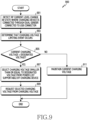
- FIG. 9 is a flowchart 900 illustrating an operation of controlling a charging voltage by using an Rp value change in an electronic device according to an embodiment of the disclosure, not falling under the scope of the claims.
- the electronic device may be the electronic device 101 of FIG. 1 .
- the operations of FIG. 9 described below may be at least some of the detailed operations of operations 401, 403, and 405 of FIG. 4 .
- an electronic device e.g., the processor 120 of FIG. 1 and/or the PDIC driver 225 of FIG. 2
- an electronic device may detect that an Rp current level is changed in a state where a USB device (e.g., the USB device 255 of FIG. 2 ) is connected through a USB connector (e.g., the connection terminal 178 of FIG. 1 and/or the USB connector 209 of FIG. 2 ).
- the PDIC driver 225 may determine that, in addition to the state where the PD charging device 251 has been connected to the electronic device 101, the USB device 255 also has been connected thereto.
- the electronic device e.g., the processor 120 and/or the PDIC driver 225
- the electronic device may determine that a charging voltage limiting event occurs.
- the PDIC driver 225 may be aware that the charging voltage limitation is required in order to prevent the additionally connected USB device 255 from being damaged due to the charging voltage provided from the charging device 251.
- the electronic device may determine whether the current charging voltage is greater than a designated voltage.
- the PDIC driver 225 may compare the current charging voltage with a designated voltage to determine whether the current charging voltage is greater than the designated voltage.
- the current charging voltage may be identified through the charging driver 223.
- the electronic device e.g., the processor 120 and/or the charging driver 223 may select a charging voltage smaller than or equal to a designated voltage from a list of powers supportable by the charging device, in operation 907.
- the list of powers supportable by the charging device 251 may indicate that the charging device 251 may support 5V and 9V.
- the charging driver 223 may select 5V, which is the same as the designated voltage (e.g., about 5V), from among 5V and 9V.
- the charging driver 223 may transmit a signal including information about the selected charging voltage to the PDIC driver 225.
- the electronic device e.g., the processor 120 and/or the PDIC driver 225
- the electronic device may request the charging device to provide the selected charging voltage 251.
- Operation 909 may be the same as operation 509 of FIG. 5 .
- the electronic device e.g., the processor 120 and/or the PDIC driver 225
- the PDIC driver 225 may maintain the current charging voltage instead of adjusting the same to a different charging voltage because the USB device 255 is not damaged even if the current charging voltage provided from the charging device 251 is provided to the USB device 255.
- FIGS. 1 to 9 a method for controlling a charging voltage of the charging device 251 in the electronic device 101 has been described, in order to prevent the USB device 255 from being damaged due to the charging voltage output from the charging device 251 in a state where the USB device (for example, the USB device 255 of FIG. 2 ) and the charging device (for example, the charging device 251 of FIG. 2 ) are connected to the electronic device 101.
- damage of the USB device may be prevented using other methods. For example, by applying an over voltage protection (OVP) circuit to the V BUS pin of the USB device 255, it is possible to prevent the USB device 255 from being damaged due a high voltage output from the charging device 251.
- OVP over voltage protection
- the USB Type-C dual gender 253 may be designed to include at least one of a buck converter, a boost converter, or a buck-boost converter.
- FIG. 10 is a block diagram illustrating the structure of a USB Type-C dual gender 1000 according to an embodiment of the disclosure, not falling under the scope of the claims.
- the USB Type-C dual gender 1000 may include Type-C connector 1 1001, Type-C connector 2 1003, Type-C connector 3 1005, a PDIC 1011, and a boost converter 1013, a buck converter 1015, and a first switch 1021, a second switch 1023, and a third switch 1025.
- Type-C connector 1 1001 may be a plug that can be inserted into the USB connector of the electronic device 101 (e.g., the USB connector 209 of FIG. 2 ).
- Type-C connector 1 1001 may be designed to be connected to a USB connector having a pin structure, as shown in FIG. 3 .
- Type-C connector 1 1001 may have a symmetrical structure so as to be connected to the USB connector 209 of the electronic device 101 regardless of directionality.
- each of Type-C connector 2 1003 and Type-C connector 3 1005 may be a receptacle socket configured to be connectable with a charging device and/or a USB device.
- Each of Type-C connector 2 1003 and Type-C connector 3 1005 may be configured to have a pin structure as shown in FIG. 3 .
- Type-C connector 2 1003 may be a socket connected to the PD charging device.
- Type-C connector 3 1005 may be a socket connected to the USB device.
- the PDIC 1011 may detect the connection of the electronic device 101 and the charging device to each of Type-C connector 1 1001 and Type-C connector 2 1003, based on the resistance value detected through a CC pin of Type-C connector 1 1001 and a CC pin of Type-C connector 2 1003. For example, if the Rp resistance (e.g., 56 ⁇ ) is recognized by the CC pin of Type-C connector 1 1001 and the CC pin of Type-C connector 2 1003, the PDIC 1011 may determine that the electronic device 101 is connected to Type-C connector 1 1001 and the charging device is connected to Type-C connector 2 1003.
- the Rp resistance e.g., 56 ⁇
- the PDIC 1011 may output a control signal to at least one of the boost converter 1013, the buck converter 1015, and the first switch 1021, the second switch 1023, or the third switch 1025, so as to perform control such that the high voltage of the charging device, input through Type-C connector 2 1003, is provided to Type-C connector 1 1001 and a voltage smaller than or equal to the designated voltage is provided to Type-C connector 3 1005.
- the designated voltage may be configured based on the maximum voltage supportable by the USB device connected to Type-C connector 3 1005.
- the boost converter 1013 may boost up the input voltage, and the buck converter 1015 may cut down the input voltage.
- the boost converter 1013 and the buck converter 1015 may boost up and/or cut down the input voltage based on the control signal of the PDIC 1011 to output the boosted-up or cut-down voltage.
- the boost converter 1013 may boost up the input voltage according to the control signal of the PDIC 1011, and the buck converter 1015 may cut down the input voltage according to the control signal of the PDIC 1011 so as to output a voltage smaller than or equal to the designated voltage.
- the boost converter 1013 and the buck converter 1015 may be replaced by at least one buck boost converter according to an embodiment.
- FIG. 11 is a flowchart 1100 illustrating an operation of controlling a charging voltage from a charging device by a USB Type-C dual gender 1000 according to an embodiment of the disclosure, not falling under the scope of the claims.
- a USB Type-C dual gender (e.g., the PDIC 1011 of FIG. 10 ) according to various embodiments may detect the connection of the charging device through a first socket (for example, Type-C connector 2 1003 of FIG. 10 ) in a state where the electronic device 101 is connected to the USB Type-C dual gender 1000.
- a first socket for example, Type-C connector 2 1003 of FIG. 10
- Rp resistance e.g., 56 ⁇
- the PDIC 1011 may determine that, in addition to the state where the electronic device 101 has been connected to the USB Type-C dual gender 1000, the charging device has been connected through Type-C connector 2 1003.
- the USB Type-C dual gender may control a buck-boost circuit and at least one switch so as to control an output voltage to be provided to the second socket (e.g., Type-C connector 3 1005 of FIG. 10 ).
- the PDIC 1011 may output a control signal to at least one of a buck-boost circuit (e.g., the boost converter 1013 and the buck converter 1015 of FIG.
- the first switch 1021, the second switch 1023, and/or the third switch 1025 so as to perform control such that the high voltage of the charging device, input through the first socket (e.g., Type-C connector 2 1003), is cut down to a voltage smaller than or equal to the designated voltage and to be provided to the second socket (e.g., Type-C connector 3 1005).
- the first socket e.g., Type-C connector 2 1003
- the second socket e.g., Type-C connector 3 1005
- the DC-DC converter is added to the USB Type-C dual gender 1000 and cuts down the high voltage output from the charging device 251 to a voltage supportable by the USB device, so that it is possible to prevent the USB device from generating heat and becoming damaged without control by the electronic device 101.
- an operating method of the electronic device 101 includes: detecting a connection of the charging device (for example, the PD charging device 251 of FIG. 2 ) and the USB device (for example, the USB device 255 of FIG. 2 ) to the electronic device 101 through a USB connector (for example, the USB connector 209 of FIG. 2 ) provided in the electronic device 101; in response to the connection of the charging device 251-and the USB device 255 to the electronic device 101, determining a charging voltage satisfying a designated condition; and requesting the charging device to provide the determined charging voltage through the USB connector 209.
- the designated condition is configured based on a maximum voltage, which is supportable by the USB device.
- the operation of determining the charging voltage satisfying the designated condition may include: if the charging device 251 and the USB device 255 are connected to the electronic device 101, acquiring, from the charging device 251, a list including information about charging voltages supportable by the charging device 251; and determining, as a charging voltage of the electronic device 101, a charging voltage smaller than or equal to the designated voltage among charging voltages supportable by the charging device 251.
- the operation of determining the charging voltage satisfying the designated condition may include: if the charging device 251 and the USB device 255 are connected to the electronic device 101, acquiring, from the charging device 251, a list including information about charging voltages supportable by the charging device 251; selecting one charging voltage from among the charging voltages supportable by the charging device 251; and comparing the selected charging voltage with a designated voltage, and determining whether to request the charging device 251 to provide the selected charging voltage.
- the operation of determining whether to request the charging device 251 to provide the selected charging voltage may include: if the selected charging voltage is smaller than or equal to the designated voltage, determining requesting the charging device 251 to provide the selected charging voltage; if the selected charging voltage is greater than the designated voltage, reselecting another charging voltage from among the charging voltages included in the acquired list; and comparing the another reselected charging voltage with a designated voltage, and determining whether to request the charging device to provide the reselected charging voltage 251.
- the operation of determining the charging voltage satisfying the designated condition may include: if the charging device 251 and the USB device 255 are connected to the electronic device 101, comparing a current charging voltage received from the charging device 251 with a designated voltage; and if the current charging voltage is greater than the designated voltage, reselecting a charging voltage smaller than or equal to the designated voltage from among charging voltages supportable by the charging device 251.
- the operation of detecting the connection of the charging device 251 and the USB device 255 to the electronic device 101 through the USB connector 209 provided in the electronic device 101 may include: detecting the connection of the charging device 251 and the USB device 255 to the electronic device 101 through the USB connector 209, based on at least one of a role change of the electronic device 101 for power, identification information of the USB device 255, or a change in a current level recognized through a CC pin of the USB connector 209.
- the operation of detecting the connection of the charging device 251 and the USB device 255 to the electronic device 101 may include: detecting that a detach event occurs based on a resistance value recognized by the CC pin of the USB connector 209 in a state where the role of the electronic device 101 corresponds to a source device for providing a voltage; determining whether the role of the electronic device is switched to a sink device for receiving a voltage within a designated time from a time point at which the detach event occurs, based on the resistance value recognized by the CC pin of the USB connector 209; and if the role of the electronic device 101 is switched to the sink device for receiving the voltage within the designated time from the time point at which the detach event occurs, determining that, in addition to the state where the USB device 255 has been connected to the electronic device 101 through the USB connector 209, the charging device 251 also has been connected thereto.
- the operation of detecting the connection of the charging device 251 and the USB device 255 to the electronic device 101 may include: detecting the connection of the USB device 255 to the USB connector 209 based on a resistance value recognized by a CC pin of the USB connector 209; acquiring identification information of the USB device 255 from the USB device 255 and storing the same; and detecting the occurrence of the detach event in a state where the identification information of the USB device 255 has been stored.
- the operation of detecting the connection of the charging device 251 and the USB device 255 to the electronic device 101 may include: detecting a current level change by the CC pin of the USB connector 209; and if the current level change satisfies a designated condition, determining that, in addition to the state where the charging device 251 has been connected to the electronic device 101 through the USB connector 209, the USB device 255 also has been connected thereto.
- respective operations may be performed in sequence, but are not necessarily performed sequentially.
- the sequence of respective operations may be changed, and at least two operations may be performed in parallel.
- the electronic device may be one of various types of electronic devices.
- the electronic devices may include, for example, a portable communication device (e.g., a smartphone), a computer device, a portable multimedia device, a portable medical device, a camera, a wearable device, or a home appliance. According to an embodiment of the disclosure, the electronic devices are not limited to those described above.
- module may include a unit implemented in hardware, software, or firmware, and may interchangeably be used with other terms, for example, “logic,” “logic block,” “part,” or “circuitry”.
- a module may be a single integral component, or a minimum unit or part thereof, adapted to perform one or more functions.
- the module may be implemented in a form of an application-specific integrated circuit (ASIC).
- ASIC application-specific integrated circuit
- Various embodiments as set forth herein may be implemented as software (e.g., the program 140) including one or more instructions that are stored in a storage medium (e.g., internal memory 136 or external memory 138) that is readable by a machine (e.g., the electronic device 101).
- a processor e.g., the processor 120
- the machine e.g., the electronic device 101
- the one or more instructions may include a code generated by a complier or a code executable by an interpreter.
- the machine-readable storage medium may be provided in the form of a non-transitory storage medium.
- non-transitory simply means that the storage medium is a tangible device, and does not include a signal (e.g., an electromagnetic wave), but this term does not differentiate between where data is semi-permanently stored in the storage medium and where the data is temporarily stored in the storage medium.
- a method may be included and provided in a computer program product.
- the computer program product may be traded as a product between a seller and a buyer.
- the computer program product may be distributed in the form of a machine-readable storage medium (e.g., compact disc read only memory (CD-ROM)), or be distributed (e.g., downloaded or uploaded) online via an application store (e.g., PlayStore TM ), or between two user devices (e.g., smart phones) directly. If distributed online, at least part of the computer program product may be temporarily generated or at least temporarily stored in the machine-readable storage medium, such as memory of the manufacturer's server, a server of the application store, or a relay server.
- CD-ROM compact disc read only memory
- an application store e.g., PlayStore TM
- two user devices e.g., smart phones
- each component e.g., a module or a program of the above-described components may include a single entity or multiple entities.
- a plurality of components e.g., modules or programs
- the integrated component may still perform one or more functions of each of the plurality of components in the same or similar manner as they are performed by a corresponding one of the plurality of components before the integration.
- operations performed by the module, the program, or another component may be carried out sequentially, in parallel, repeatedly, or heuristically, or one or more of the operations may be executed in a different order or omitted, or one or more other operations may be added.
Landscapes
- Engineering & Computer Science (AREA)
- Theoretical Computer Science (AREA)
- General Engineering & Computer Science (AREA)
- Physics & Mathematics (AREA)
- General Physics & Mathematics (AREA)
- Microelectronics & Electronic Packaging (AREA)
- Computer Hardware Design (AREA)
- Power Engineering (AREA)
- Charge And Discharge Circuits For Batteries Or The Like (AREA)
Claims (13)
- Elektronische Vorrichtung (101), die Folgendes umfasst:einen Universal Serial Bus(USB)-Anschluss (209), der mit einer Ladevorrichtung (251) und/oder einer USB-Vorrichtung (255) durch eine duale Steckverbindung (253) verbunden werden kann; undmindestens einen Prozessor (120), der mit dem USB-Anschluss (209) elektrisch gekoppelt ist,wobei der mindestens eine Prozessor (120) konfiguriert ist zum:Erkennen (401) einer Verbindung der Ladevorrichtung (251) und der USB-Vorrichtung (255) mit der elektronischen Vorrichtung (101) durch die duale Steckverbindung, die mit dem USB-Anschluss (209) verbunden ist,Bestimmen (501), ob ein Abtrennereignis in einem Zustand auftritt, in dem die USB-Vorrichtung (255) mit der elektronischen Vorrichtung (101) durch die duale Steckverbindung verbunden ist, die mit dem USB-Anschluss (209) verbunden ist,als Antwort auf die Erkennung (501) des Abtrennereignisses, Bestimmen (503), ob ein Empfängeranschluss innerhalb einer bestimmten Zeit ab einem Zeitpunkt auftritt, zu dem das Abtrennereignis auftritt, wobei die Erkennung des Empfängeranschlusses innerhalb der bestimmten Zeit das Erkennen anzeigt, dass die Ladevorrichtung (251) verbunden ist, während die USB-Vorrichtung (255) verbunden ist,als Antwort auf die Erkennung (503) des Empfängeranschlusses innerhalb der bestimmten Zeit, Bestimmen (403) einer Ladespannung, die eine bestimmte Bedingung erfüllt, wobei die bestimmte Bedingung basierend auf einer Maximalspannung konfiguriert ist, die von der USB-Vorrichtung (255) unterstützt werden kann, undAuffordern (405) der Ladevorrichtung (251), die bestimmte Ladespannung über den USB-Anschluss (209) bereitzustellen.
- Elektronische Vorrichtung (101) nach Anspruch 1, wobei, wenn die Ladevorrichtung (251) und die USB-Vorrichtung (253) mit der elektronischen Vorrichtung (101) verbunden sind, der mindestens eine Prozessor (120) ferner konfiguriert ist zum:Erfassen einer Liste, die Informationen über Ladespannungen enthält, die von der Ladevorrichtung (251) unterstützt werden können, von der Ladevorrichtung (251), undBestimmen einer Ladespannung, die kleiner als oder gleich einer bestimmten Spannung ist, als die Ladespannung der elektronischen Vorrichtung (101) unter Ladespannungen, die von der Ladevorrichtung (251) unterstützt werden können.
- Elektronische Vorrichtung (101) nach Anspruch 1, wobei, wenn die Ladevorrichtung (251) und die USB-Vorrichtung (255) mit der elektronischen Vorrichtung (101) verbunden sind, der mindestens eine Prozessor (120) ferner konfiguriert ist zum:Erfassen einer Liste, die Informationen über Ladespannungen enthält, die von der Ladevorrichtung (251) unterstützt werden können, von der Ladevorrichtung (251),Auswählen einer Ladespannung aus den Ladespannungen, die von der Ladevorrichtung (251) unterstützt werden können, undVergleichen der ausgewählten Ladespannung mit einer bestimmten Spannung und Bestimmen, ob die Ladevorrichtung (251) aufgefordert werden soll, die ausgewählte Ladespannung bereitzustellen.
- Elektronische Vorrichtung (101) nach Anspruch 3, wobei der mindestens eine Prozessor (120) ferner konfiguriert ist zum:wenn die ausgewählte Ladespannung kleiner als oder gleich der bestimmten Spannung ist, Auffordern der Ladevorrichtung (251), die ausgewählte Ladespannung bereitzustellen,wenn die ausgewählte Ladespannung größer als die bestimmte Spannung ist, erneuten Auswählen einer anderen Ladespannung aus den Ladespannungen, die in der erfassten Liste enthalten sind, undVergleichen der anderen neu ausgewählten Ladespannung mit der bestimmten Spannung und Bestimmen, ob die Ladevorrichtung (251) aufgefordert werden soll, die andere neu ausgewählte Ladespannung bereitzustellen.
- Elektronische Vorrichtung nach Anspruch 1, wobei der mindestens eine Prozessor (120) ferner konfiguriert ist zum:wenn die Ladevorrichtung (251) und die USB-Vorrichtung (255) mit der elektronischen Vorrichtung (101) verbunden sind, Vergleichen einer aktuellen Ladespannung, die von der Ladevorrichtung (251) empfangen wird, mit einer bestimmten Spannung,wenn die aktuelle Ladespannung größer als die bestimmte Spannung ist, Auswählen einer Ladespannung, die kleiner als oder gleich der bestimmten Spannung ist, aus Ladespannungen, die von der Ladevorrichtung unterstützt werden können, undAuffordern der Ladevorrichtung (251), die ausgewählte Ladespannung über den USB-Anschluss (209) bereitzustellen.
- Elektronische Vorrichtung (101) nach Anspruch 1, wobei der mindestens eine Prozessor (120) ferner konfiguriert ist, um die Verbindung der Ladevorrichtung (251) und der USB-Vorrichtung (255) mit der elektronischen Vorrichtung (101) über den USB-Anschluss (209) zu erkennen, basierend auf einer Rollenänderung, die sich auf die Leistung der elektronischen Vorrichtung bezieht, Identifikationsinformationen der USB-Vorrichtung (255) und/oder einer Änderung eines Strompegels, der durch einen CC-Pin des USB-Anschlusses (209) erkannt wird.
- Elektronische Vorrichtung (101) nach Anspruch 6, wobei der mindestens eine Prozessor (120) ferner konfiguriert ist zum:Erkennen des Auftretens des Abtrennereignisses basierend auf einem Widerstandswert, der von einem CC-Pin des USB-Anschlusses in einem Zustand erkannt wird, in dem eine Rolle der elektronischen Vorrichtung einer Quellenvorrichtung zum Bereitstellen einer Spannung entspricht,basierend auf dem Widerstandswert, der von dem CC-Pin des USB-Anschlusses (209) erkannt wird, Bestimmen, ob die Rolle der elektronischen Vorrichtung (101) auf eine Empfängervorrichtung umgeschaltet wird, um eine Spannung innerhalb einer bestimmten Zeit ab einem Zeitpunkt zu empfangen, zu dem das Abtrennereignis auftritt, undwenn die Rolle der elektronischen Vorrichtung (101) auf die Empfängervorrichtung umgeschaltet wird, um eine Spannung innerhalb der bestimmten Zeit ab dem Zeitpunkt zu empfangen, zu dem das Abtrennereignis auftritt, Bestimmen, dass zusätzlich zu dem Zustand, in dem die USB-Vorrichtung (255) mit der elektronischen Vorrichtung (101) über den USB-Anschluss (209) verbunden war, die Ladevorrichtung (251) mit der elektronischen Vorrichtung (101) verbunden ist.
- Elektronische Vorrichtung (101) nach Anspruch 7, wobei der mindestens eine Prozessor (120) ferner konfiguriert ist zum:Erkennen einer Verbindung der USB-Vorrichtung (255) mit dem USB-Anschluss (209) basierend auf dem Widerstandswert, der von dem CC-Pin des USB-Anschlusses (209) erkannt wird,Erfassen von Identifikationsinformationen der USB-Vorrichtung (255) von der USB-Vorrichtung und Speichern der erfassten Identifikationsinformationen,wenn das Abtrennereignis in einem Zustand auftritt, in dem die Identifikationsinformationen der USB-Vorrichtung (255) gespeichert wurden, und wenn die Rolle der elektronischen Vorrichtung (101) auf die Empfängervorrichtung umgeschaltet wird, um eine Spannung innerhalb der bestimmten Zeit ab dem Zeitpunkt zu empfangen, zu dem das Abtrennereignis auftritt, Bestimmen, dass zusätzlich zu dem Zustand, in dem die USB-Vorrichtung (255) mit der elektronischen Vorrichtung über den USB-Anschluss (209) verbunden war, die Ladevorrichtung (251) mit der elektronischen Vorrichtung (101) verbunden ist.
- Elektronische Vorrichtung (101) nach Anspruch 1, wobei der Prozessor (120) konfiguriert ist zum:Erkennen einer Strompegeländerung durch einen CC-Pin des USB-Anschlusses (209), undwenn die Strompegeländerung eine bestimmte Bedingung erfüllt, Bestimmen, dass zusätzlich zu einem Zustand, in dem die Ladevorrichtung (251) mit der elektronischen Vorrichtung (101) über den USB-Anschluss (209) verbunden war, die USB-Vorrichtung (255) mit der elektronischen Vorrichtung (101) verbunden ist.
- Betriebsverfahren einer elektronischen Vorrichtung (101), wobei das Betriebsverfahren Folgendes umfasst:Erkennen (401) einer Verbindung einer Ladevorrichtung (251) und einer Universal Serial Bus(USB)-Vorrichtung (255) mit der elektronischen Vorrichtung (101) durch eine duale Steckverbindung, die mit einem USB-Anschluss (209) verbunden ist, der in der elektronischen Vorrichtung (101) bereitgestellt ist;Bestimmen (501), ob ein Abtrennereignis in einem Zustand auftritt, in dem die USB-Vorrichtung (255) mit der elektronischen Vorrichtung (101) durch die duale Steckverbindung verbunden ist, die mit dem USB-Anschluss (209) verbunden ist;als Antwort auf die Erkennung (501) des Abtrennereignisses, Bestimmen (503), ob ein Empfängeranschluss innerhalb einer bestimmten Zeit ab einem Zeitpunkt auftritt, zu dem das Abtrennereignis auftritt, wobei die Erkennung des Empfängeranschlusses innerhalb der bestimmten Zeit das Erkennen anzeigt, dass die Ladevorrichtung (251) verbunden ist, während die USB-Vorrichtung (255) verbunden ist;als Antwort auf die Erkennung (503) des Empfängeranschlusses innerhalb der bestimmten Zeit, Bestimmen (403) einer Ladespannung, die eine bestimmte Bedingung erfüllt, wobei die bestimmte Bedingung basierend auf einer Maximalspannung konfiguriert ist, die von der USB-Vorrichtung (255) unterstützt werden kann; undAuffordern (405) der Ladevorrichtung (251), die bestimmte Ladespannung über den USB-Anschluss (209) bereitzustellen.
- Betriebsverfahren nach Anspruch 10, wobei das Bestimmen der Ladespannung, die die bestimmte Bedingung erfüllt, Folgendes umfasst:wenn die Ladevorrichtung (251) und die USB-Vorrichtung (255) mit der elektronischen Vorrichtung (101) verbunden sind, Erfassen (251) einer Liste, die Informationen über Ladespannungen enthält, die von der Ladevorrichtung (251) unterstützt werden können, von der Ladevorrichtung; undBestimmen einer Ladespannung, die kleiner als oder gleich einer bestimmten Spannung ist, als die Ladespannung der elektronischen Vorrichtung (101) unter Ladespannungen, die von der Ladevorrichtung (251) unterstützt werden können.
- Betriebsverfahren nach Anspruch 10, wobei das Bestimmen der Ladespannung, die die bestimmte Bedingung erfüllt, Folgendes umfasst:wenn die Ladevorrichtung (251) und die USB-Vorrichtung (255) mit der elektronischen Vorrichtung (101) verbunden sind, Erfassen einer Liste, die Informationen über Ladespannungen enthält, die von der Ladevorrichtung (251) unterstützt werden können, von der Ladevorrichtung (251);Auswählen einer Ladespannung aus den Ladespannungen, die von der Ladevorrichtung (251) unterstützt werden können; undVergleichen der ausgewählten Ladespannung mit einer bestimmten Spannung und Bestimmen, ob die Ladevorrichtung (251) aufgefordert werden soll, die ausgewählte Ladespannung bereitzustellen.
- Betriebsverfahren nach Anspruch 12, wobei das Bestimmen, ob die Ladevorrichtung (251) aufgefordert werden soll, die ausgewählte Ladespannung bereitzustellen, Folgendes umfasst:wenn die ausgewählte Ladespannung kleiner als oder gleich der bestimmten Spannung ist, Auffordern der Ladevorrichtung (251), die ausgewählte Ladespannung bereitzustellen;wenn die ausgewählte Ladespannung größer als die bestimmte Spannung ist, erneutes Auswählen einer anderen Ladespannung aus den Ladespannungen, die in der erfassten Liste enthalten sind; undVergleichen der anderen neu ausgewählten Ladespannung mit der bestimmten Spannung und Bestimmen, ob die Ladevorrichtung (251) aufgefordert werden soll, die andere neu ausgewählte Ladespannung bereitzustellen.
Applications Claiming Priority (1)
| Application Number | Priority Date | Filing Date | Title |
|---|---|---|---|
| KR1020190092308A KR102651715B1 (ko) | 2019-07-30 | 2019-07-30 | Usb 장치의 손상을 방지하기 위한 전자 장치 및 그의 동작 방법 |
Publications (2)
| Publication Number | Publication Date |
|---|---|
| EP3771987A1 EP3771987A1 (de) | 2021-02-03 |
| EP3771987B1 true EP3771987B1 (de) | 2023-06-14 |
Family
ID=71846265
Family Applications (1)
| Application Number | Title | Priority Date | Filing Date |
|---|---|---|---|
| EP20188347.7A Active EP3771987B1 (de) | 2019-07-30 | 2020-07-29 | Elektronische vorrichtung zur verhinderung der beschädigung von usb-vorrichtungen und betriebsverfahren dafür |
Country Status (5)
| Country | Link |
|---|---|
| US (1) | US11379026B2 (de) |
| EP (1) | EP3771987B1 (de) |
| KR (1) | KR102651715B1 (de) |
| CN (1) | CN112310756B (de) |
| WO (1) | WO2021020900A1 (de) |
Families Citing this family (6)
| Publication number | Priority date | Publication date | Assignee | Title |
|---|---|---|---|---|
| KR102787543B1 (ko) * | 2019-09-20 | 2025-04-01 | 삼성전자주식회사 | 외부 장치와의 연결을 지원하는 전자 장치 및 그 외부 장치와 연결하여 사용할 때 소모 전류를 감소시키는 방법 |
| CN110879792B (zh) * | 2019-11-13 | 2024-01-23 | Oppo广东移动通信有限公司 | 电子设备及其接口控制方法 |
| KR20220161817A (ko) * | 2021-05-31 | 2022-12-07 | 삼성전자주식회사 | 외부 장치와의 연결을 지원하는 전자 장치 및 그의 동작 방법 |
| US12259836B2 (en) * | 2021-09-24 | 2025-03-25 | Intel Corporation | Peer-influenced enhanced USB power delivery |
| CN114123379B (zh) * | 2021-10-18 | 2023-12-15 | 东风柳州汽车有限公司 | 电池包充电连接确认方法及装置 |
| TWI867815B (zh) * | 2023-10-30 | 2024-12-21 | 威鋒電子股份有限公司 | Usb纜線、電子標示裝置及usb連接器的溼度偵測方法 |
Citations (3)
| Publication number | Priority date | Publication date | Assignee | Title |
|---|---|---|---|---|
| US20170256968A1 (en) * | 2016-03-04 | 2017-09-07 | Samsung Electronics Co., Ltd. | Electronic device and external device charging method |
| FR3092707A1 (fr) * | 2019-02-12 | 2020-08-14 | Stmicroelectronics (Grenoble 2) Sas | Equipement de test de dispositif USB-PD |
| DE112020005079T5 (de) * | 2020-03-31 | 2022-08-11 | WESTERN DIGITAL TECHNOLOGIES, Inc. | Dual-verbinder-speicherungssystem und verfahren zum gleichzeitigen bereitstellen von leistungs- und speicherzugriff auf eine rechnervorrichtung |
Family Cites Families (41)
| Publication number | Priority date | Publication date | Assignee | Title |
|---|---|---|---|---|
| US7679317B2 (en) * | 2005-02-15 | 2010-03-16 | Research In Motion Limited | Systems and methods for charging a chargeable USB device |
| US8070067B2 (en) * | 2005-12-22 | 2011-12-06 | Industrial Technology Research Institute | Receptacles for removable electrical interface devices |
| US7644217B2 (en) * | 2007-03-02 | 2010-01-05 | Microchip Technology Incorporated | Detecting connection to a USB host or hub without using an extra status input |
| KR100791583B1 (ko) | 2007-03-31 | 2008-01-04 | (주)융스그룹 | 유에스비 커넥터 겸용 이어폰 젠더 |
| KR101006160B1 (ko) | 2008-09-09 | 2011-01-07 | 김기형 | 유에스비 커넥터를 위한 멀티 젠더 |
| US20100070659A1 (en) | 2008-09-17 | 2010-03-18 | Kenneth Ma | Method and system for operating and/or charging a battery powered usb device based on a usb port type |
| KR20120009890A (ko) | 2010-07-22 | 2012-02-02 | (주)금오전자 | 휴대단말기용 젠더 |
| US20120198101A1 (en) * | 2011-01-27 | 2012-08-02 | Brewster Porcella | Mobile device peripheral detection with independent state machines |
| US9395780B2 (en) | 2011-04-21 | 2016-07-19 | Texas Instruments Incorporated | USB bridge circuit gating RID—A and RID—GND for IDGND |
| US10152104B2 (en) * | 2012-06-15 | 2018-12-11 | Texas Instruments Incorporated | Policy engine startup procedure for a default provider in USB power delivery |
| US20140208134A1 (en) * | 2013-01-21 | 2014-07-24 | Texas Instruments Incorporated | Host controller interface for universal serial bus (usb) power delivery |
| US9496726B2 (en) * | 2013-07-31 | 2016-11-15 | Leviton Manufacturing Co., Inc. | Multiport USB charger |
| US9645962B2 (en) * | 2013-09-26 | 2017-05-09 | Delphi Technologies, Inc. | Flexible mobile device connectivity to automotive systems with USB hubs |
| US10063073B2 (en) * | 2014-05-21 | 2018-08-28 | Dialog Semiconductor Inc. | USB power converter with bleeder circuit for fast correction of output voltage by discharging output capacitor |
| US9590441B2 (en) * | 2014-07-22 | 2017-03-07 | Cypress Semiconductor Corporation | Multi-standard compliant USB battery charging scheme with detection of host disconnection in ACA-DOCK mode |
| CN104393627B (zh) * | 2014-08-29 | 2017-06-30 | 展讯通信(上海)有限公司 | Usb充电器、移动终端和充电控制方法 |
| US9400546B1 (en) * | 2015-06-19 | 2016-07-26 | Cypress Semiconductor Corporation | Low-power implementation of Type-C connector subsystem |
| US10088884B2 (en) * | 2015-10-23 | 2018-10-02 | Nxp B.V. | Communications for power delivery solutions |
| CN113031740B (zh) * | 2015-11-13 | 2024-07-12 | 德州仪器公司 | 具有供电合约协商能力的端口控制器 |
| CN105305565B (zh) * | 2015-11-26 | 2018-02-23 | 英特格灵芯片(天津)有限公司 | 一种充电保护及识别电路及待充电设备 |
| US10186881B2 (en) * | 2016-03-21 | 2019-01-22 | Microsoft Technology Licensing, Llc | Regulating charging port attach and detach |
| GB2549958A (en) * | 2016-05-03 | 2017-11-08 | Displaylink Uk Ltd | USB power delivery |
| US10761553B2 (en) * | 2016-06-17 | 2020-09-01 | Qualcomm Incorporated | Universal serial bus (USB) cable type detection and control techniques |
| US10372568B2 (en) * | 2016-07-20 | 2019-08-06 | Canon Kabushiki Kaisha | Electronic device being connectable to external device, and method of controlling electronic device being connectable to extenal device |
| KR102660519B1 (ko) * | 2016-08-01 | 2024-04-25 | 삼성전자주식회사 | 외부 장치를 인식하는 방법 및 이를 지원하는 전자 장치 |
| US10331596B2 (en) | 2016-09-07 | 2019-06-25 | Futurewei Technologies, Inc. | USB type-C connector with a secondary port |
| KR102576430B1 (ko) | 2016-11-18 | 2023-09-08 | 삼성전자주식회사 | 인터페이스 장치 |
| US10331579B2 (en) * | 2016-11-22 | 2019-06-25 | Qualcomm Incorporated | Universal serial bus (USB) system supporting display alternate mode functionality on a USB type-C adapter |
| US10241954B2 (en) * | 2016-12-31 | 2019-03-26 | Intel Corporation | Universal serial bus type-C power delivery |
| KR102677472B1 (ko) * | 2017-02-10 | 2024-06-24 | 삼성전자주식회사 | 외부 장치로 전력을 공급하는 장치 및 이를 위한 방법 |
| US10461555B2 (en) * | 2017-05-18 | 2019-10-29 | Dialog Semiconductor (Uk) Limited | Battery charging for mobile devices |
| KR102439078B1 (ko) * | 2017-06-23 | 2022-09-01 | 삼성전자주식회사 | 전자 장치 및 그의 충전 제어 방법 |
| US10712801B2 (en) * | 2017-06-30 | 2020-07-14 | Intel Corporation | USB type-C power delivery management |
| KR102486833B1 (ko) * | 2017-08-23 | 2023-01-11 | 삼성전자주식회사 | 전자 장치들간의 전원 제어 방법 및 전자 장치 |
| US10489324B2 (en) * | 2017-08-25 | 2019-11-26 | Qualcomm Incorporated | Systems and methods for port management |
| KR102467174B1 (ko) * | 2017-11-14 | 2022-11-16 | 삼성전자주식회사 | Usb 타입의 충전 장치 및 상기 충전 장치의 제어 방법 |
| KR102521653B1 (ko) * | 2017-12-13 | 2023-04-14 | 삼성전자주식회사 | 이물질 검출 회로 및 이를 포함하는 전자 장치 |
| US10955888B2 (en) * | 2018-01-29 | 2021-03-23 | Via Labs, Inc. | Universal serial bus device and method for dynamically defining a power source or sink status for downstream facing ports |
| US11169589B2 (en) * | 2018-12-28 | 2021-11-09 | Intel Corporation | Managing system power in USB-C/USB power delivery systems |
| US10635611B1 (en) * | 2019-01-22 | 2020-04-28 | Intel Corporation | Device, system and method for determining an orientation of a connection to an IO interface |
| JP7581009B2 (ja) * | 2020-10-26 | 2024-11-12 | キヤノン株式会社 | 画像形成装置、画像形成装置の制御方法、及びプログラム |
-
2019
- 2019-07-30 KR KR1020190092308A patent/KR102651715B1/ko active Active
-
2020
- 2020-07-29 EP EP20188347.7A patent/EP3771987B1/de active Active
- 2020-07-29 US US16/941,973 patent/US11379026B2/en active Active
- 2020-07-30 WO PCT/KR2020/010062 patent/WO2021020900A1/en not_active Ceased
- 2020-07-30 CN CN202010753799.7A patent/CN112310756B/zh active Active
Patent Citations (3)
| Publication number | Priority date | Publication date | Assignee | Title |
|---|---|---|---|---|
| US20170256968A1 (en) * | 2016-03-04 | 2017-09-07 | Samsung Electronics Co., Ltd. | Electronic device and external device charging method |
| FR3092707A1 (fr) * | 2019-02-12 | 2020-08-14 | Stmicroelectronics (Grenoble 2) Sas | Equipement de test de dispositif USB-PD |
| DE112020005079T5 (de) * | 2020-03-31 | 2022-08-11 | WESTERN DIGITAL TECHNOLOGIES, Inc. | Dual-verbinder-speicherungssystem und verfahren zum gleichzeitigen bereitstellen von leistungs- und speicherzugriff auf eine rechnervorrichtung |
Also Published As
| Publication number | Publication date |
|---|---|
| EP3771987A1 (de) | 2021-02-03 |
| WO2021020900A1 (en) | 2021-02-04 |
| CN112310756A (zh) | 2021-02-02 |
| US20210034127A1 (en) | 2021-02-04 |
| CN112310756B (zh) | 2024-12-06 |
| KR102651715B1 (ko) | 2024-03-28 |
| US11379026B2 (en) | 2022-07-05 |
| KR20210014356A (ko) | 2021-02-09 |
Similar Documents
| Publication | Publication Date | Title |
|---|---|---|
| US11288407B2 (en) | Method and electronic device for controlling voltage output to external electronic device according to size of voltage detected at signal terminal connected to external electronic device | |
| EP3771987B1 (de) | Elektronische vorrichtung zur verhinderung der beschädigung von usb-vorrichtungen und betriebsverfahren dafür | |
| US11989365B2 (en) | Electronic device including electronic pen and method of controlling communication connection between electronic device and electronic pen | |
| US11368027B2 (en) | Electronic device including control circuits controlling switches connected to charging circuit | |
| US10809826B2 (en) | Electronic device and method for displaying affordance for providing charging of battery of external device through display | |
| US12038798B2 (en) | Method for selectively controlling voltage, and electronic device and external electronic device therefor | |
| US11775040B2 (en) | Electronic device and method for receiving power from external electronic device | |
| KR102915943B1 (ko) | 배터리 충전 장치 및 방법 | |
| US11462998B2 (en) | Apparatus for detecting feedback on voltage supplied from electronic device to external device | |
| US12380054B2 (en) | Electronic device and method for controlling power supply of electronic device | |
| US11489371B2 (en) | Wireless charging device communicating with electronic device and communication method of wireless charging device | |
| EP3629428B1 (de) | Verfahren und vorrichtung zur änderung der impedanz eines in einem verbinder enthaltenen anschlusses | |
| US11556160B2 (en) | Electronic device for adjusting voltage and operating method therefor | |
| KR20210054172A (ko) | 전력 패스 제어 방법 및 이를 지원하는 전자 장치 | |
| US11249559B2 (en) | Electronic device and method for controlling reset of control IC | |
| US20200185979A1 (en) | Device for transferring and receiving wireless power and method for adjusting power thereof | |
| EP4693812A1 (de) | Elektronische vorrichtung zur stromversorgung nach aussen | |
| US12170447B2 (en) | Electronic device for wirelessly charging external electronic device |
Legal Events
| Date | Code | Title | Description |
|---|---|---|---|
| PUAI | Public reference made under article 153(3) epc to a published international application that has entered the european phase |
Free format text: ORIGINAL CODE: 0009012 |
|
| STAA | Information on the status of an ep patent application or granted ep patent |
Free format text: STATUS: THE APPLICATION HAS BEEN PUBLISHED |
|
| AK | Designated contracting states |
Kind code of ref document: A1 Designated state(s): AL AT BE BG CH CY CZ DE DK EE ES FI FR GB GR HR HU IE IS IT LI LT LU LV MC MK MT NL NO PL PT RO RS SE SI SK SM TR |
|
| AX | Request for extension of the european patent |
Extension state: BA ME |
|
| STAA | Information on the status of an ep patent application or granted ep patent |
Free format text: STATUS: REQUEST FOR EXAMINATION WAS MADE |
|
| 17P | Request for examination filed |
Effective date: 20210423 |
|
| RBV | Designated contracting states (corrected) |
Designated state(s): AL AT BE BG CH CY CZ DE DK EE ES FI FR GB GR HR HU IE IS IT LI LT LU LV MC MK MT NL NO PL PT RO RS SE SI SK SM TR |
|
| STAA | Information on the status of an ep patent application or granted ep patent |
Free format text: STATUS: EXAMINATION IS IN PROGRESS |
|
| 17Q | First examination report despatched |
Effective date: 20220131 |
|
| GRAP | Despatch of communication of intention to grant a patent |
Free format text: ORIGINAL CODE: EPIDOSNIGR1 |
|
| STAA | Information on the status of an ep patent application or granted ep patent |
Free format text: STATUS: GRANT OF PATENT IS INTENDED |
|
| INTG | Intention to grant announced |
Effective date: 20230125 |
|
| GRAS | Grant fee paid |
Free format text: ORIGINAL CODE: EPIDOSNIGR3 |
|
| GRAA | (expected) grant |
Free format text: ORIGINAL CODE: 0009210 |
|
| STAA | Information on the status of an ep patent application or granted ep patent |
Free format text: STATUS: THE PATENT HAS BEEN GRANTED |
|
| AK | Designated contracting states |
Kind code of ref document: B1 Designated state(s): AL AT BE BG CH CY CZ DE DK EE ES FI FR GB GR HR HU IE IS IT LI LT LU LV MC MK MT NL NO PL PT RO RS SE SI SK SM TR |
|
| REG | Reference to a national code |
Ref country code: CH Ref legal event code: EP |
|
| REG | Reference to a national code |
Ref country code: DE Ref legal event code: R096 Ref document number: 602020012443 Country of ref document: DE |
|
| REG | Reference to a national code |
Ref country code: AT Ref legal event code: REF Ref document number: 1579733 Country of ref document: AT Kind code of ref document: T Effective date: 20230715 |
|
| REG | Reference to a national code |
Ref country code: LT Ref legal event code: MG9D |
|
| REG | Reference to a national code |
Ref country code: NL Ref legal event code: MP Effective date: 20230614 |
|
| PG25 | Lapsed in a contracting state [announced via postgrant information from national office to epo] |
Ref country code: SE Free format text: LAPSE BECAUSE OF FAILURE TO SUBMIT A TRANSLATION OF THE DESCRIPTION OR TO PAY THE FEE WITHIN THE PRESCRIBED TIME-LIMIT Effective date: 20230614 Ref country code: NO Free format text: LAPSE BECAUSE OF FAILURE TO SUBMIT A TRANSLATION OF THE DESCRIPTION OR TO PAY THE FEE WITHIN THE PRESCRIBED TIME-LIMIT Effective date: 20230914 Ref country code: ES Free format text: LAPSE BECAUSE OF FAILURE TO SUBMIT A TRANSLATION OF THE DESCRIPTION OR TO PAY THE FEE WITHIN THE PRESCRIBED TIME-LIMIT Effective date: 20230614 |
|
| REG | Reference to a national code |
Ref country code: AT Ref legal event code: MK05 Ref document number: 1579733 Country of ref document: AT Kind code of ref document: T Effective date: 20230614 |
|
| PG25 | Lapsed in a contracting state [announced via postgrant information from national office to epo] |
Ref country code: RS Free format text: LAPSE BECAUSE OF FAILURE TO SUBMIT A TRANSLATION OF THE DESCRIPTION OR TO PAY THE FEE WITHIN THE PRESCRIBED TIME-LIMIT Effective date: 20230614 Ref country code: NL Free format text: LAPSE BECAUSE OF FAILURE TO SUBMIT A TRANSLATION OF THE DESCRIPTION OR TO PAY THE FEE WITHIN THE PRESCRIBED TIME-LIMIT Effective date: 20230614 Ref country code: LV Free format text: LAPSE BECAUSE OF FAILURE TO SUBMIT A TRANSLATION OF THE DESCRIPTION OR TO PAY THE FEE WITHIN THE PRESCRIBED TIME-LIMIT Effective date: 20230614 Ref country code: LT Free format text: LAPSE BECAUSE OF FAILURE TO SUBMIT A TRANSLATION OF THE DESCRIPTION OR TO PAY THE FEE WITHIN THE PRESCRIBED TIME-LIMIT Effective date: 20230614 Ref country code: HR Free format text: LAPSE BECAUSE OF FAILURE TO SUBMIT A TRANSLATION OF THE DESCRIPTION OR TO PAY THE FEE WITHIN THE PRESCRIBED TIME-LIMIT Effective date: 20230614 Ref country code: GR Free format text: LAPSE BECAUSE OF FAILURE TO SUBMIT A TRANSLATION OF THE DESCRIPTION OR TO PAY THE FEE WITHIN THE PRESCRIBED TIME-LIMIT Effective date: 20230915 |
|
| PG25 | Lapsed in a contracting state [announced via postgrant information from national office to epo] |
Ref country code: FI Free format text: LAPSE BECAUSE OF FAILURE TO SUBMIT A TRANSLATION OF THE DESCRIPTION OR TO PAY THE FEE WITHIN THE PRESCRIBED TIME-LIMIT Effective date: 20230614 |
|
| PG25 | Lapsed in a contracting state [announced via postgrant information from national office to epo] |
Ref country code: SK Free format text: LAPSE BECAUSE OF FAILURE TO SUBMIT A TRANSLATION OF THE DESCRIPTION OR TO PAY THE FEE WITHIN THE PRESCRIBED TIME-LIMIT Effective date: 20230614 |
|
| PG25 | Lapsed in a contracting state [announced via postgrant information from national office to epo] |
Ref country code: IS Free format text: LAPSE BECAUSE OF FAILURE TO SUBMIT A TRANSLATION OF THE DESCRIPTION OR TO PAY THE FEE WITHIN THE PRESCRIBED TIME-LIMIT Effective date: 20231014 |
|
| PG25 | Lapsed in a contracting state [announced via postgrant information from national office to epo] |
Ref country code: SM Free format text: LAPSE BECAUSE OF FAILURE TO SUBMIT A TRANSLATION OF THE DESCRIPTION OR TO PAY THE FEE WITHIN THE PRESCRIBED TIME-LIMIT Effective date: 20230614 Ref country code: SK Free format text: LAPSE BECAUSE OF FAILURE TO SUBMIT A TRANSLATION OF THE DESCRIPTION OR TO PAY THE FEE WITHIN THE PRESCRIBED TIME-LIMIT Effective date: 20230614 Ref country code: RO Free format text: LAPSE BECAUSE OF FAILURE TO SUBMIT A TRANSLATION OF THE DESCRIPTION OR TO PAY THE FEE WITHIN THE PRESCRIBED TIME-LIMIT Effective date: 20230614 Ref country code: PT Free format text: LAPSE BECAUSE OF FAILURE TO SUBMIT A TRANSLATION OF THE DESCRIPTION OR TO PAY THE FEE WITHIN THE PRESCRIBED TIME-LIMIT Effective date: 20231016 Ref country code: IS Free format text: LAPSE BECAUSE OF FAILURE TO SUBMIT A TRANSLATION OF THE DESCRIPTION OR TO PAY THE FEE WITHIN THE PRESCRIBED TIME-LIMIT Effective date: 20231014 Ref country code: EE Free format text: LAPSE BECAUSE OF FAILURE TO SUBMIT A TRANSLATION OF THE DESCRIPTION OR TO PAY THE FEE WITHIN THE PRESCRIBED TIME-LIMIT Effective date: 20230614 Ref country code: CZ Free format text: LAPSE BECAUSE OF FAILURE TO SUBMIT A TRANSLATION OF THE DESCRIPTION OR TO PAY THE FEE WITHIN THE PRESCRIBED TIME-LIMIT Effective date: 20230614 Ref country code: AT Free format text: LAPSE BECAUSE OF FAILURE TO SUBMIT A TRANSLATION OF THE DESCRIPTION OR TO PAY THE FEE WITHIN THE PRESCRIBED TIME-LIMIT Effective date: 20230614 |
|
| PG25 | Lapsed in a contracting state [announced via postgrant information from national office to epo] |
Ref country code: PL Free format text: LAPSE BECAUSE OF FAILURE TO SUBMIT A TRANSLATION OF THE DESCRIPTION OR TO PAY THE FEE WITHIN THE PRESCRIBED TIME-LIMIT Effective date: 20230614 |
|
| REG | Reference to a national code |
Ref country code: CH Ref legal event code: PL |
|
| PG25 | Lapsed in a contracting state [announced via postgrant information from national office to epo] |
Ref country code: MC Free format text: LAPSE BECAUSE OF FAILURE TO SUBMIT A TRANSLATION OF THE DESCRIPTION OR TO PAY THE FEE WITHIN THE PRESCRIBED TIME-LIMIT Effective date: 20230614 |
|
| REG | Reference to a national code |
Ref country code: DE Ref legal event code: R097 Ref document number: 602020012443 Country of ref document: DE |
|
| REG | Reference to a national code |
Ref country code: BE Ref legal event code: MM Effective date: 20230731 |
|
| PG25 | Lapsed in a contracting state [announced via postgrant information from national office to epo] |
Ref country code: LU Free format text: LAPSE BECAUSE OF NON-PAYMENT OF DUE FEES Effective date: 20230729 |
|
| PG25 | Lapsed in a contracting state [announced via postgrant information from national office to epo] |
Ref country code: MC Free format text: LAPSE BECAUSE OF FAILURE TO SUBMIT A TRANSLATION OF THE DESCRIPTION OR TO PAY THE FEE WITHIN THE PRESCRIBED TIME-LIMIT Effective date: 20230614 Ref country code: LU Free format text: LAPSE BECAUSE OF NON-PAYMENT OF DUE FEES Effective date: 20230729 |
|
| PLBE | No opposition filed within time limit |
Free format text: ORIGINAL CODE: 0009261 |
|
| STAA | Information on the status of an ep patent application or granted ep patent |
Free format text: STATUS: NO OPPOSITION FILED WITHIN TIME LIMIT |
|
| REG | Reference to a national code |
Ref country code: IE Ref legal event code: MM4A |
|
| PG25 | Lapsed in a contracting state [announced via postgrant information from national office to epo] |
Ref country code: DK Free format text: LAPSE BECAUSE OF FAILURE TO SUBMIT A TRANSLATION OF THE DESCRIPTION OR TO PAY THE FEE WITHIN THE PRESCRIBED TIME-LIMIT Effective date: 20230614 Ref country code: CH Free format text: LAPSE BECAUSE OF NON-PAYMENT OF DUE FEES Effective date: 20230731 |
|
| PG25 | Lapsed in a contracting state [announced via postgrant information from national office to epo] |
Ref country code: SI Free format text: LAPSE BECAUSE OF FAILURE TO SUBMIT A TRANSLATION OF THE DESCRIPTION OR TO PAY THE FEE WITHIN THE PRESCRIBED TIME-LIMIT Effective date: 20230614 |
|
| 26N | No opposition filed |
Effective date: 20240315 |
|
| PG25 | Lapsed in a contracting state [announced via postgrant information from national office to epo] |
Ref country code: SI Free format text: LAPSE BECAUSE OF FAILURE TO SUBMIT A TRANSLATION OF THE DESCRIPTION OR TO PAY THE FEE WITHIN THE PRESCRIBED TIME-LIMIT Effective date: 20230614 Ref country code: IT Free format text: LAPSE BECAUSE OF FAILURE TO SUBMIT A TRANSLATION OF THE DESCRIPTION OR TO PAY THE FEE WITHIN THE PRESCRIBED TIME-LIMIT Effective date: 20230614 Ref country code: BE Free format text: LAPSE BECAUSE OF NON-PAYMENT OF DUE FEES Effective date: 20230731 |
|
| PG25 | Lapsed in a contracting state [announced via postgrant information from national office to epo] |
Ref country code: IE Free format text: LAPSE BECAUSE OF NON-PAYMENT OF DUE FEES Effective date: 20230729 |
|
| PG25 | Lapsed in a contracting state [announced via postgrant information from national office to epo] |
Ref country code: IE Free format text: LAPSE BECAUSE OF NON-PAYMENT OF DUE FEES Effective date: 20230729 Ref country code: FR Free format text: LAPSE BECAUSE OF NON-PAYMENT OF DUE FEES Effective date: 20230814 |
|
| PG25 | Lapsed in a contracting state [announced via postgrant information from national office to epo] |
Ref country code: BG Free format text: LAPSE BECAUSE OF FAILURE TO SUBMIT A TRANSLATION OF THE DESCRIPTION OR TO PAY THE FEE WITHIN THE PRESCRIBED TIME-LIMIT Effective date: 20230614 |
|
| PG25 | Lapsed in a contracting state [announced via postgrant information from national office to epo] |
Ref country code: BG Free format text: LAPSE BECAUSE OF FAILURE TO SUBMIT A TRANSLATION OF THE DESCRIPTION OR TO PAY THE FEE WITHIN THE PRESCRIBED TIME-LIMIT Effective date: 20230614 |
|
| GBPC | Gb: european patent ceased through non-payment of renewal fee |
Effective date: 20240729 |
|
| PG25 | Lapsed in a contracting state [announced via postgrant information from national office to epo] |
Ref country code: GB Free format text: LAPSE BECAUSE OF NON-PAYMENT OF DUE FEES Effective date: 20240729 |
|
| PG25 | Lapsed in a contracting state [announced via postgrant information from national office to epo] |
Ref country code: CY Free format text: LAPSE BECAUSE OF FAILURE TO SUBMIT A TRANSLATION OF THE DESCRIPTION OR TO PAY THE FEE WITHIN THE PRESCRIBED TIME-LIMIT; INVALID AB INITIO Effective date: 20200729 |
|
| PG25 | Lapsed in a contracting state [announced via postgrant information from national office to epo] |
Ref country code: HU Free format text: LAPSE BECAUSE OF FAILURE TO SUBMIT A TRANSLATION OF THE DESCRIPTION OR TO PAY THE FEE WITHIN THE PRESCRIBED TIME-LIMIT; INVALID AB INITIO Effective date: 20200729 |
|
| PGFP | Annual fee paid to national office [announced via postgrant information from national office to epo] |
Ref country code: DE Payment date: 20250624 Year of fee payment: 6 |
|
| PG25 | Lapsed in a contracting state [announced via postgrant information from national office to epo] |
Ref country code: TR Free format text: LAPSE BECAUSE OF FAILURE TO SUBMIT A TRANSLATION OF THE DESCRIPTION OR TO PAY THE FEE WITHIN THE PRESCRIBED TIME-LIMIT Effective date: 20230614 |