EP3772061B1 - Stromgeneratorschaltung, vorrichtung mit der stromgeneratorschaltung und elektronisches system - Google Patents
Stromgeneratorschaltung, vorrichtung mit der stromgeneratorschaltung und elektronisches system Download PDFInfo
- Publication number
- EP3772061B1 EP3772061B1 EP20188675.1A EP20188675A EP3772061B1 EP 3772061 B1 EP3772061 B1 EP 3772061B1 EP 20188675 A EP20188675 A EP 20188675A EP 3772061 B1 EP3772061 B1 EP 3772061B1
- Authority
- EP
- European Patent Office
- Prior art keywords
- current
- compensation
- branch
- control
- coupled
- Prior art date
- Legal status (The legal status is an assumption and is not a legal conclusion. Google has not performed a legal analysis and makes no representation as to the accuracy of the status listed.)
- Active
Links
Images


Classifications
-
- G—PHYSICS
- G11—INFORMATION STORAGE
- G11C—STATIC STORES
- G11C13/00—Digital stores characterised by the use of storage elements not covered by groups G11C11/00, G11C23/00, or G11C25/00
- G11C13/0002—Digital stores characterised by the use of storage elements not covered by groups G11C11/00, G11C23/00, or G11C25/00 using resistive RAM [RRAM] elements
- G11C13/0021—Auxiliary circuits
- G11C13/0038—Power supply circuits
-
- G—PHYSICS
- G05—CONTROLLING; REGULATING
- G05F—SYSTEMS FOR REGULATING ELECTRIC OR MAGNETIC VARIABLES
- G05F3/00—Non-retroactive systems for regulating electric variables by using an uncontrolled element, or an uncontrolled combination of elements, such element or such combination having self-regulating properties
- G05F3/02—Regulating voltage or current
- G05F3/08—Regulating voltage or current wherein the variable is DC
- G05F3/10—Regulating voltage or current wherein the variable is DC using uncontrolled devices with non-linear characteristics
- G05F3/16—Regulating voltage or current wherein the variable is DC using uncontrolled devices with non-linear characteristics being semiconductor devices
- G05F3/20—Regulating voltage or current wherein the variable is DC using uncontrolled devices with non-linear characteristics being semiconductor devices using diode- transistor combinations
- G05F3/26—Current mirrors
- G05F3/262—Current mirrors using field-effect transistors only
-
- G—PHYSICS
- G11—INFORMATION STORAGE
- G11C—STATIC STORES
- G11C13/00—Digital stores characterised by the use of storage elements not covered by groups G11C11/00, G11C23/00, or G11C25/00
- G11C13/0002—Digital stores characterised by the use of storage elements not covered by groups G11C11/00, G11C23/00, or G11C25/00 using resistive RAM [RRAM] elements
- G11C13/0004—Digital stores characterised by the use of storage elements not covered by groups G11C11/00, G11C23/00, or G11C25/00 using resistive RAM [RRAM] elements comprising amorphous/crystalline phase transition cells
-
- G—PHYSICS
- G11—INFORMATION STORAGE
- G11C—STATIC STORES
- G11C13/00—Digital stores characterised by the use of storage elements not covered by groups G11C11/00, G11C23/00, or G11C25/00
- G11C13/0002—Digital stores characterised by the use of storage elements not covered by groups G11C11/00, G11C23/00, or G11C25/00 using resistive RAM [RRAM] elements
- G11C13/0021—Auxiliary circuits
- G11C13/0023—Address circuits or decoders
- G11C13/0026—Bit-line or column circuits
-
- G—PHYSICS
- G11—INFORMATION STORAGE
- G11C—STATIC STORES
- G11C13/00—Digital stores characterised by the use of storage elements not covered by groups G11C11/00, G11C23/00, or G11C25/00
- G11C13/0002—Digital stores characterised by the use of storage elements not covered by groups G11C11/00, G11C23/00, or G11C25/00 using resistive RAM [RRAM] elements
- G11C13/0021—Auxiliary circuits
- G11C13/003—Cell access
-
- G—PHYSICS
- G11—INFORMATION STORAGE
- G11C—STATIC STORES
- G11C13/00—Digital stores characterised by the use of storage elements not covered by groups G11C11/00, G11C23/00, or G11C25/00
- G11C13/0002—Digital stores characterised by the use of storage elements not covered by groups G11C11/00, G11C23/00, or G11C25/00 using resistive RAM [RRAM] elements
- G11C13/0021—Auxiliary circuits
- G11C13/0069—Writing or programming circuits or methods
-
- G—PHYSICS
- G11—INFORMATION STORAGE
- G11C—STATIC STORES
- G11C5/00—Details of stores covered by group G11C11/00
- G11C5/14—Power supply arrangements, e.g. power down, chip selection or deselection, layout of wirings or power grids, or multiple supply levels
- G11C5/147—Voltage reference generators, voltage or current regulators; Internally lowered supply levels; Compensation for voltage drops
-
- G—PHYSICS
- G11—INFORMATION STORAGE
- G11C—STATIC STORES
- G11C7/00—Arrangements for writing information into, or reading information out from, a digital store
- G11C7/14—Dummy cell management; Sense reference voltage generators
-
- G—PHYSICS
- G11—INFORMATION STORAGE
- G11C—STATIC STORES
- G11C13/00—Digital stores characterised by the use of storage elements not covered by groups G11C11/00, G11C23/00, or G11C25/00
- G11C13/0002—Digital stores characterised by the use of storage elements not covered by groups G11C11/00, G11C23/00, or G11C25/00 using resistive RAM [RRAM] elements
- G11C13/0021—Auxiliary circuits
- G11C13/0069—Writing or programming circuits or methods
- G11C2013/0078—Write using current through the cell
-
- G—PHYSICS
- G11—INFORMATION STORAGE
- G11C—STATIC STORES
- G11C5/00—Details of stores covered by group G11C11/00
- G11C5/14—Power supply arrangements, e.g. power down, chip selection or deselection, layout of wirings or power grids, or multiple supply levels
- G11C5/145—Applications of charge pumps; Boosted voltage circuits; Clamp circuits therefor
Definitions
- the present invention relates to a current-generator circuit (e.g., a programming circuit for writing data in a phase-change memory cell), to a phase-change memory device (e.g., a phase-change memory) including the current-generator circuit, and to a system including said device.
- a current-generator circuit e.g., a programming circuit for writing data in a phase-change memory cell
- phase-change memory device e.g., a phase-change memory
- Phase change non-volatile memories also known as PCMs - "Phase Change Memories" are known in the art.
- PCMs Phase Change Non-volatile memories
- the characteristics of materials that have the property of switching between phases having different electrical characteristics are exploited.
- such materials can switch between an amorphous, disordered phase and an ordered crystalline or polycrystalline phase; the two phases are associated with resistivities of a considerably different value, and consequently to a different value of a stored data.
- the elements of the VI group of the periodic table such as Tellurium (Te), Selenium (Se), or Antimony (Sb), called chalcogenides or chalcogenic materials, can be used advantageously for the realization of phase change memory cells.
- the phase changes are obtained by locally increasing the temperature of the chalcogenic material, through resistive electrodes (generally known as heaters) arranged in contact with respective regions of chalcogenic material.
- Selection devices for example MOSFET transistors
- MOSFET transistors are connected to the heaters, and enable the passage of an electrical programming current through a respective heater (electrical pulses known as "SET” and “RESET”, adapted to set a respective phase of the material); the electric current generates, through Joule effect, the temperature increase required for the phase change.
- the state of the chalcogenic material is detected by applying a sufficiently low voltage across the selected cell, so as not to cause a significant heating, and then by reading the value of the current flowing in the cell. Since the current is proportional to the conductivity of the chalcogenic material, it is possible to determine the state of the material, and therefore the data stored in the memory cell.
- non-volatile memories comprise a matrix of memory cells organized in rows (word lines) and columns (bit lines); each memory cell is made, in the case of PCM memories, of a phase-change storage element and a selector transistor connected in series.
- a column decoder and a row decoder allow to select, on the basis of received input logic signals and a decoding scheme, the addressed memory cells, and in particular the respective word lines and bit lines.
- the column decoder comprises a plurality of analog selection switches (implemented by transistors), receiving the address signals at the respective control terminals; the selection switches are organized according to a tree structure in hierarchical levels, and their number in each hierarchical level is linked to the organization and size of the memory matrix.
- the selection switches when enabled, allow the selected bit line to be biased at a defined voltage and / or current value, depending on the operations to be implemented; in particular, a current path is created between a programming stage or a reading stage and the selected bit line. This current path is defined by the series of a certain number of selection switches.
- reading amplifiers read the data stored in the memory cells by comparing the current (or an electrical quantity correlated to it) that flows into the selected memory cell (also called “direct cell”) with a reference current flowing in a complementary cell (so-called “double-ended” reading).
- the programming step must provide for the writing of the logical data both in the direct memory cell and in the complementary cell.
- the bit written in the complementary cell e.g., logic "1" is associated with a RESET state (by means of a RESET impulse), while the same bit (“1") is written in the direct cell by means of a SET impulse.
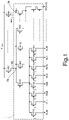
- Figure 1 shows a circuit typically used to implement the column decoder 1. Any local bitline BL is selected only when the corresponding path to V HIGH is enabled.
- PMOS transistors YO i.e., one transistor for each bit line BL
- implement a second addressing level i.e., one transistor for each bit line BL
- each transistor M can program one cell belonging to any of the associated bit lines BL.
- the row decoder selects the addressed cell by raising the corresponding word line WL to a bias voltage generated by a row voltage regulator.
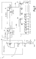
- Figure 2 shows a circuit 11 for generating a programming current for programming PCM memory cells, according to the known art.
- Circuit 11 comprises a control branch 2, including: a current generator 4, configured to cooperate to the generation of a RESET or SET pulse, depending on the operating condition, connected between a reference terminal 4a (ground, GND) and a biasing terminal 4b; and a control transistor 6 (here, a diode-connected P-type MOSFET), forming a first element of a current mirror 5.
- a current generator 4 configured to cooperate to the generation of a RESET or SET pulse, depending on the operating condition, connected between a reference terminal 4a (ground, GND) and a biasing terminal 4b
- a control transistor 6 here, a diode-connected P-type MOSFET
- the current generator 4 is, e.g., a Digital-to-analog-Converter, DAC, and is configured to generate a current pulse I DAC in the control branch 2.
- DAC Digital-to-analog-Converter
- the current generator 4 and the control transistor 6 are connected in series between the ground reference terminal 4a and a line 34 at V HIGH voltage, for example equal to 5 V.
- the control branch 2 further includes, between the current generator 4 and the transistor 6, in series to the current generator 4 and the control transistor 6, a switch 3, adapted to be switched on and off with the aim of connecting and, respectively disconnecting, the current generator 4 to, respectively from, the rest of the control branch 2 (in particular, to connect/disconnect the current generator 4 to/from the current mirror 5); the switch 28 is, e.g., a n-type MOFET device controlled by a Vdd signal generated by a control logic which is not part of the present invention.
- the Vdd signal has a value adapted to turn on the switch 3 when the memory is being programmed and to turn off the switch 3 otherwise, so that no undesired current can flow to the memory cells through the mirror 5.
- the switch 3 is optional, and may be omitted or designed in a different way.
- the control branch 2 further comprises a cascode switch 7, e.g. a n-type MOSFET device, arranged in series to the switch 3, electrically arranged between the switch 3 and the mirror device 5.
- the cascode switch 7 has a control terminal (gate) controlled by a signal Vcasc, provided by a regulator of a known type.
- the cascode switch 7 has the function of improving the electrical isolation between the part of the control branch 2 which includes the current generator 4 (low voltage portion of the branch 2, where voltage is in the range 0.5-0.9 V) and the part of the control branch 2 that includes the current mirror 5 (high voltage portion of the control branch 2, at voltage V HIGH ), so that reverse transmission is reduced as there is no direct coupling between the two portions at different voltages.
- said current I DAC flows through the control branch 2 between the line at V HIGH and the ground reference terminal GND, and is mirrored, through the current mirror 5, in respective programming currents I PROG of a plurality of main bitlines MBL 1 , ..., MBL J .
- the current I PROG (SET/RESET pulse) flows through the respective main bitline MBL 1 , ..., MBL J , depending on the activation of transistors M (here, P-type MOSFETs).
- the transistors M are connected in a current-mirror configuration to the transistor 6.
- the activation of the transistors M is controlled by two respective switches which are turned on and off by enabling signals EN_PULSE, /EN_PULSE (wherein /EN_PULSE has a logic value complementary to that of EN_PULSE).
- a switch 10 e.g., P-channel transistor
- a switch 12 e.g., P-channel transistor
- the current I DAC on the control branch 2 is mirrored in the main bitline MBL 1 only when switch 10 is turned on and, at the same time, switch 12 is turned off, i.e., only when the signals EN_PULSE and /EN_PULSE have a respective (complementary) value such as to bring the switch 10 in a conduction state and the switch 12 in interdiction.
- the programming current I PROG (SET/RESET pulse) is supplied to each phase-change memory element which must be programmed by means of this current. It is apparent that the current pulses should be shaped and have an amplitude such as to induce the phase transition in the phase change memory elements to which they are applied. Moreover, it is known to the Applicant to apply current pulses to several memory elements in parallel, to speed up the writing operation.
- the transistors M are affected by channel modulation due to the undesired variation of their drain-source voltage V DS due to an uncontrolled variation of the resistance on the main bitlines MBL 1 , ..., MBL J .
- This effect is due to the fact that the resistance of each PCM cell is not perfectly equal to the resistance of the other PCM cells, because of variations occurring during the manufacturing process and during use and, at the same time, the intensity of the programming pulses can vary unexpectedly from one cycle to another due to non-idealities.
- the voltages at nodes 8a, 9a (terminals of driving transistors M[0], ..., M[J]) of the main bitlines MBL 1 , ..., MBL J , depend unpredictably on the electrical resistance value of the phase change memory elements being programmed and on the amplitude of the current pulses applied to them.
- the channel modulation effect has an impact on current pulse amplitude precision. This means that not all the programming pulses are equally effective and suitable to set the desired resistive state (SET or RESET) to the memory element to which they are applied.
- Patent document US2008/298122 relates to a phase change memory device comprising a plurality of cells including a phase change memory element and a select device, wherein the select device is configured to cause the cells to operate during reading at a voltage and current below a level that would cause a read disturb.
- Patent document US2013/229863 relates to a driving stage for phase change non-volatile memory devices, designed for the supply of driving currents during programming operations of the memory cells.
- Patent document US2009/091969 relates to a resistance change memory, e.g., a write-system circuit of a resistance change memory.
- a current-generator circuit a device including the current-generator circuit and a system including the device are provided, as defined in the annexed claims.
- the present invention relates to a current-generator circuit operable to generate an output current pulse to be fed to a resistive load, comprising:
- the present invention will be now described with specific reference to a programming circuit adapted for generating programming current pulses suitable for programming one or more memory cells of a phase-change type, without losing generality.
- the present invention finds application as programming circuit for any kind of resistive memory (e.g., conductive bridge RAM - CBRAM, Oxide based RAM - OxRAM, etc.), as well as current generator for resistive heaters that are employed in high temperature gas sensors, for reconfigurable integrated antennas, for dispenser cathodes, for beam control in semiconductor laser, and for still other applications, devices and systems requiring a current generator which is insensitive to the effect of the resistive load.
- resistive memory e.g., conductive bridge RAM - CBRAM, Oxide based RAM - OxRAM, etc.
- current generator for resistive heaters that are employed in high temperature gas sensors, for reconfigurable integrated antennas, for dispenser cathodes, for beam control in semiconductor laser, and for still other applications, devices and systems requiring a current generator which is insensitive to the
- Figure 3 shows a programming circuit 21 for generating programming current pulses suitable for programming one or more memory cells of a phase-change type.
- the programming circuit 21 includes a compensation circuit 20 operatively coupled to the circuit 11 of Figure 2 , with the aim of compensating or reducing the channel modulation effect discussed above.
- the compensation circuit 20 includes a biasing branch 22 and a compensation branch 24; the biasing branch 22 extends between the high-voltage line 34 at voltage V HIGH (e.g., between 4 and 6 V) and the reference terminal GND at reference voltage (e.g., at 0 V).
- the biasing branch 22 is configured to generate a biasing current I bias and to mirror the biasing current I bias to the compensation branch 24 through a current mirror 23 (in particular, with unitary gain).
- the compensation branch 24 analogously extends between the high-voltage line 34 and the reference terminal GND.
- the biasing branch 22 comprises a current generator 26 (e.g., a Digital-to-analog-Converter, DAC, to allow digital current control), configured to generate a current pulse in the biasing branch 22 having an amplitude that is a fraction of the amplitude of the current pulse I DAC generated by the control branch 2 of the circuit 11 of Figure 2 .
- a current generator 26 e.g., a Digital-to-analog-Converter, DAC, to allow digital current control
- the current pulse I DAC generated by the control branch 2 has an amplitude "A”
- the current pulse I bias generated by the DAC 26 has an amplitude " ⁇ A”, with ⁇ 1 (preferably, ⁇ 1, more specifically 0.5 ⁇ 0.8).
- the biasing branch 22 is arranged in parallel to the control branch 2, between V HIGH and GND.
- Current generators 4 and 26 are chosen or manufactured or operated so that the can supply a respective current pulse I DAC and I bias having the desired ratio, as discussed above. Being the two branches 2 and 22 in parallel to one another, the choice of the respective electrical resistances or of the maximum current that can be generated by the respective current generators 4 and 26 determines the amount of actual current I DAC and I bias that can flow through the branches 2 and 22.
- the biasing branch 22 further includes a first control switch 28, adapted to be switched on and off with the aim of connecting and, respectively disconnecting, the DAC 26 to, respectively from, the rest of the biasing branch 22 (in particular, connect/disconnect the DAC 26 to/from the current mirror 23);
- the first control switch 28 is, e.g., a n-type MOFET device controlled by the Vdd signal, as discussed with reference to Figure 2 .
- the Vdd signal has a value adapted to turn on the first control switch 28 when the memory is being programmed and to turn off the first control switch 28 when no programming operation is required.
- the first control switch 28 is optional, and may be omitted.
- the biasing branch 22 further comprises a cascode switch 30, e.g. a n-type MOSFET device, arranged in series to the first control switch 28, electrically between the DAC 26 and the high-voltage line 34 (in particular, between the first control switch 28, when present, and the high-voltage line 34).
- the cascode switch 30 has a control terminal (gate) controlled by the signal V casc , provided by the regulator as already discussed with reference to Figure 2 .
- the cascode switch 30 has the function of improving the electrical isolation between the part of the biasing branch 22 which includes the DAC 26 (low voltage portion of the biasing branch 22, where voltage is in the range 0.5-0.9 V) and the part of the biasing branch 22 that includes the current mirror 23 (high voltage portion of the biasing branch 22, at voltage V HIGH in the range 4-6V), so that reverse transmission is reduced as there is no direct coupling between the two portions at different voltages.
- the current mirror 23 is formed in part by a mirror device 32 (here, a p-type MOSFET) arranged in the biasing branch 22 in series to the cascode switch 30, more specifically between the cascode switch 30 and the high-voltage line 34.
- the mirror device 32 is diode-connected, i.e. its control terminal (gate) is electrically connected to its drain terminal.
- the compensation branch 24 substantially replicates the biasing branch 22, as it comprises:
- the current mirror 23 is moreover formed in part by a second mirror device 42 (here, a p-type MOSFET), which is arranged in the compensation branch 24 in series to the cascode switch 40, more specifically between the cascode switch 40 and the high-voltage biasing line 34 at voltage V HIGH .
- the second mirror device 42 has a control terminal (gate) connected to the control terminal (gate) of the mirror device 32, thus forming the current mirror 23.
- the compensation branch 24 further comprises a resistive block 50 that mimics (in an embodiment, is equal to) the equivalent electrical resistance at node 8a, 9a of each main bitline MBL 1 , ..., MBL J during a programming step (i.e., during logic data writing in the phase-change element).
- the main source of electrical resistance is given by the series of the electrical resistance(s) of the selector device(s) of the column decoder 1 and the electrical resistance of the phase-change element of the memory cell to be addressed (i.e., to be programmed).
- the selector devices include, in particular, the transistor YM and the transistor YO which are activated (turned on) to address the PCM memory cell to be programmed, i.e. activated to connect the local bitline BL (to which the PCM memory cell to be programmed is coupled) to the main bitline MBL 1 .
- Further selector devices may be coupled to the main bitline MBL 1 and/or to the local bitline BL, according to the specific design of the memory considered.
- the resistive block 50 is designed in such a way to have an electrical resistance which is given by the sum of the electrical resistance of the phase-change memory cell during the programming step, plus any resistance introduced by the one or more selector YM, YO devices present on the path between the driving transistor and the phase-change memory cell being programmed (programming path).
- the electrical resistance R PCM is that of the phase-change material of the memory cell at its melting point.
- Resistances R YO and R YM are the resistances of the transistors YO, respectively, YM when activated (i.e., during conduction).
- a node 24a is identified in the compensation branch 24 between the cascode switch 40 and the DAC 36, more precisely between the cascode switch 40 and the second control switch 38.
- a node 2a is identified in the control branch 2 of circuit 11 between the cascode switch 7 and the current generator 4, more precisely between the cascode switch 7 and the switch 3.
- current generator 36 sinks the current I bias from branch 22 through the mirror 23, however, due to the channel modulation effect of transistor 42 caused by the difference between the drain-to-source voltages of transistor 42 and transistor 32, a current I NC ⁇ I bias flows through transistor 42.
- Current I COMP may either be a positive current that is summed to the current I DAC generated by the current generator 4, or a negative current that is subtracted from the current I DAC . Accordingly, a current I CTR flowing in the control branch 2 is given by I DAC -I COMP ; the current I CTR is mirrored through the current mirror 5 in the program current I prog .
- a voltage drop V DS_COMP on the second mirror device 43 (substantially) equals a voltage drop V DS_PROG on transistor M[0] (analogously, on transistor M[J]), and I prog ⁇ I DAC .
- the programming current I prog is no more dependent (or minimally dependent) from the resistance of the phase-change material of the memory cell being programmed, since the modulation effect on the drain-source voltage of transistors M is balanced by the compensation current I COMP .
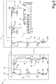
- the schematic block of Figure 4 shows a memory system 50 comprising the circuits 11 and 20 previously disclosed, and includes:
- PCM memory array 52 which contains for example 557568 memory cells divided in 528 row (WLs) and 1056 column (BLs).
- Data are stored in the memory using a differential approach and, therefore, cells are split into two categories: Direct Cells (DCs) and Complementary Cells (CCs).
- DCs Direct Cells
- CCs Complementary Cells
- the FSM 54 controls the internal operations of the memory system 50 (e.g., boot, write, read, etc.), and manages data reception and transmission through, e.g., a 32 bit Advanced High-performance Bus (AHB), which exploits a AMBA (Advanced Microcontroller Bus Architecture) protocol.
- a clock is provided to the FSM 54 by the internal oscillator 60 that is designed to work at 10 MHz and is trimmed during the EWS phase to adjust its frequency in order to attenuate the effect of process spreads.
- the FSM 54 loads the trimming configurations and the pulse settings from the memory reserved sector to the registers.
- Figure 5 illustrates a portion of an electronic system 70, which may be used in electronic devices, such as: a PDA (Personal Digital Assistant); a portable or fixed computer, possibly with wireless data-transfer capacity; a cellphone; a digital audio player; a photographic camera or video camera; a wearable electronic device; or further devices that are able to process, store, transmit and receive information.
- PDA Personal Digital Assistant
- portable or fixed computer possibly with wireless data-transfer capacity
- a cellphone a digital audio player
- a photographic camera or video camera a wearable electronic device
- wearable electronic device or further devices that are able to process, store, transmit and receive information.
- the electronic system 70 comprises a controller 71 (for example, provided with a microprocessor, a DSP, or a microcontroller), an input/output device 72 (for example, provided with a keypad and a display), for entering and displaying data, the memory system 50, a wireless interface 74, for example an antenna, for transmitting and receiving data through a radiofrequency wireless communication network and a RAM 75, all coupled through a bus 76.
- a battery 77 may be used as electric power supply source in the electronic system 70, which may further be provided with a photographic or video camera 78.
- Figure 6 shows a current-generator circuit 100 operable to generate an output current pulse I load to be fed to one or more resistive loads 102 (a plurality of resistive loads is shown in Figure 6 ). Elements which are common to the circuit of Figure 3 are apparent, and therefore reference to them may be made to better understand the following description of Figure 6 .
- the invention of Figure 6 finds application as current-generation circuit for any kind of resistive memories (e.g., conductive bridge RAM - CBRAM, Oxide based RAM - OxRAM, etc.), or as current generator for resistive heaters that are employed in high temperature gas sensors, for reconfigurable integrated antennas, for dispenser cathodes, for beam control in semiconductor laser, and for still other applications, devices and systems requiring a current generator which is insensitive to the effect of the resistive load.
- resistive memories e.g., conductive bridge RAM - CBRAM, Oxide based RAM - OxRAM, etc.
- resistive heaters that are employed in high temperature gas sensors
- reconfigurable integrated antennas for dispenser cathodes, for beam control in semiconductor laser, and for still other applications, devices and systems requiring a current generator which is insensitive to the effect of the resistive load.
- each resistive load 102 has a resistance Rioad which is approximately the same of the resistance Rioad of the other resistive loads 102.
- the current-generator circuit 100 comprises:
- the second compensation branch 116 is electrically coupled to the control branch 106 to supply the control branch 106 with the compensation current pulse I COMP in such a way that the compensation current pulse I COMP is subtracted from the control current pulse I DAC to generate a compensated current pulse I CTR .
- Each driver 110 is electrically coupled to the control branch 106 and to the respective resistive load 102 to receive from the control branch 106 the compensated current pulse I CTR and to generate the output current pulse I load as a function of the compensated current pulse I CTR .
- the first and second compensation branches 114, 116 are connected, as said, in a current mirror configuration 118, to this end, the first compensation branch 114 includes a p-channel transistor 132 having a source node, a gate node and a drain node.
- the source node is coupled to a supply voltage node V HIGH and the gate node (also referred to herein as the mirror node) is coupled to the drain node at an intermediate node 131.
- the p-channel transistor 132 is accordingly a diode-connected device.
- a current generator (or current source) 136 (e.g., a Digital-to-analog-Converter, DAC, to allow digital current control) is configured to generate the current pulse I bias in the first biasing branch 114, and accordingly is coupled between the drain node of transistor 132 and a ground reference node GND, in series to the transistor 132.
- DAC Digital-to-analog-Converter
- the second compensation branch 116 includes a p-channel transistor 142 having a source node, a gate node and a drain node.
- the source node is coupled to the supply voltage node V HIGH and the gate node is connected to the gate (mirror) node of the transistor 132, thus forming the current mirror 118.
- a current generator (current source) 138 is coupled to the drain node of transistor 142, in series connection, and to the ground reference node GND.
- the current source 138 sinks the current I DAC from the gate (mirror) node of transistor 132.
- the resistive block 120 has an electrical resistance R load ' that is a function (i.e., "mimics") of the electrical resistance R load of each of the resistive loads 102.
- the circuit 100 further includes the control branch 106, which in turn includes the current generator 108 and a control transistor 156 (here, a diode-connected P-type MOSFET).
- the current generator 108 is, e.g., a Digital-to-analog-Converter, DAC, and is configured to generate a current pulse I DAC in the control branch 106.
- the current generator 108 and the control transistor 156 are connected in series to one another, between the supply voltage node V HIGH and the ground reference node GND, in such a way that the source node of the control transistor 156 is coupled to the supply voltage node V HIGH and the drain node of the control transistor 156 is coupled to the current generator 108.
- current generator 138 sinks the current I bias from branch 114 through the mirror 118; however, due to the channel modulation effect of transistor 142 caused by the difference between the drain-to-source voltages of transistor 142 and transistor 132, a current I NC ⁇ I bias flows through transistor 142.
- Current I COMP may either be a positive current that is summed to the current I DAC generated by the current generator 108, or a negative current that is subtracted from the current I DAC . Accordingly, a current I CTR flowing in the control branch 106 is given by I DAC -I COMP .
- the circuit 100 further includes a plurality of output legs 126.
- Each output leg 126 is formed by a respective p-channel transistor 128 having a source node, a gate node and a drain node.
- the source node is coupled to the supply voltage node V HIGH and the gate node is connected to the gate node of the transistor 156 (current-mirror configuration 155) through a switch circuit 150.
- the switch circuit 150 is actuated to a closed state in response to an enable signal EN in order to enable the current mirroring operation in each output leg 126, outputting an output current I load that mirrors the control current I CTR .
- a mirroring ratio 1:G between the transistor 156 and each transistor 128 may be present (e.g., 1:10), and is defined by the difference in transistor size (width/length).
- Each electric (resistive) loads 102 is connected in series to one respective transistor 128 in the respective output leg 126.
- the output current I load is no more dependent (or minimally dependent) from the resistance R load of the loads 102.
- each of branches 114, 116 and 106 of the circuit 100 may include one or more switches (transistors) as the transistors 28, 30, 38, 40, 3, 7 previously discussed with reference to Figures 2 and 3 , according to the needs and the specific application.
- the mirroring ratio has been enhanced and a more accurate pulse shape is achieved.
- the added power consumption is negligible with respect to the power consumption of the writing pulses.
Landscapes
- Engineering & Computer Science (AREA)
- Microelectronics & Electronic Packaging (AREA)
- Physics & Mathematics (AREA)
- Chemical & Material Sciences (AREA)
- Crystallography & Structural Chemistry (AREA)
- Power Engineering (AREA)
- Nonlinear Science (AREA)
- Electromagnetism (AREA)
- General Physics & Mathematics (AREA)
- Radar, Positioning & Navigation (AREA)
- Automation & Control Theory (AREA)
- Semiconductor Memories (AREA)
- Control Of Electrical Variables (AREA)
- Control Of Eletrric Generators (AREA)
Claims (13)
- Stromgeneratorschaltung (100; 21), die funktionsfähig ist, einen Ausgangsstromimpuls (Iload; IPROG) zu erzeugen, der in eine Ausgangslast (102) durch einen Ausgangsabschnitt (126; MBLJ), mit dem die Ausgangslast (102) gekoppelt ist, eingespeist werden soll, umfassend:- eine Ausgangsstromgeneratorschaltung (104; 11), die beinhaltet:• einen Steuerzweig (106; 2), der mit einem Steuerstromgenerator (108; 4) gekoppelt ist, der konfiguriert ist, einen Steuerstromimpuls (IDAC) zu liefern, und• einen Programmtreiber (110, 128; 5, 6, M[J]), der elektrisch zwischen dem Steuerzweig (106; 2) und dem Ausgangsabschnitt (126; MBLJ) gekoppelt ist; und- eine Kompensationsschaltung (112; 20), umfassend:wobei der zweite Kompensationszweig (116; 24) elektrisch mit dem Steuerzweig (106; 2) verbunden ist, um den Steuerzweig (106; 2) mit dem Kompensationsstromimpuls (ICOMP) zu versorgen, sodass der Kompensationsstromimpuls (ICOMP) zu/von dem Steuerstromimpuls (IDAC) addiert/subtrahiert wird, um einen kompensierten Stromimpuls (ICTR) zu erzeugen,• einen ersten Kompensationszweig (114; 22), der elektrisch parallel mit dem Steuerzweig (106; 2) verbunden ist, einschließlich eines ersten Kompensationsstromgenerators (136; 26), der konfiguriert ist, einen ersten Kompensationsstromimpuls (Ibias) zu liefern, der gleich, oder ein Bruchteil (α) von, dem Steuerstromimpuls (IDAC) ist;• einen zweiten Kompensationszweig (116; 24), der elektrisch in einer Stromspiegelkonfiguration (118; 23) mit dem ersten Kompensationszweig (114; 22) zum Empfangen des ersten Kompensationsstromimpulses (Ibias) verbunden ist, einschließlich eines Widerstandsblocks (120; 50) mit einem elektrischen Widerstand (Rload'; RCOMP), der ungefähr gleich dem Widerstand (Rload) der Ausgangslast (102) ist,
und wobei der Programmtreiber (110, 128; 5, 6, M[J]) elektrisch, mittels einer Stromspiegelschaltungsanordnung mit einer Spiegelverstärkung (G), mit dem Steuerzweig (106; 2) verbunden ist und ferner elektrisch mit dem Ausgangsabschnitt (126; MBLJ) verbunden ist, um vom Steuerzweig (106; 2), durch die Stromspiegelschaltungsanordnung, den kompensierten Stromimpuls (ICTR) zu empfangen und den Programmstromimpuls (IPROG) zu liefern, der einen Wert gleich dem Wert des kompensierten Stromimpulses (ICTR) verstärkt durch die Verstärkung (G) aufweist. - Schaltung (100; 21) nach Anspruch 1, wobei die Stromspiegelschaltungsanordnung (155; 5) einen ersten Spiegeltransistor (156; 6) beinhaltet, der in einer Stromspiegelkonfiguration mit einem zweiten Spiegeltransistor (128; M[J]) verbunden ist,
und wobei der erste Spiegeltransistor (156; 6) mit dem Steuerstromgenerator (108; 4) gekoppelt ist und der zweite Spiegeltransistor (128; M[J]) mit dem Ausgangsabschnitt (126; MBLJ) gekoppelt ist, sodass der Programmstromimpuls (Iprog) eine Kopie, verstärkt durch die Verstärkung (G), des kompensierten Stromimpulses (ICTR) ist. - Schaltung (100; 21) nach Anspruch 1 oder Anspruch 2, wobei der erste Kompensationszweig (114; 22) zwischen einer Biasing-Leitung (34) bei einer ersten Spannung (VHIGH) und einer Referenzleitung (GND) bei einer zweiten Spannung, die geringer als die erste Spannung ist, gekoppelt ist und beinhaltet: Den ersten Kompensationsstromgenerator (136; 26), der elektrisch mit der Referenzleitung (GND) gekoppelt ist; einen ersten Kaskodentransistor (30), der elektrisch zwischen dem ersten Kompensationsstromgenerator (136; 26) und der Biasing-Leitung (34) gekoppelt ist; und einen dritten Spiegeltransistor (132; 32), der elektrisch zwischen dem ersten Kaskodentransistor (30) und der Biasing-Leitung (34) gekoppelt ist,und wobei der zweite Kompensationszweig (116; 24) zwischen der Biasing-Leitung (34) und der Referenzleitung (GND) gekoppelt ist und beinhaltet: Einen zweiten Kompensationsstromgenerator (138; 36), der elektrisch mit der Referenzleitung (GND) gekoppelt und konfiguriert ist, den ersten Kompensationsstromimpuls (Ibias) zu erzeugen; einen zweiten Kaskodentransistor (40), der elektrisch zwischen dem zweiten Kompensationsstromgenerator (36) und der Biasing-Leitung (34) gekoppelt ist; und einen vierten Spiegeltransistor (142; 42), der elektrisch zwischen dem zweiten Kaskodentransistor (40) und der Biasing-Leitung (34) gekoppelt ist,wobei der dritte und vierte Spiegeltransistor (132, 142; 32, 42) miteinander gemäß der Stromspiegelkonfiguration (118; 23) verbunden sind, um den ersten Kompensationsstromimpuls (Ibias) vom ersten Kompensationszweig (114; 22) zu versenken.
- Schaltung (100; 21) nach den Ansprüchen 2 und 3, wobei der Steuerzweig (106; 2) einen dritten Kaskodentransistor (7) umfasst, der elektrisch in Reihe mit, und zwischen, dem ersten Spiegeltransistor (156; 6) und dem Steuerstromgenerator (108; 4) gekoppelt ist,
wobei ein erster Knoten (124a; 24a) zwischen dem zweiten Kaskodentransistor (40) und dem zweiten Kompensationsstromgenerator (138; 36) definiert ist und ein zweiter Knoten (124b; 2a) zwischen dem dritten Kaskodentransistor (7) und dem Steuerstromgenerator (108; 4) definiert ist, wobei der erste und der zweite Knoten (124a, 124b; 24a, 2a) miteinander kurzgeschlossen werden, um den Kompensationsstromimpuls (ICOMP) vom zweiten Kompensationszweig (116; 24) zu dem Steuerzweig (106; 2) zu liefern. - Schaltung (100; 21) nach Anspruch 3 oder 4, wobei der Widerstandsblock (120; 50) elektrisch in Reihe mit, und zwischen, dem vierten Spiegeltransistor (142; 42) und dem zweiten Kaskodentransistor (40) gekoppelt ist.
- Schaltung (100; 21) nach einem der vorstehenden Ansprüche, wobei der Ausgangsabschnitt (126; MBLJ) mit einem Spaltendecodierer (1) eines Speicherarrays gekoppelt ist, das mindestens eine Bitleitung (BL) beinhaltet, mit der eine Phasenwechselspeicherzelle, die durch den Programmstromimpuls (IPROG) programmiert werden soll, gekoppelt ist,
wobei der Spaltendecodierer (1) eine oder mehrere Selektorvorrichtungen (YM, YO) beinhaltet, die funktionsfähig sind, die Bitleitung (BL) zu adressieren, und wobei der Widerstandsblock (50) einen elektrischen Widerstand (Rload'; RCOMP) aufweist, der eine Funktion des Widerstands der Phasenwechselspeicherzelle während einer Programmieroperation der Phasenwechselspeicherzelle ist. - Programmierschaltung (100; 21) nach Anspruch 6, wobei der Widerstandsblock (50) einen elektrischen Widerstand (RCOMP) aufweist, der darüber hinaus eine Funktion des elektrischen Widerstands der einen oder der mehreren Selektorvorrichtungen (YM, YO) auf eine solche Weise ist, dass der elektrische Widerstand (RCOMP) des Widerstandsblocks (50) durch die Summe der elektrischen Widerstände der einen oder der mehreren Selektorvorrichtungen (YM, YO) und der Phasenwechselspeicherzelle während der Programmieroperation gegeben ist.
- Schaltung (100; 21) nach Anspruch 6 oder 7, wobei der elektrische Widerstand der Phasenwechselspeicherzelle während der Programmieroperation der elektrische Widerstand des Phasenwechselmaterials der Phasenwechselspeicherzelle bei seinem Schmelzpunkt ist.
- Phasenwechselspeichervorrichtung (50), umfassend:- ein Speicherarray (52), das mit einer Vielzahl von Lokalbitleitungen (BL) versehen ist, die mit jeweiligen Speicherzellen verbunden sind, die jeweilige logische Daten speichern;- einen Spaltendecodierer (1), der mit dem Speicherarray gekoppelt ist, zum Adressieren einer Lokalbitleitung (BL), die mit einer Speicherzelle verbunden ist, die programmiert werden muss;- eine Stromgeneratorschaltung (100; 21) nach einem der Ansprüche 1-8, die über den Spaltendecodierer (1) mit dem Speicherarray gekoppelt ist, zum Schreiben logischer Daten in die Speicherzelle, die mit der adressierten Lokalbitleitung (BL) verbunden ist.
- Phasenwechselspeichervorrichtung nach Anspruch 9, ferner umfassend mindestens eine Hauptbitleitung (MBLJ), die die Programmierschaltung (21) mit der adressierten Lokalbitleitung (BL) verbindet; und- eine oder mehrere Selektorvorrichtungen (YM, YO), die mit der adressierten Lokalbitleitung (BL) gekoppelt und funktionsfähig sind, die adressierte Lokalbitleitung (BL) elektrisch mit der Hauptbitleitung (MBLJ) zu verbinden, um einen elektrischen Pfad zwischen der zu beschreibenden Speicherzelle und der Hauptbitleitung (MBLJ) einzurichten.
- Elektronische Vorrichtung, die eine Stromgeneratorschaltung (100; 21) nach einem der Ansprüche 1-8 beinhaltet.
- Elektronische Vorrichtung nach Anspruch 11, die gewählt wird aus: Einem Widerstandsspeicher, einer Widerstandsheizvorrichtung, einer rekonfigurierbaren integrierten Antenne, einer Vorratskathode, einer Strahlsteuerung für einen Halbleiterlaser.
- System (70), das eine Phasenwechselspeichervorrichtung nach Anspruch 9 oder 10 und/oder eine elektronische Vorrichtung nach Anspruch 11 oder 12 umfasst, die gewählt wird aus: Einem PDA (Personal Digital Assistant); einem portablen Computer; einem Mobiltelefon; einem digitalen Audioplayer; einer fotografischen Kamera oder Videokamera; einer tragbaren elektronischen Vorrichtung; einer portablen elektronischen Vorrichtung; einem Halbleiterlaser; einem Hochtemperatur-Gassensor; einer Sensorvorrichtung.
Applications Claiming Priority (1)
| Application Number | Priority Date | Filing Date | Title |
|---|---|---|---|
| IT102019000013695A IT201900013695A1 (it) | 2019-08-01 | 2019-08-01 | Circuito generatore di corrente, dispositivo includente il circuito generatore di corrente e sistema elettronico |
Publications (2)
| Publication Number | Publication Date |
|---|---|
| EP3772061A1 EP3772061A1 (de) | 2021-02-03 |
| EP3772061B1 true EP3772061B1 (de) | 2022-11-02 |
Family
ID=68653544
Family Applications (1)
| Application Number | Title | Priority Date | Filing Date |
|---|---|---|---|
| EP20188675.1A Active EP3772061B1 (de) | 2019-08-01 | 2020-07-30 | Stromgeneratorschaltung, vorrichtung mit der stromgeneratorschaltung und elektronisches system |
Country Status (4)
| Country | Link |
|---|---|
| US (1) | US11189343B2 (de) |
| EP (1) | EP3772061B1 (de) |
| CN (2) | CN212724728U (de) |
| IT (1) | IT201900013695A1 (de) |
Families Citing this family (5)
| Publication number | Priority date | Publication date | Assignee | Title |
|---|---|---|---|---|
| IT201900013695A1 (it) * | 2019-08-01 | 2021-02-01 | St Microelectronics Srl | Circuito generatore di corrente, dispositivo includente il circuito generatore di corrente e sistema elettronico |
| US11335401B1 (en) * | 2021-01-28 | 2022-05-17 | National Tsing Hua University | Memory unit with multiple word lines for nonvolatile computing-in-memory applications and current calibrating method thereof |
| US11615820B1 (en) | 2021-09-30 | 2023-03-28 | Stmicroelectronics S.R.L. | Regulator of a sense amplifier |
| CN114625207A (zh) * | 2022-03-21 | 2022-06-14 | 四川创安微电子有限公司 | 一种dac电路及其增益调整方法 |
| US12512155B2 (en) * | 2022-03-24 | 2025-12-30 | Intel Corporation | Technologies for current biasing for three-dimensional crosspoint memory cells |
Family Cites Families (9)
| Publication number | Priority date | Publication date | Assignee | Title |
|---|---|---|---|---|
| US7570524B2 (en) * | 2005-03-30 | 2009-08-04 | Ovonyx, Inc. | Circuitry for reading phase change memory cells having a clamping circuit |
| US7848138B2 (en) * | 2007-06-01 | 2010-12-07 | Intel Corporation | Biasing a phase change memory device |
| JP5002401B2 (ja) * | 2007-10-03 | 2012-08-15 | 株式会社東芝 | 抵抗変化メモリ |
| ITTO20120189A1 (it) * | 2012-03-02 | 2013-09-03 | St Microelectronics Srl | Stadio di pilotaggio ad elevata efficienza per dispositivi di memoria non volatile a cambiamento di fase |
| KR20160016386A (ko) * | 2014-08-05 | 2016-02-15 | 에스케이하이닉스 주식회사 | 라이트 드라이버, 이를 포함하는 저항변화 메모리 장치 및 동작 방법 |
| ITUB20153221A1 (it) * | 2015-08-25 | 2017-02-25 | St Microelectronics Srl | Circuito e metodo di polarizzazione di celle di memoria non volatile |
| KR102476770B1 (ko) * | 2016-04-08 | 2022-12-13 | 에스케이하이닉스 주식회사 | 전자 장치 |
| US9728231B1 (en) * | 2016-05-03 | 2017-08-08 | Taiwan Semiconductor Manufacturing Co., Ltd. | Device and method for data-writing |
| IT201900013695A1 (it) * | 2019-08-01 | 2021-02-01 | St Microelectronics Srl | Circuito generatore di corrente, dispositivo includente il circuito generatore di corrente e sistema elettronico |
-
2019
- 2019-08-01 IT IT102019000013695A patent/IT201900013695A1/it unknown
-
2020
- 2020-07-28 US US16/940,837 patent/US11189343B2/en active Active
- 2020-07-30 EP EP20188675.1A patent/EP3772061B1/de active Active
- 2020-07-31 CN CN202021566046.7U patent/CN212724728U/zh not_active Withdrawn - After Issue
- 2020-07-31 CN CN202010762689.7A patent/CN112309467B/zh active Active
Also Published As
| Publication number | Publication date |
|---|---|
| US20210035637A1 (en) | 2021-02-04 |
| IT201900013695A1 (it) | 2021-02-01 |
| CN212724728U (zh) | 2021-03-16 |
| US11189343B2 (en) | 2021-11-30 |
| EP3772061A1 (de) | 2021-02-03 |
| CN112309467A (zh) | 2021-02-02 |
| CN112309467B (zh) | 2025-07-08 |
Similar Documents
| Publication | Publication Date | Title |
|---|---|---|
| EP3772061B1 (de) | Stromgeneratorschaltung, vorrichtung mit der stromgeneratorschaltung und elektronisches system | |
| US20050117388A1 (en) | Write driver circuit in phase change memory device and method for applying write current | |
| EP2159800B1 (de) | Zeilendekodierer für nicht flüchtige Speicher des Phasen-Übergangstyps | |
| US8264872B2 (en) | Column decoder for non-volatile memory devices, in particular of the phase-change type | |
| CN112216326B (zh) | 具有供电电压调节电路的相变存储器 | |
| JP2010067332A (ja) | 相補型相変化メモリセル及びメモリ回路 | |
| US11322201B2 (en) | Bit-line voltage generation circuit for a non-volatile memory device and corresponding method | |
| US8325514B2 (en) | Phase change memory device | |
| US10186317B2 (en) | Phase change memory device and method of operation | |
| EP3758000B1 (de) | Verfahren zum programmieren einer phasenwechsel-speichervorrichtung vom differentialtyp, speichervorrichtung und elektronisches system | |
| US8134858B2 (en) | Semiconductor device for supplying stable voltage to control electrode of transistor | |
| US11756614B2 (en) | Phase change memory device, system including the memory device, and method for operating the memory device | |
| EP3817001B1 (de) | Verfahren zur programmierung einer differentiellen phasenänderungsspeicheranordnung, phasenänderungsspeicheranordnung und elektronisches system | |
| US8264871B2 (en) | Phase change memory device | |
| US20180122470A1 (en) | Non-volatile memory, system including the memory and method for controlling the memory |
Legal Events
| Date | Code | Title | Description |
|---|---|---|---|
| PUAI | Public reference made under article 153(3) epc to a published international application that has entered the european phase |
Free format text: ORIGINAL CODE: 0009012 |
|
| STAA | Information on the status of an ep patent application or granted ep patent |
Free format text: STATUS: THE APPLICATION HAS BEEN PUBLISHED |
|
| AK | Designated contracting states |
Kind code of ref document: A1 Designated state(s): AL AT BE BG CH CY CZ DE DK EE ES FI FR GB GR HR HU IE IS IT LI LT LU LV MC MK MT NL NO PL PT RO RS SE SI SK SM TR |
|
| AX | Request for extension of the european patent |
Extension state: BA ME |
|
| STAA | Information on the status of an ep patent application or granted ep patent |
Free format text: STATUS: REQUEST FOR EXAMINATION WAS MADE |
|
| 17P | Request for examination filed |
Effective date: 20210728 |
|
| RBV | Designated contracting states (corrected) |
Designated state(s): AL AT BE BG CH CY CZ DE DK EE ES FI FR GB GR HR HU IE IS IT LI LT LU LV MC MK MT NL NO PL PT RO RS SE SI SK SM TR |
|
| GRAP | Despatch of communication of intention to grant a patent |
Free format text: ORIGINAL CODE: EPIDOSNIGR1 |
|
| STAA | Information on the status of an ep patent application or granted ep patent |
Free format text: STATUS: GRANT OF PATENT IS INTENDED |
|
| INTG | Intention to grant announced |
Effective date: 20220527 |
|
| GRAS | Grant fee paid |
Free format text: ORIGINAL CODE: EPIDOSNIGR3 |
|
| GRAA | (expected) grant |
Free format text: ORIGINAL CODE: 0009210 |
|
| STAA | Information on the status of an ep patent application or granted ep patent |
Free format text: STATUS: THE PATENT HAS BEEN GRANTED |
|
| AK | Designated contracting states |
Kind code of ref document: B1 Designated state(s): AL AT BE BG CH CY CZ DE DK EE ES FI FR GB GR HR HU IE IS IT LI LT LU LV MC MK MT NL NO PL PT RO RS SE SI SK SM TR |
|
| REG | Reference to a national code |
Ref country code: GB Ref legal event code: FG4D |
|
| REG | Reference to a national code |
Ref country code: CH Ref legal event code: EP Ref country code: AT Ref legal event code: REF Ref document number: 1529365 Country of ref document: AT Kind code of ref document: T Effective date: 20221115 |
|
| REG | Reference to a national code |
Ref country code: DE Ref legal event code: R096 Ref document number: 602020006000 Country of ref document: DE |
|
| REG | Reference to a national code |
Ref country code: IE Ref legal event code: FG4D |
|
| REG | Reference to a national code |
Ref country code: LT Ref legal event code: MG9D |
|
| REG | Reference to a national code |
Ref country code: NL Ref legal event code: MP Effective date: 20221102 |
|
| REG | Reference to a national code |
Ref country code: AT Ref legal event code: MK05 Ref document number: 1529365 Country of ref document: AT Kind code of ref document: T Effective date: 20221102 |
|
| PG25 | Lapsed in a contracting state [announced via postgrant information from national office to epo] |
Ref country code: SE Free format text: LAPSE BECAUSE OF FAILURE TO SUBMIT A TRANSLATION OF THE DESCRIPTION OR TO PAY THE FEE WITHIN THE PRESCRIBED TIME-LIMIT Effective date: 20221102 Ref country code: PT Free format text: LAPSE BECAUSE OF FAILURE TO SUBMIT A TRANSLATION OF THE DESCRIPTION OR TO PAY THE FEE WITHIN THE PRESCRIBED TIME-LIMIT Effective date: 20230302 Ref country code: NO Free format text: LAPSE BECAUSE OF FAILURE TO SUBMIT A TRANSLATION OF THE DESCRIPTION OR TO PAY THE FEE WITHIN THE PRESCRIBED TIME-LIMIT Effective date: 20230202 Ref country code: LT Free format text: LAPSE BECAUSE OF FAILURE TO SUBMIT A TRANSLATION OF THE DESCRIPTION OR TO PAY THE FEE WITHIN THE PRESCRIBED TIME-LIMIT Effective date: 20221102 Ref country code: FI Free format text: LAPSE BECAUSE OF FAILURE TO SUBMIT A TRANSLATION OF THE DESCRIPTION OR TO PAY THE FEE WITHIN THE PRESCRIBED TIME-LIMIT Effective date: 20221102 Ref country code: ES Free format text: LAPSE BECAUSE OF FAILURE TO SUBMIT A TRANSLATION OF THE DESCRIPTION OR TO PAY THE FEE WITHIN THE PRESCRIBED TIME-LIMIT Effective date: 20221102 Ref country code: AT Free format text: LAPSE BECAUSE OF FAILURE TO SUBMIT A TRANSLATION OF THE DESCRIPTION OR TO PAY THE FEE WITHIN THE PRESCRIBED TIME-LIMIT Effective date: 20221102 |
|
| PG25 | Lapsed in a contracting state [announced via postgrant information from national office to epo] |
Ref country code: RS Free format text: LAPSE BECAUSE OF FAILURE TO SUBMIT A TRANSLATION OF THE DESCRIPTION OR TO PAY THE FEE WITHIN THE PRESCRIBED TIME-LIMIT Effective date: 20221102 Ref country code: PL Free format text: LAPSE BECAUSE OF FAILURE TO SUBMIT A TRANSLATION OF THE DESCRIPTION OR TO PAY THE FEE WITHIN THE PRESCRIBED TIME-LIMIT Effective date: 20221102 Ref country code: LV Free format text: LAPSE BECAUSE OF FAILURE TO SUBMIT A TRANSLATION OF THE DESCRIPTION OR TO PAY THE FEE WITHIN THE PRESCRIBED TIME-LIMIT Effective date: 20221102 Ref country code: IS Free format text: LAPSE BECAUSE OF FAILURE TO SUBMIT A TRANSLATION OF THE DESCRIPTION OR TO PAY THE FEE WITHIN THE PRESCRIBED TIME-LIMIT Effective date: 20230302 Ref country code: HR Free format text: LAPSE BECAUSE OF FAILURE TO SUBMIT A TRANSLATION OF THE DESCRIPTION OR TO PAY THE FEE WITHIN THE PRESCRIBED TIME-LIMIT Effective date: 20221102 Ref country code: GR Free format text: LAPSE BECAUSE OF FAILURE TO SUBMIT A TRANSLATION OF THE DESCRIPTION OR TO PAY THE FEE WITHIN THE PRESCRIBED TIME-LIMIT Effective date: 20230203 |
|
| PG25 | Lapsed in a contracting state [announced via postgrant information from national office to epo] |
Ref country code: NL Free format text: LAPSE BECAUSE OF FAILURE TO SUBMIT A TRANSLATION OF THE DESCRIPTION OR TO PAY THE FEE WITHIN THE PRESCRIBED TIME-LIMIT Effective date: 20221102 |
|
| PG25 | Lapsed in a contracting state [announced via postgrant information from national office to epo] |
Ref country code: SM Free format text: LAPSE BECAUSE OF FAILURE TO SUBMIT A TRANSLATION OF THE DESCRIPTION OR TO PAY THE FEE WITHIN THE PRESCRIBED TIME-LIMIT Effective date: 20221102 Ref country code: RO Free format text: LAPSE BECAUSE OF FAILURE TO SUBMIT A TRANSLATION OF THE DESCRIPTION OR TO PAY THE FEE WITHIN THE PRESCRIBED TIME-LIMIT Effective date: 20221102 Ref country code: EE Free format text: LAPSE BECAUSE OF FAILURE TO SUBMIT A TRANSLATION OF THE DESCRIPTION OR TO PAY THE FEE WITHIN THE PRESCRIBED TIME-LIMIT Effective date: 20221102 Ref country code: DK Free format text: LAPSE BECAUSE OF FAILURE TO SUBMIT A TRANSLATION OF THE DESCRIPTION OR TO PAY THE FEE WITHIN THE PRESCRIBED TIME-LIMIT Effective date: 20221102 Ref country code: CZ Free format text: LAPSE BECAUSE OF FAILURE TO SUBMIT A TRANSLATION OF THE DESCRIPTION OR TO PAY THE FEE WITHIN THE PRESCRIBED TIME-LIMIT Effective date: 20221102 |
|
| REG | Reference to a national code |
Ref country code: DE Ref legal event code: R097 Ref document number: 602020006000 Country of ref document: DE |
|
| PG25 | Lapsed in a contracting state [announced via postgrant information from national office to epo] |
Ref country code: SK Free format text: LAPSE BECAUSE OF FAILURE TO SUBMIT A TRANSLATION OF THE DESCRIPTION OR TO PAY THE FEE WITHIN THE PRESCRIBED TIME-LIMIT Effective date: 20221102 Ref country code: AL Free format text: LAPSE BECAUSE OF FAILURE TO SUBMIT A TRANSLATION OF THE DESCRIPTION OR TO PAY THE FEE WITHIN THE PRESCRIBED TIME-LIMIT Effective date: 20221102 |
|
| PLBE | No opposition filed within time limit |
Free format text: ORIGINAL CODE: 0009261 |
|
| STAA | Information on the status of an ep patent application or granted ep patent |
Free format text: STATUS: NO OPPOSITION FILED WITHIN TIME LIMIT |
|
| 26N | No opposition filed |
Effective date: 20230803 |
|
| PG25 | Lapsed in a contracting state [announced via postgrant information from national office to epo] |
Ref country code: SI Free format text: LAPSE BECAUSE OF FAILURE TO SUBMIT A TRANSLATION OF THE DESCRIPTION OR TO PAY THE FEE WITHIN THE PRESCRIBED TIME-LIMIT Effective date: 20221102 |
|
| PG25 | Lapsed in a contracting state [announced via postgrant information from national office to epo] |
Ref country code: MC Free format text: LAPSE BECAUSE OF FAILURE TO SUBMIT A TRANSLATION OF THE DESCRIPTION OR TO PAY THE FEE WITHIN THE PRESCRIBED TIME-LIMIT Effective date: 20221102 |
|
| PG25 | Lapsed in a contracting state [announced via postgrant information from national office to epo] |
Ref country code: MC Free format text: LAPSE BECAUSE OF FAILURE TO SUBMIT A TRANSLATION OF THE DESCRIPTION OR TO PAY THE FEE WITHIN THE PRESCRIBED TIME-LIMIT Effective date: 20221102 |
|
| REG | Reference to a national code |
Ref country code: CH Ref legal event code: PL |
|
| REG | Reference to a national code |
Ref country code: BE Ref legal event code: MM Effective date: 20230731 |
|
| PG25 | Lapsed in a contracting state [announced via postgrant information from national office to epo] |
Ref country code: LU Free format text: LAPSE BECAUSE OF NON-PAYMENT OF DUE FEES Effective date: 20230730 |
|
| PG25 | Lapsed in a contracting state [announced via postgrant information from national office to epo] |
Ref country code: LU Free format text: LAPSE BECAUSE OF NON-PAYMENT OF DUE FEES Effective date: 20230730 |
|
| REG | Reference to a national code |
Ref country code: IE Ref legal event code: MM4A |
|
| PG25 | Lapsed in a contracting state [announced via postgrant information from national office to epo] |
Ref country code: CH Free format text: LAPSE BECAUSE OF NON-PAYMENT OF DUE FEES Effective date: 20230731 |
|
| PG25 | Lapsed in a contracting state [announced via postgrant information from national office to epo] |
Ref country code: IT Free format text: LAPSE BECAUSE OF FAILURE TO SUBMIT A TRANSLATION OF THE DESCRIPTION OR TO PAY THE FEE WITHIN THE PRESCRIBED TIME-LIMIT Effective date: 20221102 Ref country code: BE Free format text: LAPSE BECAUSE OF NON-PAYMENT OF DUE FEES Effective date: 20230731 Ref country code: FR Free format text: LAPSE BECAUSE OF NON-PAYMENT OF DUE FEES Effective date: 20230731 |
|
| PG25 | Lapsed in a contracting state [announced via postgrant information from national office to epo] |
Ref country code: IE Free format text: LAPSE BECAUSE OF NON-PAYMENT OF DUE FEES Effective date: 20230730 |
|
| PG25 | Lapsed in a contracting state [announced via postgrant information from national office to epo] |
Ref country code: IE Free format text: LAPSE BECAUSE OF NON-PAYMENT OF DUE FEES Effective date: 20230730 |
|
| PG25 | Lapsed in a contracting state [announced via postgrant information from national office to epo] |
Ref country code: BG Free format text: LAPSE BECAUSE OF FAILURE TO SUBMIT A TRANSLATION OF THE DESCRIPTION OR TO PAY THE FEE WITHIN THE PRESCRIBED TIME-LIMIT Effective date: 20221102 |
|
| PG25 | Lapsed in a contracting state [announced via postgrant information from national office to epo] |
Ref country code: BG Free format text: LAPSE BECAUSE OF FAILURE TO SUBMIT A TRANSLATION OF THE DESCRIPTION OR TO PAY THE FEE WITHIN THE PRESCRIBED TIME-LIMIT Effective date: 20221102 |
|
| GBPC | Gb: european patent ceased through non-payment of renewal fee |
Effective date: 20240730 |
|
| PG25 | Lapsed in a contracting state [announced via postgrant information from national office to epo] |
Ref country code: GB Free format text: LAPSE BECAUSE OF NON-PAYMENT OF DUE FEES Effective date: 20240730 |
|
| PG25 | Lapsed in a contracting state [announced via postgrant information from national office to epo] |
Ref country code: CY Free format text: LAPSE BECAUSE OF FAILURE TO SUBMIT A TRANSLATION OF THE DESCRIPTION OR TO PAY THE FEE WITHIN THE PRESCRIBED TIME-LIMIT; INVALID AB INITIO Effective date: 20200730 |
|
| PG25 | Lapsed in a contracting state [announced via postgrant information from national office to epo] |
Ref country code: HU Free format text: LAPSE BECAUSE OF FAILURE TO SUBMIT A TRANSLATION OF THE DESCRIPTION OR TO PAY THE FEE WITHIN THE PRESCRIBED TIME-LIMIT; INVALID AB INITIO Effective date: 20200730 |
|
| PGFP | Annual fee paid to national office [announced via postgrant information from national office to epo] |
Ref country code: DE Payment date: 20250620 Year of fee payment: 6 |
|
| PG25 | Lapsed in a contracting state [announced via postgrant information from national office to epo] |
Ref country code: TR Free format text: LAPSE BECAUSE OF FAILURE TO SUBMIT A TRANSLATION OF THE DESCRIPTION OR TO PAY THE FEE WITHIN THE PRESCRIBED TIME-LIMIT Effective date: 20221102 |