EP3772114B1 - Composant piézoélectrique et son procédé de fabrication - Google Patents
Composant piézoélectrique et son procédé de fabrication Download PDFInfo
- Publication number
- EP3772114B1 EP3772114B1 EP20188609.0A EP20188609A EP3772114B1 EP 3772114 B1 EP3772114 B1 EP 3772114B1 EP 20188609 A EP20188609 A EP 20188609A EP 3772114 B1 EP3772114 B1 EP 3772114B1
- Authority
- EP
- European Patent Office
- Prior art keywords
- film
- knn
- layer
- piezoelectric
- lno
- Prior art date
- Legal status (The legal status is an assumption and is not a legal conclusion. Google has not performed a legal analysis and makes no representation as to the accuracy of the status listed.)
- Active
Links
Images

Classifications
-
- H—ELECTRICITY
- H10—SEMICONDUCTOR DEVICES; ELECTRIC SOLID-STATE DEVICES NOT OTHERWISE PROVIDED FOR
- H10N—ELECTRIC SOLID-STATE DEVICES NOT OTHERWISE PROVIDED FOR
- H10N30/00—Piezoelectric or electrostrictive devices
- H10N30/80—Constructional details
- H10N30/85—Piezoelectric or electrostrictive active materials
- H10N30/853—Ceramic compositions
- H10N30/8542—Alkali metal based oxides, e.g. lithium, sodium or potassium niobates
-
- H—ELECTRICITY
- H10—SEMICONDUCTOR DEVICES; ELECTRIC SOLID-STATE DEVICES NOT OTHERWISE PROVIDED FOR
- H10N—ELECTRIC SOLID-STATE DEVICES NOT OTHERWISE PROVIDED FOR
- H10N30/00—Piezoelectric or electrostrictive devices
- H10N30/704—Piezoelectric or electrostrictive devices based on piezoelectric or electrostrictive films or coatings
- H10N30/706—Piezoelectric or electrostrictive devices based on piezoelectric or electrostrictive films or coatings characterised by the underlying bases, e.g. substrates
- H10N30/708—Intermediate layers, e.g. barrier, adhesion or growth control buffer layers
-
- H—ELECTRICITY
- H10—SEMICONDUCTOR DEVICES; ELECTRIC SOLID-STATE DEVICES NOT OTHERWISE PROVIDED FOR
- H10N—ELECTRIC SOLID-STATE DEVICES NOT OTHERWISE PROVIDED FOR
- H10N30/00—Piezoelectric or electrostrictive devices
- H10N30/01—Manufacture or treatment
- H10N30/05—Manufacture of multilayered piezoelectric or electrostrictive devices, or parts thereof, e.g. by stacking piezoelectric bodies and electrodes
-
- H—ELECTRICITY
- H10—SEMICONDUCTOR DEVICES; ELECTRIC SOLID-STATE DEVICES NOT OTHERWISE PROVIDED FOR
- H10N—ELECTRIC SOLID-STATE DEVICES NOT OTHERWISE PROVIDED FOR
- H10N30/00—Piezoelectric or electrostrictive devices
- H10N30/01—Manufacture or treatment
- H10N30/07—Forming of piezoelectric or electrostrictive parts or bodies on an electrical element or another base
- H10N30/074—Forming of piezoelectric or electrostrictive parts or bodies on an electrical element or another base by depositing piezoelectric or electrostrictive layers, e.g. aerosol or screen printing
- H10N30/076—Forming of piezoelectric or electrostrictive parts or bodies on an electrical element or another base by depositing piezoelectric or electrostrictive layers, e.g. aerosol or screen printing by vapour phase deposition
-
- H—ELECTRICITY
- H10—SEMICONDUCTOR DEVICES; ELECTRIC SOLID-STATE DEVICES NOT OTHERWISE PROVIDED FOR
- H10N—ELECTRIC SOLID-STATE DEVICES NOT OTHERWISE PROVIDED FOR
- H10N30/00—Piezoelectric or electrostrictive devices
- H10N30/01—Manufacture or treatment
- H10N30/07—Forming of piezoelectric or electrostrictive parts or bodies on an electrical element or another base
- H10N30/074—Forming of piezoelectric or electrostrictive parts or bodies on an electrical element or another base by depositing piezoelectric or electrostrictive layers, e.g. aerosol or screen printing
- H10N30/079—Forming of piezoelectric or electrostrictive parts or bodies on an electrical element or another base by depositing piezoelectric or electrostrictive layers, e.g. aerosol or screen printing using intermediate layers, e.g. for growth control
-
- H—ELECTRICITY
- H10—SEMICONDUCTOR DEVICES; ELECTRIC SOLID-STATE DEVICES NOT OTHERWISE PROVIDED FOR
- H10N—ELECTRIC SOLID-STATE DEVICES NOT OTHERWISE PROVIDED FOR
- H10N30/00—Piezoelectric or electrostrictive devices
- H10N30/80—Constructional details
- H10N30/87—Electrodes or interconnections, e.g. leads or terminals
- H10N30/871—Single-layered electrodes of multilayer piezoelectric or electrostrictive devices, e.g. internal electrodes
Definitions
- the present disclosure relates to a piezoelectric laminate, a piezoelectric element, and a method of manufacturing a piezoelectric laminate.
- a piezoelectric material is utilized widely for a functional electronic component such as a sensor and an actuator.
- Lead-based materials in particular, PZT-based ferroelectrics represented by a composition formula of Pb(Zr 1-x Ti x )O 3 are used widely for the piezoelectric material. Since PZT-based piezoelectric material includes lead, it is not preferable from a viewpoint of a pollution prevention and the like. Therefore, potassium sodium niobate (KNN) is suggested as a piezoelectric material not including lead (see patent documents 1 and 2, for example). Recently, it is strongly required to further improve a performance of the piezoelectric material configured by the material not including lead such as KNN.
- KNN potassium sodium niobate
- Patent document 3 relates to a piezoelectric device comprising a piezoelectric film having a columnar structure; and electrodes disposed in contact with the piezoelectric film, wherein the piezoelectric film has a composition containing an element which can substitute Nb and has an oxidation number of 2 or more and less than 5 when oxidized the element being in a proportion of 3.3 mol or less relative to 100 mol of potassium sodium niobate represented by a general formula (K 1-x Na x )NbO 3 , where 0 ⁇ x ⁇ 1.
- Patent document 4 concerns a piezoelectric element characterized by comprising a first electrode layer, a second electrode layer, and a piezoelectric layer sandwiched between the first electrode layer and the second electrode layer, wherein the piezoelectric layer is provided with at least one layer, each of a first piezoelectric layer which is a potassium-sodium niobate thin film substantially not containing Mn (manganese) and a second piezoelectric layer which is a potassium-sodium niobate thin film containing Mn.
- Patent document 5 describes a laminated substrate with a piezoelectric thin film, comprising a substrate; an electrode film formed on the substrate; and a piezoelectric thin film formed on the electrode film, wherein the piezoelectric thin film is made of an alkali niobium oxide represented by a composition formula of (K 1-x Na x )NbO 3 (0 ⁇ x ⁇ 1), having a perovskite structure, and oriented preferentially in (001) plane direction, and contains a metallic element selected from a group consisting of Mn and Cu at a concentration of 0.2 at% or more and 0.6 at% or less.
- an alkali niobium oxide represented by a composition formula of (K 1-x Na x )NbO 3 (0 ⁇ x ⁇ 1), having a perovskite structure, and oriented preferentially in (001) plane direction, and contains a metallic element selected from a group consisting of Mn and Cu at a concentration of 0.2 at% or more and
- An object of the present disclosure is to further improve an insulation property of a piezoelectric laminate having a piezoelectric film comprised of alkali niobium oxide.
- a piezoelectric laminate and a manufacturing method thereof according to independent claims 1 and 5, respectively.
- the present invention furthermore relates to a piezoelectric element as set out in claim 4.
- an insulation property of a piezoelectric laminate having a piezoelectric film comprised of alkali niobium oxide can be further improved.
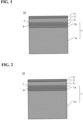
- a laminate (laminated substrate) 10 (also referred to as piezoelectric laminate 10 hereafter) including a piezoelectric film according to the present embodiment includes a substrate 1, a bottom electrode film 2, a piezoelectric film (piezoelectric thin film) 3, and, preferably, a top electrode film 4.
- a single-crystal silicon (Si) substrate 1a on which a surface oxide film (SiO 2 -film) 1b such as a thermal oxide film or a CVD (Chemical Vapor Deposition) oxide film is formed (provided), namely, a Si-substrate having the surface oxide film can be used preferably.
- a Si-substrate 1a including an insulating film 1d formed on its surface may also be used as the substrate 1, the insulating film 1d containing an insulating material other than SiO 2 .
- a Si-substrate 1a in which Si-(100) plane or Si-(111) plane, etc., is exposed on a surface thereof, namely, a Si-substrate not having the surface oxide film 1b or the insulating film 1d may also be used as the substrate 1.
- an SOI (Silicon On Insulator) substrate, a quartz glass (SiO 2 ) substrate, a gallium arsenide (GaAs) substrate, a sapphire (Al 2 O 3 ) substrate, a metal substrate containing a metal material such as stainless steel (SUS) may also be used as the substrate 1.
- the single-crystal Si-substrate 1a has a thickness of, for example, 300 to 1000 ⁇ m
- the surface oxide film 1b has a thickness of, for example, 1 to 4000 nm.
- the bottom electrode film 2 is formed (provided, deposited) on the substrate 1.
- the bottom electrode film 2 can be comprised, for example, of platinum (Pt).
- the bottom electrode film 2 is a polycrystalline film (this is also referred to as Pt-film hereafter).
- crystals forming (included in) the Pt-film are preferentially oriented in (111) plane direction with respect to a surface of the substrate 1.
- a surface of the Pt-film (a surface which is a base of an LNO-layer 7 described later) is preferably mainly constituted of Pt-(111) plane.
- the Pt-film can be formed using a method such as a sputtering method or an evaporation method.
- the bottom electrode film 2 may also be comprised of various metals such as gold (Au), ruthenium (Ru), or iridium (Ir), or an alloy mainly composed of the above various metals, etc.
- the adhesion layer 6 can be formed using a method such as a sputtering method or an evaporation method.
- the bottom electrode film 2 has a thickness of, for example, 100 to 400 nm, and the adhesion layer 6 has a thickness of, for example, 1 to 200 nm.
- the piezoelectric film 3 is comprised of alkali niobium oxide which includes potassium (K), sodium (Na), and niobium (Nb), and which is represented by a composition formula of (K 1-x Na x )NbO 3 .
- the piezoelectric film 3 is comprised of potassium sodium niobate (KNN).
- the piezoelectric film 3 is a polycrystalline film of KNN (also referred to as KNN-film 3 hereafter).
- a crystal structure of KNN is a perovskite structure.
- the KNN-film 3 can be formed (provided, deposited) using a method such as a sputtering method, a PLD (Pulsed Laser Deposition) method, or a sol-gel method.
- the KNN-film 3 has a thickness of, for example, 0.5 ⁇ m or more and 5 ⁇ m or less, preferably 0.5 ⁇ m or more and 2 ⁇ m or less, and more preferably 0.5 ⁇ m or more and less than 1 ⁇ m.
- crystals forming (included in) the KNN-film 3 are preferentially oriented in (001) plane direction with respect to the surface of the substrate 1 (the surface of the Si-substrate 1a when the substrate 1 is, for example, the Si-substrate 1a including the surface oxide film 1b or the insulating film 1d, etc.).
- a surface of the KNN-film 3 (a surface which is a base of the top electrode film 4) is preferably mainly constituted of KNN-(001) plane.
- 80 % or more regions of the surface of the KNN-film 3 are preferably KNN-(001) plane.
- More than half of the crystals included in the crystal grain group forming the KNN-film 3 preferably have a columnar structure. Boundaries between the crystals included in the KNN-film 3, namely, (crystal) grain boundaries in the KNN-film 3 preferably penetrate the KNN-film 3 in a thickness direction. For example, the number of the grain boundaries penetrating the KNN-film 3 in the thickness direction is preferably larger than the number of the grain boundaries not penetrating the KNN-film 3 in the thickness direction (for example, the grain boundaries in parallel to a planar direction of the substrate 1).
- the KNN-film 3 contains at least one of metallic elements selected from a group consisting of copper (Cu) and manganese (Mn) at a concentration in a range of 0.2 at% or more and 2.0 at% or less.
- metallic elements selected from a group consisting of copper (Cu) and manganese (Mn) at a concentration in a range of 0.2 at% or more and 2.0 at% or less.
- a total concentration of Cu and Mn is preferably in the above range.
- a film property of the KNN-film 3 can be improved. For example, an increase of a leakage current can be suppressed, the leakage current being flowed through the KNN-film 3 when applying an electric field to a piezoelectric element 20 (piezoelectric device 30) described later produced by processing the piezoelectric laminate 10 (namely, when applying the electric field to the KNN-film 3). Further, a dielectric constant of the KNN-film 3 can be an appropriate value according to applications of the piezoelectric laminate 10.
- Oxygen vacancies exist at a prescribed ratio inside the crystals (crystal grains) included in the KNN-film 3 or on the grain boundaries in the KNN-film 3.
- the above oxygen vacancies on the grain boundaries in the KNN-film 3 sometimes move when applying the electric field to the KNN-film 3, etc.
- the oxygen vacancies move and spread over the electrode film (the bottom electrode film 2 or the top electrode film 4)
- the oxygen vacancies react with the metal included in the electrode film, resulting in causing short-circuit.
- Cu makes a pair with the oxygen vacancies on the grain boundaries in the KNN-film 3, namely, Cu on the grain boundaries traps the oxygen vacancies.
- the movement of the oxygen vacancies on the grain boundaries in the KNN-film 3 can be suppressed.
- a resistance to a fluorine-based etching solution for example, a buffered hydrofluoric acid (BHF) solution including hydrogen fluoride (HF) and ammonium fluoride (NH 4 F), at a prescribed concentration respectively
- BHF buffered hydrofluoric acid
- HF hydrogen fluoride
- NH 4 F ammonium fluoride
- the KNN-film 3 (also referred to as Cu-KNN film 3) added with Cu at the concentration in the above prescribed range, will be described.
- the top electrode film 4 is formed (provided, deposited) on the Cu-KNN film 3.
- the top electrode film 4 can be comprised of various metals such as, for example, Pt, Au, aluminum (Al), or Cu, or an alloy of these various metals.
- the top electrode film 4 can be formed using a method such as a sputtering method, an evaporation method, a plating method, or a metal paste method.
- the top electrode film 4 does not greatly affect the crystal structure of the KNN-film 3 unlike the bottom electrode film 2. Therefore, a material and a crystal structure of the top electrode film 4, and a method of forming the top electrode film 4 are not particularly limited.
- the top electrode film 4 has a thickness of, for example, 10 to 5000 nm, and the adhesion layer has a thickness of, for example, 1 to 200 nm when forming the adhesion layer.
- the Cu-KNN film 3 is formed directly on the bottom electrode film 2.
- a breakdown voltage of the Cu-KNN film 3 is low. Therefore, the present inventors intensively studied on improving the breakdown voltage of the Cu-KNN film 3 in the piezoelectric laminate including the Cu-KNN film 3.
- LNO-layer 7 comprised of lanthanum nickel oxide (LaNiO 3 , abbreviated as LNO) directly under the Cu-KNN film 3, the Cu-KNN film 3 has a high breakdown voltage.
- the LNO-layer 7 is formed between the bottom electrode film 2 and the Cu-KNN film 3, specifically on the bottom electrode film 2 and directly under the Cu-KNN film 3.
- the LNO-layer 7 is a single-crystal layer or a polycrystalline layer.
- a crystal structure of LNO is a perovskite structure.
- LNO is a material self-oriented easily in (100) plane direction.
- crystals forming (included in) the LNO-layer 7 are preferentially oriented in (100) plane direction with respect to the surface of the substrate 1.
- a surface of the LNO-layer 7 (a surface which is a base of the Cu-KNN film 3) is preferably mainly constituted of LNO-(100) plane.
- the crystals included in the LNO-layer 7 can be preferentially oriented in (100) plane direction with respect to the surface of the substrate 1.
- the LNO-layer 7 can be formed using a method such as a sputtering method, or an evaporation method.
- the LNO-layer 7 has the surface mainly constituted of (100) plane, and has the same crystal structure as KNN.
- the bottom electrode film 2, namely the Pt-film has the surface mainly constituted of (111) plane, and has a crystal structure different from KNN. Therefore, the crystals included in the Cu-KNN film 3 can be easily preferentially oriented in (001) plane direction when forming the Cu-KNN film 3 directly on the LNO-layer 7 than when forming the Cu-KNN film 3 directly on the bottom electrode film 2.
- the crystals included in the Cu-KNN film 3 can be preferentially oriented in (001) plane direction from an initial stage of the film formation (deposition) of the Cu-KNN film 3. Therefore, an orientation of the Cu-KNN film 3, particularly the orientation of the Cu-KNN film 3 in the vicinity of an interface with the LNO-layer 7, can be improved. Thereby, an effective thickness of the Cu-KNN film 3 can be increased. As a result, the Cu-KNN film 3 has a high breakdown voltage of 350 kV/cm or more, preferably 400 kV/cm or more. As described above, by forming the LNO-layer 7 directly under the Cu-KNN film 3, an insulation property of the Cu-KNN film 3 can be improved.
- LNO can be used as a material for forming the electrode film such as the bottom electrode film 2 or the top electrode film 4. Therefore, it is also conceivable that the bottom electrode film 2 is comprised of LNO, and the Cu-KNN film 3 is formed directly thereon (namely, on the bottom electrode film 2 comprised of LNO).
- a control of an etching process after forming the piezoelectric laminate 10 is sometimes very difficult. Namely, a controllability of the etching process after forming the piezoelectric laminate 10 is sometimes deteriorated. For example, it is sometimes difficult to control an etching rate when performing a wet etching for patterning the Cu-KNN film 3 into a prescribed shape.
- KNN and LNO are oxides. Therefore, KNN and LNO have almost the same etching rate for a prescribed etching solution (for example, an etching solution including an alkali aqueous solution of chelating agent, and not including hydrofluoric acid, specifically, an etching solution obtained by mixing ethylenediaminetetraacetic acid (abbreviated as EDTA, 5 g, ⁇ 0.1 M (mol/L), preferably 0.01 M or more and 0.1 M or less) as the chelating agent, ammonia water (NH 4 OH, 29 %, 37 mL), and hydrogen peroxide water (30 %, 125 mL)).
- EDTA ethylenediaminetetraacetic acid
- the bottom electrode film 2 is comprised of LNO
- the bottom electrode film 2 is sometimes etched and removed together with the Cu-KNN film 3 during the wet etching of the Cu-KNN film 3. Therefore, when the bottom electrode film 2 is comprised of LNO, precise control of the etching rate is required during patterning of the Cu-KNN film 3.
- the LNO-layer 7 is formed in addition to the bottom electrode film 2.
- the LNO-layer 7 is not formed for the purpose of functioning as the electrode film, but is formed for the purpose of improving the orientation of the Cu-KNN film 3, particularly the orientation of the Cu-KNN film 3 from the initial stage of the film formation. Therefore, the LNO-layer 7 may be etched and removed after forming the Cu-KNN film 3. Namely, the LNO-layer 7 may be etched and removed together with the Cu-KNN film 3 during patterning of the Cu-KNN film 3.
- the bottom electrode film 2 is comprised of a material different from LNO.
- the bottom electrode film 2 is comprised of a material having a different etching rate for the prescribed etching solution from KNN, preferably a material having a lower etching rate for the prescribed etching solution than KNN.
- the bottom electrode film 2 is comprised of the various metals such as Pt, Au, Ru, or Ir, or the alloy mainly composed of the above various metals, etc. Due to these constitutions of the present embodiment, the deterioration of the controllability of the etching process after forming the piezoelectric laminate 10, can be suppressed while obtaining the above effect of improving the orientation of the Cu-KNN film 3 from the initial stage of the film formation.
- an average grain size of the crystals (crystal grain group) forming (included in) the LNO-layer 7 is 100 nm or more.
- the average crystal grain size in the LNO-layer 7 used herein is an average crystal grain size in a cross-section of the LNO-layer 7 in the planar direction of the substrate 1.
- the average crystal grain size in the LNO-layer 7 can be obtained by analyzing a visual field of an image (for example, SEM image) imaged using a scanning electron microscopy or an image imaged (for example, TEM image) using a transmission electron microscopy.
- image J manufactured by Wayne Rasband can be used as an image analysis software.
- the LNO-layer 7 grows while having a surface crystal structure of, for example, the Pt-film which is a base of the LNO-layer 7. Therefore, it becomes easy to make the LNO-layer 7 have the average crystal grain size of 100 nm or more, because the Pt-film has an average crystal grain size of, for example, 100 nm or more.
- the Cu-KNN film 3 grows while having a surface crystal structure of the LNO-layer 7 which is the base of the Cu-KNN film 3. Therefore, an average grain size in the crystal grain group included in the Cu-KNN film 3 (also referred to as "average crystal grain size in the Cu-KNN film 3" hereafter) can be large, because the average crystal grain size in the LNO-layer 7 is large. It becomes easy to make the Cu-KNN film 3 have the average crystal grain size of, for example, 100 nm or more, because the LNO-layer 7 has the average crystal grain size of, for example, 100 nm or more.
- the average crystal grain size in the Cu-KNN film 3 used herein is an average crystal grain size in a cross-section of the Cu-KNN film 3 in the planar direction of the substrate 1.
- the average crystal grain size in the Cu-KNN film 3 can be obtained by the same analysis as the analysis for the above average crystal grain size in the LNO-layer 7.
- the grain boundaries in the Cu-KNN film 3 can be reduced, namely, a grain boundary density in the Cu-KNN film 3 can be lowered, because the average crystal grain size in the Cu-KNN film 3 is large.
- the larger average crystal grain size in the Cu-KNN film 3 is preferable.
- the average crystal grain size in the Cu-KNN film 3 is preferably smaller than the thickness of the Cu-KNN film 3.
- the LNO-layer 7 preferably has an average crystal grain size that allows the average crystal grain size in the Cu-KNN film 3 to be smaller than the thickness of the Cu-KNN film 3.
- the LNO-layer 7 has a thickness of, for example, 10 nm or more, preferably 20 nm or more.
- the LNO-layer 7 can be a continuous film, because the LNO-layer 7 has the thickness of 10 nm or more.
- the LNO-layer 7 can be reliably the continuous film, because the LNO-layer 7 has the thickness of 20 nm or more.
- An upper limit in the thickness of the LNO-layer 7 is not particularly limited. However, from a viewpoint of miniaturizing the piezoelectric laminate 10, the LNO-layer 7 preferably has a thickness of, for example, 300 nm or less.
- FIG. 3 illustrates a schematic constitution view of a device 30 (also referred to as piezoelectric device 30 hereafter) including the KNN-film 3 according to the present embodiment.
- the piezoelectric device 30 includes at least an element 20 (an element 20 including the KNN-film 3, and also referred to as piezoelectric element 20 hereafter) obtained by forming the above piezoelectric laminate 10 into a prescribed shape, and a voltage application unit 11a or a voltage detection unit 11b connected to the piezoelectric element 20.
- the voltage application unit 11a is a means for applying a voltage between the bottom electrode film 2 and the top electrode film 4 (between electrodes)
- the voltage detection unit 1 1b is a means for detecting a voltage generated between the bottom electrode film 2 and the top electrode film 4 (between electrodes).
- Publicly-known various means can be used as the voltage application unit 11a and the voltage detection unit 11b.
- the piezoelectric device 30 By connecting the voltage application unit 11a between the bottom electrode film 2 and the top electrode film 4 of the piezoelectric element 20, the piezoelectric device 30 can function as an actuator. By applying a voltage between the bottom electrode film 2 and the top electrode film 4 using the voltage application unit 11a, the KNN-film 3 can be deformed. Various structures connected to the piezoelectric device 30 can be actuated due to the above deformation motion. In this case, the piezoelectric device 30 can be applied to, for example, a head for an inkjet printer, a MEMS mirror for a scanner, and a vibrator for an ultrasonic generator, etc.
- the piezoelectric device 30 can function as a sensor.
- the KNN-film 3 is deformed according to a variation of some physical quantity, a voltage is generated between the bottom electrode film 2 and the top electrode film 4 due to the deformation.
- the piezoelectric device 30 can be applied to, for example, an angular velocity sensor, an ultrasonic sensor, a pressure sensor, and an acceleration sensor, etc.
- the substrate 1 is prepared, and the adhesion layer 6 (Ti-layer), the bottom electrode film 2 (Pt-film), and the LNO-layer 7 are formed in this order on any one of main surfaces of the substrate 1 using, for example, the sputtering method. It is also acceptable to prepare the substrate 1 on which the adhesion layer 6, the bottom electrode film 2, and the LNO-layer 7 are formed in advance on any one of its main surfaces.
- the following conditions are given as the conditions for forming the adhesion layer 6.
- the following conditions are given as the conditions for forming the bottom electrode film 2.
- the following conditions are given as the conditions for forming the LNO-layer 7.
- a composition ratio of the Cu-KNN film 3 can be adjusted by controlling, for example, a composition of a target material used during sputtering.
- the target material can be produced by mixing and baking K 2 CO 3 -powder, Na 2 CO 3 -powder, Nb 2 O 5 -powder, and CuO-powder, etc.
- the composition of the target material can be controlled by adjusting a mixed ratio of K 2 CO 3 -powder, Na 2 CO 3 -powder, Nb 2 O 5 -powder, and CuO-powder.
- the KNN-film 3 containing Cu at the above concentration can be formed using (K 1-x Na x )NbO 3 -sintered ceramics target material containing Cu at a concentration of, for example, 0.2 at% or more and 2.0 at% or less.
- the top electrode film 4 is formed on the KNN-film 3 using, for example, the sputtering method.
- Conditions for forming the top electrode film 4 may be the same conditions for forming the bottom electrode film 2 as described above.
- the piezoelectric laminate 10 including the substrate 1, the bottom electrode film 2, the LNO-layer 7, the Cu-KNN film 3, and the top electrode film 4 can be obtained, for example, as illustrated in FIG. 1 .
- the piezoelectric element 20 is obtained as illustrated in FIG. 3 , and by connecting the voltage application unit 11a or the voltage detection unit 11b to the piezoelectric element 20, the piezoelectric device 30 is obtained.
- the present inventors have confirmed that the above effect of improving the orientation of the Cu-KNN film 3 from the initial stage of the film formation can be obtained when forming the LNO-layer 7 directly under the Cu-KNN film 3, and cannot be obtained when forming the LNO-layer 7 directly under the KNN-film (undoped KNN-film) not added with Cu.
- SRO-layer a layer (SRO-layer) comprised of strontium ruthenium oxide (SrRuOs, abbreviated as SRO) and having a surface mainly constituted of (100) plane, is formed directly under the Cu-KNN film 3.
- SRO strontium ruthenium oxide
- SRO is a material self-oriented easily in (100) plane direction, and has the same crystal structure (perovskite structure) as KNN.
- the present inventors have confirmed that when forming the SRO-layer directly under the Cu-KNN film 3, the above effect of improving the orientation of the Cu-KNN film 3 from the initial stage of the film formation cannot be obtained, and the breakdown voltage of the Cu-KNN film 3 cannot be improved.
- the orientation of the Cu-KNN film 3 can be improved from the initial stage of the film formation. Therefore, even when the thickness of the Cu-KNN film 3 decreases, the Cu-KNN film 3 has the high breakdown voltage. For example, even when the thickness of the Cu-KNN film 3 is 2 ⁇ m or less, preferably less than 1 ⁇ m, the Cu-KNN film 3 has the high breakdown voltage of 350 kV/cm or more. Therefore, according to the present disclosure, the piezoelectric device 30 can be miniaturized without lowering the performance of the piezoelectric device 30.
- the oxygen vacancies existing in the Cu-KNN film 3 can be reduced.
- the oxygen vacancies existing in the Cu-KNN film 3 particularly the oxygen vacancies on the grain boundaries may be a factor that the leak path is formed in the Cu-KNN film 3.
- the oxygen vacancies on the grain boundaries in the Cu-KNN film 3 are also be reduced. Therefore, the leak path is further hardly formed in the Cu-KNN film 3, and the breakdown voltage of the Cu-KNN film 3 can be more reliably improved.
- the average crystal grain size in the Cu-KNN film 3 can be large, because the average crystal grain size in the LNO-layer 7 is large. As a result, the grain boundary density in the Cu-KNN film 3 can be further lowered. Thereby, the leak path is further hardly formed in the Cu-KNN film 3, and the breakdown voltage of the Cu-KNN film 3 can be more reliably improved.
- the LNO-layer 7 not functioning as the electrode film is formed. Further, the bottom electrode film 2 is comprised of a material different from LNO. Thereby, the deterioration of the controllability of the etching process after forming the piezoelectric laminate 10 can be suppressed while obtaining the above effect of increasing the effective thickness of the Cu-KNN film 3.
- the present inventors have confirmed that in the KNN-film (Mn-doped KNN-film) added with Mn as well, similarly to the Cu-KNN film 3, the Mn-doped KNN-film has the high breakdown voltage when forming the LNO-layer directly under the Mn-doped KNN-film than when not forming the LNO-layer directly under the Mn-doped KNN-film.
- adding Cu into the KNN-film 3 is preferable than adding Mn thereinto.
- the present embodiment is not limited to the abovementioned embodiment, and can be modified as the following modified examples. Further, these modified examples can be arbitrarily combined.
- the Cu-KNN film 3 may contain an element such as lithium (Li), Ta, antimony (Sb) other than K, Na, Nb, Cu, and Mn in a range of not impairing the above effect of lowering the grain boundary density in the KNN-film 3, for example, in a range of 5 at% or less (when adding a plurality of the above elements, a total concentration is 5 at% or less).
- an element such as lithium (Li), Ta, antimony (Sb) other than K, Na, Nb, Cu, and Mn in a range of not impairing the above effect of lowering the grain boundary density in the KNN-film 3, for example, in a range of 5 at% or less (when adding a plurality of the above elements, a total concentration is 5 at% or less).
- the KNN-film 3 may contain other metallic elements obtained an effect equivalent to Cu or Mn at a concentration where the dielectric constant of the KNN-film 3 can be appropriate value, while obtaining the above effect of lowering the grain boundary density in the KNN-film 3. In this case as well, similar effects as the above embodiment and modified example can be obtained.
- the substrate 1 may be removed from the piezoelectric laminate 10 when forming the above piezoelectric laminate 10 into the piezoelectric element 20, as long as the piezoelectric device 30 produced using the piezoelectric laminate 10 (piezoelectric element 20) is applied to desired applications such as a sensor or an actuator.
- a piezoelectric laminate was produced by forming a Ti-layer (thickness: 2 nm) as an adhesion layer, a Pt-film (preferentially oriented in (111) plane direction with respect to a surface of the substrate, thickness: 200 nm) as a bottom electrode film, an LNO-layer (thickness: thicknesses shown in Table 1 described later, average crystal grain size: values shown in Table 1), and a KNN-film (preferentially oriented in (001) plane direction with respect to the surface of the substrate, thickness: thicknesses shown in Table 1) in this order on the thermal oxide film of the substrate.
- the Ti-layer was formed under the following conditions, using an RF magnetron sputtering method.
- the Pt-film was formed under the following conditions, using the RF magnetron sputtering method.
- the LNO-layer grows while having a surface crystal structure of the Pt-film which is a base of the LNO-layer. Therefore, the average crystal grain size in the LNO-layer can be in a prescribed range, because the average crystal grain size in the Pt-film is in a prescribed range.
- the average crystal grain size in the Pt-film was adjusted by adjusting the deposition temperature of the Pt-film. The average crystal grain size in the Pt-film tends to increase as the deposition temperature is high.
- the LNO-layer was formed under the following conditions, using the RF magnetron sputtering method.
- the KNN-film was formed under the following conditions, using the RF magnetron sputtering method. A deposition time was appropriately changed in accordance with the thickness of the KNN-film to be formed.
- the target material was formed as follows: K 2 CO 3 -powder, Na 2 CO 3 -powder, Nb 2 O 5 -powder, and CuO-powder were mixed for 24 hours using a ball mill, the mixture was provisionally burned at 850 °C for 10 hours, then pulverized using again the ball mill, and molded under a pressure of 200 MPa, and thereafter burned at 1080 °C.
- the composition of the target material was controlled by adjusting a mixed ratio of K 2 CO 3 -powder, Na 2 CO 3 -powder, Nb 2 O 5 -powder, and CuO-powder, and measured by EDX (energy dispersive X-ray spectrometry) before performing deposition.
- EDX energy dispersive X-ray spectrometry
- the piezoelectric laminate was produced in the same manner as in the sample 2, except that an SRO-layer (thickness: 10nm, an average crystal grain size: 100 nm) was formed instead of forming the LNO-layer, the value of the thickness of the KNN-film was 3 ⁇ m, and the value of the Cu-concentration in the KNN-film was 0.5 at%
- the breakdown voltages of the samples 1 to 11 were measured. These measurement results are shown in Table 1. As shown in Table 1, it is confirmed that the KNN-film has the high breakdown voltage of 350 kV/cm or more, because the LNO-layer is formed on the bottom electrode film and directly under the KNN-film. Further, it is confirmed that by forming the LNO-layer, the KNN-film has the high breakdown voltage of 350 kV/cm or more, even when the thickness of the KNN-film decreases, namely, even when the thickness of the KNN-film is 2 ⁇ m or less. Further, it is confirmed that the higher the Cu-concentration in the KNN-film, the higher the breakdown voltage of the KNN-film.
- the KNN-film has the further high breakdown voltage, because the average crystal grain size in the LNO-layer is large. Further, it is confirmed that when forming the SRO-layer instead of the LNO-layer, the breakdown voltage of the KNN-film cannot be improved.
- the piezoelectric film preferably has a breakdown voltage of 400 kV/cm or more.
- the piezoelectric film preferably has a breakdown voltage of 400 kV/cm or more.
Landscapes
- Engineering & Computer Science (AREA)
- Chemical & Material Sciences (AREA)
- Manufacturing & Machinery (AREA)
- Materials Engineering (AREA)
- Ceramic Engineering (AREA)
- Physical Vapour Deposition (AREA)
- Piezo-Electric Or Mechanical Vibrators, Or Delay Or Filter Circuits (AREA)
Claims (5)
- Stratifié piézoélectrique (10), comprenant :un substrat (1) ;un film d'électrode (2) formé sur le substrat (1) ;une couche (7) composée d'oxyde de nickel lanthane et formée sur le film d'électrode (2) ; etun film piézoélectrique (3) formé sur la couche (7) composée d'oxyde de nickel lanthane, composé d'oxyde de niobium d'alcalin d'une structure pérovskite représentée par une formule de composition (K1-xNax)NbO3 avec 0 < x < 1et contenant un élément métallique choisi dans un groupe constitué de Cu et de Mn à une concentration de 0,2 % atomique ou plus et 2,0 % atomique ou moins,caractérisé en ce quele film piézoélectrique (3) a une tension de claquage de 350 kV/cm ou plus et la taille moyenne de grain des cristaux compris dans la couche (7) composée d'oxyde de nickel lanthane est de 100 nm ou plus.
- Stratifié piézoélectrique (10) selon la revendication 1, dans lequel le film piézoélectrique (3) a une épaisseur de 0,5 µm ou plus et de 5 µm ou moins.
- Stratifié piézoélectrique (10) selon la revendication 1 ou 2, dans lequel le film d'électrode (2) est composé d'un matériau différent de l'oxyde de nickel lanthane.
- Élément piézoélectrique (20), comprenant :
le stratifié piézoélectrique (10) tel que défini dans l'une quelconque des revendications 1 à 3, dans lequel le film d'électrode (2) formé sur le substrat (1) est appelé film d'électrode inférieur et un film d'électrode supérieur (4) est formé sur le film piézoélectrique (3). - Méthode de fabrication d'un stratifié piézoélectrique (10), comprenant :la formation d'un film d'électrode (2) sur un substrat (1) ;la formation d'une couche (7) composée d'oxyde de nickel lanthane sur le film d'électrode (2) ; etla formation d'un film piézoélectrique (3) composé d'oxyde de niobium d'alcalin d'une structure pérovskite représentée par une formule de composition (K1-xNax)NbO3 avec 0 < x < 1 etcontenant un élément métallique choisi dans un groupe constitué de Cu et de Mn à une concentration de 0,2 % atomique ou plus et 2,0 % atomique ou moins,sur la couche (7) composée d'oxyde de nickel lanthane,caractérisée en ce quele film piézoélectrique (3) a une tension de claquage de 350 kV/cm ou plus et la taille moyenne de grain des cristaux compris dans la couche (7) composée d'oxyde de nickel lanthane est de 100 nm ou plus.
Applications Claiming Priority (1)
| Application Number | Priority Date | Filing Date | Title |
|---|---|---|---|
| JP2019143326A JP7362339B2 (ja) | 2019-08-02 | 2019-08-02 | 圧電積層体、圧電素子、および圧電積層体の製造方法 |
Publications (3)
| Publication Number | Publication Date |
|---|---|
| EP3772114A1 EP3772114A1 (fr) | 2021-02-03 |
| EP3772114B1 true EP3772114B1 (fr) | 2024-06-12 |
| EP3772114C0 EP3772114C0 (fr) | 2024-06-12 |
Family
ID=72242916
Family Applications (1)
| Application Number | Title | Priority Date | Filing Date |
|---|---|---|---|
| EP20188609.0A Active EP3772114B1 (fr) | 2019-08-02 | 2020-07-30 | Composant piézoélectrique et son procédé de fabrication |
Country Status (3)
| Country | Link |
|---|---|
| US (1) | US20210036212A1 (fr) |
| EP (1) | EP3772114B1 (fr) |
| JP (1) | JP7362339B2 (fr) |
Families Citing this family (6)
| Publication number | Priority date | Publication date | Assignee | Title |
|---|---|---|---|---|
| JP7733503B2 (ja) * | 2021-08-23 | 2025-09-03 | 住友化学株式会社 | 圧電積層体、圧電積層体の製造方法、スパッタリングターゲット材、及びスパッタリングターゲット材の製造方法 |
| JP2023140422A (ja) * | 2022-03-23 | 2023-10-05 | セイコーエプソン株式会社 | 液滴吐出ヘッド、および、液滴吐出装置 |
| JP2024034746A (ja) * | 2022-09-01 | 2024-03-13 | 住友化学株式会社 | スパッタリングターゲット材及びスパッタリングターゲット材の製造方法 |
| JP2024053204A (ja) * | 2022-10-03 | 2024-04-15 | セイコーエプソン株式会社 | 圧電基板、圧電素子および圧電素子応用デバイス |
| CN117285352B (zh) * | 2023-09-22 | 2025-08-08 | 西安理工大学 | 抗疲劳性能优异的铌酸钾钠基陶瓷材料及其制备方法 |
| WO2025229939A1 (fr) * | 2024-04-30 | 2025-11-06 | 京セラ株式会社 | Céramique piézoélectrique et élément piézoélectrique |
Family Cites Families (14)
| Publication number | Priority date | Publication date | Assignee | Title |
|---|---|---|---|---|
| JP4735840B2 (ja) | 2005-12-06 | 2011-07-27 | セイコーエプソン株式会社 | 圧電体積層体、表面弾性波素子、薄膜圧電共振子および圧電アクチュエータ |
| JP2008159807A (ja) | 2006-12-22 | 2008-07-10 | Hitachi Cable Ltd | 圧電薄膜素子及び圧電薄膜素子を用いて製造したアクチュエータとセンサ |
| TWI340473B (en) * | 2007-01-12 | 2011-04-11 | Winbond Electronics Corp | Nonvolatile memory and fabrication method thereof |
| JP2010161330A (ja) | 2008-12-08 | 2010-07-22 | Hitachi Cable Ltd | 圧電薄膜素子 |
| JP5471612B2 (ja) | 2009-06-22 | 2014-04-16 | 日立金属株式会社 | 圧電性薄膜素子の製造方法及び圧電薄膜デバイスの製造方法 |
| JP5773134B2 (ja) * | 2011-03-22 | 2015-09-02 | セイコーエプソン株式会社 | 圧電素子の製造方法、圧電素子、液体噴射ヘッド及び液体噴射装置 |
| JP5418725B2 (ja) * | 2011-04-15 | 2014-02-19 | 株式会社村田製作所 | 圧電体薄膜素子 |
| US9076600B2 (en) | 2012-03-27 | 2015-07-07 | Tdk Corporation | Thin film capacitor |
| US9147827B2 (en) | 2012-11-28 | 2015-09-29 | Tdk Corporation | Piezoelectric element, piezoelectric actuator, piezoelectric sensor, hard disk drive, and inkjet printer device |
| WO2015033791A1 (fr) | 2013-09-09 | 2015-03-12 | 株式会社村田製作所 | Élément à couche mince piézoélectrique et son procédé de fabrication |
| US9985196B2 (en) * | 2014-06-20 | 2018-05-29 | Ulvac, Inc. | Multi-layered film and method of manufacturing the same |
| JP6239566B2 (ja) * | 2015-10-16 | 2017-11-29 | 株式会社サイオクス | 圧電薄膜付き積層基板、圧電薄膜素子およびその製造方法 |
| JP2018160535A (ja) | 2017-03-22 | 2018-10-11 | セイコーエプソン株式会社 | 圧電素子、及び圧電素子応用デバイス |
| WO2019139100A1 (fr) | 2018-01-10 | 2019-07-18 | 国立大学法人東京工業大学 | Procédé de production d'un film piézoélectrique |
-
2019
- 2019-08-02 JP JP2019143326A patent/JP7362339B2/ja active Active
-
2020
- 2020-07-30 EP EP20188609.0A patent/EP3772114B1/fr active Active
- 2020-07-30 US US16/942,808 patent/US20210036212A1/en not_active Abandoned
Also Published As
| Publication number | Publication date |
|---|---|
| JP7362339B2 (ja) | 2023-10-17 |
| US20210036212A1 (en) | 2021-02-04 |
| JP2021027132A (ja) | 2021-02-22 |
| EP3772114C0 (fr) | 2024-06-12 |
| EP3772114A1 (fr) | 2021-02-03 |
Similar Documents
| Publication | Publication Date | Title |
|---|---|---|
| EP3772114B1 (fr) | Composant piézoélectrique et son procédé de fabrication | |
| US12527226B2 (en) | Laminated substrate with piezoelectric thin film, piezoelectric thin film element and method for manufacturing this element | |
| EP3540797B1 (fr) | Stratifié piézoélectrique, procédé de fabrication d'un stratifié piézoélectrique et élément piézoélectrique | |
| EP3637486B1 (fr) | Substrat stratifié comportant un film piézoélectrique en niobate de potassium et de sodium et son procédé de fabrication | |
| EP3540800B1 (fr) | Stratifié piézoélectrique, procédé de fabrication du stratifié piézoélectrique et dispositif piézoélectrique | |
| EP3761383A1 (fr) | Stratifié piézoélectrique, élément piézoélectrique et procédé de fabrication du stratifié piézoélectrique | |
| JP7022853B2 (ja) | スパッタリングターゲット材、スパッタリングターゲット材の製造方法、および圧電薄膜付き積層基板の製造方法 | |
| JP6502460B2 (ja) | 圧電薄膜付き積層基板および圧電薄膜素子 | |
| EP4117047A1 (fr) | Film piézoélectrique, corps multicouche piézoélectrique, élément piézoélectrique et procédé de production d'un corps multicouche piézoélectrique | |
| JP6758444B2 (ja) | 圧電薄膜付き積層基板および圧電薄膜素子 | |
| US12581862B2 (en) | Piezoelectric film, piezoelectric stack, piezoelectric element, and method of manufacturing piezoelectric stack | |
| EP3772116B1 (fr) | Composant piézoélectrique et son procédé de fabrication | |
| EP3772115B1 (fr) | Composant piézoélectrique et son procédé de fabrication | |
| JP7320091B2 (ja) | 圧電薄膜付き積層基板、圧電薄膜付き積層基板の製造方法、圧電薄膜素子、スパッタリングターゲット材、およびスパッタリングターゲット材の製造方法 | |
| EP4231807A1 (fr) | Stratifié piézoélectrique, élément piézoélectrique et procédé de fabrication de stratifié piézoélectrique | |
| JP6961770B2 (ja) | 圧電薄膜付き積層基板および圧電薄膜素子 | |
| JP7319848B2 (ja) | 圧電積層体、圧電素子および圧電積層体の製造方法 | |
| JP2021141186A (ja) | 圧電膜、圧電積層体、圧電素子および圧電積層体の製造方法 |
Legal Events
| Date | Code | Title | Description |
|---|---|---|---|
| PUAI | Public reference made under article 153(3) epc to a published international application that has entered the european phase |
Free format text: ORIGINAL CODE: 0009012 |
|
| STAA | Information on the status of an ep patent application or granted ep patent |
Free format text: STATUS: THE APPLICATION HAS BEEN PUBLISHED |
|
| AK | Designated contracting states |
Kind code of ref document: A1 Designated state(s): AL AT BE BG CH CY CZ DE DK EE ES FI FR GB GR HR HU IE IS IT LI LT LU LV MC MK MT NL NO PL PT RO RS SE SI SK SM TR |
|
| AX | Request for extension of the european patent |
Extension state: BA ME |
|
| STAA | Information on the status of an ep patent application or granted ep patent |
Free format text: STATUS: REQUEST FOR EXAMINATION WAS MADE |
|
| 17P | Request for examination filed |
Effective date: 20210722 |
|
| RBV | Designated contracting states (corrected) |
Designated state(s): AL AT BE BG CH CY CZ DE DK EE ES FI FR GB GR HR HU IE IS IT LI LT LU LV MC MK MT NL NO PL PT RO RS SE SI SK SM TR |
|
| REG | Reference to a national code |
Ref legal event code: R079 Ipc: H10N0030000000 Ref country code: DE Ref legal event code: R079 Ref document number: 602020032202 Country of ref document: DE Free format text: PREVIOUS MAIN CLASS: H01L0041080000 Ipc: H10N0030000000 |
|
| GRAP | Despatch of communication of intention to grant a patent |
Free format text: ORIGINAL CODE: EPIDOSNIGR1 |
|
| STAA | Information on the status of an ep patent application or granted ep patent |
Free format text: STATUS: GRANT OF PATENT IS INTENDED |
|
| RIC1 | Information provided on ipc code assigned before grant |
Ipc: H10N 30/076 20230101ALI20230807BHEP Ipc: H10N 30/079 20230101ALI20230807BHEP Ipc: H10N 30/853 20230101ALI20230807BHEP Ipc: H10N 30/00 20230101AFI20230807BHEP |
|
| INTG | Intention to grant announced |
Effective date: 20230901 |
|
| RAP3 | Party data changed (applicant data changed or rights of an application transferred) |
Owner name: SUMITOMO CHEMICAL COMPANY, LIMITED |
|
| GRAJ | Information related to disapproval of communication of intention to grant by the applicant or resumption of examination proceedings by the epo deleted |
Free format text: ORIGINAL CODE: EPIDOSDIGR1 |
|
| STAA | Information on the status of an ep patent application or granted ep patent |
Free format text: STATUS: REQUEST FOR EXAMINATION WAS MADE |
|
| INTC | Intention to grant announced (deleted) | ||
| GRAP | Despatch of communication of intention to grant a patent |
Free format text: ORIGINAL CODE: EPIDOSNIGR1 |
|
| STAA | Information on the status of an ep patent application or granted ep patent |
Free format text: STATUS: GRANT OF PATENT IS INTENDED |
|
| INTG | Intention to grant announced |
Effective date: 20240126 |
|
| GRAS | Grant fee paid |
Free format text: ORIGINAL CODE: EPIDOSNIGR3 |
|
| GRAA | (expected) grant |
Free format text: ORIGINAL CODE: 0009210 |
|
| STAA | Information on the status of an ep patent application or granted ep patent |
Free format text: STATUS: THE PATENT HAS BEEN GRANTED |
|
| AK | Designated contracting states |
Kind code of ref document: B1 Designated state(s): AL AT BE BG CH CY CZ DE DK EE ES FI FR GB GR HR HU IE IS IT LI LT LU LV MC MK MT NL NO PL PT RO RS SE SI SK SM TR |
|
| REG | Reference to a national code |
Ref country code: GB Ref legal event code: FG4D |
|
| REG | Reference to a national code |
Ref country code: CH Ref legal event code: EP |
|
| REG | Reference to a national code |
Ref country code: DE Ref legal event code: R096 Ref document number: 602020032202 Country of ref document: DE |
|
| REG | Reference to a national code |
Ref country code: IE Ref legal event code: FG4D |
|
| U01 | Request for unitary effect filed |
Effective date: 20240704 |
|
| U07 | Unitary effect registered |
Designated state(s): AT BE BG DE DK EE FI FR IT LT LU LV MT NL PT RO SE SI Effective date: 20240902 |
|
| U20 | Renewal fee for the european patent with unitary effect paid |
Year of fee payment: 5 Effective date: 20240827 |
|
| PG25 | Lapsed in a contracting state [announced via postgrant information from national office to epo] |
Ref country code: HR Free format text: LAPSE BECAUSE OF FAILURE TO SUBMIT A TRANSLATION OF THE DESCRIPTION OR TO PAY THE FEE WITHIN THE PRESCRIBED TIME-LIMIT Effective date: 20240612 |
|
| PG25 | Lapsed in a contracting state [announced via postgrant information from national office to epo] |
Ref country code: GR Free format text: LAPSE BECAUSE OF FAILURE TO SUBMIT A TRANSLATION OF THE DESCRIPTION OR TO PAY THE FEE WITHIN THE PRESCRIBED TIME-LIMIT Effective date: 20240913 |
|
| PG25 | Lapsed in a contracting state [announced via postgrant information from national office to epo] |
Ref country code: ES Free format text: LAPSE BECAUSE OF FAILURE TO SUBMIT A TRANSLATION OF THE DESCRIPTION OR TO PAY THE FEE WITHIN THE PRESCRIBED TIME-LIMIT Effective date: 20240612 |
|
| PG25 | Lapsed in a contracting state [announced via postgrant information from national office to epo] |
Ref country code: NO Free format text: LAPSE BECAUSE OF FAILURE TO SUBMIT A TRANSLATION OF THE DESCRIPTION OR TO PAY THE FEE WITHIN THE PRESCRIBED TIME-LIMIT Effective date: 20240912 Ref country code: HR Free format text: LAPSE BECAUSE OF FAILURE TO SUBMIT A TRANSLATION OF THE DESCRIPTION OR TO PAY THE FEE WITHIN THE PRESCRIBED TIME-LIMIT Effective date: 20240612 Ref country code: GR Free format text: LAPSE BECAUSE OF FAILURE TO SUBMIT A TRANSLATION OF THE DESCRIPTION OR TO PAY THE FEE WITHIN THE PRESCRIBED TIME-LIMIT Effective date: 20240913 Ref country code: ES Free format text: LAPSE BECAUSE OF FAILURE TO SUBMIT A TRANSLATION OF THE DESCRIPTION OR TO PAY THE FEE WITHIN THE PRESCRIBED TIME-LIMIT Effective date: 20240612 Ref country code: RS Free format text: LAPSE BECAUSE OF FAILURE TO SUBMIT A TRANSLATION OF THE DESCRIPTION OR TO PAY THE FEE WITHIN THE PRESCRIBED TIME-LIMIT Effective date: 20240912 |
|
| PG25 | Lapsed in a contracting state [announced via postgrant information from national office to epo] |
Ref country code: PL Free format text: LAPSE BECAUSE OF FAILURE TO SUBMIT A TRANSLATION OF THE DESCRIPTION OR TO PAY THE FEE WITHIN THE PRESCRIBED TIME-LIMIT Effective date: 20240612 |
|
| PG25 | Lapsed in a contracting state [announced via postgrant information from national office to epo] |
Ref country code: IS Free format text: LAPSE BECAUSE OF FAILURE TO SUBMIT A TRANSLATION OF THE DESCRIPTION OR TO PAY THE FEE WITHIN THE PRESCRIBED TIME-LIMIT Effective date: 20241012 |
|
| PG25 | Lapsed in a contracting state [announced via postgrant information from national office to epo] |
Ref country code: CZ Free format text: LAPSE BECAUSE OF FAILURE TO SUBMIT A TRANSLATION OF THE DESCRIPTION OR TO PAY THE FEE WITHIN THE PRESCRIBED TIME-LIMIT Effective date: 20240612 |
|
| PG25 | Lapsed in a contracting state [announced via postgrant information from national office to epo] |
Ref country code: SK Free format text: LAPSE BECAUSE OF FAILURE TO SUBMIT A TRANSLATION OF THE DESCRIPTION OR TO PAY THE FEE WITHIN THE PRESCRIBED TIME-LIMIT Effective date: 20240612 |
|
| PG25 | Lapsed in a contracting state [announced via postgrant information from national office to epo] |
Ref country code: SM Free format text: LAPSE BECAUSE OF FAILURE TO SUBMIT A TRANSLATION OF THE DESCRIPTION OR TO PAY THE FEE WITHIN THE PRESCRIBED TIME-LIMIT Effective date: 20240612 |
|
| PG25 | Lapsed in a contracting state [announced via postgrant information from national office to epo] |
Ref country code: SM Free format text: LAPSE BECAUSE OF FAILURE TO SUBMIT A TRANSLATION OF THE DESCRIPTION OR TO PAY THE FEE WITHIN THE PRESCRIBED TIME-LIMIT Effective date: 20240612 Ref country code: SK Free format text: LAPSE BECAUSE OF FAILURE TO SUBMIT A TRANSLATION OF THE DESCRIPTION OR TO PAY THE FEE WITHIN THE PRESCRIBED TIME-LIMIT Effective date: 20240612 Ref country code: PL Free format text: LAPSE BECAUSE OF FAILURE TO SUBMIT A TRANSLATION OF THE DESCRIPTION OR TO PAY THE FEE WITHIN THE PRESCRIBED TIME-LIMIT Effective date: 20240612 Ref country code: IS Free format text: LAPSE BECAUSE OF FAILURE TO SUBMIT A TRANSLATION OF THE DESCRIPTION OR TO PAY THE FEE WITHIN THE PRESCRIBED TIME-LIMIT Effective date: 20241012 Ref country code: CZ Free format text: LAPSE BECAUSE OF FAILURE TO SUBMIT A TRANSLATION OF THE DESCRIPTION OR TO PAY THE FEE WITHIN THE PRESCRIBED TIME-LIMIT Effective date: 20240612 |
|
| REG | Reference to a national code |
Ref country code: CH Ref legal event code: PL |
|
| PG25 | Lapsed in a contracting state [announced via postgrant information from national office to epo] |
Ref country code: MC Free format text: LAPSE BECAUSE OF FAILURE TO SUBMIT A TRANSLATION OF THE DESCRIPTION OR TO PAY THE FEE WITHIN THE PRESCRIBED TIME-LIMIT Effective date: 20240612 |
|
| PG25 | Lapsed in a contracting state [announced via postgrant information from national office to epo] |
Ref country code: MC Free format text: LAPSE BECAUSE OF FAILURE TO SUBMIT A TRANSLATION OF THE DESCRIPTION OR TO PAY THE FEE WITHIN THE PRESCRIBED TIME-LIMIT Effective date: 20240612 |
|
| PLBE | No opposition filed within time limit |
Free format text: ORIGINAL CODE: 0009261 |
|
| STAA | Information on the status of an ep patent application or granted ep patent |
Free format text: STATUS: NO OPPOSITION FILED WITHIN TIME LIMIT |
|
| PG25 | Lapsed in a contracting state [announced via postgrant information from national office to epo] |
Ref country code: CH Free format text: LAPSE BECAUSE OF NON-PAYMENT OF DUE FEES Effective date: 20240731 |
|
| 26N | No opposition filed |
Effective date: 20250313 |
|
| GBPC | Gb: european patent ceased through non-payment of renewal fee |
Effective date: 20240912 |
|
| PG25 | Lapsed in a contracting state [announced via postgrant information from national office to epo] |
Ref country code: GB Free format text: LAPSE BECAUSE OF NON-PAYMENT OF DUE FEES Effective date: 20240912 |
|
| PG25 | Lapsed in a contracting state [announced via postgrant information from national office to epo] |
Ref country code: IE Free format text: LAPSE BECAUSE OF NON-PAYMENT OF DUE FEES Effective date: 20240730 |
|
| U20 | Renewal fee for the european patent with unitary effect paid |
Year of fee payment: 6 Effective date: 20250620 |
|
| PG25 | Lapsed in a contracting state [announced via postgrant information from national office to epo] |
Ref country code: CY Free format text: LAPSE BECAUSE OF FAILURE TO SUBMIT A TRANSLATION OF THE DESCRIPTION OR TO PAY THE FEE WITHIN THE PRESCRIBED TIME-LIMIT; INVALID AB INITIO Effective date: 20200730 |
|
| PG25 | Lapsed in a contracting state [announced via postgrant information from national office to epo] |
Ref country code: HU Free format text: LAPSE BECAUSE OF FAILURE TO SUBMIT A TRANSLATION OF THE DESCRIPTION OR TO PAY THE FEE WITHIN THE PRESCRIBED TIME-LIMIT; INVALID AB INITIO Effective date: 20200730 |