EP3776016B1 - Multispektrale interferenzbeschichtung mit schicht aus diamantartigem kohlenstoff (dlc) - Google Patents
Multispektrale interferenzbeschichtung mit schicht aus diamantartigem kohlenstoff (dlc) Download PDFInfo
- Publication number
- EP3776016B1 EP3776016B1 EP19718506.9A EP19718506A EP3776016B1 EP 3776016 B1 EP3776016 B1 EP 3776016B1 EP 19718506 A EP19718506 A EP 19718506A EP 3776016 B1 EP3776016 B1 EP 3776016B1
- Authority
- EP
- European Patent Office
- Prior art keywords
- layer
- wavelengths
- index
- light
- dlc
- Prior art date
- Legal status (The legal status is an assumption and is not a legal conclusion. Google has not performed a legal analysis and makes no representation as to the accuracy of the status listed.)
- Active
Links
Images


Classifications
-
- G—PHYSICS
- G02—OPTICS
- G02B—OPTICAL ELEMENTS, SYSTEMS OR APPARATUS
- G02B5/00—Optical elements other than lenses
- G02B5/20—Filters
- G02B5/28—Interference filters
- G02B5/281—Interference filters designed for the infrared light
-
- C—CHEMISTRY; METALLURGY
- C23—COATING METALLIC MATERIAL; COATING MATERIAL WITH METALLIC MATERIAL; CHEMICAL SURFACE TREATMENT; DIFFUSION TREATMENT OF METALLIC MATERIAL; COATING BY VACUUM EVAPORATION, BY SPUTTERING, BY ION IMPLANTATION OR BY CHEMICAL VAPOUR DEPOSITION, IN GENERAL; INHIBITING CORROSION OF METALLIC MATERIAL OR INCRUSTATION IN GENERAL
- C23C—COATING METALLIC MATERIAL; COATING MATERIAL WITH METALLIC MATERIAL; SURFACE TREATMENT OF METALLIC MATERIAL BY DIFFUSION INTO THE SURFACE, BY CHEMICAL CONVERSION OR SUBSTITUTION; COATING BY VACUUM EVAPORATION, BY SPUTTERING, BY ION IMPLANTATION OR BY CHEMICAL VAPOUR DEPOSITION, IN GENERAL
- C23C16/00—Chemical coating by decomposition of gaseous compounds, without leaving reaction products of surface material in the coating, i.e. chemical vapour deposition [CVD] processes
- C23C16/02—Pretreatment of the material to be coated
- C23C16/0227—Pretreatment of the material to be coated by cleaning or etching
-
- C—CHEMISTRY; METALLURGY
- C23—COATING METALLIC MATERIAL; COATING MATERIAL WITH METALLIC MATERIAL; CHEMICAL SURFACE TREATMENT; DIFFUSION TREATMENT OF METALLIC MATERIAL; COATING BY VACUUM EVAPORATION, BY SPUTTERING, BY ION IMPLANTATION OR BY CHEMICAL VAPOUR DEPOSITION, IN GENERAL; INHIBITING CORROSION OF METALLIC MATERIAL OR INCRUSTATION IN GENERAL
- C23C—COATING METALLIC MATERIAL; COATING MATERIAL WITH METALLIC MATERIAL; SURFACE TREATMENT OF METALLIC MATERIAL BY DIFFUSION INTO THE SURFACE, BY CHEMICAL CONVERSION OR SUBSTITUTION; COATING BY VACUUM EVAPORATION, BY SPUTTERING, BY ION IMPLANTATION OR BY CHEMICAL VAPOUR DEPOSITION, IN GENERAL
- C23C16/00—Chemical coating by decomposition of gaseous compounds, without leaving reaction products of surface material in the coating, i.e. chemical vapour deposition [CVD] processes
- C23C16/22—Chemical coating by decomposition of gaseous compounds, without leaving reaction products of surface material in the coating, i.e. chemical vapour deposition [CVD] processes characterised by the deposition of inorganic material, other than metallic material
- C23C16/26—Deposition of carbon only
- C23C16/27—Diamond only
- C23C16/272—Diamond only using DC, AC or RF discharges
-
- C—CHEMISTRY; METALLURGY
- C23—COATING METALLIC MATERIAL; COATING MATERIAL WITH METALLIC MATERIAL; CHEMICAL SURFACE TREATMENT; DIFFUSION TREATMENT OF METALLIC MATERIAL; COATING BY VACUUM EVAPORATION, BY SPUTTERING, BY ION IMPLANTATION OR BY CHEMICAL VAPOUR DEPOSITION, IN GENERAL; INHIBITING CORROSION OF METALLIC MATERIAL OR INCRUSTATION IN GENERAL
- C23C—COATING METALLIC MATERIAL; COATING MATERIAL WITH METALLIC MATERIAL; SURFACE TREATMENT OF METALLIC MATERIAL BY DIFFUSION INTO THE SURFACE, BY CHEMICAL CONVERSION OR SUBSTITUTION; COATING BY VACUUM EVAPORATION, BY SPUTTERING, BY ION IMPLANTATION OR BY CHEMICAL VAPOUR DEPOSITION, IN GENERAL
- C23C16/00—Chemical coating by decomposition of gaseous compounds, without leaving reaction products of surface material in the coating, i.e. chemical vapour deposition [CVD] processes
- C23C16/44—Chemical coating by decomposition of gaseous compounds, without leaving reaction products of surface material in the coating, i.e. chemical vapour deposition [CVD] processes characterised by the method of coating
- C23C16/455—Chemical coating by decomposition of gaseous compounds, without leaving reaction products of surface material in the coating, i.e. chemical vapour deposition [CVD] processes characterised by the method of coating characterised by the method used for introducing gases into reaction chamber or for modifying gas flows in reaction chamber
- C23C16/45523—Pulsed gas flow or change of composition over time
-
- C—CHEMISTRY; METALLURGY
- C23—COATING METALLIC MATERIAL; COATING MATERIAL WITH METALLIC MATERIAL; CHEMICAL SURFACE TREATMENT; DIFFUSION TREATMENT OF METALLIC MATERIAL; COATING BY VACUUM EVAPORATION, BY SPUTTERING, BY ION IMPLANTATION OR BY CHEMICAL VAPOUR DEPOSITION, IN GENERAL; INHIBITING CORROSION OF METALLIC MATERIAL OR INCRUSTATION IN GENERAL
- C23C—COATING METALLIC MATERIAL; COATING MATERIAL WITH METALLIC MATERIAL; SURFACE TREATMENT OF METALLIC MATERIAL BY DIFFUSION INTO THE SURFACE, BY CHEMICAL CONVERSION OR SUBSTITUTION; COATING BY VACUUM EVAPORATION, BY SPUTTERING, BY ION IMPLANTATION OR BY CHEMICAL VAPOUR DEPOSITION, IN GENERAL
- C23C16/00—Chemical coating by decomposition of gaseous compounds, without leaving reaction products of surface material in the coating, i.e. chemical vapour deposition [CVD] processes
- C23C16/44—Chemical coating by decomposition of gaseous compounds, without leaving reaction products of surface material in the coating, i.e. chemical vapour deposition [CVD] processes characterised by the method of coating
- C23C16/50—Chemical coating by decomposition of gaseous compounds, without leaving reaction products of surface material in the coating, i.e. chemical vapour deposition [CVD] processes characterised by the method of coating using electric discharges
- C23C16/505—Chemical coating by decomposition of gaseous compounds, without leaving reaction products of surface material in the coating, i.e. chemical vapour deposition [CVD] processes characterised by the method of coating using electric discharges using radio frequency discharges
-
- C—CHEMISTRY; METALLURGY
- C23—COATING METALLIC MATERIAL; COATING MATERIAL WITH METALLIC MATERIAL; CHEMICAL SURFACE TREATMENT; DIFFUSION TREATMENT OF METALLIC MATERIAL; COATING BY VACUUM EVAPORATION, BY SPUTTERING, BY ION IMPLANTATION OR BY CHEMICAL VAPOUR DEPOSITION, IN GENERAL; INHIBITING CORROSION OF METALLIC MATERIAL OR INCRUSTATION IN GENERAL
- C23C—COATING METALLIC MATERIAL; COATING MATERIAL WITH METALLIC MATERIAL; SURFACE TREATMENT OF METALLIC MATERIAL BY DIFFUSION INTO THE SURFACE, BY CHEMICAL CONVERSION OR SUBSTITUTION; COATING BY VACUUM EVAPORATION, BY SPUTTERING, BY ION IMPLANTATION OR BY CHEMICAL VAPOUR DEPOSITION, IN GENERAL
- C23C28/00—Coating for obtaining at least two superposed coatings either by methods not provided for in a single one of groups C23C2/00 - C23C26/00 or by combinations of methods provided for in subclasses C23C and C25C or C25D
- C23C28/04—Coating for obtaining at least two superposed coatings either by methods not provided for in a single one of groups C23C2/00 - C23C26/00 or by combinations of methods provided for in subclasses C23C and C25C or C25D only coatings of inorganic non-metallic material
- C23C28/046—Coating for obtaining at least two superposed coatings either by methods not provided for in a single one of groups C23C2/00 - C23C26/00 or by combinations of methods provided for in subclasses C23C and C25C or C25D only coatings of inorganic non-metallic material with at least one amorphous inorganic material layer, e.g. DLC, a-C:H, a-C:Me, the layer being doped or not
-
- G—PHYSICS
- G02—OPTICS
- G02B—OPTICAL ELEMENTS, SYSTEMS OR APPARATUS
- G02B1/00—Optical elements characterised by the material of which they are made; Optical coatings for optical elements
- G02B1/02—Optical elements characterised by the material of which they are made; Optical coatings for optical elements made of crystals, e.g. rock-salt, semi-conductors
-
- G—PHYSICS
- G02—OPTICS
- G02B—OPTICAL ELEMENTS, SYSTEMS OR APPARATUS
- G02B5/00—Optical elements other than lenses
- G02B5/20—Filters
- G02B5/26—Reflecting filters
-
- G—PHYSICS
- G02—OPTICS
- G02B—OPTICAL ELEMENTS, SYSTEMS OR APPARATUS
- G02B5/00—Optical elements other than lenses
- G02B5/20—Filters
- G02B5/28—Interference filters
- G02B5/285—Interference filters comprising deposited thin solid films
Definitions
- Diamond-like carbon (DLC) coatings typically comprise an amorphous combination of carbon and hydrogen that is capable of providing a durable protective coating for optical and other surfaces.
- adhesion between a single layer DLC coating and certain underlying materials is often a problem.
- the optical transmissivity of single layer DLC coatings is limited, which can limit their ability to be used in certain optical applications.
- US2015/109663A1 relates to a multispectral optical IR component with a hybrid coating DLC coating and an antireflection coating.
- US6228471B1 relates to rigid or flexible substrates covered with a thin coating of diamond-like material which thereby render the substrate surfaces i.e. very hard, corrosion and wear resistant and self-lubricating at the same time.
- aspects and embodiments are directed to an optical element that is capable of multispectral transmission and includes a bilayer DLC coating that exhibits low internal stress characteristics.
- an optical element comprises a substrate having a first surface and a second surface disposed opposite the first surface, a first multi-layer dielectric film disposed on the first surface of the substrate and constructed and arranged to transmit light in a first band of wavelengths, a second multi-layer dielectric film disposed on the second surface of the substrate and constructed and arranged to transmit light in a second band of wavelengths, the first and the second bands of wavelengths at least partially overlapping, and a bilayer diamond-like carbon (DLC) coating disposed on the first multi-layer dielectric film, the bilayer DLC coating including a first layer and a second layer, the first layer having a modulus of elasticity of a first value, and the second layer disposed on the first layer and having a modulus of elasticity of a second value that is greater than the first value.
- DLC diamond-like carbon
- the optical element includes an adhesion layer disposed between the first multi-layer dielectric film and the bilayer DLC coating.
- the adhesion layer is one of silicon, germanium, and an oxide.
- At least one of the first multi-layer dielectric film and the second multi-layer dielectric film comprises one or more stacks of: a high index dielectric layer, a first medium index dielectric layer disposed over and contacting the high index layer, a low index dielectric layer disposed over and contacting the first medium index layer, and a second medium dielectric index layer disposed over and contacting the low index layer, wherein the high index dielectric layer has an index of refraction that is greater than the first medium index dielectric layer, the second medium dielectric layer, and the low index dielectric layer, and the indices of refraction of the first and second medium index dielectric layers are greater than the index of refraction of the low index dielectric layer.
- the high index material is positioned either on or closest to the substrate.
- the bilayer DLC coating is a first bilayer DLC coating and the optical element further comprises a second bilayer DLC coating disposed on the first bilayer DLC coating.
- the optical element further comprises at least one additional bilayer DLC coating disposed on the second bilayer DLC coating.
- the first and the second bands of wavelengths are configured to transmit visible (VIS) light having wavelengths of from 0.4 to 0.75 microns and at least one of near-infrared (NIR) light having wavelengths of from 0.75 to 1.4 microns, short-wavelength infrared (SWIR) light having wavelengths of approximately 1.4-3 microns, mid-wavelength infrared (MWIR) light having wavelengths of approximately 3-8 microns, long-wavelength infrared (LWIR) light having wavelengths of approximately 8-15 microns, and far-infrared (FIR) light having wavelengths of approximately 15-1000 microns.
- the substrate is configured to transmit VIS and the at least one of NIR, SWIR, MWIR, LWIR, and FIR light.
- the first and the second bands of wavelengths are configured to transmit mid-wavelength infrared (MWIR) light having wavelengths of from 3 to 8 microns and long-wavelength infrared (LWIR) light having wavelengths of from 8 to 15 microns.
- the substrate is configured to transmit MWIR and LWIR light.
- the first layer of the DLC coating has an sp3/sp2 ratio with a first value
- the second layer of the DLC coating has an sp3/sp2 ratio with a second value that is higher than the first value
- the second layer of the DLC coating consists of sp3 bonded carbon.
- the first layer of the DLC coating comprises a mixture of sp3 and sp2 bonded carbon.
- the bilayer DLC coating has a thickness of at least 500 nm.
- a method of forming an optical element comprises providing a substrate having a first surface and a second surface disposed opposite the first surface, depositing a first multi-layer dielectric film on the first surface of the substrate such that the first multi-layer dielectric film transmits light having a first band of wavelengths, depositing a second multi-layer dielectric film on the second surface of the substrate such that the second multi-layer dielectric film transmits light having a second band of wavelengths, the first and the second bands of wavelengths at least partially overlapping, forming a first layer of a DLC coating on the first multi-layer dielectric film having a modulus of elasticity of a first value, and forming a second layer of DLC coating on the first layer of DLC coating having a modulus of elasticity of a second value that is greater than the first value.
- At least one of the first multi-layer dielectric film and the second multi-layer dielectric film comprises one or more stacks of a high index dielectric layer; a first medium index dielectric layer disposed over and contacting the high index layer; a low index dielectric layer disposed over and contacting the first medium index layer, and a second medium dielectric index layer disposed over and contacting the low index layer.
- the high index dielectric layer has an index of refraction that is greater than the first medium index dielectric layer, the second medium dielectric layer, and the low index dielectric layer, and the indices of refraction of the first and second medium index dielectric layers are greater than the index of refraction of the low index dielectric layer.
- the high index material is positioned either on or closest to the substrate.
- forming the first and the second layers of the DLC coating includes plasma enhanced chemical vapor deposition (PECVD).
- PECVD for the second layer of the DLC coating includes a plasma consisting of a hydrocarbon.
- PECVD for the first layer of the DLC coating includes a plasma consisting of a mixture of a hydrocarbon and an inert gas. In one example the mixture is at least 50% inert gas.
- the first and the second bands of wavelengths are configured to transmit visible (VIS) light having wavelengths of from 0.4 to 0.75 microns and at least one of near-infrared (NIR) light having wavelengths of from 0.75 to 1.4 microns, short-wavelength infrared (SWIR) light having wavelengths of approximately 1.4-3 microns, mid-wavelength infrared (MWIR) light having wavelengths of approximately 3-8 microns, long-wavelength infrared (LWIR) light having wavelengths of approximately 8-15 microns, and far-infrared (FIR) light having wavelengths of approximately 15-1000 microns.
- VIS visible
- NIR near-infrared
- SWIR short-wavelength infrared
- MWIR mid-wavelength infrared
- LWIR long-wavelength infrared
- FIR far-infrared
- Diamond-like carbon (DLC) coatings exhibit many desirable properties, including high elastic modulus and hardness values, high wear resistance, low friction coefficients, chemical inertness, and biocompatibility. The unique combination of these types of properties makes these coatings attractive for many applications.
- DLC coatings are commonly used as a single layer anti-reflective coating (ARC) and as a protective coating for infrared optics.
- ARC anti-reflective coating
- the spectral bandwidth of a single layer DLC coating is limited since its index of refraction only matches that of the substrate at one wavelength. This makes the single layer DLC coating unsuitable for thermal imaging applications that operate in either single or dual bands of wavelengths.
- Diamond-like carbon (DLC) typically contains a significant fraction of sp3 bonds, and single layer DLC coatings that have a high sp3 content also exhibit higher hardness values, but also have high internal stress. Increasing the sp2 content lowers the internal stress, but also decreases the hardness values, which reduces the protective value of the DLC coating. It is therefore difficult to prepare a single layer DLC coating that exhibits both high hardness and low compressive stress properties.
- an optical element having multispectral transmission is disclosed that is also characterized by low internal stress and high durability.
- Spectral transmission can be increased by pairing the DLC coating with a multi-layer dielectric film, and internal stress can be reduced by using a bilayer approach such that one layer has a higher modulus of elasticity than the other layer.
- references to "or” may be construed as inclusive so that any terms described using “or” may indicate any of a single, more than one, and all of the described terms.
- the term usage in the incorporated document is supplementary to that of this document; for irreconcilable inconsistencies, the term usage in this document controls.
- titles or subtitles may be used in the specification for the convenience of a reader, which shall have no influence on the scope of the present invention.
- the optical element 100 may be configured as any one of a window, lens, prism, filter, etc., that can be used in an optical application, such as in an imaging sensor or other optical device.
- the optical element includes a substrate 105, a multi-layer dielectric (MLD) film 120 disposed on the substrate 105, an adhesion layer 130 disposed on the MLD film 120, and a DLC coating 110 disposed on the adhesion layer 130.
- MLD multi-layer dielectric
- the adhesion layer 130 may be the top or outermost layer of the MLD film 120 (from the substrate 105), and therefore a separate adhesion layer is not necessary.
- Diamond-like carbon typically contains a significant fraction of sp3 bonds and can include amorphous carbon (a-C) and hydrogenated carbon (a-C:H). Carbon has three hybridizations: sp3, sp2, and sp1, with sp3 being the configuration present in diamonds (and can be referred to as diamond bonding), and sp2 being the configuration present in graphite (and can be referred to as graphite bonding). For example, in diamond, all carbon atoms are fully sp3 bonded, and graphite contains pure sp2 bonding.
- Certain properties of the DLC coating are determined by the amount of diamond bonding (sp3) compared to graphite bonding (sp2) of the carbon (also called the sp3/sp2 ratio), and in certain instances the content of sp3 or sp2 bonding can be controlled, as discussed in further detail below, by the deposition settings and/or materials used when forming the DLC coating.
- sp3 diamond bonding
- sp2 graphite bonding
- this problem can be alleviated by using a bilayer approach, where a first layer has a higher modulus of elasticity than the second layer.
- the layer with the higher modulus of elasticity can be used as the "outer" layer that is exposed to the external environment and incident radiation, as exemplified in FIG. 1 .
- the first DLC layer 112 is disposed over and contacts the second DLC layer 114.
- the first DLC layer 112 with the higher modulus of elasticity is disposed outward from the second DLC layer 114, such that the first DLC layer 112 is exposed to the external environment and incident radiation.
- the lower modulus of elasticity of the second DLC layer 114 functions to alleviate internal stress, and aids in allowing the DLC layer 110a to adhere more readily to underlying materials.
- the first DLC layer 112 may have a modulus of elasticity (i.e., Young's modulus) having a first value
- the second DLC layer 114 may have a modulus of elasticity having a second value, where the difference between the first and the second value is at least 10 GPa.
- the difference between the first and the second value may be dependent on the application, and difference values of greater than 10 GPa and less than 10 GPa are also within the scope of this disclosure.
- the first DLC layer 112 may consist of sp3 bonded carbon atoms. According to another embodiment, the first DLC layer 112 may consist of hydrogenated carbon (a-C:H). According to some embodiments, the first DLC layer 112 may consist of non-hydrogenated tetrahedral amorphous carbon (ta-C). In other embodiments, the first DLC layer 112 may consist of hydrogenated tetrahedral carbon (ta-C:H).
- the first DLC layer 112 has at least 40% sp3 bonded carbon, at least 50% sp3 bonded carbon, at least 60% sp3 bonded carbon, at least 70% sp3 bonded carbon, at least 80% sp3 bonded carbon, or at least 90% sp3 bonded carbon.
- the remaining percentage is at least one of hydrogen and sp2 bonded carbon.
- the second DLC layer 114 has a higher fraction (or percentage) of sp2 bonds than the first DLC layer 112. In certain embodiments, the fraction of sp3 bonded carbon in the second DLC layer 114 is lower than 40% (with the remaining percentage being at least one of sp2 bonded carbon and hydrogen). According to at least one embodiment, the fraction of sp2 bonded carbon in the second DLC layer 114 is greater than 50% (with the remaining percentage being at least one of sp3 bonded carbon and hydrogen). In some embodiments, the second DLC layer 114 may consist of amorphous carbon (a-C), which in some instances can include amorphous hydrogenated carbon (a-C:H). According to certain embodiments, the second DLC layer 114 may include a mixture of sp3 and sp2 bonded carbon.
- FIG. 2B Another example of a DLC coating 110b comprising two or more bilayers is shown in FIG. 2B .
- a first bilayer 116a consisting of a first DLC layer 112a and a second DLC layer 114a may be deposited first
- a second bilayer 116b consisting of a first DLC layer 112b and a second DLC layer 114b may be deposited on the first bilayer 116a such that the second DLC layer 114b of the second bilayer 116b is disposed over and contacts the first DLC layer 112a of the first bilayer 116a.
- the first and second bilayers 116a and 116b may include DLC layers having the same composition.
- DLC layers 112a and 112b may be identical or substantially similar in composition
- DLC layers 114a and 114b may be identical or substantially similar in composition
- the bilayers may include DLC layers having different compositions.
- one bilayer may have first and second DLC layers with first and second compositions (e.g., sp3 and/or sp2 content) and a second bilayer may have first and second DLC layers with respective compositions where at least one of the first and second DLC layers of the second bilayer has a composition that is different than the corresponding DLC layer in the first bilayer.
- a "graded" deposition profile (e.g., gradual increase or decrease of an sp3 concentration in one of the DLC layers of the bilayer as successive bilayers is deposited) can be implemented in the coating by using bilayers that include DLC layers having different compositions from DLC layers of other bilayers in the coating.
- an "n" total number of bilayers 116n may be used in the DLC coating 110.
- the number of bilayers may depend on the application. For instance, the number of "n" bilayers may influence the residual stress, hardness, and adhesion strength of the DLC coating 110.
- the total thickness of the DLC coating 110 may be at least 300 nm, and in some embodiments is at least 500 nm. In accordance with one embodiment, the total thickness of the DLC coating 110 is about 500 nm. According to one embodiment, the DLC coating 110 may have a maximum thickness of about one micron, although values greater than one micron are within the scope of this disclosure.
- the thickness of each bilayer 116 and each layer (112, 114) in the bilayer may depend on the application. For example, the thickness of the bilayer 116 influences the mechanical properties of the DLC coating 110, such as hardness and strength.
- the total thickness of the DLC coating 110 is about 500 nm, and consists of one bilayer 116, where each of the DLC layers 112 and 114 have a thickness of 250 nm. In another embodiment, the total thickness of the DLC coating is about 500 nm, and consists of two bilayers 116, where each bilayer has a thickness of 250 nm, and each of the DLC layers 112 and 114 have a thickness of 125 nm. According to various embodiments, the DLC layers may be at least 10 nm in thickness.
- DLC coatings can be formed using any one of a number of thin film deposition methods, including chemical vapor deposition (CVD) techniques such as plasma enhanced chemical vapor deposition (PE-CVD) processes.
- CVD chemical vapor deposition
- PE-CVD plasma enhanced chemical vapor deposition
- a deposition plasma comprising a carbon containing gas may be used.
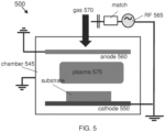
- PE-CVD method that may be used for forming DLC coatings in accordance with at least one embodiment is radio frequency plasma enhanced chemical vapor deposition (RF-PECVD).
- RF-PECVD radio frequency plasma enhanced chemical vapor deposition
- An example of an RF-PECVD reactor apparatus is shown generally at 500 in FIG. 5 .
- the reactor 500 typically includes a vacuum chamber 545 where a substrate is placed.
- a cathode 550 and an anode 560 are also disposed in the vacuum chamber 545, where deposition gas 570 is introduced.
- An RF power supply 565 generates RF potential that is applied to the deposition gas 570 to generate plasma 575. Electrons in the plasma ionize or dissociate reactant gases to generate radicals, which form the layer of deposition material on the sample. According to one embodiment, the deposition is performed at room temperature.
- the deposition gas 570 comprises a carbon containing gas, and in certain embodiments is a hydrocarbon.
- suitable hydrocarbons for use in forming the DLC coatings described herein include alkanes, such as methane, alkenes, such as ethylene, and alkynes, such as acetylene.
- Aromatic hydrocarbons, such as benzene, may also be used.
- the first DLC layer 112 is formed from a deposition gas 570 that consists of a hydrocarbon.
- the deposition gas 570 comprises a mixture of a carbon containing gas and an inert gas.
- the second DLC layer 114 is formed from a deposition gas 570 that comprises a mixture of a hydrocarbon and an inert gas.
- the deposition gas 570 used for forming the second DLC layer 114 includes at least 50% of an inert gas.
- Deposition parameters such as the hydrocarbon content in the gas mixture and the deposition time (for thickness) for each DLC layer included in the bilayer can be adjusted for a specific application.
- desired mechanical properties such as a desired hardness (e.g., based on military or industrial standards) for the DLC layer exposed to the external environment can be achieved by controlling the hydrocarbon content and/or thickness of the DLC layer.
- Multi-layer dielectric (MLD) film Multi-layer dielectric (MLD) film
- one or more multi-layer dielectric (MLD) films 120 are deposited on the substrate 105 for purposes of providing dual-band or multispectral spectral transmission.
- the transmission properties of the DLC coating 110 can be limited, and in some instances are limited to only a certain region of the IR spectrum.
- DLC films have high absorption in the visible and near-infrared regions.
- the thicker the DLC film the higher the absorption (but reducing thickness will reduce the durability).
- Combining the DLC coating 110 with one or more MLD films 120 allows for dual-band or multispectral functionality (e.g., a multispectral interference coating) of the optical element 100.
- Dual-band imaging typically includes using two distinct bands of wavelengths within the electromagnetic spectrum, whereas multispectral typically refers to two or more bands or ranges of wavelengths.
- the bands of wavelengths correspond to regions of the electromagnetic spectrum, such as the visible (VIS) region having wavelengths of approximately 400-750 nm, the near-infrared (NIR) region having wavelengths of approximately 750-1400 nm, the short-wavelength infrared (SWIR) region having wavelengths of approximately 1.4-3 microns, the mid-wavelength infrared (MWIR) region having wavelengths of approximately 3-8 microns, the long-wavelength infrared (LWIR) region having wavelengths of approximately 8-15 microns, and the far-infrared (FIR) region having wavelengths of approximately 15-1000 microns.
- VIS visible
- NIR near-infrared
- SWIR short-wavelength infrared
- MWIR mid-wavelength infrared
- LWIR long-wavelength infrared
- the MLD film 120 includes a plurality of layers, and the MLD film 120 is formed from two or more materials having different refractive indices. The two or more materials may be substantially transparent at one or more bands of wavelengths.
- the individual layers of the MLD film 120 may be formed from dielectric materials.
- dielectric material broadly refers to a material that is an electrical insulator or poor conductor of electric current; although according to some embodiments the MLD film 120 may include one or more layers that are typically characterized as semiconductors, such as germanium or silicon.
- the materials chosen for a particular MLD film 120 may be based on several factors, including the ability to transmit certain desired wavelengths of electromagnetic radiation, as discussed further below.
- the materials used in the MLD film 120 are transparent in the wavelength range of the particular application, such as a sensor.
- Non-limiting examples of materials that may be used in the MLD film 120 include oxides, sulfides, and selenides, such as titanium oxide, magnesium oxide, zinc oxide, silicon oxide, silicon dioxide (silica), aluminum oxide, indium sulfide, indium selenide, tin oxide, zinc sulfide, and zine selenide.
- materials that may be used in the MLD film 120 include fluorides, such as magnesium fluoride, yttrium fluoride, as well as silicon and germanium.
- the materials used in the MLD film 120 may be inorganic.
- two or more dielectric materials may be used in the MLD film 120.
- the materials used in the MLD film 120 may be deposited onto the substrate 105 using any one of a number of thin film vacuum deposition techniques, including chemical and physical vapor deposition methods.
- one or more layers of the MLD film 120 may be deposited using ion beam assisted deposition methods.
- the ion gun may be of the Kaufman type in which ions are formed in crossed electrical and magnetic fields.
- the MLD film 120 includes multiple layers of high, medium, and low refractive index dielectric materials.
- the thicknesses of the layers of material included in the MLD film 120 may also vary, as discussed further below.
- a particular configuration for the MLD film 120 may depend on several factors, including the wavelengths of interest, the thicknesses of the layers, and the variation of the index of refraction of the layers.
- the MLD film 120 includes alternating layers of high, medium, and low refractive index materials.
- the high, medium, and low refractive index comparison can be made at any one of a number of different reference wavelengths, and according to at least one embodiment, the reference wavelength is 550 nm.
- the high index material has an index of refraction that is greater than the medium index material, and the medium index material has an index of refraction that is greater than the low index material.
- a high index material may have an index of refraction of at least about 2.0 at 550 nm
- a medium index material may have an index of refraction between about 1.7 and about 2.0 at 550 nm
- a low index material may have an index of refraction of less than about 1.7 at 550 nm.
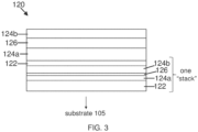
- the MLD film 120 includes multiple layers of material that are arranged in a repeating stack (which may also be referred to herein as a "period"). Each stack includes a high index material 122, a first medium index material 124a disposed over and contacting the high index material 122, a low index material 126 disposed over and contacting the first medium index material 124a, and a second medium index material 124b disposed over and contacting the low index material 126.
- the high index material 122 of the first stack is positioned either on or closest to the substrate 105.
- the first medium index material 124a and the second medium index material 124b are the same material, but they may each have different thickness values. In other embodiments, the first and second medium index materials 124a and 124b are different medium index materials.
- the example MLD film 120 shown in FIG. 3 includes two repeating "stacks" of high index, first medium index, low index, and second medium index materials, but it is to be appreciated that one or more than two “stacks” may be included in the MLD film 120.
- the "stack” may be "repeating" in that materials having high, medium, or low indices of refraction may be used in the same order in the stack, but each stack may have layers with different thicknesses than the corresponding layers in another stack.
- the example MLD film 120 shown in FIG. 3 includes a repeating stack of high, medium, low, and medium index materials, but other embodiments may include other types of repeating "stacks."
- the MLD film 120 may include a repeating stack of high index and low index materials such that the MLD film 120 comprises alternating layers of high and low index materials.
- a refractive index difference between a pair of layers adjacent to one another in the MLD film 120 is at least about 0.50.
- the refractive index difference is at least about 0.10.
- the refractive index difference is at least about 0.05.
- the MLD film 120 may include a repeating stack of high index and medium index materials, or medium index and low index materials. In some embodiments there is no repeating stack, but adjacent layers in the stack have different indices of refraction.
- each of the high index 122, medium index 124a and 124b, and low index 126 material layers has a different thickness.
- each layer in the MLD film 120 has a different thickness, but in other embodiments, the MLD film 120 includes two or more layers having the same thickness value.
- each layer of material included in the MLD film 120 may be characterized as being "thin,” meaning that the thickness does not exceed about two microns.
- the MLD film 120 includes one or more "stacks" of a high, low, and/or medium index material(s), and may also include one or more other separate layers that are disposed on (i.e., adjacent) and contact the "top” and/or “bottom” layer of the "stack.” These separate layer(s) have an index of refraction that is different than the index of refraction of the respective "top” and/or “bottom” layer of the MLD stack. For instance, using FIG. 3 as an example, an additional low index material 126 or high index material 122 may be positioned on top of the "top" medium index material 124b. The presence or absence of one or more of these types of separate layers depends on the configuration of the MLD film 120, including the configured transmission properties.
- the MLD film 120 may be configured to be substantially or completely transmissive to one or more bands of wavelengths of electromagnetic radiation. For instance, in some embodiments, the MLD film 120 is configured to transmit at least 90% of the waveband of interest (i.e., incoming radiation). According to one embodiment, the MLD film 120 is configured to be transmissive to at least two regions of the IR, e.g., LWIR and MWIR. According to another embodiment, the MLD film 120 is configured to be transmissive to both the VIS spectral range and at least one of the IR (e.g., NIR, SWIR, MWIR, LWIR, FIR) spectral regions.
- the IR e.g., NIR, SWIR, MWIR, LWIR, FIR
- an optical element 400 may include a first MLD film 120a disposed on one side or surface of the substrate 105, and a second MLD film 120b disposed on the opposite side of the substrate 105.
- the first MLD film 120a is configured to transmit light having a first band of wavelengths
- the second MLD film 120b is configured to transmit light having a second band of wavelengths
- a second multi-layer dielectric film disposed on the second surface of the substrate and constructed and arranged to transmit light in a second band of wavelengths, wherein the first and the second bands of wavelengths at least partially overlap.
- the first MLD film 120a may be configured to transmit light in a first region of the electromagnetic spectrum
- the second MLD film 120b may be configured to transmit light in a second region that at least partially overlaps with the first region.
- the first MLD film 120a may be configured as a long wave pass filter and the second MLD film 120b may be configured as a short wave pass filter.
- the first MLD film 120a may be configured as a short wave pass filter and the second MLD film 120b may be configured as a long wave pass filter. Since light is only transmitted for wavelengths where the first and second MLD films overlap, the combination of the first and second MLD films may function as a band pass filter for the optical element 400.
- the first and second MLD films 120a and 120b are configured to work in combination to transmit light in different regions of the IR spectrum, such as the MWIR and the LWIR.
- the first MLD film 120a may be configured to transmit light in a first band or bands of wavelengths
- the second MLD film 120b may be configured to transmit light in a second band or bands of wavelengths, such that MWIR and LWIR bands of wavelengths are transmitted (through 120b).
- the first MLD film 120a may be configured to transmit light in a first band or bands of wavelengths
- the second MLD film 120b may be configured to transmit light in a second band or bands of wavelengths, such that LWIR and MWIR band of wavelengths are transmitted.
- the first and second MLD films 120a and 120b are configured to transmit light in the VIS band of wavelengths and one of the IR regions of the electromagnetic spectrum, such as the NIR, FIR, LWIR, MWIR, or SWIR bands of wavelengths.
- the MLD film 120 may be configured to transmit a band of wavelengths within a spectral region, such as MWIR, VIS, NIR, etc. In some instances the band of wavelengths may be 20-100 nm wide, but it is to be appreciated that wider or narrower bands are within the scope of this disclosure. In reference to FIG. 4 , according to certain embodiments, the first MLD film 120a and the second MLD film 120b may be configured to transmit a band of wavelengths within two or more different spectral regions.
- a spectral region such as MWIR, VIS, NIR, etc.
- the band of wavelengths may be 20-100 nm wide, but it is to be appreciated that wider or narrower bands are within the scope of this disclosure.
- the first MLD film 120a and the second MLD film 120b may be configured to transmit a band of wavelengths within two or more different spectral regions.
- the first MLD film 120a is configured to transmit light having a first band of wavelengths
- the second MLD film 120b is configured to transmit light having a second band of wavelengths that is different than the first band of wavelengths.
- the first MLD film 120a may be configured to transmit light in one region of the electromagnetic spectrum
- the second MLD film 120b may be configured to transmit light in another, different region of the electromagnetic spectrum.
- the substrate 105 used in the optical elements 100 and 400 may be a substrate suitable for a particular application, and in some embodiments the substrate 105 is configured to transmit light in at least one of the band of wavelengths transmitted by the MLD film(s). In some embodiments, the substrate 105 is configured to transmit both the first and second bands of wavelengths of the dual-band (or multispectral) transmission of the MLD film(s). The choice of material for the substrate 105 may therefore depend on the transmission properties of the MLD film 120.
- the substrate 105 may be substrates known in the art, including UV fused silica, Pyrex ® , Zerodur ® , and other optical glasses, such as chalcogenide glass, as well as sapphire, silicon, germanium, etc.
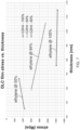
- RF power, total gas flow, and substrate temperature were all kept constant for each of the depositions.
- the process parameter that was varied included the percentage of inert gas (argon) in the total gas mixture (i.e., 0%, 16%, and 50%) (or 100% ethylene, 84% ethylene, and 50% ethylene), which affected the gas flow rate, the DC bias voltage, and the deposition rate.
- Table 1 below indicates the values for the deposition conditions.
- FIG. 7 plotting the stress versus thickness results for each of the three types of films: (1) ethylene @ 100%, (2) ethylene at 84%, and (3) ethylene at 50%.
- the Stoney's equation was used to calculate the stress values, and FIG. 7 indicates that compressive stress decreased as the argon content was increased.
- FIG. 7 also indicates that the stress increases as the thickness increases for the coatings having the highest ethylene content (i.e., 84% and 100%), whereas the stress decreases with thickness for the coating having the lowest ethylene concentration (50%).
- An optical element transmissive in the MWIR and LWIR spectral bands and coated with a bilayer DLC coating was constructed using an optical window substrate.
- the substrate 105 was formed from a one inch diameter, one millimeter thick germanium material.
- a first MLD film 120a was deposited on a first surface of the germanium substrate, and a second MLD film 120b was deposited on a second surface of the germanium substrate.
- An adhesion layer 130 consisting of 50 nm of germanium was deposited on the first MLD film 120a, and a DLC layer 110 was disposed on the adhesion layer 130.
- the first and second MLD films 120a and 120b were constructed from high, medium, and low index materials, with yttrium fluoride (YF 3 ) being the low index material, zinc sulfide (ZnS) being the medium index material, and germanium (Ge) being the high index material. These materials were input into an optical modeling software program (FILMSTAR TM , FTG Software Associates) as well as design criteria that included the desired transmittance bands (MWIR and LWIR). In this instance, each of the first and second MLD films 120a and 120b were configured to transmit both MWIR and LWIR.
- FILMSTAR TM optical modeling software program
- Each of the first and second MLD films 120a and 120b consisted of 11 repeating stacks of the high index, 1 st medium index (deposited on the high index), low index (deposited on the 1 st medium index), and 2 nd medium index (deposited on the low index) layers with thicknesses as shown in Tables 2 and 3 below.
- the 2 nd MLD film also had a layer of low index material (yttrium fluoride) deposited on the 11 th stack, as indicated in Table 3 below.
- the germanium was deposited with an electron beam gun.
- the yttrium fluoride and the zinc sulfide were deposited via thermal evaporation.
- a Kaufman type ion beam gun was used for ion-assisted deposition of yttrium fluoride and zinc sulfide layers, which was also used for cleaning the germanium substrate.
- the DLC layer 110 was 500 nm thick and comprised one bilayer, with each of the first layer and second layers of the bilayer having a thickness of 250 nm.
- the first and second bilayers were deposited at room temperature using an RF-PECVD coating chamber.
- the first layer of the bilayer was deposited on top of the 50 nm thick germanium adhesion layer 130 with a 50% argon/ethylene plasma mixture, and the second layer of the bilayer was deposited on top of the first layer with an ethylene plasma.
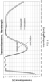
- FIGS. 8 and 9 Transmittance and reflectance tests were performed at normal incidence on the sample, with the results shown in FIGS. 8 and 9 , respectively.
- FIG. 8 shows the simulated and real transmittance through the window. The results indicated that the simulation and actual window transmittance values were in good agreement and that the window transmitted about 95% of the light for wavelengths of about 3.5 microns to about 5.0 microns and transmitted at least 90% of light for wavelengths of about 8.0 microns to about 10.5 microns.
- FIG. 9 shows the simulated and real reflectance values for light reflected from the interior side of the window (reflected from the 2 nd MLD film).
- the simulation and actual window results were in good agreement and indicated that the 2 nd MLD film reflected less than about 2% of light having wavelengths of about 3.5 microns to about 5.0 microns and about 8.0 microns to about 10.5 microns, which correlated with the transmittance results.
- a second window identical to the first window described above was constructed, except that the DLC coating of 500 nm thickness included two bilayer stacks, where each of the first and second layers in each of the bilayers was 125 nm in thickness.
- the DLC-coated side of this sample was subjected to a windscreen wiper test per RSRE Specification TS 1888, Section 5.4.3. The sample passed the test, which included exposing the window to 5000 revolutions of a wiper blade under a 40 gram load using a sand and water slurry mixture.
Landscapes
- Chemical & Material Sciences (AREA)
- Physics & Mathematics (AREA)
- Engineering & Computer Science (AREA)
- Organic Chemistry (AREA)
- Chemical Kinetics & Catalysis (AREA)
- Materials Engineering (AREA)
- Mechanical Engineering (AREA)
- Metallurgy (AREA)
- General Chemical & Material Sciences (AREA)
- General Physics & Mathematics (AREA)
- Optics & Photonics (AREA)
- Inorganic Chemistry (AREA)
- Plasma & Fusion (AREA)
- Crystallography & Structural Chemistry (AREA)
- Chemical Vapour Deposition (AREA)
- Laminated Bodies (AREA)
- Optical Filters (AREA)
Claims (13)
- Optisches Element (100), umfassend:ein Substrat (105), das eine erste Fläche und eine zweite Fläche aufweist, die gegenüberliegend der ersten Fläche angeordnet ist;eine erste mehrschichtige dielektrische Schicht (120), die auf der ersten Fläche des Substrats angeordnet ist und so aufgebaut und angeordnet ist, dass sie Licht in einem ersten Wellenlängenbereich überträgt;eine zweite mehrschichtige dielektrische Schicht (120), die auf der zweiten Fläche des Substrats (105) angeordnet ist und so aufgebaut und angeordnet ist, dass sie Licht in einem zweiten Wellenlängenband überträgt, wobei sich das erste und das zweite Wellenlängenband mindestens teilweise überlappen;eine zweischichtige diamantartige Kohlenstoffbeschichtung (diamond-like carbon, DLC) (110, 110a), die auf der ersten mehrschichtigen dielektrischen Schicht (120) angeordnet ist, wobei die zweischichtige DLC-Beschichtung (110, 110a) eine erste Schicht (112) und eine zweite Schicht (114) beinhaltet, wobei die erste Schicht (112) einen Elastizitätsmodul eines ersten Wertes aufweist und die zweite Schicht (114) auf der ersten Schicht (112) angeordnet ist und einen Elastizitätsmodul eines zweiten Wertes aufweist, der größer als der erste Wert ist; undeine Haftschicht (130), die zwischen der ersten mehrschichtigen dielektrischen Schicht (120) und der zweischichtigen DLC-Beschichtung (110) angeordnet ist; wobei mindestens eine der ersten mehrschichtigen dielektrischen Schicht und der zweiten mehrschichtigen dielektrischen Schicht einen oder mehrere Stapel aus Folgendem umfasst:einer dielektrischen Schicht (122) mit hohem Index;einer erste dielektrische Schicht (124a) mit mittlerem Index, die über und in Kontakt mit der Schicht (122) mit hohem Index angeordnet ist;einer dielektrischen Schicht (126) mit niedrigem Index, die über und in Kontakt mit der ersten Schicht (124a) mit mittlerem Index angeordnet ist; undeiner zweiten dielektrischen Schicht (124b) mit mittlerem Index, die über und in Kontakt mit der Schicht (126) mit niedrigem Index angeordnet ist, wobei die dielektrische Schicht (122) mit hohem Index einen Brechungsindex aufweist, der größer ist als der der ersten dielektrischen Schicht (124a) mit mittlerem Index, der zweiten dielektrischen Schicht (124b) mit mittlerem Index und der dielektrischen Schicht (126) mit niedrigem Index, und die Brechungsindizes der ersten und zweiten dielektrischen Schicht (124a, 124b) mit hohem Index größer sind als der Brechungsindex der dielektrischen Schicht (126) mit niedrigem Index; wobei das Material mit hohem Index entweder auf dem Substrat oder am nächsten zum Substrat positioniert ist; undwobei das erste und das zweite Wellenlängenband dazu konfiguriert sind, sichtbares (visible, VIS) Licht, das Wellenlängen von 0,4 bis 0,75 Mikrometer aufweist und mindestens eines von nahinfrarotem (near-infrared, NIR) Licht, das Wellenlängen von 0,75 bis 1,4 Mikrometer aufweist, kurzwelligem infrarotem (short-wavelength infrared, SWIR) Licht, das Wellenlängen von etwa 1,4 bis 3 Mikrometer aufweist, mittelwelliges Infrarotlicht (mid-wavelength infrared, MWIR), das Wellenlängen von etwa 3 bis 8 Mikrometer aufweist, langwelliges Infrarotlicht (long-wavelength infrared, LWIR), das Wellenlängen von etwa 8 bis 15 Mikrometer aufweist und fernes Infrarotlicht (far-infrared, FIR), das Wellenlängen von etwa 15 bis 1000 Mikrometer aufweist, zu übertragen.
- Optisches Element nach Anspruch 1, wobei die Haftschicht (130) aus einem von Silizium, Germanium und einem Oxid besteht.
- Optisches Element nach Anspruch 1, wobei die zweischichtige DLC-Beschichtung eine erste zweischichtige DLC-Beschichtung (116a) ist, das optische Element ferner eine zweite zweischichtige DLC-Beschichtung (116b) umfasst, die auf der ersten zweischichtigen DLC-Beschichtung (116a) angeordnet ist, und wobei das optische Element optional ferner mindestens eine zusätzliche zweischichtige DLC-Beschichtung umfasst, die auf der zweiten zweischichtigen DLC-Beschichtung (116b) angeordnet ist.
- Optisches Element nach Anspruch 1, wobei das erste und das zweite Wellenlängenband dazu konfiguriert sind, mittelwelliges Infrarotlicht (MWIR), das Wellenlängen von 3 bis 8 Mikrometern aufweist und langwelliges Infrarotlicht (LWIR), das Wellenlängen von 8 bis 15 Mikrometern aufweist, zu übertragen, optional wobei das Substrat dazu konfiguriert ist, MWIR- und LWIR-Licht zu übertragen.
- Optisches Element nach Anspruch 1, wobei die erste Schicht der DLC-Beschichtung (112) ein sp3/sp2-Verhältnis mit einem ersten Wert aufweist und die zweite Schicht der DLC-Beschichtung (114) ein sp3/sp2-Verhältnis mit einem zweiten Wert aufweist, der höher als der erste Wert ist.
- Optisches Element nach Anspruch 1, wobei die zweite Schicht der DLC-Beschichtung (114) aus sp3-gebundenem Kohlenstoff besteht.
- Optisches Element nach Anspruch 1, wobei die erste Schicht der DLC-Beschichtung (112) eine Mischung aus sp3- und sp2-gebundenem Kohlenstoff umfasst.
- Optisches Element nach Anspruch 1, wobei die zweischichtige DLC-Beschichtung (116) eine Dicke von mindestens 500 nm aufweist.
- Verfahren zum Bilden eines optischen Elements (100), umfassend:Bereitstellen eines Substrats (105), das eine erste Fläche und eine zweite Fläche aufweist, die gegenüberliegend der ersten Fläche angeordnet ist;Abscheiden einer ersten mehrschichtigen dielektrischen Schicht (120) auf der ersten Fläche des Substrats, sodass die erste mehrschichtige dielektrische Schicht (120) Licht, das eine erste Wellenlängenband aufweist, überträgt;Abscheiden einer zweiten mehrschichtigen dielektrischen Schicht (120) auf der zweiten Fläche des Substrats, sodass die zweite mehrschichtige dielektrische Schicht (120) Licht, das eine zweite Wellenlänge aufweist, überträgt, wobei sich die erste und die zweite Wellenlänge mindestens teilweise überlappen;Abscheiden einer Haftschicht (130) auf der ersten mehrschichtigen dielektrischen Schicht (120);Bilden einer ersten Schicht einer DLC-Beschichtung (112) auf der Haftschicht (130), die einen Elastizitätsmodul eines ersten Wertes aufweist; undBilden einer zweiten Schicht einer DLC-Beschichtung (114) auf der ersten Schicht der DLC-Beschichtung (112), die einen Elastizitätsmodul eines zweiten Wertes aufweist, der größer ist als der erste Wert; wobei mindestens eine der ersten mehrschichtigen dielektrischen Schicht (120) und der zweiten mehrschichtigen dielektrischen Schicht (120) einen oder mehrere Stapel aus Folgendem umfasst:einer dielektrischen Schicht (122) mit hohem Index;einer erste dielektrische Schicht (124a) mit mittlerem Index, die über und in Kontakt mit der Schicht (122) mit hohem Index angeordnet ist;einer dielektrischen Schicht (126) mit niedrigem Index, die über und in Kontakt mit der ersten Schicht (124a) mit mittlerem Index angeordnet ist; undeiner zweiten dielektrischen Schicht (124b) mit mittlerem Index, die über und in Kontakt mit der Schicht (126) mit niedrigem Index angeordnet ist, wobei die dielektrische Schicht (122) mit hohem Index einen Brechungsindex aufweist, der größer ist als der der ersten dielektrischen Schicht (124a) mit mittlerem Index, der zweiten dielektrischen Schicht (124b) mit mittlerem Index und der dielektrischen Schicht (126) mit niedrigem Index, und die Brechungsindizes der ersten und zweiten dielektrischen Schicht (124a, 124b) mit hohem Index größer sind als der Brechungsindex der dielektrischen Schicht (126) mit niedrigem Index; wobei das Material mit hohem Index entweder auf dem Substrat oder am nächsten zum Substrat positioniert ist; undwobei das erste und das zweite Wellenlängenband dazu konfiguriert sind, sichtbares (visible, VIS) Licht, das Wellenlängen von 0,4 bis 0,75 Mikrometer aufweist und mindestens eines von nahinfrarotem (near-infrared, NIR) Licht, das Wellenlängen von 0,75 bis 1,4 Mikrometer aufweist, kurzwelligem infrarotem (short-wavelength infrared, SWIR) Licht, das Wellenlängen von etwa 1,4 bis 3 Mikrometer aufweist, mittelwelliges Infrarotlicht (mid-wavelength infrared, MWIR), das Wellenlängen von etwa 3 bis 8 Mikrometer aufweist, langwelliges Infrarotlicht (long-wavelength infrared, LWIR), das Wellenlängen von etwa 8 bis 15 Mikrometer aufweist und fernes Infrarotlicht (far-infrared, FIR), das Wellenlängen von etwa 15 bis 1000 Mikrometer aufweist, zu übertragen.
- Verfahren nach Anspruch 9, wobei das Bilden der ersten und der zweiten Schicht der DLC-Beschichtung (112, 114) eine plasmaunterstützte chemische Gasphasenabscheidung (plasma enhanced chemical vapor deposition, PECVD) beinhaltet.
- Verfahren nach Anspruch 10, wobei die PECVD für die zweite Schicht der DLC-Beschichtung (114) ein Plasma beinhaltet, das aus einem Kohlenwasserstoff besteht.
- Verfahren nach Anspruch 10, wobei die PECVD für die erste Schicht der DLC-Beschichtung (112) ein Plasma beinhaltet, das aus einer Mischung aus einem Kohlenwasserstoff und einem Inertgas besteht, optional wobei die Mischung aus mindestens 50 % Inertgas besteht.
- Optisches Element nach Anspruch 12, wobei das Substrat (105) dazu konfiguriert ist, VIS und mindestens eines von NIR-, SWIR-, MWIR-, LWIR- und FIR-Licht zu übertragen.
Priority Applications (1)
| Application Number | Priority Date | Filing Date | Title |
|---|---|---|---|
| EP25185975.7A EP4606928A3 (de) | 2018-03-26 | 2019-03-25 | Multispektrale interferenzbeschichtung mit schicht aus diamantartigem kohlenstoff (dlc) |
Applications Claiming Priority (2)
| Application Number | Priority Date | Filing Date | Title |
|---|---|---|---|
| US15/935,675 US10705273B2 (en) | 2018-03-26 | 2018-03-26 | Multispectral interference coating with diamond-like carbon (DLC) film |
| PCT/US2019/023869 WO2019190980A1 (en) | 2018-03-26 | 2019-03-25 | Multispectral interference coating with diamond-like carbon (dlc) film |
Related Child Applications (1)
| Application Number | Title | Priority Date | Filing Date |
|---|---|---|---|
| EP25185975.7A Division EP4606928A3 (de) | 2018-03-26 | 2019-03-25 | Multispektrale interferenzbeschichtung mit schicht aus diamantartigem kohlenstoff (dlc) |
Publications (2)
| Publication Number | Publication Date |
|---|---|
| EP3776016A1 EP3776016A1 (de) | 2021-02-17 |
| EP3776016B1 true EP3776016B1 (de) | 2025-07-02 |
Family
ID=66223822
Family Applications (2)
| Application Number | Title | Priority Date | Filing Date |
|---|---|---|---|
| EP25185975.7A Pending EP4606928A3 (de) | 2018-03-26 | 2019-03-25 | Multispektrale interferenzbeschichtung mit schicht aus diamantartigem kohlenstoff (dlc) |
| EP19718506.9A Active EP3776016B1 (de) | 2018-03-26 | 2019-03-25 | Multispektrale interferenzbeschichtung mit schicht aus diamantartigem kohlenstoff (dlc) |
Family Applications Before (1)
| Application Number | Title | Priority Date | Filing Date |
|---|---|---|---|
| EP25185975.7A Pending EP4606928A3 (de) | 2018-03-26 | 2019-03-25 | Multispektrale interferenzbeschichtung mit schicht aus diamantartigem kohlenstoff (dlc) |
Country Status (4)
| Country | Link |
|---|---|
| US (1) | US10705273B2 (de) |
| EP (2) | EP4606928A3 (de) |
| CA (2) | CA3290491A1 (de) |
| WO (1) | WO2019190980A1 (de) |
Families Citing this family (3)
| Publication number | Priority date | Publication date | Assignee | Title |
|---|---|---|---|---|
| CN111323861B (zh) * | 2020-05-13 | 2021-12-03 | 翼捷安全设备(昆山)有限公司 | 乙炔气体探测用红外滤光片、制备方法及其应用 |
| US20220178026A1 (en) * | 2020-12-03 | 2022-06-09 | Applied Materials, Inc. | Carbon cvd deposition methods to mitigate stress induced defects |
| JP7638727B2 (ja) * | 2021-02-22 | 2025-03-04 | 東京エレクトロン株式会社 | 基板処理方法及び基板処理装置 |
Citations (3)
| Publication number | Priority date | Publication date | Assignee | Title |
|---|---|---|---|---|
| US20080286541A1 (en) * | 2006-03-17 | 2008-11-20 | Stefan Zeisler | Self-supporting multilayer films having a diamond-like carbon layer |
| US20090290219A1 (en) * | 2008-05-22 | 2009-11-26 | Etsuo Terayama | Reflection reducing film, optical member and optical system |
| JP2017128491A (ja) * | 2016-01-18 | 2017-07-27 | 住友電気工業株式会社 | 光学部品 |
Family Cites Families (16)
| Publication number | Priority date | Publication date | Assignee | Title |
|---|---|---|---|---|
| US4995684A (en) * | 1986-06-18 | 1991-02-26 | Raytheon Company | Impact resistant and tempered optical elements |
| GB9018608D0 (en) * | 1989-08-30 | 2013-11-13 | Texas Instruments Inc | Durable wideband anti-reflection coating for infrared windows |
| US5190807A (en) * | 1990-10-18 | 1993-03-02 | Diamonex, Incorporated | Abrasion wear resistant polymeric substrate product |
| US5470661A (en) * | 1993-01-07 | 1995-11-28 | International Business Machines Corporation | Diamond-like carbon films from a hydrocarbon helium plasma |
| US5482602A (en) | 1993-11-04 | 1996-01-09 | United Technologies Corporation | Broad-beam ion deposition coating methods for depositing diamond-like-carbon coatings on dynamic surfaces |
| EP0856592A1 (de) | 1997-02-04 | 1998-08-05 | N.V. Bekaert S.A. | Beschichtung enthaltende Filme aus diamantartigem Kohlenstoff und diamantartigem Nanokomposit |
| JP4256938B2 (ja) | 1997-02-04 | 2009-04-22 | ナムローゼ・フェンノートシャップ・ベーカート・ソシエテ・アノニム | ダイヤモンド状カーボン及びダイヤモンド状ナノコンポジット組成物の層を有するコーティング物 |
| US6277480B1 (en) * | 1999-05-03 | 2001-08-21 | Guardian Industries Corporation | Coated article including a DLC inclusive layer(s) and a layer(s) deposited using siloxane gas, and corresponding method |
| JP4958594B2 (ja) * | 2007-03-22 | 2012-06-20 | 富士フイルム株式会社 | 反射防止膜、光学素子および光学系 |
| CN101393276B (zh) * | 2007-09-21 | 2010-06-16 | 鸿富锦精密工业(深圳)有限公司 | 宽频带抗反射膜及具有该宽频带抗反射膜的光学元件 |
| CN101464528B (zh) | 2008-01-23 | 2011-01-12 | 四川大学 | 一种dlc红外抗反射保护膜及其制备方法 |
| DE102012010291A1 (de) * | 2012-05-18 | 2013-11-21 | Jenoptik Optical Systems Gmbh | Hybride DLC-Beschichtung für IR-Optiken |
| JP6202785B2 (ja) * | 2012-05-30 | 2017-09-27 | オリンパス株式会社 | 反射防止膜、光学系、光学機器、及び反射防止膜の成膜方法 |
| US9057887B1 (en) * | 2014-05-06 | 2015-06-16 | Blue Light Eye Protection, Inc. | Materials and methods for mitigating the harmful effects of blue light |
| US9335444B2 (en) * | 2014-05-12 | 2016-05-10 | Corning Incorporated | Durable and scratch-resistant anti-reflective articles |
| WO2018013462A2 (en) * | 2016-07-11 | 2018-01-18 | Corning Incorporated | Coatings of non-planar substrates and methods for the production thereof |
-
2018
- 2018-03-26 US US15/935,675 patent/US10705273B2/en active Active
-
2019
- 2019-03-25 EP EP25185975.7A patent/EP4606928A3/de active Pending
- 2019-03-25 CA CA3290491A patent/CA3290491A1/en active Pending
- 2019-03-25 WO PCT/US2019/023869 patent/WO2019190980A1/en not_active Ceased
- 2019-03-25 EP EP19718506.9A patent/EP3776016B1/de active Active
- 2019-03-25 CA CA3087719A patent/CA3087719C/en active Active
Patent Citations (4)
| Publication number | Priority date | Publication date | Assignee | Title |
|---|---|---|---|---|
| US20080286541A1 (en) * | 2006-03-17 | 2008-11-20 | Stefan Zeisler | Self-supporting multilayer films having a diamond-like carbon layer |
| US20090290219A1 (en) * | 2008-05-22 | 2009-11-26 | Etsuo Terayama | Reflection reducing film, optical member and optical system |
| JP2017128491A (ja) * | 2016-01-18 | 2017-07-27 | 住友電気工業株式会社 | 光学部品 |
| US20190023609A1 (en) * | 2016-01-18 | 2019-01-24 | Sumitomo Electric Industries, Ltd. | Optical component |
Also Published As
| Publication number | Publication date |
|---|---|
| EP3776016A1 (de) | 2021-02-17 |
| EP4606928A2 (de) | 2025-08-27 |
| EP4606928A3 (de) | 2025-11-19 |
| CA3290491A1 (en) | 2026-03-02 |
| WO2019190980A1 (en) | 2019-10-03 |
| US20190293850A1 (en) | 2019-09-26 |
| US10705273B2 (en) | 2020-07-07 |
| CA3087719C (en) | 2026-03-31 |
| CA3087719A1 (en) | 2019-10-03 |
Similar Documents
| Publication | Publication Date | Title |
|---|---|---|
| JP2024103644A (ja) | 改良された透過率を有する近赤外線光学干渉フィルタ | |
| CN105143930B (zh) | 用于高反射镜子的增强、耐用银涂层堆叠 | |
| AU2017286554B2 (en) | Protected item including a protective coating | |
| US20220221617A1 (en) | Curved surface films and methods of manufacturing the same | |
| EP3776016B1 (de) | Multispektrale interferenzbeschichtung mit schicht aus diamantartigem kohlenstoff (dlc) | |
| JP2020523642A (ja) | 高反射鏡のための銀コーティング積層体の反射帯域幅の拡大 | |
| US10131571B2 (en) | Methods of forming optical system components and optical coatings | |
| JP6713485B2 (ja) | 被覆された光学物体、および被覆された光学物体の製造方法 | |
| US7440204B2 (en) | ND filter of optical film laminate type with carbon film coating | |
| Lee et al. | Optical coatings on polymethyl methacrylate and polycarbonate | |
| US5688608A (en) | High refractive-index IR transparent window with hard, durable and antireflective coating | |
| US5770270A (en) | Protective and/or reflectivity enhancement of noble metal | |
| US6645608B2 (en) | Reflection reducing coating | |
| US20120263885A1 (en) | Method for the manufacture of a reflective layer system for back surface mirrors | |
| US20250155620A1 (en) | Optical coatings and optical elements | |
| CN117721428B (zh) | 一种可减弱蓝光的透明硬质涂层及制备工艺 | |
| US20250327166A1 (en) | Coating for a substrate; substrate; and article | |
| JPH01310302A (ja) | 分光フイルター | |
| JPH11231127A (ja) | 反射防止フイルム | |
| CN121918227A (zh) | 一种多功能光学薄膜及包含该薄膜的视力矫正镜片 | |
| JPH01222204A (ja) | 分光フイルター | |
| CN120028961A (zh) | 高性能宽光谱分色膜镀制方法 | |
| HK1237420B (zh) | 温度及腐蚀稳定的表面反射器 | |
| Oyama et al. | Absorptive anti-reflection coating for cathode ray tubes |
Legal Events
| Date | Code | Title | Description |
|---|---|---|---|
| STAA | Information on the status of an ep patent application or granted ep patent |
Free format text: STATUS: UNKNOWN |
|
| STAA | Information on the status of an ep patent application or granted ep patent |
Free format text: STATUS: THE INTERNATIONAL PUBLICATION HAS BEEN MADE |
|
| PUAI | Public reference made under article 153(3) epc to a published international application that has entered the european phase |
Free format text: ORIGINAL CODE: 0009012 |
|
| STAA | Information on the status of an ep patent application or granted ep patent |
Free format text: STATUS: REQUEST FOR EXAMINATION WAS MADE |
|
| 17P | Request for examination filed |
Effective date: 20201020 |
|
| AK | Designated contracting states |
Kind code of ref document: A1 Designated state(s): AL AT BE BG CH CY CZ DE DK EE ES FI FR GB GR HR HU IE IS IT LI LT LU LV MC MK MT NL NO PL PT RO RS SE SI SK SM TR |
|
| AX | Request for extension of the european patent |
Extension state: BA ME |
|
| RIN1 | Information on inventor provided before grant (corrected) |
Inventor name: CHIAO, SHU-CHUNG |
|
| DAV | Request for validation of the european patent (deleted) | ||
| DAX | Request for extension of the european patent (deleted) | ||
| STAA | Information on the status of an ep patent application or granted ep patent |
Free format text: STATUS: EXAMINATION IS IN PROGRESS |
|
| 17Q | First examination report despatched |
Effective date: 20230203 |
|
| GRAP | Despatch of communication of intention to grant a patent |
Free format text: ORIGINAL CODE: EPIDOSNIGR1 |
|
| STAA | Information on the status of an ep patent application or granted ep patent |
Free format text: STATUS: GRANT OF PATENT IS INTENDED |
|
| INTG | Intention to grant announced |
Effective date: 20241014 |
|
| RAP3 | Party data changed (applicant data changed or rights of an application transferred) |
Owner name: RAYTHEON COMPANY |
|
| GRAJ | Information related to disapproval of communication of intention to grant by the applicant or resumption of examination proceedings by the epo deleted |
Free format text: ORIGINAL CODE: EPIDOSDIGR1 |
|
| STAA | Information on the status of an ep patent application or granted ep patent |
Free format text: STATUS: EXAMINATION IS IN PROGRESS |
|
| GRAP | Despatch of communication of intention to grant a patent |
Free format text: ORIGINAL CODE: EPIDOSNIGR1 |
|
| STAA | Information on the status of an ep patent application or granted ep patent |
Free format text: STATUS: GRANT OF PATENT IS INTENDED |
|
| INTC | Intention to grant announced (deleted) | ||
| INTG | Intention to grant announced |
Effective date: 20250130 |
|
| GRAS | Grant fee paid |
Free format text: ORIGINAL CODE: EPIDOSNIGR3 |
|
| GRAA | (expected) grant |
Free format text: ORIGINAL CODE: 0009210 |
|
| STAA | Information on the status of an ep patent application or granted ep patent |
Free format text: STATUS: THE PATENT HAS BEEN GRANTED |
|
| AK | Designated contracting states |
Kind code of ref document: B1 Designated state(s): AL AT BE BG CH CY CZ DE DK EE ES FI FR GB GR HR HU IE IS IT LI LT LU LV MC MK MT NL NO PL PT RO RS SE SI SK SM TR |
|
| REG | Reference to a national code |
Ref country code: GB Ref legal event code: FG4D |
|
| REG | Reference to a national code |
Ref country code: CH Ref legal event code: EP |
|
| REG | Reference to a national code |
Ref country code: DE Ref legal event code: R096 Ref document number: 602019071901 Country of ref document: DE |
|
| REG | Reference to a national code |
Ref country code: SE Ref legal event code: TRGR |
|
| REG | Reference to a national code |
Ref country code: IE Ref legal event code: FG4D |
|
| REG | Reference to a national code |
Ref country code: NL Ref legal event code: MP Effective date: 20250702 |
|
| PG25 | Lapsed in a contracting state [announced via postgrant information from national office to epo] |
Ref country code: PT Free format text: LAPSE BECAUSE OF FAILURE TO SUBMIT A TRANSLATION OF THE DESCRIPTION OR TO PAY THE FEE WITHIN THE PRESCRIBED TIME-LIMIT Effective date: 20251103 |
|
| PG25 | Lapsed in a contracting state [announced via postgrant information from national office to epo] |
Ref country code: NL Free format text: LAPSE BECAUSE OF FAILURE TO SUBMIT A TRANSLATION OF THE DESCRIPTION OR TO PAY THE FEE WITHIN THE PRESCRIBED TIME-LIMIT Effective date: 20250702 |
|
| REG | Reference to a national code |
Ref country code: AT Ref legal event code: MK05 Ref document number: 1809851 Country of ref document: AT Kind code of ref document: T Effective date: 20250702 |
|
| PG25 | Lapsed in a contracting state [announced via postgrant information from national office to epo] |
Ref country code: IS Free format text: LAPSE BECAUSE OF FAILURE TO SUBMIT A TRANSLATION OF THE DESCRIPTION OR TO PAY THE FEE WITHIN THE PRESCRIBED TIME-LIMIT Effective date: 20251102 |
|
| PG25 | Lapsed in a contracting state [announced via postgrant information from national office to epo] |
Ref country code: NO Free format text: LAPSE BECAUSE OF FAILURE TO SUBMIT A TRANSLATION OF THE DESCRIPTION OR TO PAY THE FEE WITHIN THE PRESCRIBED TIME-LIMIT Effective date: 20251002 |
|
| REG | Reference to a national code |
Ref country code: LT Ref legal event code: MG9D |
|
| PG25 | Lapsed in a contracting state [announced via postgrant information from national office to epo] |
Ref country code: AT Free format text: LAPSE BECAUSE OF FAILURE TO SUBMIT A TRANSLATION OF THE DESCRIPTION OR TO PAY THE FEE WITHIN THE PRESCRIBED TIME-LIMIT Effective date: 20250702 |
|
| PG25 | Lapsed in a contracting state [announced via postgrant information from national office to epo] |
Ref country code: FI Free format text: LAPSE BECAUSE OF FAILURE TO SUBMIT A TRANSLATION OF THE DESCRIPTION OR TO PAY THE FEE WITHIN THE PRESCRIBED TIME-LIMIT Effective date: 20250702 |
|
| PG25 | Lapsed in a contracting state [announced via postgrant information from national office to epo] |
Ref country code: HR Free format text: LAPSE BECAUSE OF FAILURE TO SUBMIT A TRANSLATION OF THE DESCRIPTION OR TO PAY THE FEE WITHIN THE PRESCRIBED TIME-LIMIT Effective date: 20250702 |
|
| PG25 | Lapsed in a contracting state [announced via postgrant information from national office to epo] |
Ref country code: GR Free format text: LAPSE BECAUSE OF FAILURE TO SUBMIT A TRANSLATION OF THE DESCRIPTION OR TO PAY THE FEE WITHIN THE PRESCRIBED TIME-LIMIT Effective date: 20251003 |
|
| PG25 | Lapsed in a contracting state [announced via postgrant information from national office to epo] |
Ref country code: CZ Free format text: LAPSE BECAUSE OF FAILURE TO SUBMIT A TRANSLATION OF THE DESCRIPTION OR TO PAY THE FEE WITHIN THE PRESCRIBED TIME-LIMIT Effective date: 20250702 |
|
| PG25 | Lapsed in a contracting state [announced via postgrant information from national office to epo] |
Ref country code: LV Free format text: LAPSE BECAUSE OF FAILURE TO SUBMIT A TRANSLATION OF THE DESCRIPTION OR TO PAY THE FEE WITHIN THE PRESCRIBED TIME-LIMIT Effective date: 20250702 |
|
| PG25 | Lapsed in a contracting state [announced via postgrant information from national office to epo] |
Ref country code: BG Free format text: LAPSE BECAUSE OF FAILURE TO SUBMIT A TRANSLATION OF THE DESCRIPTION OR TO PAY THE FEE WITHIN THE PRESCRIBED TIME-LIMIT Effective date: 20250702 Ref country code: PL Free format text: LAPSE BECAUSE OF FAILURE TO SUBMIT A TRANSLATION OF THE DESCRIPTION OR TO PAY THE FEE WITHIN THE PRESCRIBED TIME-LIMIT Effective date: 20250702 |
|
| PG25 | Lapsed in a contracting state [announced via postgrant information from national office to epo] |
Ref country code: RS Free format text: LAPSE BECAUSE OF FAILURE TO SUBMIT A TRANSLATION OF THE DESCRIPTION OR TO PAY THE FEE WITHIN THE PRESCRIBED TIME-LIMIT Effective date: 20251002 |
|
| PG25 | Lapsed in a contracting state [announced via postgrant information from national office to epo] |
Ref country code: ES Free format text: LAPSE BECAUSE OF FAILURE TO SUBMIT A TRANSLATION OF THE DESCRIPTION OR TO PAY THE FEE WITHIN THE PRESCRIBED TIME-LIMIT Effective date: 20250702 |
|
| PG25 | Lapsed in a contracting state [announced via postgrant information from national office to epo] |
Ref country code: SM Free format text: LAPSE BECAUSE OF FAILURE TO SUBMIT A TRANSLATION OF THE DESCRIPTION OR TO PAY THE FEE WITHIN THE PRESCRIBED TIME-LIMIT Effective date: 20250702 |
|
| PGFP | Annual fee paid to national office [announced via postgrant information from national office to epo] |
Ref country code: SE Payment date: 20260219 Year of fee payment: 8 |
|
| PGFP | Annual fee paid to national office [announced via postgrant information from national office to epo] |
Ref country code: GB Payment date: 20260219 Year of fee payment: 8 |
|
| PG25 | Lapsed in a contracting state [announced via postgrant information from national office to epo] |
Ref country code: DK Free format text: LAPSE BECAUSE OF FAILURE TO SUBMIT A TRANSLATION OF THE DESCRIPTION OR TO PAY THE FEE WITHIN THE PRESCRIBED TIME-LIMIT Effective date: 20250702 |
|
| PGFP | Annual fee paid to national office [announced via postgrant information from national office to epo] |
Ref country code: DE Payment date: 20260219 Year of fee payment: 8 |
|
| PGFP | Annual fee paid to national office [announced via postgrant information from national office to epo] |
Ref country code: IT Payment date: 20260219 Year of fee payment: 8 |
|
| PGFP | Annual fee paid to national office [announced via postgrant information from national office to epo] |
Ref country code: FR Payment date: 20260219 Year of fee payment: 8 |
|
| PG25 | Lapsed in a contracting state [announced via postgrant information from national office to epo] |
Ref country code: SK Free format text: LAPSE BECAUSE OF FAILURE TO SUBMIT A TRANSLATION OF THE DESCRIPTION OR TO PAY THE FEE WITHIN THE PRESCRIBED TIME-LIMIT Effective date: 20250702 Ref country code: EE Free format text: LAPSE BECAUSE OF FAILURE TO SUBMIT A TRANSLATION OF THE DESCRIPTION OR TO PAY THE FEE WITHIN THE PRESCRIBED TIME-LIMIT Effective date: 20250702 |