EP3777049B1 - Circuit pour système de bus et procédé de fonctionnement d'un circuit - Google Patents
Circuit pour système de bus et procédé de fonctionnement d'un circuit Download PDFInfo
- Publication number
- EP3777049B1 EP3777049B1 EP19712988.5A EP19712988A EP3777049B1 EP 3777049 B1 EP3777049 B1 EP 3777049B1 EP 19712988 A EP19712988 A EP 19712988A EP 3777049 B1 EP3777049 B1 EP 3777049B1
- Authority
- EP
- European Patent Office
- Prior art keywords
- circuit
- resistance value
- bus
- resistance
- time window
- Prior art date
- Legal status (The legal status is an assumption and is not a legal conclusion. Google has not performed a legal analysis and makes no representation as to the accuracy of the status listed.)
- Active
Links
Images


Classifications
-
- G—PHYSICS
- G01—MEASURING; TESTING
- G01R—MEASURING ELECTRIC VARIABLES; MEASURING MAGNETIC VARIABLES
- G01R1/00—Details of instruments or arrangements of the types included in groups G01R5/00 - G01R13/00 and G01R31/00
- G01R1/20—Modifications of basic electric elements for use in electric measuring instruments; Structural combinations of such elements with such instruments
- G01R1/203—Resistors used for electric measuring, e.g. decade resistors standards, resistors for comparators, series resistors, shunts
-
- H—ELECTRICITY
- H04—ELECTRIC COMMUNICATION TECHNIQUE
- H04L—TRANSMISSION OF DIGITAL INFORMATION, e.g. TELEGRAPHIC COMMUNICATION
- H04L12/00—Data switching networks
- H04L12/28—Data switching networks characterised by path configuration, e.g. LAN [Local Area Networks] or WAN [Wide Area Networks]
- H04L12/40—Bus networks
- H04L12/40006—Architecture of a communication node
-
- H—ELECTRICITY
- H04—ELECTRIC COMMUNICATION TECHNIQUE
- H04L—TRANSMISSION OF DIGITAL INFORMATION, e.g. TELEGRAPHIC COMMUNICATION
- H04L25/00—Baseband systems
- H04L25/02—Details ; arrangements for supplying electrical power along data transmission lines
- H04L25/12—Compensating for variations in line impedance
-
- H—ELECTRICITY
- H04—ELECTRIC COMMUNICATION TECHNIQUE
- H04L—TRANSMISSION OF DIGITAL INFORMATION, e.g. TELEGRAPHIC COMMUNICATION
- H04L12/00—Data switching networks
- H04L12/28—Data switching networks characterised by path configuration, e.g. LAN [Local Area Networks] or WAN [Wide Area Networks]
- H04L12/40—Bus networks
- H04L2012/40208—Bus networks characterized by the use of a particular bus standard
- H04L2012/40215—Controller Area Network CAN
Definitions
- the invention relates to a circuit for a bus system and a method for operating a circuit for a bus system.
- bus oscillations are selectively masked out during data reception.
- a masking element is provided for masking oscillations of the bus signal for a predetermined masking time if a monitoring result shows that oscillations exceed a difference of the bus signal after a transition of the bus signal from a dominant to a recessive state by at least one predetermined threshold value.
- a bus system is known in which a terminating resistor is set depending on a measured impedance.
- the EP 1 202 451 A2 discloses an on-chip termination of transmission lines that enables the termination of transmission lines using on-chip resistors configured into networks whose resistances are referenced to the resistance of an external reference resistor.
- the WO 2015/185057 A1 reveals a Bus system with at least three control units for communication purposes, each control unit being assigned a bus terminating resistor with a predetermined resistance value for adapting a control unit resistor to a bus system resistor.
- the US 2010/177829 A1 discloses a receiver with an impedance control circuit. The impedance control circuit changes an input impedance based on a detected value.
- a circuit for a bus system comprises: a measuring circuit which is configured to measure a first resistance value between two bus-side connections of the circuit; a determination circuit which is configured to determine a second resistance value depending on the first resistance value; and a resistance circuit which is configured to set a resistor which can be switched between the two bus-side connections to the second resistance value.
- the resistor By setting the resistor to the second resistance value, it is advantageously achieved that the first resistance value which was measured at the bus-side connections - assuming that the resistor of the resistor circuit is activated with the second resistance value - is in a range in which communication via the bus system is maintained.
- a minimum value for the first resistance value of, for example, 50 ohms is not undercut.
- An advantageous embodiment is characterized in that the detection circuit is configured to increase the second resistance value when the first resistance value decreases. This increase in the second resistance value advantageously stabilizes the first resistance value, which improves the robustness of the communication via the bus system.
- the measuring circuit is configured to determine at least one time window depending on a message received via the two bus-side connections and depending on an a priori known position in relation to the received message, wherein the resistance circuit is configured to set the resistance connected between the two bus-side connections to the last determined second resistance value during the determined time window, and wherein the measuring circuit is configured to wait for a waiting period after the start of the time window and to measure the first resistance value between the two bus-side connections during a measuring period after the waiting period and before the end of the time window.
- the a priori known position in the message advantageously prevents negative effects on communication.
- An advantageous embodiment is characterized in that the length of the waiting time and/or the measuring time is one bit time or shorter. With a correctly configured bus system, it can be assumed that the signal propagation time is shorter than the bit time. The minimum specification of the bit time for the measuring time and the waiting time advantageously reduces negative effects on the measurement of the first resistance due to high signal propagation times in the bus system.
- An advantageous embodiment is characterized in that the resistance circuit is configured to determine the time window for switching on the resistance and to switch on the resistance during the time window with the last determined second resistance value, and wherein the measuring circuit is configured to determine the first resistance during the time window. Measurements are advantageously taken during the actual vibration damping, whereby the second resistance value is determined depending on the actual operation or the actual switching on for vibration damping. The second resistance value can thus be adapted more precisely to the desired damping effect.
- An advantageous embodiment is characterized in that the determination circuit is configured to determine the second resistance value depending on a comparison of the first resistance value with a target value for the first resistance value. It is advantageous to create a control loop which ensures that the bus system independently finds a value for the total resistance in order to carry out ringing suppression.
- An advantageous embodiment is characterized in that the determination circuit is configured to determine the second resistance value using a lookup table as a function of the first resistance value.
- the lookup table makes it easy to find the appropriate second resistance value.
- the circuit comprises: a configuration circuit which is configured to provide a number of subscriber stations of the bus system; and the determination circuit which is configured to determine the second resistance value using the lookup table as a function of the first resistance value and as a function of the number of subscriber stations provided.
- the second resistance value is adapted to the actual bus configuration. In particular, this prevents critical operating states which prevent a sharp drop in the first resistance value, in particular below the limit of 50 ohms.
- a further aspect of the description relates to a transceiver for a subscriber station of a bus system, wherein the transceiver comprises the circuit according to the first aspect.
- a further aspect of the description relates to a method for operating a circuit for a bus system, the method comprising: measuring a first resistance value between two bus-side terminals of the circuit; determining a second resistance value depending on the first resistance value; and setting a resistor switchable between the two bus-side terminals to the second resistance value, wherein at least one time window is determined depending on a message received via the two bus-side terminals and depending on an a priori known position in relation to the received message, wherein the resistance connected between the two bus-side terminals is set to the last determined second resistance value during the determined time window, and wherein a waiting period is waited for after a start of the time window in order to measure the first resistance value between the two bus-side terminals during a measuring period following the waiting period and before the end of the time window.
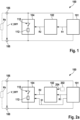
- Figure 1 shows a circuit 100 for a bus system.
- the circuit 100 comprises a measuring circuit 101, a detection circuit 102 and a resistance circuit 104, wherein the measuring circuit 101 and the resistance circuit 104 are arranged parallel to one another between two bus-side connections 106 and 108 of the circuit 100.
- the circuit 100 is connected to a first bus line CAN_H via the connection 106.
- the circuit 100 is connected to a second bus line CAN_L via the connection 108.
- a voltage V_DIFF drops between the two connections 106 and 108.
- the measuring circuit 101, the detection circuit 102 and the resistance circuit 104 are designed, for example, as an ASIC, FPGA or as a discrete circuit. Furthermore, the measuring circuit 101, the detection circuit 102 and the resistance circuit 104 comprise, for example, a processor that is equipped with software to execute the respective functions defined by software. Of course, mixed forms comprising a physical circuit and the processor on which the software is executed are also conceivable.
- the software is on a
- the circuit 100 is, for example, part of a transceiver for a subscriber station of a bus system. In another embodiment, the circuit 100 is implemented in addition to an existing transceiver.
- the resistance circuit 104 comprises a switch 110 and a resistor 112 arranged in series with it.
- the resistance circuit 104 can also be designed differently and, for example, comprise a MOS-FET.
- the resistor 112 is, for example, connected between the two bus-side connections 106, 108 when a state transition from a first state (for example dominant) of an absolute value of the voltage V_DIFF to a second state (for example recessive) occurs, for example, within a determined time window.
- the resistance circuit 104 serves to suppress or dampen oscillations of the voltage V_DIFF.
- the measuring circuit 101 determines a first resistance value R1 between the two bus-side connections 106 and 108.
- the first resistance value R1 is determined, for example, at regular intervals. For example, the determination can be carried out in every data frame or only once per minute.
- This first resistance value R1 reflects the total resistance connected between the two connections 106 and 108, which results, for example, from the parallel connection of a bus resistor Rb and the resistor 112.
- the determination circuit 102 determines a second resistance value R2 for the resistor 112 of the resistance circuit 104 depending on the supplied first resistance value R1. When the circuit starts, a predefined value is used for the second resistance value R2.
- the second resistance value R2 is supplied to the resistance circuit 104 in order to set the resistor 112 to the second resistance value R2.
- the resistance circuit 104 switches the resistance 112 between the two terminals 106 and 108 either on external request or independently, whereby the resistance 112 is set to the last determined resistance value R2.
- Figure 2a shows the circuit 100, wherein the measuring circuit 101 activates the resistance circuit 104 by means of a signal S1, so that the resistance connected between the two connections 106, 108 is also measured during the subsequent measurement.
- the measuring circuit 101 determines at least one time window depending on a message that is received via the bus or that is sent on the bus, and depending on a previously known position in relation to the message. Knowledge of the protocol is used for this purpose, in particular the presence of a message and its temporal position are determined depending on the voltage V_DIFF.
- the resistance circuit 100 is then operated using the signal S1 in such a way that the second resistance value R2 is set for the resistance connected between the connections 106, 108 during the determined time period.
- both the waiting time and the measurement time are one nominal bit time long because the nominal bit time consists of about 70% round trip time that must be waited for. In another example, the waiting time and the measurement time are shorter than the nominal bit time.
- a configuration circuit 202 provides a number 204 of subscriber stations of the bus system.
- the number 204 can either be preconfigured or the configuration circuit independently determines the number 204 of subscriber stations.
- the configuration circuit 202 exchanges messages with other bus subscribers.
- the determination circuit 102 can, for example, determine the second resistance value R2 to be smaller for an increased number 204 than for a reduced number 204.
- Figure 2b shows the circuit 100.
- a signal S2 is transmitted from the resistance circuit 104 to the measuring circuit 101.
- the resistance circuit 104 automatically determines the time window for switching on the resistance. The determination of the time window can be seen as a basic function for the operation of the resistance circuit.
- the signal S2 signals the measuring circuit 101 that the resistance is switched on; the time window is therefore transmitted to the measuring circuit 101. As long as the signal When S2 signals the connection of the resistor, the measuring circuit performs a measurement of the first resistor.
- Figure 3 shows the structure of a CAN message and the temporal arrangement of the measurement of the first resistance value.
- the message shown includes the following fields: Start of frame (SOF), Message Identifier (MID), Remote Transmission Request (RTR), Control field (CONTROL), Data Field (DATA), CRC field (CRC), Acknowledge field (ACK), End of Frame (EOF).
- SOF Start of frame
- MID Message Identifier
- RTR Remote Transmission Request
- CONTROL Control field
- DATA Data Field
- CRC field CRC field
- ACK Acknowledge field
- EEF End of Frame
- the resistance of the resistance circuit 104 is switched on in order to carry out the measurement of the first resistance value in the following fourth bit B4.
- the resistance of the resistance circuit is switched on and the first resistance value is measured within the intermission field, which is located between the end of frame EOF and the start of frame SOF.
- the third and fourth bits B3, B4 and the intermission field are particularly well suited to switching on the resistance of the resistance circuit
- Figure 4a shows the determination circuit 102 in a schematic section.
- a block 402 generates a setpoint R1s and feeds this to an addition point 404.
- the measured first resistance value R1 is subtracted from the setpoint R1s at the addition point 404 in order to determine a control difference d.
- a controller 406 determines the second resistance value R2 as a function of the control difference d, which in this case functions as a manipulated variable.
- the controller 406 can be, for example, a PID controller or a controller of another type.
- Figure 4b shows the determination circuit 102 in a schematic section.
- the configuration circuit 202 provides a block 410 with the number 204 of bus participants.
- the block 410 includes a lookup table which determines the second resistance value R2 depending on the number 204 and depending on the first resistance value R1.
- the lookup table is stored in a memory element.
- An even simpler variant is also conceivable in which the resistance R2 is determined using the block 410, which contains a lookup table, depending on the resistance R1.
- FIG. 5 shows an exemplary configured bus system comprising two subscriber stations 502, 504.
- Each of the subscriber stations 502, 504 comprises the respective circuit 100, which is connected with the first connection 106 to the first bus line CAN_H and with the second connection 108 to the second bus line CAN_L.
- the bus lines CAN_H and CAN_L are connected to one another at their ends via a respective terminating resistor Rb1 and Rb2.
- Rb1 and Rb2 By switching the resistor between the bus-side connections 106, 108 on and off, the respective circuits 100 of the subscriber stations 502 and 504 cause oscillations to be dampened and thus reduced when the state changes from dominant to recessive.
- the bus system 500 operates according to the embodiments in accordance with the CAN standard such as ISO11898.
- the circuit 100 and the operation of the circuit can, however, also be easily transferred to other bus systems. Other bus topologies are also conceivable.
Landscapes
- Engineering & Computer Science (AREA)
- Computer Networks & Wireless Communication (AREA)
- Signal Processing (AREA)
- Power Engineering (AREA)
- Physics & Mathematics (AREA)
- General Physics & Mathematics (AREA)
- Dc Digital Transmission (AREA)
- Small-Scale Networks (AREA)
Claims (9)
- Circuit (100) pour un système de bus, le circuit (100) comprenant :- un circuit de mesure (101) qui est configuré pour mesurer une première valeur de résistance entre deux bornes côté bus (106, 108) du circuit (100) ;- un circuit de détermination (102) qui est configuré pour déterminer une deuxième valeur de résistance en fonction de la première valeur de résistance ; et- un circuit de résistance (104) qui est configuré pour régler une résistance pouvant commuter entre les deux bornes côté bus (106, 108) sur la deuxième résistance, caractérisé en ce que le circuit de mesure (101) est configuré pour déterminer au moins une fenêtre temporelle en fonction d'un message reçu par l'intermédiaire des deux bornes côté bus (106, 108) et en fonction d'une position a priori connue par rapport au message reçu, dans lequel le circuit de résistance (104) est configuré pour régler la résistance connectée entre les deux bornes côté bus (106, 108) pendant la fenêtre temporelle déterminée sur la deuxième valeur de résistance déterminée en dernier, et dans lequel le circuit de mesure (101) est configuré pour attendre pendant une période d'attente après le début de la fenêtre temporelle et pour mesurer après la période d'attente et avant même la fin de la fenêtre temporelle la première valeur de résistance entre les deux bornes côté bus (106, 108) pendant une période de mesure.
- Circuit (100) selon la revendication 1, dans lequel le circuit de détermination (102) est configuré pour augmenter la deuxième valeur de résistance si la première valeur de résistance baisse.
- Circuit (100) selon la revendication 1, dans lequel la durée de la période d'attente et/ou de la période de mesure est un temps de bit ou moins.
- Circuit (100) selon l'une quelconque des revendications précédentes, dans lequel le circuit de résistance (104) est configuré pour déterminer une fenêtre temporelle pour mettre en circuit la résistance et pour mettre en circuit la résistance pendant la fenêtre temporelle avec la deuxième valeur de résistance déterminée en dernier, et dans lequel le circuit de mesure (101) est configuré pour déterminer la première résistance pendant la fenêtre temporelle.
- Circuit (100) selon l'une quelconque des revendications précédentes, dans lequel le circuit de détermination (102) est configuré pour déterminer la deuxième valeur de résistance en fonction d'une comparaison de la première valeur de résistance avec une valeur de consigne pour la première valeur de résistance.
- Circuit (100) selon l'une quelconque des revendications 1 à 4, dans lequel le circuit de détermination (102) est configuré pour déterminer la deuxième valeur de résistance au moyen d'une table de consultation en fonction de la première valeur de résistance.
- Circuit (100) selon la revendication 6, dans lequel le circuit (100) comprend :- un circuit de configuration (202) qui est configuré pour fournir un nombre donné (204) de stations d'abonné du système de bus ; et- le circuit de détermination (102) qui est configuré pour déterminer la deuxième valeur de résistance au moyen de la table de consultation en fonction de la première valeur de résistance et en fonction du nombre fourni (204) de stations d'abonné.
- Emetteur-récepteur pour une station d'abonné d'un système de bus, l'émetteur-récepteur comprenant le circuit (100) selon l'une quelconque des revendications 1 à 7.
- Procédé permettant de faire fonctionner un circuit (100) pour un système de bus, le procédé comprenant les étapes consistant à :- mesurer (101) une première valeur de résistance entre deux bornes côté bus (106, 108) du circuit (100) ;- déterminer (102) une deuxième valeur de résistance en fonction de la première valeur de résistance ; et- régler (104) une résistance pouvant être commutée entre les deux bornes côté bus sur la deuxième valeur de résistance, caractérisé en ce qu'au moins une fenêtre temporelle est déterminée en fonction d'un message reçu par l'intermédiaire des deux bornes côté bus (106, 108) et en fonction d'une position a priori connue par rapport au message reçu, dans lequel la résistance connectée entre les deux bornes côté bus (106, 108) pendant la fenêtre temporelle déterminée est réglée sur la deuxième valeur de résistance déterminée en dernier, et dans lequel on attend pendant une période d'attente après le début de la fenêtre temporelle afin de mesurer après la période d'attente et avant même la fin de la fenêtre temporelle la première valeur de résistance entre les deux bornes côté bus (106, 108) pendant une période de mesure.
Applications Claiming Priority (2)
| Application Number | Priority Date | Filing Date | Title |
|---|---|---|---|
| DE102018205217.4A DE102018205217A1 (de) | 2018-04-06 | 2018-04-06 | Schaltung für ein Bussystem und Verfahren zum Betreiben einer Schaltung |
| PCT/EP2019/057114 WO2019192851A1 (fr) | 2018-04-06 | 2019-03-21 | Circuit pour système de bus et procédé de fonctionnement d'un circuit |
Publications (2)
| Publication Number | Publication Date |
|---|---|
| EP3777049A1 EP3777049A1 (fr) | 2021-02-17 |
| EP3777049B1 true EP3777049B1 (fr) | 2024-09-04 |
Family
ID=65904429
Family Applications (1)
| Application Number | Title | Priority Date | Filing Date |
|---|---|---|---|
| EP19712988.5A Active EP3777049B1 (fr) | 2018-04-06 | 2019-03-21 | Circuit pour système de bus et procédé de fonctionnement d'un circuit |
Country Status (7)
| Country | Link |
|---|---|
| US (1) | US11585834B2 (fr) |
| EP (1) | EP3777049B1 (fr) |
| JP (1) | JP7066874B2 (fr) |
| KR (1) | KR102569849B1 (fr) |
| CN (1) | CN111971936B (fr) |
| DE (1) | DE102018205217A1 (fr) |
| WO (1) | WO2019192851A1 (fr) |
Families Citing this family (3)
| Publication number | Priority date | Publication date | Assignee | Title |
|---|---|---|---|---|
| DE102020206411A1 (de) * | 2020-05-22 | 2021-11-25 | Robert Bosch Gesellschaft mit beschränkter Haftung | Verfahren und Einrichtung zum Dämpfen von Schwingungen auf Busleitungen eines auf Differenzspannungssignalen basierenden Bussystems |
| US11394579B1 (en) * | 2021-06-21 | 2022-07-19 | Volvo Car Corporation | Smart controller area network termination |
| CN120035960A (zh) * | 2022-10-25 | 2025-05-23 | 松下知识产权经营株式会社 | 通信电路、装置、通信系统、通信电路的控制方法以及程序 |
Family Cites Families (24)
| Publication number | Priority date | Publication date | Assignee | Title |
|---|---|---|---|---|
| GB8419408D0 (en) * | 1984-07-30 | 1984-09-05 | Bicc Plc | Optical fibre splicing |
| JP2665517B2 (ja) * | 1989-09-29 | 1997-10-22 | 株式会社日立製作所 | 終端回路 |
| JPH06152610A (ja) * | 1992-11-06 | 1994-05-31 | Olympus Optical Co Ltd | データ伝送装置 |
| US6124727A (en) * | 1997-07-11 | 2000-09-26 | Adaptec, Inc. | Bias compensator for differential transmission line with voltage bias |
| US5977797A (en) * | 1997-12-30 | 1999-11-02 | Lsi Logic Corporation | Method and apparatus for transferring data on a voltage biased data line |
| US6605958B2 (en) | 2000-10-11 | 2003-08-12 | Vitesse Semiconductor Corporation | Precision on-chip transmission line termination |
| US6731132B2 (en) * | 2002-06-20 | 2004-05-04 | Texas Instruments Incorporated | Programmable line terminator |
| US7102381B2 (en) * | 2004-06-29 | 2006-09-05 | Intel Corporation | Adaptive termination for optimum signal detection |
| KR20090011807A (ko) * | 2007-07-27 | 2009-02-02 | 현대자동차주식회사 | 캔 통신라인의 종단저항 조절장치 |
| CN101521638A (zh) * | 2008-02-25 | 2009-09-02 | 陈�峰 | 高速接口终端负载的自动跟踪优化装置 |
| US8396164B2 (en) * | 2008-03-17 | 2013-03-12 | Denso Corporation | Receiving device including impedance control circuit and semiconductor device including impedance control circuit |
| JP4600523B2 (ja) * | 2008-06-09 | 2010-12-15 | ソニー株式会社 | 通信装置、通信システム、および通信方法 |
| US7999569B2 (en) | 2009-12-03 | 2011-08-16 | Nxp B.V. | Edge rate suppression for open drain buses |
| DE102010043484A1 (de) | 2010-11-05 | 2012-05-10 | Robert Bosch Gmbh | Vorrichtung und Verfahren zur seriellen Datenübertragung mit hoher Datenrate |
| AU2012381055B2 (en) * | 2012-05-21 | 2017-05-25 | Schneider Electric It Corporation | Systems and methods for biasing a bus |
| EP2804163B1 (fr) | 2013-05-17 | 2015-09-16 | Minimax GmbH & Co KG | Procédé et dispositif de détection des pannes dans des lignes de commande de systèmes de signalisation de danger et de systèmes de commande |
| DE102013214870B4 (de) | 2013-07-30 | 2026-05-21 | Robert Bosch Gmbh | Teilnehmerstation für ein Bussystem und Verfahren zur Verbesserung der Fehlerrobustheit einer Teilnehmerstation eines Bussystems |
| KR101823287B1 (ko) * | 2014-03-20 | 2018-01-29 | 닛본 덴끼 가부시끼가이샤 | 종단 장치, 종단 제어 방법, 및 종단 제어 프로그램이 기억된 기억매체 |
| DE102014210698A1 (de) | 2014-06-05 | 2015-12-17 | Schaeffler Technologies AG & Co. KG | Terminierung eines Bussystems, vorzugsweise für einen Einsatz in einem Doppelkupplungsgetriebe |
| DE102015222334A1 (de) | 2015-11-12 | 2017-05-18 | Robert Bosch Gmbh | Einrichtung und Verfahren zum selektiven Ausblenden von Busschwingungen beim Datenempfang über ein Bussystem |
| CN106302063A (zh) * | 2016-08-12 | 2017-01-04 | 深圳市沃特玛电池有限公司 | Can通信线电路系统及其终端电阻接入控制方法 |
| DE102018104732B3 (de) * | 2018-03-01 | 2019-02-21 | Infineon Technologies Ag | Bus-treiberschaltung |
| US10615996B2 (en) * | 2018-03-14 | 2020-04-07 | Nxp B.V. | Apparatuses and methods for switching communication modes of a transceiver circuit |
| EP3809638B1 (fr) * | 2019-10-17 | 2023-05-17 | Volvo Car Corporation | Détection de manipulation de données sur un bus can |
-
2018
- 2018-04-06 DE DE102018205217.4A patent/DE102018205217A1/de active Pending
-
2019
- 2019-03-21 US US16/981,163 patent/US11585834B2/en active Active
- 2019-03-21 KR KR1020207031977A patent/KR102569849B1/ko active Active
- 2019-03-21 JP JP2020554522A patent/JP7066874B2/ja active Active
- 2019-03-21 WO PCT/EP2019/057114 patent/WO2019192851A1/fr not_active Ceased
- 2019-03-21 CN CN201980024221.3A patent/CN111971936B/zh active Active
- 2019-03-21 EP EP19712988.5A patent/EP3777049B1/fr active Active
Also Published As
| Publication number | Publication date |
|---|---|
| CN111971936A (zh) | 2020-11-20 |
| US11585834B2 (en) | 2023-02-21 |
| JP2021520735A (ja) | 2021-08-19 |
| CN111971936B (zh) | 2022-05-17 |
| KR20200138819A (ko) | 2020-12-10 |
| JP7066874B2 (ja) | 2022-05-13 |
| KR102569849B1 (ko) | 2023-08-24 |
| WO2019192851A1 (fr) | 2019-10-10 |
| US20210063444A1 (en) | 2021-03-04 |
| DE102018205217A1 (de) | 2019-10-10 |
| EP3777049A1 (fr) | 2021-02-17 |
Similar Documents
| Publication | Publication Date | Title |
|---|---|---|
| EP3114800B1 (fr) | Station d'abonné pour un système de bus et procédé d'amélioration de la qualité d'émission dans un système de bus | |
| EP3114801B1 (fr) | Station d'abonné pour un système de bus et procédé de réduction d'émissions liées à une ligne dans un système de bus | |
| EP3066792B1 (fr) | Station de participant à un système de bus et procédé pour améliorer la qualité de réception dans un système de bus | |
| DE102013218075A1 (de) | Vorrichtung und Messverfahren zur Ermittlung der internen Verzögerungszeit einer CAN-Busanschlusseinheit | |
| WO2019030080A1 (fr) | Dispositif d'émission / réception pour un système de bus et procédé de réduction d'une disposition aux oscillations lors de la transition entre différents états binaires | |
| EP3777049A1 (fr) | Circuit pour système de bus et procédé de fonctionnement d'un circuit | |
| DE102014222661B4 (de) | Anordnung und Verfahren zur Optimierung der Übertragung von digitalen Daten in Zweidraht-Kommunikations-Netzwerken | |
| EP3756311B1 (fr) | Dispositif et procédé destinés à un moyen émetteur-récepteur d'un système de bus | |
| DE102017213834A1 (de) | Sende-/Empfangseinrichtung für ein Bussystem und Verfahren zur Reduzierung einer Schwingneigung beim Übergang zwischen unterschiedlichen Bitzuständen | |
| DE102020128430B4 (de) | Feldbussystem mit umschaltbarer slew-rate | |
| DE102014210505A1 (de) | Übertragungseinheit mit Prüffunktion | |
| DE602005000282T2 (de) | Verfahren und Vorrichtung zur automatischen Erkennung der Bitrate von CAN-Bus-Netzwerk | |
| WO2019029974A1 (fr) | Dispositif d'émission/réception pour systeme de bus et procédé de réduction de la tendance à osciller entre differents états binaires | |
| DE102019116657B4 (de) | System und Verfahren zur kombinierten Energieübertragung und Datenübertragung in einem Automatisierungssystem | |
| EP3665874B1 (fr) | Dispositif d'émission/réception pour systeme de bus et procédé de réduction de la tendance à osciller lors de la transition entre différents état binaires | |
| DE102010001842B4 (de) | Kommunikationssystem mit Signalreflexionsverhinderungsfunktion und im System vorhandener Knoten | |
| DE102019220022A1 (de) | Sende-/Empfangseinrichtung für ein Bussystem und Verfahren zur Reduzierung von Schwingungen einer Busdifferenzspannung bei eingekoppelten Störungen | |
| DE102018206522A1 (de) | Vorrichtung und Verfahren zum Auswerten eines über ein Bussystem empfangbaren Empfangssignals | |
| EP1684457B1 (fr) | Dispositif d'alimentation de tension pour un coupleur de bus et procédé d'operation correspondant | |
| EP1193890B1 (fr) | Méthode et appareil pour diagnostiquer une ligne de transmission d'un système de bus | |
| DE102018206926A1 (de) | Schaltung für ein Bussystem und Verfahren zum Betreiben einer Schaltung | |
| WO2019211825A1 (fr) | Circuit conçu pour un système de bus et procédé pour faire fonctionner un circuit | |
| DE102017223417A1 (de) | Verfahren zum Selbsttest, Datenbusanordnung und Verwendung | |
| DE102017216484A1 (de) | Verfahren zur Signalübertragung, Datenbusanordnung und korrespondierende Verwendung | |
| DE102020205671A1 (de) | Konfiguration eines Bussystems |
Legal Events
| Date | Code | Title | Description |
|---|---|---|---|
| STAA | Information on the status of an ep patent application or granted ep patent |
Free format text: STATUS: UNKNOWN |
|
| STAA | Information on the status of an ep patent application or granted ep patent |
Free format text: STATUS: THE INTERNATIONAL PUBLICATION HAS BEEN MADE |
|
| PUAI | Public reference made under article 153(3) epc to a published international application that has entered the european phase |
Free format text: ORIGINAL CODE: 0009012 |
|
| STAA | Information on the status of an ep patent application or granted ep patent |
Free format text: STATUS: REQUEST FOR EXAMINATION WAS MADE |
|
| 17P | Request for examination filed |
Effective date: 20201106 |
|
| AK | Designated contracting states |
Kind code of ref document: A1 Designated state(s): AL AT BE BG CH CY CZ DE DK EE ES FI FR GB GR HR HU IE IS IT LI LT LU LV MC MK MT NL NO PL PT RO RS SE SI SK SM TR |
|
| AX | Request for extension of the european patent |
Extension state: BA ME |
|
| DAV | Request for validation of the european patent (deleted) | ||
| DAX | Request for extension of the european patent (deleted) | ||
| STAA | Information on the status of an ep patent application or granted ep patent |
Free format text: STATUS: EXAMINATION IS IN PROGRESS |
|
| 17Q | First examination report despatched |
Effective date: 20230102 |
|
| GRAP | Despatch of communication of intention to grant a patent |
Free format text: ORIGINAL CODE: EPIDOSNIGR1 |
|
| STAA | Information on the status of an ep patent application or granted ep patent |
Free format text: STATUS: GRANT OF PATENT IS INTENDED |
|
| INTG | Intention to grant announced |
Effective date: 20240619 |
|
| GRAS | Grant fee paid |
Free format text: ORIGINAL CODE: EPIDOSNIGR3 |
|
| GRAA | (expected) grant |
Free format text: ORIGINAL CODE: 0009210 |
|
| STAA | Information on the status of an ep patent application or granted ep patent |
Free format text: STATUS: THE PATENT HAS BEEN GRANTED |
|
| AK | Designated contracting states |
Kind code of ref document: B1 Designated state(s): AL AT BE BG CH CY CZ DE DK EE ES FI FR GB GR HR HU IE IS IT LI LT LU LV MC MK MT NL NO PL PT RO RS SE SI SK SM TR |
|
| REG | Reference to a national code |
Ref country code: GB Ref legal event code: FG4D Free format text: NOT ENGLISH |
|
| REG | Reference to a national code |
Ref country code: CH Ref legal event code: EP |
|
| REG | Reference to a national code |
Ref country code: IE Ref legal event code: FG4D Free format text: LANGUAGE OF EP DOCUMENT: GERMAN |
|
| REG | Reference to a national code |
Ref country code: DE Ref legal event code: R096 Ref document number: 502019012042 Country of ref document: DE |
|
| REG | Reference to a national code |
Ref country code: LT Ref legal event code: MG9D |
|
| REG | Reference to a national code |
Ref country code: NL Ref legal event code: MP Effective date: 20240904 |
|
| PG25 | Lapsed in a contracting state [announced via postgrant information from national office to epo] |
Ref country code: NO Free format text: LAPSE BECAUSE OF FAILURE TO SUBMIT A TRANSLATION OF THE DESCRIPTION OR TO PAY THE FEE WITHIN THE PRESCRIBED TIME-LIMIT Effective date: 20241204 |
|
| PG25 | Lapsed in a contracting state [announced via postgrant information from national office to epo] |
Ref country code: GR Free format text: LAPSE BECAUSE OF FAILURE TO SUBMIT A TRANSLATION OF THE DESCRIPTION OR TO PAY THE FEE WITHIN THE PRESCRIBED TIME-LIMIT Effective date: 20241205 Ref country code: PL Free format text: LAPSE BECAUSE OF FAILURE TO SUBMIT A TRANSLATION OF THE DESCRIPTION OR TO PAY THE FEE WITHIN THE PRESCRIBED TIME-LIMIT Effective date: 20240904 Ref country code: FI Free format text: LAPSE BECAUSE OF FAILURE TO SUBMIT A TRANSLATION OF THE DESCRIPTION OR TO PAY THE FEE WITHIN THE PRESCRIBED TIME-LIMIT Effective date: 20240904 |
|
| PG25 | Lapsed in a contracting state [announced via postgrant information from national office to epo] |
Ref country code: BG Free format text: LAPSE BECAUSE OF FAILURE TO SUBMIT A TRANSLATION OF THE DESCRIPTION OR TO PAY THE FEE WITHIN THE PRESCRIBED TIME-LIMIT Effective date: 20240904 |
|
| PG25 | Lapsed in a contracting state [announced via postgrant information from national office to epo] |
Ref country code: LV Free format text: LAPSE BECAUSE OF FAILURE TO SUBMIT A TRANSLATION OF THE DESCRIPTION OR TO PAY THE FEE WITHIN THE PRESCRIBED TIME-LIMIT Effective date: 20240904 |
|
| PG25 | Lapsed in a contracting state [announced via postgrant information from national office to epo] |
Ref country code: HR Free format text: LAPSE BECAUSE OF FAILURE TO SUBMIT A TRANSLATION OF THE DESCRIPTION OR TO PAY THE FEE WITHIN THE PRESCRIBED TIME-LIMIT Effective date: 20240904 |
|
| PG25 | Lapsed in a contracting state [announced via postgrant information from national office to epo] |
Ref country code: ES Free format text: LAPSE BECAUSE OF FAILURE TO SUBMIT A TRANSLATION OF THE DESCRIPTION OR TO PAY THE FEE WITHIN THE PRESCRIBED TIME-LIMIT Effective date: 20240904 Ref country code: RS Free format text: LAPSE BECAUSE OF FAILURE TO SUBMIT A TRANSLATION OF THE DESCRIPTION OR TO PAY THE FEE WITHIN THE PRESCRIBED TIME-LIMIT Effective date: 20241204 |
|
| PG25 | Lapsed in a contracting state [announced via postgrant information from national office to epo] |
Ref country code: RS Free format text: LAPSE BECAUSE OF FAILURE TO SUBMIT A TRANSLATION OF THE DESCRIPTION OR TO PAY THE FEE WITHIN THE PRESCRIBED TIME-LIMIT Effective date: 20241204 Ref country code: PL Free format text: LAPSE BECAUSE OF FAILURE TO SUBMIT A TRANSLATION OF THE DESCRIPTION OR TO PAY THE FEE WITHIN THE PRESCRIBED TIME-LIMIT Effective date: 20240904 Ref country code: NO Free format text: LAPSE BECAUSE OF FAILURE TO SUBMIT A TRANSLATION OF THE DESCRIPTION OR TO PAY THE FEE WITHIN THE PRESCRIBED TIME-LIMIT Effective date: 20241204 Ref country code: LV Free format text: LAPSE BECAUSE OF FAILURE TO SUBMIT A TRANSLATION OF THE DESCRIPTION OR TO PAY THE FEE WITHIN THE PRESCRIBED TIME-LIMIT Effective date: 20240904 Ref country code: HR Free format text: LAPSE BECAUSE OF FAILURE TO SUBMIT A TRANSLATION OF THE DESCRIPTION OR TO PAY THE FEE WITHIN THE PRESCRIBED TIME-LIMIT Effective date: 20240904 Ref country code: GR Free format text: LAPSE BECAUSE OF FAILURE TO SUBMIT A TRANSLATION OF THE DESCRIPTION OR TO PAY THE FEE WITHIN THE PRESCRIBED TIME-LIMIT Effective date: 20241205 Ref country code: FI Free format text: LAPSE BECAUSE OF FAILURE TO SUBMIT A TRANSLATION OF THE DESCRIPTION OR TO PAY THE FEE WITHIN THE PRESCRIBED TIME-LIMIT Effective date: 20240904 Ref country code: ES Free format text: LAPSE BECAUSE OF FAILURE TO SUBMIT A TRANSLATION OF THE DESCRIPTION OR TO PAY THE FEE WITHIN THE PRESCRIBED TIME-LIMIT Effective date: 20240904 Ref country code: BG Free format text: LAPSE BECAUSE OF FAILURE TO SUBMIT A TRANSLATION OF THE DESCRIPTION OR TO PAY THE FEE WITHIN THE PRESCRIBED TIME-LIMIT Effective date: 20240904 |
|
| PG25 | Lapsed in a contracting state [announced via postgrant information from national office to epo] |
Ref country code: NL Free format text: LAPSE BECAUSE OF FAILURE TO SUBMIT A TRANSLATION OF THE DESCRIPTION OR TO PAY THE FEE WITHIN THE PRESCRIBED TIME-LIMIT Effective date: 20240904 |
|
| PG25 | Lapsed in a contracting state [announced via postgrant information from national office to epo] |
Ref country code: PT Free format text: LAPSE BECAUSE OF FAILURE TO SUBMIT A TRANSLATION OF THE DESCRIPTION OR TO PAY THE FEE WITHIN THE PRESCRIBED TIME-LIMIT Effective date: 20250106 Ref country code: IS Free format text: LAPSE BECAUSE OF FAILURE TO SUBMIT A TRANSLATION OF THE DESCRIPTION OR TO PAY THE FEE WITHIN THE PRESCRIBED TIME-LIMIT Effective date: 20250104 |
|
| PG25 | Lapsed in a contracting state [announced via postgrant information from national office to epo] |
Ref country code: SM Free format text: LAPSE BECAUSE OF FAILURE TO SUBMIT A TRANSLATION OF THE DESCRIPTION OR TO PAY THE FEE WITHIN THE PRESCRIBED TIME-LIMIT Effective date: 20240904 Ref country code: RO Free format text: LAPSE BECAUSE OF FAILURE TO SUBMIT A TRANSLATION OF THE DESCRIPTION OR TO PAY THE FEE WITHIN THE PRESCRIBED TIME-LIMIT Effective date: 20240904 |
|
| PG25 | Lapsed in a contracting state [announced via postgrant information from national office to epo] |
Ref country code: EE Free format text: LAPSE BECAUSE OF FAILURE TO SUBMIT A TRANSLATION OF THE DESCRIPTION OR TO PAY THE FEE WITHIN THE PRESCRIBED TIME-LIMIT Effective date: 20240904 |
|
| PG25 | Lapsed in a contracting state [announced via postgrant information from national office to epo] |
Ref country code: CZ Free format text: LAPSE BECAUSE OF FAILURE TO SUBMIT A TRANSLATION OF THE DESCRIPTION OR TO PAY THE FEE WITHIN THE PRESCRIBED TIME-LIMIT Effective date: 20240904 |
|
| PGFP | Annual fee paid to national office [announced via postgrant information from national office to epo] |
Ref country code: FR Payment date: 20250324 Year of fee payment: 7 |
|
| PG25 | Lapsed in a contracting state [announced via postgrant information from national office to epo] |
Ref country code: SK Free format text: LAPSE BECAUSE OF FAILURE TO SUBMIT A TRANSLATION OF THE DESCRIPTION OR TO PAY THE FEE WITHIN THE PRESCRIBED TIME-LIMIT Effective date: 20240904 |
|
| REG | Reference to a national code |
Ref country code: DE Ref legal event code: R097 Ref document number: 502019012042 Country of ref document: DE |
|
| PGFP | Annual fee paid to national office [announced via postgrant information from national office to epo] |
Ref country code: DE Payment date: 20250522 Year of fee payment: 7 |
|
| PG25 | Lapsed in a contracting state [announced via postgrant information from national office to epo] |
Ref country code: DK Free format text: LAPSE BECAUSE OF FAILURE TO SUBMIT A TRANSLATION OF THE DESCRIPTION OR TO PAY THE FEE WITHIN THE PRESCRIBED TIME-LIMIT Effective date: 20240904 |
|
| PLBE | No opposition filed within time limit |
Free format text: ORIGINAL CODE: 0009261 |
|
| STAA | Information on the status of an ep patent application or granted ep patent |
Free format text: STATUS: NO OPPOSITION FILED WITHIN TIME LIMIT |
|
| PGFP | Annual fee paid to national office [announced via postgrant information from national office to epo] |
Ref country code: IT Payment date: 20250331 Year of fee payment: 7 |
|
| 26N | No opposition filed |
Effective date: 20250605 |
|
| PG25 | Lapsed in a contracting state [announced via postgrant information from national office to epo] |
Ref country code: SE Free format text: LAPSE BECAUSE OF FAILURE TO SUBMIT A TRANSLATION OF THE DESCRIPTION OR TO PAY THE FEE WITHIN THE PRESCRIBED TIME-LIMIT Effective date: 20240904 |
|
| PG25 | Lapsed in a contracting state [announced via postgrant information from national office to epo] |
Ref country code: MC Free format text: LAPSE BECAUSE OF FAILURE TO SUBMIT A TRANSLATION OF THE DESCRIPTION OR TO PAY THE FEE WITHIN THE PRESCRIBED TIME-LIMIT Effective date: 20240904 |
|
| REG | Reference to a national code |
Ref country code: CH Ref legal event code: H13 Free format text: ST27 STATUS EVENT CODE: U-0-0-H10-H13 (AS PROVIDED BY THE NATIONAL OFFICE) Effective date: 20251024 |
|
| PG25 | Lapsed in a contracting state [announced via postgrant information from national office to epo] |
Ref country code: LU Free format text: LAPSE BECAUSE OF NON-PAYMENT OF DUE FEES Effective date: 20250321 |
|
| GBPC | Gb: european patent ceased through non-payment of renewal fee |
Effective date: 20250321 |
|
| REG | Reference to a national code |
Ref country code: BE Ref legal event code: MM Effective date: 20250331 |
|
| PG25 | Lapsed in a contracting state [announced via postgrant information from national office to epo] |
Ref country code: GB Free format text: LAPSE BECAUSE OF NON-PAYMENT OF DUE FEES Effective date: 20250321 |
|
| PG25 | Lapsed in a contracting state [announced via postgrant information from national office to epo] |
Ref country code: BE Free format text: LAPSE BECAUSE OF NON-PAYMENT OF DUE FEES Effective date: 20250331 |
|
| PG25 | Lapsed in a contracting state [announced via postgrant information from national office to epo] |
Ref country code: CH Free format text: LAPSE BECAUSE OF NON-PAYMENT OF DUE FEES Effective date: 20250331 |
|
| PG25 | Lapsed in a contracting state [announced via postgrant information from national office to epo] |
Ref country code: IE Free format text: LAPSE BECAUSE OF NON-PAYMENT OF DUE FEES Effective date: 20250321 |