EP3779574A1 - Optisches element - Google Patents
Optisches element Download PDFInfo
- Publication number
- EP3779574A1 EP3779574A1 EP19776059.8A EP19776059A EP3779574A1 EP 3779574 A1 EP3779574 A1 EP 3779574A1 EP 19776059 A EP19776059 A EP 19776059A EP 3779574 A1 EP3779574 A1 EP 3779574A1
- Authority
- EP
- European Patent Office
- Prior art keywords
- substrate
- electrode
- contact
- optical element
- contact metal
- Prior art date
- Legal status (The legal status is an assumption and is not a legal conclusion. Google has not performed a legal analysis and makes no representation as to the accuracy of the status listed.)
- Granted
Links
Images




Classifications
-
- G—PHYSICS
- G02—OPTICS
- G02F—OPTICAL DEVICES OR ARRANGEMENTS FOR THE CONTROL OF LIGHT BY MODIFICATION OF THE OPTICAL PROPERTIES OF THE MEDIA OF THE ELEMENTS INVOLVED THEREIN; NON-LINEAR OPTICS; FREQUENCY-CHANGING OF LIGHT; OPTICAL LOGIC ELEMENTS; OPTICAL ANALOGUE/DIGITAL CONVERTERS
- G02F1/00—Devices or arrangements for the control of the intensity, colour, phase, polarisation or direction of light arriving from an independent light source, e.g. switching, gating or modulating; Non-linear optics
- G02F1/01—Devices or arrangements for the control of the intensity, colour, phase, polarisation or direction of light arriving from an independent light source, e.g. switching, gating or modulating; Non-linear optics for the control of the intensity, phase, polarisation or colour
- G02F1/03—Devices or arrangements for the control of the intensity, colour, phase, polarisation or direction of light arriving from an independent light source, e.g. switching, gating or modulating; Non-linear optics for the control of the intensity, phase, polarisation or colour based on ceramics or electro-optical crystals, e.g. exhibiting Pockels effect or Kerr effect
- G02F1/0305—Constructional arrangements
- G02F1/0316—Electrodes
-
- G—PHYSICS
- G02—OPTICS
- G02F—OPTICAL DEVICES OR ARRANGEMENTS FOR THE CONTROL OF LIGHT BY MODIFICATION OF THE OPTICAL PROPERTIES OF THE MEDIA OF THE ELEMENTS INVOLVED THEREIN; NON-LINEAR OPTICS; FREQUENCY-CHANGING OF LIGHT; OPTICAL LOGIC ELEMENTS; OPTICAL ANALOGUE/DIGITAL CONVERTERS
- G02F1/00—Devices or arrangements for the control of the intensity, colour, phase, polarisation or direction of light arriving from an independent light source, e.g. switching, gating or modulating; Non-linear optics
- G02F1/01—Devices or arrangements for the control of the intensity, colour, phase, polarisation or direction of light arriving from an independent light source, e.g. switching, gating or modulating; Non-linear optics for the control of the intensity, phase, polarisation or colour
- G02F1/03—Devices or arrangements for the control of the intensity, colour, phase, polarisation or direction of light arriving from an independent light source, e.g. switching, gating or modulating; Non-linear optics for the control of the intensity, phase, polarisation or colour based on ceramics or electro-optical crystals, e.g. exhibiting Pockels effect or Kerr effect
- G02F1/035—Devices or arrangements for the control of the intensity, colour, phase, polarisation or direction of light arriving from an independent light source, e.g. switching, gating or modulating; Non-linear optics for the control of the intensity, phase, polarisation or colour based on ceramics or electro-optical crystals, e.g. exhibiting Pockels effect or Kerr effect in an optical waveguide structure
-
- G—PHYSICS
- G02—OPTICS
- G02F—OPTICAL DEVICES OR ARRANGEMENTS FOR THE CONTROL OF LIGHT BY MODIFICATION OF THE OPTICAL PROPERTIES OF THE MEDIA OF THE ELEMENTS INVOLVED THEREIN; NON-LINEAR OPTICS; FREQUENCY-CHANGING OF LIGHT; OPTICAL LOGIC ELEMENTS; OPTICAL ANALOGUE/DIGITAL CONVERTERS
- G02F2203/00—Function characteristic
- G02F2203/21—Thermal instability, i.e. DC drift, of an optical modulator; Arrangements or methods for the reduction thereof
Definitions
- the present invention relates to an optical element, and particularly to an optical element including a substrate made of lithium niobate crystals and an electrode disposed on the substrate.
- Optical elements such as optical modulators using lithium niobate (LiNbO 3 , hereinafter, referred to as "LN") as a substrate are frequently used in the technical field of optical communication and optical measurement.
- LN lithium niobate
- a waveguide type LN modulator has a small wavelength chirp and is capable of phase/intensity modulation, and hence the modulator is installed in a transmitter for high-speed/long-distance optical communication.
- multi-level modulators in which a plurality of waveguides having a Mach-Zehnder (MZ) structure are integrated have been mainly used.
- Patent Literature No. 1 a method of directly forming an electrode on an LN substrate is also employed (see Patent Literature No. 1) for a modulator having X-cut lithium niobate (LN).
- an LN modulator Since an LN modulator is used for a backbone system of optical communication, the modulator is required to be operated for a long period of time (about 20 years) .
- a drift phenomenon occurs as a problem in the long-term operation.
- Explanation and improvement of the drift phenomenon in the LN modulator have been performed in a structure in which a dielectric body (buffer (BF) layer) such as SiO 2 is interposed between an LN substrate and an electrode.
- a positive drift phenomenon is exhibited, and is suppressed by adjusting the resistance of the BF layer by doping SiO 2 with In, Sn, or the like.
- the method of directly forming an electrode on an LN substrate is, however, advantageous in integration and modulation efficiency. Accordingly, a prototype of an optical modulator in which an electrode was directly formed on an X-cut LN substrate was produced and subjected to the evaluation of the drift phenomenon.
- FIG. 1A which is a cross-sectional view taken along the dotted line A-A of FIG. 1A .
- Ti Non Patent Literature No. 1, Patent Literature No. 2
- Au plating layer was formed on the contact metal.
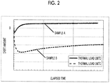
- FIG. 2 shows the behaviors of the drift phenomenon when a constant voltage is applied at 85°C to the two samples A and B.
- Non Patent Literature No. 1 "A Review of Lithium Niobate Modulators for Fiber-Optic Communications Systems", IEEE Journal of Selected Topics in Quantum Electronics, Vol. 6, No. 1, pp 69 (2000 )
- An object of the invention is to solve the above-described problems, and to provide an optical element in which an electrode is directly formed on an LN substrate, and a drift phenomenon is suppressed.
- an optical element of the invention has the following technical features.
- an optical element including: a substrate made of lithium niobate crystals; and an electrode disposed on the substrate, the substrate and the electrode are in direct contact with each other, and as a contact metal disposed on a surface of the electrode where the electrode is in contact with the substrate, a metal material whose standard enthalpy of formation per coordinate bond upon oxidation is greater than a standard enthalpy of formation per coordinate bond of niobium pentoxide is used. Accordingly, it is possible to provide an optical element in which a drift phenomenon is suppressed.
- an optical element including: a substrate made of lithium niobate crystals; and an electrode disposed on the substrate, the substrate and the electrode are in direct contact with each other, and as a contact metal disposed on a surface of the electrode where the electrode is in contact with the substrate, an oxide conductor is used. Accordingly, it is possible to provide an optical element in which a drift phenomenon is suppressed.
- the inventors have conducted intensive studies, and as a result, found that in a case where an electrode is directly formed on an LN substrate, the metal in contact with the substrate takes oxygen in the substrate and causes oxygen deficiency in the LN substrate, and a drift phenomenon thus occurs, and made the invention.
- an optical element including a substrate made of lithium niobate crystals and an electrode disposed on the substrate, in which the substrate and the electrode are in direct contact with each other, and as a contact metal disposed on a surface of the electrode where the electrode is in contact with the substrate, a metal material whose standard enthalpy of formation per coordinate bond upon oxidation is greater than a standard enthalpy of formation per coordinate bond of niobium pentoxide is used.
- any one of Co, Ni, Mo, W, and V is preferably used as the contact metal.
- a ratio of a depth of an oxygen-deficient region to the thickness of the substrate is high, whereby a drift phenomenon more significantly occurs. Accordingly, in a case where an LN substrate having a thickness of 20 ⁇ m or less is used, the invention is expected to more effectively exert its effects.
- the metal (contact metal) in direct contact with the LN substrate in a case where a material such as Ni or W whose standard enthalpy of formation per coordinate bond upon oxidation is greater than that of Nb 2 O 5 is used as the contact metal instead of Ti or Cr according to the related art, deprivation of the oxygen in the LN substrate by the contact metal can be suppressed, and a reduction in the electric resistance near the interface between the contact metal and the LN substrate can be suppressed. Accordingly, suppression of a change with the lapse of time in the amount of oxygen deficiency at the interface between the contact metal and the LN substrate and a high resistance of the LN substrate are maintained. As a result, a drift amount of the optical element such as an LN modulator is reduced, and a change of the drift phenomenon due to heat is suppressed.
- Table 1 shows a list of standard enthalpies of formation of metal oxides corresponding to the bonding energies of metals and oxygen. The lower in Table 1, the easier the bonding of a metal to oxygen. Accordingly, in order to suppress oxygen deficiency in the LN substrate, a metal positioned above Nb 2 O 5 in Table 1 is preferably selected as the contact metal.
- Ag, Pd, Rh, and Cu have low adhesiveness to the LN substrate, and are not suitable as the contact metal.
- Sb and Ba should not be used since these have toxicity (or are suspected to be toxic substances) .
- Fe has an extremely high magnetic permeability and increases microwave loss, and thus it is not suitable for a modulation electrode (control electrode) of an optical modulator or the like.
- Bi, Sn, and In have a low melting point, and thus a maximum temperature of the manufacturing process is limited. Therefore, these are not suitable for use in the manufacturing process.
- Ge is poor in deliquescence or the like. Zn is likely to form an alloy with other metals, and thus a problem occurs in the process design.
- the contact metal in contact with the substrate the "metal material whose standard enthalpy of formation per coordinate bond upon oxidation is greater than a standard enthalpy of formation per coordinate bond of niobium pentoxide" has been described, but the contact metal is not limited to the above metal material.
- An “oxide conductor” can also be used. Since the oxide conductor is a metal material that has already been oxidized, it does not deprive oxygen from the LN substrate. Accordingly, in a case where the oxide conductor is used as the contact metal, DC drift is suppressed. Examples of the oxide conductor include indium tin oxide (ITO), RuO 2 , and IrO 2 .
- a second test was performed using Al as a contact metal, and a third test was performed using Ni as a contact metal. Basically, the second and third tests are performed under the same conditions, except that the material of the contact metal is changed.
- a contact metal film was formed on the X-cut LN substrate in which the Ti-diffused waveguide was formed.
- 50 nm of an Au film was sequentially accumulated on the contact metal film by vacuum deposition.
- a control electrode electrode length: 40 mm, inter-electrode distance: 25 ⁇ m
- a thickness of 3 ⁇ m is formed by photolithography and electrolytic gold plating.
- an LN modulator shown in a plan view of FIG. 3A and a cross-sectional view of FIG. 3B was made.
- Al is used as a contact metal
- Ti thickness: 100 nm
- Ti is inserted between Al and Au in order to suppress an alloy reaction between Al and Au due to a thermal load (see FIG. 3B ) .
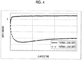
- FIGS. 3A and 3B An LN modulator provided as shown in FIGS. 3A and 3B and subjected to a thermal load at 200°C for 1 hour without the application of a voltage before measurement, and an LN modulator provided as shown in FIGS. 3A and 3B and subjected to a thermal load at 280°C for 1 hour without the application of a voltage before measurement were prepared. Evaluation results of a drift phenomenon occurring when a constant voltage is applied (an 8 V voltage is applied) to the LN modulator at 85°C are shown in FIG. 4 .
- an LN modulator using Ni as a contact metal was made.
- An Au film between electrodes and a Ni film of the contact metal are removed by chemical etching or the like.
- An iodine-potassium iodide aqueous solution is preferably used as an etching solution for the Au film, and a dilute nitric acid or the like is preferably used as an etching solution for the Ni film.
- the LN modulator used in the third test is shown in a plan view of FIG. 5A and a cross-sectional view of FIG. 5B .
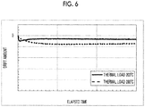
- FIGS. 5A and 5B An LN modulator provided as shown in FIGS. 5A and 5B and subjected to a thermal load at 200°C for 1 hour without the application of a voltage before measurement, and an LN modulator provided as shown in FIGS. 5A and 5B and subjected to a thermal load at 280°C for 1 hour without the application of a voltage before measurement were prepared. Evaluation results of a drift phenomenon occurring when a constant voltage is applied (an 8 V voltage is applied) to the LN modulator at 85°C are shown in FIG. 6 . As shown in FIG. 6 , in a case where Ni was used as a contact metal, changes due to the thermal load were rarely shown in the drift phenomenon.
- the drift phenomenon changes by the contact metal in the LN modulator in which the electrode is directly formed on the LN substrate. Moreover, it is presumed that the contact metal takes oxygen from the LN substrate and causes oxygen deficiency in the LN substrate, and as a result, the drift phenomenon changes due to the thermal load before measurement.
- a guard electrode is disposed along an outer periphery of an LN substrate as shown in a plan view of FIG. 7A and a cross-sectional view of FIG. 7B , and electrodes having a comb-like structure (electrodes A and B) are provided.
- electrodes A and B electrodes having a comb-like structure
- FIG. 7A comb-like electrodes having an electrode length of 10 mm and an inter-electrode distance of 15 ⁇ m are formed, and electrodes A and B are separated from the ground electrode at the outer periphery by 100 ⁇ m or more.
- 100 nm of a contact metal Ti is formed on the LN substrate, and 4 ⁇ m of an Au plating is formed on an upper surface of the contact metal Ti.
- a desired voltage is applied to the electrode A, and the voltage of the electrode B is set to 0V.
- a current flowing through the electrode B at this time is evaluated.
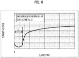
- FIG. 8 An example of the measurement results is shown in FIG. 8 .
- the voltage applied to the electrode A is 60V.
- a change with the lapse of time in the conductivity (reciprocal of resistance) of the LN substrate under air atmosphere is measured.
- the current does not flow so much at the beginning of the voltage application, but the current suddenly starts to flow at a certain time.
- the double-headed arrow portion shown in FIG. 8 is defined as a "current rise time (T L )".
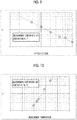
- FIG. 9 shows results of examination of the relationship between the current rise time (T L ) and the applied voltage.
- FIG. 9 is a double logarithmic chart, and it is found that the measurement results are on a straight line.
- FIG. 10 shows results of examination of temperature (T) dependence at a fixed applied voltage.
- FIG. 10 is a single logarithmic chart, and the relationship between T L and a temperature (T) follows the Arrhenius equation. That is, in a case where Ti is used as a contact metal, T L follows the Eyring' s model represented by Expression 1.
- T L AV " exp E a k B T (E a : activation energy, k B : Boltzmann constant, A, n: constant)
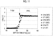
- FIG. 11 shows results of Auger electron spectroscopy (AES) analysis of the three samples in a depth direction from the Ti film to the LN substrate.
- AES Auger electron spectroscopy
Landscapes
- Physics & Mathematics (AREA)
- Nonlinear Science (AREA)
- Chemical & Material Sciences (AREA)
- Engineering & Computer Science (AREA)
- Ceramic Engineering (AREA)
- Crystallography & Structural Chemistry (AREA)
- General Physics & Mathematics (AREA)
- Optics & Photonics (AREA)
- Optical Modulation, Optical Deflection, Nonlinear Optics, Optical Demodulation, Optical Logic Elements (AREA)
Applications Claiming Priority (2)
| Application Number | Priority Date | Filing Date | Title |
|---|---|---|---|
| JP2018065082A JP7052487B2 (ja) | 2018-03-29 | 2018-03-29 | 光素子 |
| PCT/JP2019/007615 WO2019187932A1 (ja) | 2018-03-29 | 2019-02-27 | 光素子 |
Publications (3)
| Publication Number | Publication Date |
|---|---|
| EP3779574A1 true EP3779574A1 (de) | 2021-02-17 |
| EP3779574A4 EP3779574A4 (de) | 2021-12-15 |
| EP3779574B1 EP3779574B1 (de) | 2024-01-17 |
Family
ID=68061195
Family Applications (1)
| Application Number | Title | Priority Date | Filing Date |
|---|---|---|---|
| EP19776059.8A Active EP3779574B1 (de) | 2018-03-29 | 2019-02-27 | Optisches element |
Country Status (5)
| Country | Link |
|---|---|
| US (1) | US11347086B2 (de) |
| EP (1) | EP3779574B1 (de) |
| JP (1) | JP7052487B2 (de) |
| CN (1) | CN111936917B (de) |
| WO (1) | WO2019187932A1 (de) |
Families Citing this family (2)
| Publication number | Priority date | Publication date | Assignee | Title |
|---|---|---|---|---|
| EP4474887A4 (de) | 2022-01-31 | 2025-11-26 | Sumitomo Osaka Cement Co Ltd | Optisches wellenleiterelement und optische modulationsvorrichtung und optische übertragungsvorrichtung damit |
| CN116794861A (zh) * | 2022-03-17 | 2023-09-22 | Tdk株式会社 | 光调制元件 |
Family Cites Families (22)
| Publication number | Priority date | Publication date | Assignee | Title |
|---|---|---|---|---|
| JP2798350B2 (ja) | 1993-11-30 | 1998-09-17 | 住友大阪セメント株式会社 | 直流電圧のドリフトが制御されている導波路型電気光学素子の選別方法 |
| JP3954192B2 (ja) | 1998-03-12 | 2007-08-08 | 日本碍子株式会社 | 光導波路素子およびその製造方法 |
| JP3303820B2 (ja) | 1999-02-04 | 2002-07-22 | 日本電気株式会社 | 導波路型光デバイス製造方法 |
| JP4401531B2 (ja) | 2000-05-01 | 2010-01-20 | 住友大阪セメント株式会社 | 微細パターン電極の形成方法および光素子 |
| EP1258772A1 (de) | 2001-05-14 | 2002-11-20 | Corning O.T.I. S.p.A. | Elektrooptischer Modulator mit hoher Bandbreite und niedriger Steuerspannung |
| JP4968995B2 (ja) * | 2001-08-22 | 2012-07-04 | 住友大阪セメント株式会社 | 光変調器 |
| US20030062551A1 (en) | 2001-10-02 | 2003-04-03 | Jds Uniphase Corporation | Electrode structure including encapsulated adhesion layer |
| JP4375597B2 (ja) * | 2001-11-16 | 2009-12-02 | 日本碍子株式会社 | 光導波路デバイスおよび進行波形光変調器 |
| US6867134B2 (en) | 2002-03-20 | 2005-03-15 | Jds Uniphase Corporation | Adherent all-gold electrode structure for lithium niobate based devices and the method of fabrication |
| JP4936838B2 (ja) * | 2005-09-29 | 2012-05-23 | 住友大阪セメント株式会社 | 光制御デバイス |
| JP2007272122A (ja) * | 2006-03-31 | 2007-10-18 | Sumitomo Osaka Cement Co Ltd | 光制御素子 |
| US7529433B2 (en) * | 2007-01-12 | 2009-05-05 | Jds Uniphase Corporation | Humidity tolerant electro-optic device |
| WO2009022360A1 (en) * | 2007-08-14 | 2009-02-19 | Selex Sistemi Integrati S.P.A. | Low switching voltage, fast time response digital optical switch |
| EP2317562A1 (de) * | 2009-11-03 | 2011-05-04 | Fundacio Privada Institut De Ciencies Fotoniques | Mehrschichtige Metallelektroden für Optoelektronik |
| US8070368B1 (en) | 2010-07-20 | 2011-12-06 | L-3 Communications Corporation | Hermetically packaged LiNbO3 optical circuit with oxidizing fill gas |
| JP2013210568A (ja) | 2012-03-30 | 2013-10-10 | Sumitomo Osaka Cement Co Ltd | 光変調器 |
| TWI572917B (zh) | 2013-02-04 | 2017-03-01 | 鴻海精密工業股份有限公司 | 極化分離器 |
| US9020306B2 (en) * | 2013-03-14 | 2015-04-28 | The Aerospace Corporation | Stable lithium niobate waveguide devices, and methods of making and using same |
| JP6325811B2 (ja) | 2013-12-25 | 2018-05-16 | 住友大阪セメント株式会社 | 光制御デバイス |
| JP2016071250A (ja) | 2014-09-30 | 2016-05-09 | 住友大阪セメント株式会社 | 電極付き基板 |
| CN105022178B (zh) * | 2015-08-18 | 2018-04-03 | 电子科技大学 | 基于平面波导的石墨烯相位型光调制器 |
| KR102698290B1 (ko) | 2016-09-09 | 2024-08-23 | 삼성전자주식회사 | 위상 변조 능동 소자, 이의 구동 방법 및 위상 변조 능동 소자를 포함하는 광학 장치 |
-
2018
- 2018-03-29 JP JP2018065082A patent/JP7052487B2/ja active Active
-
2019
- 2019-02-27 WO PCT/JP2019/007615 patent/WO2019187932A1/ja not_active Ceased
- 2019-02-27 EP EP19776059.8A patent/EP3779574B1/de active Active
- 2019-02-27 CN CN201980023012.7A patent/CN111936917B/zh active Active
- 2019-02-27 US US17/042,839 patent/US11347086B2/en active Active
Also Published As
| Publication number | Publication date |
|---|---|
| EP3779574B1 (de) | 2024-01-17 |
| JP7052487B2 (ja) | 2022-04-12 |
| US20210026165A1 (en) | 2021-01-28 |
| EP3779574A4 (de) | 2021-12-15 |
| CN111936917B (zh) | 2024-10-01 |
| JP2019174733A (ja) | 2019-10-10 |
| WO2019187932A1 (ja) | 2019-10-03 |
| US11347086B2 (en) | 2022-05-31 |
| CN111936917A (zh) | 2020-11-13 |
Similar Documents
| Publication | Publication Date | Title |
|---|---|---|
| US10698286B2 (en) | Electrochromic multi-layer devices with charge sequestration and related methods | |
| Hossein-Babaei et al. | Electronic conduction in Ti/poly-TiO2/Ti structures | |
| EP3309541B1 (de) | Messelement für eine ionensensitive festkontakt-elektrode und ionensensitive festkontakt-elektrode | |
| EP3779574B1 (de) | Optisches element | |
| GB1502340A (en) | Controllable electrochromic display cell | |
| DE3736075A1 (de) | Elektrochromes schichtenpaket | |
| US20220373849A1 (en) | Transparent thermoelectric selfpowered glazing | |
| EP3798718A1 (de) | Verbundsubstrat für elektro-optisches element und verfahren zu dessen herstellung | |
| US4225216A (en) | Tungsten niobate electrochromic device | |
| JP5072232B2 (ja) | バイアス点直流電圧ドリフトおよび熱偏移抑制式の電気光学導波路素子とその製造方法 | |
| US11988935B2 (en) | Bus bar design of an IGU with graded transmission state | |
| JP4200221B2 (ja) | 可逆着脱色固体素子、可逆導電性変化固体素子、可逆屈折率変化固体素子、非発光型表示素子、通電路素子および光導波路素子 | |
| US12092936B2 (en) | Porous perovskite nickelates with enhanced electrochromic properties and systems thereof | |
| US20220121077A1 (en) | Electrochromic device including a means for mechanical resistance and a process of forming the same | |
| US20230004058A1 (en) | Thermal tempering of a working electrode | |
| US20100014145A1 (en) | Electrode comprising lithium nickel oxide layer, method for preparing the same, and electrochromic device comprising the same | |
| US20200326603A1 (en) | Apparatus for operating an electroactive device and a method of using the same | |
| KR102856938B1 (ko) | 절연층이 삽입된 광 투과가변 소자 | |
| JPS5953816A (ja) | 全固体型エレクトロクロミツク素子 | |
| Dodin et al. | Electrical transport in silver phosphate glasses containing V2O5 and MoO3 | |
| Holloway et al. | Electrically Controlled Coloration of Materials. | |
| JPS5895328A (ja) | エレクトロクロミツク表示装置 |
Legal Events
| Date | Code | Title | Description |
|---|---|---|---|
| STAA | Information on the status of an ep patent application or granted ep patent |
Free format text: STATUS: THE INTERNATIONAL PUBLICATION HAS BEEN MADE |
|
| PUAI | Public reference made under article 153(3) epc to a published international application that has entered the european phase |
Free format text: ORIGINAL CODE: 0009012 |
|
| STAA | Information on the status of an ep patent application or granted ep patent |
Free format text: STATUS: REQUEST FOR EXAMINATION WAS MADE |
|
| 17P | Request for examination filed |
Effective date: 20200929 |
|
| AK | Designated contracting states |
Kind code of ref document: A1 Designated state(s): AL AT BE BG CH CY CZ DE DK EE ES FI FR GB GR HR HU IE IS IT LI LT LU LV MC MK MT NL NO PL PT RO RS SE SI SK SM TR |
|
| AX | Request for extension of the european patent |
Extension state: BA ME |
|
| DAV | Request for validation of the european patent (deleted) | ||
| DAX | Request for extension of the european patent (deleted) | ||
| A4 | Supplementary search report drawn up and despatched |
Effective date: 20211112 |
|
| RIC1 | Information provided on ipc code assigned before grant |
Ipc: G02F 1/035 20060101ALI20211108BHEP Ipc: G02F 1/03 20060101AFI20211108BHEP |
|
| GRAP | Despatch of communication of intention to grant a patent |
Free format text: ORIGINAL CODE: EPIDOSNIGR1 |
|
| STAA | Information on the status of an ep patent application or granted ep patent |
Free format text: STATUS: GRANT OF PATENT IS INTENDED |
|
| INTG | Intention to grant announced |
Effective date: 20230927 |
|
| RAP3 | Party data changed (applicant data changed or rights of an application transferred) |
Owner name: SUMITOMO OSAKA CEMENT CO., LTD. |
|
| GRAS | Grant fee paid |
Free format text: ORIGINAL CODE: EPIDOSNIGR3 |
|
| GRAA | (expected) grant |
Free format text: ORIGINAL CODE: 0009210 |
|
| STAA | Information on the status of an ep patent application or granted ep patent |
Free format text: STATUS: THE PATENT HAS BEEN GRANTED |
|
| AK | Designated contracting states |
Kind code of ref document: B1 Designated state(s): AL AT BE BG CH CY CZ DE DK EE ES FI FR GB GR HR HU IE IS IT LI LT LU LV MC MK MT NL NO PL PT RO RS SE SI SK SM TR |
|
| REG | Reference to a national code |
Ref country code: GB Ref legal event code: FG4D |
|
| REG | Reference to a national code |
Ref country code: CH Ref legal event code: EP |
|
| REG | Reference to a national code |
Ref country code: DE Ref legal event code: R096 Ref document number: 602019045254 Country of ref document: DE |
|
| REG | Reference to a national code |
Ref country code: IE Ref legal event code: FG4D |
|
| REG | Reference to a national code |
Ref country code: LT Ref legal event code: MG9D |
|
| REG | Reference to a national code |
Ref country code: NL Ref legal event code: MP Effective date: 20240117 |
|
| REG | Reference to a national code |
Ref country code: AT Ref legal event code: MK05 Ref document number: 1650920 Country of ref document: AT Kind code of ref document: T Effective date: 20240117 |
|
| PG25 | Lapsed in a contracting state [announced via postgrant information from national office to epo] |
Ref country code: NL Free format text: LAPSE BECAUSE OF FAILURE TO SUBMIT A TRANSLATION OF THE DESCRIPTION OR TO PAY THE FEE WITHIN THE PRESCRIBED TIME-LIMIT Effective date: 20240117 |
|
| PG25 | Lapsed in a contracting state [announced via postgrant information from national office to epo] |
Ref country code: NL Free format text: LAPSE BECAUSE OF FAILURE TO SUBMIT A TRANSLATION OF THE DESCRIPTION OR TO PAY THE FEE WITHIN THE PRESCRIBED TIME-LIMIT Effective date: 20240117 |
|
| PG25 | Lapsed in a contracting state [announced via postgrant information from national office to epo] |
Ref country code: IS Free format text: LAPSE BECAUSE OF FAILURE TO SUBMIT A TRANSLATION OF THE DESCRIPTION OR TO PAY THE FEE WITHIN THE PRESCRIBED TIME-LIMIT Effective date: 20240517 |
|
| PG25 | Lapsed in a contracting state [announced via postgrant information from national office to epo] |
Ref country code: LT Free format text: LAPSE BECAUSE OF FAILURE TO SUBMIT A TRANSLATION OF THE DESCRIPTION OR TO PAY THE FEE WITHIN THE PRESCRIBED TIME-LIMIT Effective date: 20240117 |
|
| PG25 | Lapsed in a contracting state [announced via postgrant information from national office to epo] |
Ref country code: GR Free format text: LAPSE BECAUSE OF FAILURE TO SUBMIT A TRANSLATION OF THE DESCRIPTION OR TO PAY THE FEE WITHIN THE PRESCRIBED TIME-LIMIT Effective date: 20240418 |
|
| PG25 | Lapsed in a contracting state [announced via postgrant information from national office to epo] |
Ref country code: RS Free format text: LAPSE BECAUSE OF FAILURE TO SUBMIT A TRANSLATION OF THE DESCRIPTION OR TO PAY THE FEE WITHIN THE PRESCRIBED TIME-LIMIT Effective date: 20240417 Ref country code: HR Free format text: LAPSE BECAUSE OF FAILURE TO SUBMIT A TRANSLATION OF THE DESCRIPTION OR TO PAY THE FEE WITHIN THE PRESCRIBED TIME-LIMIT Effective date: 20240117 |
|
| PG25 | Lapsed in a contracting state [announced via postgrant information from national office to epo] |
Ref country code: ES Free format text: LAPSE BECAUSE OF FAILURE TO SUBMIT A TRANSLATION OF THE DESCRIPTION OR TO PAY THE FEE WITHIN THE PRESCRIBED TIME-LIMIT Effective date: 20240117 |
|
| PG25 | Lapsed in a contracting state [announced via postgrant information from national office to epo] |
Ref country code: AT Free format text: LAPSE BECAUSE OF FAILURE TO SUBMIT A TRANSLATION OF THE DESCRIPTION OR TO PAY THE FEE WITHIN THE PRESCRIBED TIME-LIMIT Effective date: 20240117 |
|
| PG25 | Lapsed in a contracting state [announced via postgrant information from national office to epo] |
Ref country code: RS Free format text: LAPSE BECAUSE OF FAILURE TO SUBMIT A TRANSLATION OF THE DESCRIPTION OR TO PAY THE FEE WITHIN THE PRESCRIBED TIME-LIMIT Effective date: 20240417 Ref country code: NO Free format text: LAPSE BECAUSE OF FAILURE TO SUBMIT A TRANSLATION OF THE DESCRIPTION OR TO PAY THE FEE WITHIN THE PRESCRIBED TIME-LIMIT Effective date: 20240417 Ref country code: LT Free format text: LAPSE BECAUSE OF FAILURE TO SUBMIT A TRANSLATION OF THE DESCRIPTION OR TO PAY THE FEE WITHIN THE PRESCRIBED TIME-LIMIT Effective date: 20240117 Ref country code: IS Free format text: LAPSE BECAUSE OF FAILURE TO SUBMIT A TRANSLATION OF THE DESCRIPTION OR TO PAY THE FEE WITHIN THE PRESCRIBED TIME-LIMIT Effective date: 20240517 Ref country code: HR Free format text: LAPSE BECAUSE OF FAILURE TO SUBMIT A TRANSLATION OF THE DESCRIPTION OR TO PAY THE FEE WITHIN THE PRESCRIBED TIME-LIMIT Effective date: 20240117 Ref country code: GR Free format text: LAPSE BECAUSE OF FAILURE TO SUBMIT A TRANSLATION OF THE DESCRIPTION OR TO PAY THE FEE WITHIN THE PRESCRIBED TIME-LIMIT Effective date: 20240418 Ref country code: FI Free format text: LAPSE BECAUSE OF FAILURE TO SUBMIT A TRANSLATION OF THE DESCRIPTION OR TO PAY THE FEE WITHIN THE PRESCRIBED TIME-LIMIT Effective date: 20240117 Ref country code: ES Free format text: LAPSE BECAUSE OF FAILURE TO SUBMIT A TRANSLATION OF THE DESCRIPTION OR TO PAY THE FEE WITHIN THE PRESCRIBED TIME-LIMIT Effective date: 20240117 Ref country code: BG Free format text: LAPSE BECAUSE OF FAILURE TO SUBMIT A TRANSLATION OF THE DESCRIPTION OR TO PAY THE FEE WITHIN THE PRESCRIBED TIME-LIMIT Effective date: 20240117 Ref country code: AT Free format text: LAPSE BECAUSE OF FAILURE TO SUBMIT A TRANSLATION OF THE DESCRIPTION OR TO PAY THE FEE WITHIN THE PRESCRIBED TIME-LIMIT Effective date: 20240117 |
|
| PG25 | Lapsed in a contracting state [announced via postgrant information from national office to epo] |
Ref country code: PL Free format text: LAPSE BECAUSE OF FAILURE TO SUBMIT A TRANSLATION OF THE DESCRIPTION OR TO PAY THE FEE WITHIN THE PRESCRIBED TIME-LIMIT Effective date: 20240117 Ref country code: PT Free format text: LAPSE BECAUSE OF FAILURE TO SUBMIT A TRANSLATION OF THE DESCRIPTION OR TO PAY THE FEE WITHIN THE PRESCRIBED TIME-LIMIT Effective date: 20240517 |
|
| PG25 | Lapsed in a contracting state [announced via postgrant information from national office to epo] |
Ref country code: SE Free format text: LAPSE BECAUSE OF FAILURE TO SUBMIT A TRANSLATION OF THE DESCRIPTION OR TO PAY THE FEE WITHIN THE PRESCRIBED TIME-LIMIT Effective date: 20240117 Ref country code: PT Free format text: LAPSE BECAUSE OF FAILURE TO SUBMIT A TRANSLATION OF THE DESCRIPTION OR TO PAY THE FEE WITHIN THE PRESCRIBED TIME-LIMIT Effective date: 20240517 Ref country code: PL Free format text: LAPSE BECAUSE OF FAILURE TO SUBMIT A TRANSLATION OF THE DESCRIPTION OR TO PAY THE FEE WITHIN THE PRESCRIBED TIME-LIMIT Effective date: 20240117 Ref country code: LV Free format text: LAPSE BECAUSE OF FAILURE TO SUBMIT A TRANSLATION OF THE DESCRIPTION OR TO PAY THE FEE WITHIN THE PRESCRIBED TIME-LIMIT Effective date: 20240117 |
|
| REG | Reference to a national code |
Ref country code: CH Ref legal event code: PL |
|
| PG25 | Lapsed in a contracting state [announced via postgrant information from national office to epo] |
Ref country code: DK Free format text: LAPSE BECAUSE OF FAILURE TO SUBMIT A TRANSLATION OF THE DESCRIPTION OR TO PAY THE FEE WITHIN THE PRESCRIBED TIME-LIMIT Effective date: 20240117 |
|
| PG25 | Lapsed in a contracting state [announced via postgrant information from national office to epo] |
Ref country code: SM Free format text: LAPSE BECAUSE OF FAILURE TO SUBMIT A TRANSLATION OF THE DESCRIPTION OR TO PAY THE FEE WITHIN THE PRESCRIBED TIME-LIMIT Effective date: 20240117 |
|
| PG25 | Lapsed in a contracting state [announced via postgrant information from national office to epo] |
Ref country code: LU Free format text: LAPSE BECAUSE OF NON-PAYMENT OF DUE FEES Effective date: 20240227 |
|
| REG | Reference to a national code |
Ref country code: DE Ref legal event code: R097 Ref document number: 602019045254 Country of ref document: DE |
|
| PG25 | Lapsed in a contracting state [announced via postgrant information from national office to epo] |
Ref country code: CH Free format text: LAPSE BECAUSE OF NON-PAYMENT OF DUE FEES Effective date: 20240229 |
|
| PG25 | Lapsed in a contracting state [announced via postgrant information from national office to epo] |
Ref country code: EE Free format text: LAPSE BECAUSE OF FAILURE TO SUBMIT A TRANSLATION OF THE DESCRIPTION OR TO PAY THE FEE WITHIN THE PRESCRIBED TIME-LIMIT Effective date: 20240117 Ref country code: CZ Free format text: LAPSE BECAUSE OF FAILURE TO SUBMIT A TRANSLATION OF THE DESCRIPTION OR TO PAY THE FEE WITHIN THE PRESCRIBED TIME-LIMIT Effective date: 20240117 |
|
| PG25 | Lapsed in a contracting state [announced via postgrant information from national office to epo] |
Ref country code: SK Free format text: LAPSE BECAUSE OF FAILURE TO SUBMIT A TRANSLATION OF THE DESCRIPTION OR TO PAY THE FEE WITHIN THE PRESCRIBED TIME-LIMIT Effective date: 20240117 |
|
| PG25 | Lapsed in a contracting state [announced via postgrant information from national office to epo] |
Ref country code: SM Free format text: LAPSE BECAUSE OF FAILURE TO SUBMIT A TRANSLATION OF THE DESCRIPTION OR TO PAY THE FEE WITHIN THE PRESCRIBED TIME-LIMIT Effective date: 20240117 Ref country code: SK Free format text: LAPSE BECAUSE OF FAILURE TO SUBMIT A TRANSLATION OF THE DESCRIPTION OR TO PAY THE FEE WITHIN THE PRESCRIBED TIME-LIMIT Effective date: 20240117 Ref country code: RO Free format text: LAPSE BECAUSE OF FAILURE TO SUBMIT A TRANSLATION OF THE DESCRIPTION OR TO PAY THE FEE WITHIN THE PRESCRIBED TIME-LIMIT Effective date: 20240117 Ref country code: LU Free format text: LAPSE BECAUSE OF NON-PAYMENT OF DUE FEES Effective date: 20240227 Ref country code: EE Free format text: LAPSE BECAUSE OF FAILURE TO SUBMIT A TRANSLATION OF THE DESCRIPTION OR TO PAY THE FEE WITHIN THE PRESCRIBED TIME-LIMIT Effective date: 20240117 Ref country code: DK Free format text: LAPSE BECAUSE OF FAILURE TO SUBMIT A TRANSLATION OF THE DESCRIPTION OR TO PAY THE FEE WITHIN THE PRESCRIBED TIME-LIMIT Effective date: 20240117 Ref country code: CZ Free format text: LAPSE BECAUSE OF FAILURE TO SUBMIT A TRANSLATION OF THE DESCRIPTION OR TO PAY THE FEE WITHIN THE PRESCRIBED TIME-LIMIT Effective date: 20240117 Ref country code: CH Free format text: LAPSE BECAUSE OF NON-PAYMENT OF DUE FEES Effective date: 20240229 |
|
| PG25 | Lapsed in a contracting state [announced via postgrant information from national office to epo] |
Ref country code: MC Free format text: LAPSE BECAUSE OF FAILURE TO SUBMIT A TRANSLATION OF THE DESCRIPTION OR TO PAY THE FEE WITHIN THE PRESCRIBED TIME-LIMIT Effective date: 20240117 |
|
| PLBE | No opposition filed within time limit |
Free format text: ORIGINAL CODE: 0009261 |
|
| STAA | Information on the status of an ep patent application or granted ep patent |
Free format text: STATUS: NO OPPOSITION FILED WITHIN TIME LIMIT |
|
| PG25 | Lapsed in a contracting state [announced via postgrant information from national office to epo] |
Ref country code: MC Free format text: LAPSE BECAUSE OF FAILURE TO SUBMIT A TRANSLATION OF THE DESCRIPTION OR TO PAY THE FEE WITHIN THE PRESCRIBED TIME-LIMIT Effective date: 20240117 |
|
| REG | Reference to a national code |
Ref country code: BE Ref legal event code: MM Effective date: 20240229 |
|
| 26N | No opposition filed |
Effective date: 20241018 |
|
| GBPC | Gb: european patent ceased through non-payment of renewal fee |
Effective date: 20240417 |
|
| PG25 | Lapsed in a contracting state [announced via postgrant information from national office to epo] |
Ref country code: BE Free format text: LAPSE BECAUSE OF NON-PAYMENT OF DUE FEES Effective date: 20240229 |
|
| PG25 | Lapsed in a contracting state [announced via postgrant information from national office to epo] |
Ref country code: GB Free format text: LAPSE BECAUSE OF NON-PAYMENT OF DUE FEES Effective date: 20240417 |
|
| PG25 | Lapsed in a contracting state [announced via postgrant information from national office to epo] |
Ref country code: FR Free format text: LAPSE BECAUSE OF NON-PAYMENT OF DUE FEES Effective date: 20240317 |
|
| PG25 | Lapsed in a contracting state [announced via postgrant information from national office to epo] |
Ref country code: IE Free format text: LAPSE BECAUSE OF NON-PAYMENT OF DUE FEES Effective date: 20240227 |
|
| PG25 | Lapsed in a contracting state [announced via postgrant information from national office to epo] |
Ref country code: IE Free format text: LAPSE BECAUSE OF NON-PAYMENT OF DUE FEES Effective date: 20240227 Ref country code: GB Free format text: LAPSE BECAUSE OF NON-PAYMENT OF DUE FEES Effective date: 20240417 Ref country code: FR Free format text: LAPSE BECAUSE OF NON-PAYMENT OF DUE FEES Effective date: 20240317 Ref country code: BE Free format text: LAPSE BECAUSE OF NON-PAYMENT OF DUE FEES Effective date: 20240229 |
|
| PG25 | Lapsed in a contracting state [announced via postgrant information from national office to epo] |
Ref country code: SI Free format text: LAPSE BECAUSE OF FAILURE TO SUBMIT A TRANSLATION OF THE DESCRIPTION OR TO PAY THE FEE WITHIN THE PRESCRIBED TIME-LIMIT Effective date: 20240117 |
|
| PG25 | Lapsed in a contracting state [announced via postgrant information from national office to epo] |
Ref country code: CY Free format text: LAPSE BECAUSE OF FAILURE TO SUBMIT A TRANSLATION OF THE DESCRIPTION OR TO PAY THE FEE WITHIN THE PRESCRIBED TIME-LIMIT; INVALID AB INITIO Effective date: 20190227 |
|
| PG25 | Lapsed in a contracting state [announced via postgrant information from national office to epo] |
Ref country code: HU Free format text: LAPSE BECAUSE OF FAILURE TO SUBMIT A TRANSLATION OF THE DESCRIPTION OR TO PAY THE FEE WITHIN THE PRESCRIBED TIME-LIMIT; INVALID AB INITIO Effective date: 20190227 |
|
| PG25 | Lapsed in a contracting state [announced via postgrant information from national office to epo] |
Ref country code: TR Free format text: LAPSE BECAUSE OF FAILURE TO SUBMIT A TRANSLATION OF THE DESCRIPTION OR TO PAY THE FEE WITHIN THE PRESCRIBED TIME-LIMIT Effective date: 20240117 |
|
| PGFP | Annual fee paid to national office [announced via postgrant information from national office to epo] |
Ref country code: DE Payment date: 20260218 Year of fee payment: 8 |
|
| PGFP | Annual fee paid to national office [announced via postgrant information from national office to epo] |
Ref country code: IT Payment date: 20260224 Year of fee payment: 8 |