EP3779577B1 - Dimmelement mit glasfilm - Google Patents
Dimmelement mit glasfilm Download PDFInfo
- Publication number
- EP3779577B1 EP3779577B1 EP19775974.9A EP19775974A EP3779577B1 EP 3779577 B1 EP3779577 B1 EP 3779577B1 EP 19775974 A EP19775974 A EP 19775974A EP 3779577 B1 EP3779577 B1 EP 3779577B1
- Authority
- EP
- European Patent Office
- Prior art keywords
- layer
- light control
- film
- control element
- thickness
- Prior art date
- Legal status (The legal status is an assumption and is not a legal conclusion. Google has not performed a legal analysis and makes no representation as to the accuracy of the status listed.)
- Active
Links
Images

Classifications
-
- B—PERFORMING OPERATIONS; TRANSPORTING
- B32—LAYERED PRODUCTS
- B32B—LAYERED PRODUCTS, i.e. PRODUCTS BUILT-UP OF STRATA OF FLAT OR NON-FLAT, e.g. CELLULAR OR HONEYCOMB, FORM
- B32B17/00—Layered products essentially comprising sheet glass, or glass, slag, or like fibres
- B32B17/06—Layered products essentially comprising sheet glass, or glass, slag, or like fibres comprising glass as the main or only constituent of a layer, next to another layer of a specific material
- B32B17/10—Layered products essentially comprising sheet glass, or glass, slag, or like fibres comprising glass as the main or only constituent of a layer, next to another layer of a specific material of synthetic resin
- B32B17/10005—Layered products essentially comprising sheet glass, or glass, slag, or like fibres comprising glass as the main or only constituent of a layer, next to another layer of a specific material of synthetic resin laminated safety glass or glazing
- B32B17/10807—Making laminated safety glass or glazing; Apparatus therefor
-
- C—CHEMISTRY; METALLURGY
- C09—DYES; PAINTS; POLISHES; NATURAL RESINS; ADHESIVES; COMPOSITIONS NOT OTHERWISE PROVIDED FOR; APPLICATIONS OF MATERIALS NOT OTHERWISE PROVIDED FOR
- C09J—ADHESIVES; NON-MECHANICAL ASPECTS OF ADHESIVE PROCESSES IN GENERAL; ADHESIVE PROCESSES NOT PROVIDED FOR ELSEWHERE; USE OF MATERIALS AS ADHESIVES
- C09J7/00—Adhesives in the form of films or foils
- C09J7/20—Adhesives in the form of films or foils characterised by their carriers
- C09J7/29—Laminated material
-
- G—PHYSICS
- G02—OPTICS
- G02F—OPTICAL DEVICES OR ARRANGEMENTS FOR THE CONTROL OF LIGHT BY MODIFICATION OF THE OPTICAL PROPERTIES OF THE MEDIA OF THE ELEMENTS INVOLVED THEREIN; NON-LINEAR OPTICS; FREQUENCY-CHANGING OF LIGHT; OPTICAL LOGIC ELEMENTS; OPTICAL ANALOGUE/DIGITAL CONVERTERS
- G02F1/00—Devices or arrangements for the control of the intensity, colour, phase, polarisation or direction of light arriving from an independent light source, e.g. switching, gating or modulating; Non-linear optics
- G02F1/01—Devices or arrangements for the control of the intensity, colour, phase, polarisation or direction of light arriving from an independent light source, e.g. switching, gating or modulating; Non-linear optics for the control of the intensity, phase, polarisation or colour
- G02F1/13—Devices or arrangements for the control of the intensity, colour, phase, polarisation or direction of light arriving from an independent light source, e.g. switching, gating or modulating; Non-linear optics for the control of the intensity, phase, polarisation or colour based on liquid crystals, e.g. single liquid crystal display cells
- G02F1/133—Constructional arrangements; Operation of liquid crystal cells; Circuit arrangements
- G02F1/1333—Constructional arrangements; Manufacturing methods
- G02F1/133305—Flexible substrates, e.g. plastics, organic film
-
- G—PHYSICS
- G02—OPTICS
- G02F—OPTICAL DEVICES OR ARRANGEMENTS FOR THE CONTROL OF LIGHT BY MODIFICATION OF THE OPTICAL PROPERTIES OF THE MEDIA OF THE ELEMENTS INVOLVED THEREIN; NON-LINEAR OPTICS; FREQUENCY-CHANGING OF LIGHT; OPTICAL LOGIC ELEMENTS; OPTICAL ANALOGUE/DIGITAL CONVERTERS
- G02F1/00—Devices or arrangements for the control of the intensity, colour, phase, polarisation or direction of light arriving from an independent light source, e.g. switching, gating or modulating; Non-linear optics
- G02F1/01—Devices or arrangements for the control of the intensity, colour, phase, polarisation or direction of light arriving from an independent light source, e.g. switching, gating or modulating; Non-linear optics for the control of the intensity, phase, polarisation or colour
- G02F1/13—Devices or arrangements for the control of the intensity, colour, phase, polarisation or direction of light arriving from an independent light source, e.g. switching, gating or modulating; Non-linear optics for the control of the intensity, phase, polarisation or colour based on liquid crystals, e.g. single liquid crystal display cells
- G02F1/133—Constructional arrangements; Operation of liquid crystal cells; Circuit arrangements
- G02F1/1333—Constructional arrangements; Manufacturing methods
- G02F1/133368—Cells having two substrates with different characteristics, e.g. different thickness or material
-
- G—PHYSICS
- G02—OPTICS
- G02F—OPTICAL DEVICES OR ARRANGEMENTS FOR THE CONTROL OF LIGHT BY MODIFICATION OF THE OPTICAL PROPERTIES OF THE MEDIA OF THE ELEMENTS INVOLVED THEREIN; NON-LINEAR OPTICS; FREQUENCY-CHANGING OF LIGHT; OPTICAL LOGIC ELEMENTS; OPTICAL ANALOGUE/DIGITAL CONVERTERS
- G02F1/00—Devices or arrangements for the control of the intensity, colour, phase, polarisation or direction of light arriving from an independent light source, e.g. switching, gating or modulating; Non-linear optics
- G02F1/01—Devices or arrangements for the control of the intensity, colour, phase, polarisation or direction of light arriving from an independent light source, e.g. switching, gating or modulating; Non-linear optics for the control of the intensity, phase, polarisation or colour
- G02F1/15—Devices or arrangements for the control of the intensity, colour, phase, polarisation or direction of light arriving from an independent light source, e.g. switching, gating or modulating; Non-linear optics for the control of the intensity, phase, polarisation or colour based on an electrochromic effect
- G02F1/153—Constructional details
- G02F1/1533—Constructional details structural features not otherwise provided for
-
- C—CHEMISTRY; METALLURGY
- C09—DYES; PAINTS; POLISHES; NATURAL RESINS; ADHESIVES; COMPOSITIONS NOT OTHERWISE PROVIDED FOR; APPLICATIONS OF MATERIALS NOT OTHERWISE PROVIDED FOR
- C09J—ADHESIVES; NON-MECHANICAL ASPECTS OF ADHESIVE PROCESSES IN GENERAL; ADHESIVE PROCESSES NOT PROVIDED FOR ELSEWHERE; USE OF MATERIALS AS ADHESIVES
- C09J2301/00—Additional features of adhesives in the form of films or foils
- C09J2301/30—Additional features of adhesives in the form of films or foils characterized by the chemical, physicochemical or physical properties of the adhesive or the carrier
- C09J2301/312—Additional features of adhesives in the form of films or foils characterized by the chemical, physicochemical or physical properties of the adhesive or the carrier parameters being the characterizing feature
-
- G—PHYSICS
- G02—OPTICS
- G02F—OPTICAL DEVICES OR ARRANGEMENTS FOR THE CONTROL OF LIGHT BY MODIFICATION OF THE OPTICAL PROPERTIES OF THE MEDIA OF THE ELEMENTS INVOLVED THEREIN; NON-LINEAR OPTICS; FREQUENCY-CHANGING OF LIGHT; OPTICAL LOGIC ELEMENTS; OPTICAL ANALOGUE/DIGITAL CONVERTERS
- G02F2202/00—Materials and properties
- G02F2202/28—Adhesive materials or arrangements
Definitions
- the present invention relates to a light control element including a glass film.
- a light control element has hitherto been used as a window glass of a building, a vehicle, or the like, or as an interiormaterial.
- the demand and expectation for the light control element have been increased.
- Further related art can be found in US 2014/0267983A1 which describes a switchable glass patch, a switchable glass, and a manufacturing method thereof.
- US 2010/014150 A1 , JP H04 130311 A , US 2006/238695 A1 also constitute prior art useful to understand the invention.
- the light control element for example, an electric field driving mode involving using a liquid crystal material or an electrochromic material and controlling a light transmittance through application of an electric field, a thermochromic mode involving changing a light transmittance with a temperature, and a gasochromic mode involving controlling a light transmittance through control of an atmosphere gas have been developed.
- the light control elements of those modes are each used, for example, as a light control glass in which a light control layer is sandwiched between two glass sheets.
- Patent Literature 1 a technology for bonding a light control film in which a light control layer is sandwiched between two resin films to a glass surface has been also proposed (Patent Literature 1).
- the light control glass in which a light control layer is sandwiched between two glass sheets has a significantly heavy weight, and its construction is troublesome. Meanwhile, the light control film as disclosed in Patent Literature 1 achieves a reduction in weight, but has problems in that a surface thereof is liable to be flawed and the film deteriorates with time.
- the present invention has been made in order to solve the above-mentioned problems, and a primary object of the present invention is to provide a light control element which has a light weight and high reliability and can easily be bonded to a glass surface or the like.
- a light control element including a glass film, a light control layer, a resin film, and a pressure-sensitive adhesive layer in the stated order, wherein the light control layer is sandwiched between the glass film and the resin film which serve as base materials and wherein the light control element has a bending radius of from 20 mm to 80
- the glass film has a thickness of from 50 ⁇ m to 180 ⁇ m.
- the resin film has a thickness of from 30 um to 150 ⁇ m.
- the resin film has a thickness of from 20 um to 200 um, and the resin film has a modulus of elasticity at 23°C of from 2 GPa to 10 GPa.
- the pressure-sensitive adhesive layer has a thickness of from 20 um to 200 um, and the pressure-sensitive adhesive layer has a modulus of elasticity at 23°C of from 1 ⁇ 10 -5 GPa to 1 ⁇ 10 -2 GPa.
- a thickness of the light control element from the glass film to the pressure-sensitive adhesive layer is from 70 um to 500 um.
- a glass film roll comprising the light control element according to any one of the previous embodiments and formed into an elongated shape and taken up into a roll shape.
- the glass film having the predetermined thickness serves as one base material, and the pressure-sensitive adhesive layer is arranged on an outside of the other base material.
- the "elongated shape" as used herein means a long thin shape having a sufficiently large length with respect to a width, and includes, for example, a long thin shape having a length 10 times or more, preferably 20 times or more as large as the width.
- a light control element of the present invention includes a glass film, a light control layer, a resin film, and a pressure-sensitive adhesive layer in the stated order.
- the resin film serves as one base material which is to be bonded to a glass surface or the like
- the thin glass film serves as the other base material.
- FIG. 1 is a schematic sectional view of a light control element according to one embodiment of the present invention.
- a light control element 100a illustrated in FIG. 1 is a light control element of an electric field driving mode, and includes a glass film 10, a light control layer 20, a resin film 30, and a pressure-sensitive adhesive layer 40 in the stated order.
- the light control element 100a further includes, between the glass film 10 and the light control layer 20 and between the light control layer 20 and the resin film 30, transparent electrode layers 50a and 50b configured to apply a voltage to the light control layer 20.
- the light control layer 20 contains, for example, a liquid crystal compound or an electrochromic material.
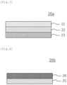
- FIG. 2 is a schematic sectional view of a light control element according to another embodiment of the present invention.
- a light control element 100b illustrated in FIG. 2 is a light control element of a gasochromic mode, and includes a glass film 10, a light control layer 20, a resin film 30, and a pressure-sensitive adhesive layer 40 in the stated order.
- the light control element 100b through intermediation of a spacer 60 between the glass film 10 and the light control layer 20, the light control element 100b has a void 70 configured to introduce a gas.
- the spacer 60 may be omitted as long as the void configured to introduce a gas is ensured.
- the light control layer 20 contains a gasochromic material.
- the light control element of the present invention may be a light control element of a mode different from those of the illustrated examples (e.g., a thermochromic mode or a photochromic mode).
- a release film may be laminated on a side of the pressure-sensitive adhesive layer on which the resin film is not arranged.
- the thickness of the light control element is, for example, from 70 um to 500 um, preferably from 80 um to 450 um, more preferably from 100 um to 400 um, still more preferably from 140 um to 400 um.
- the bending radius of the light control element is from 20 mm to 80 mm.
- the light control element has a bending radius falling within the above-mentioned ranges, the light control element is excellent in flexibility, and hence can be taken up into a roll shape to form a film roll.
- handleability at the time of bonding the light control element to a glass surface or the like is satisfactory.
- any appropriate glass film may be adopted as the glass film.
- glass for forming the glass film according to classification based on a composition, there are given, for example, soda lime glass, borate glass, aluminosilicate glass, and quartz glass.
- soda lime glass for example, soda lime glass, borate glass, aluminosilicate glass, and quartz glass.
- alkali component there are given alkali-free glass and low-alkali glass.
- the content of an alkali metal component (e.g., Na 2 O, K 2 O, or Li 2 O) in the glass is preferably 15 wt% or less, more preferably 10 wt% or less.
- the total light transmittance of the glass film is, for example, 80% or more, preferably 85% or more, more preferably 90% or more.
- the thickness of the glass film is from 50 um to 180 um. When the thickness of the glass film is less than 50 um, the impact resistance becomes insufficient in some cases. Meanwhile, when the thickness of the glass film is more than 200 ⁇ m, the flexibility of the light control element is reduced, and the weight thereof is increased, and hence handleability at the time of bonding the light control element to a glass surface or the like may be reduced.
- a material for forming the resin film is typically a thermoplastic resin.
- the thermoplastic resin include: a polyester-based resin, such as PET; a cycloolefin-based resin, such as polynorbornene; an acrylic resin; a polycarbonate resin; and a cellulose-based resin. Of those, a polyester-based resin, a cycloolefin-based resin, or an acrylic resin is preferred. Those resins are each excellent in, for example, transparency, mechanical strength, thermal stability, and water barrier property. Those thermoplastic resins may be used alone or in combination thereof.
- an optical film to be used in a polarizing plate for example, a low-retardation base material, a high-retardation base material, a retardation plate, or a brightness enhancement film may also be used.
- the modulus of elasticity (tensile modulus of elasticity) at 23°C of the resin film may be preferably from 2 GPa to 10 GPa, more preferably from 2 GPa to 6 GPa.
- a glass material having high brittleness is suitably supported, and as a result, a light control element excellent in flexibility can be obtained.
- the thickness of the resin film is from 30 um to 150 um.
- the glass material having high brittleness can be suitably supported, and the thickness of the light control element can be reduced. As a result, a light control element excellent in flexibility can be obtained.
- the total light transmittance of the resin film is preferably 60% or more, more preferably 70% or more, still more preferably 80% or more.
- a light control layer containing a liquid crystal compound is typically formed by dispersing a liquid crystal compound in a polymer matrix.
- a light transmitting state and a light scattering state can be switched by changing the degree of alignment of the liquid crystal compound based on the presence or absence of the application of a voltage.
- the light control layer is in the light transmitting state at the time of application of a voltage, and the light control layer is in the light scattering state at the time of application of no voltage (normal mode).
- the liquid crystal compound is not aligned at the time of application of no voltage, resulting in the light scattering state.
- the liquid crystal compound is aligned, and the refractive index of the liquid crystal compound and the refractive index of the polymer matrix match with each other, resulting in the light transmitting state.
- the light control layer is in the light scattering state at the time of application of a voltage, and the light control layer is in the light transmitting state at the time of application of no voltage (reverse mode).
- the liquid crystal compound is aligned at the time of application of no voltage, resulting in the light transmitting state.
- the alignment of the liquid crystal compound is disturbed, resulting in the light scattering state.
- Examples of the light control layer as described above include a light control layer containing a polymer-dispersed liquid crystal and a light control layer containing a polymer-network liquid crystal.
- the polymer-dispersed liquid crystal has a structure in which a liquid crystal compound in the form of droplets is dispersed in a polymer matrix.
- the polymer-network liquid crystal has a structure in which a liquid crystal compound is dispersed in a polymer network.
- the liquid crystal has a continuous phase in the polymer network.
- liquid crystal compound of a non-polymeric type is used as the liquid crystal compound.
- the liquid crystal compound may have positive dielectric anisotropy or negative dielectric anisotropy.
- the liquid crystal compound may include nematic, smectic, and cholesteric liquid crystal compounds.
- a nematic liquid crystal compound is preferably used because excellent transparency can be achieved under the light transmitting state.
- nematic liquid crystal compound examples include a biphenyl-based compound, a phenyl benzoate-based compound, a cyclohexylbenzene-based compound, an azoxybenzene-based compound, an azobenzene-based compound, an azomethine-based compound, a terphenyl-based compound, a biphenyl benzoate-based compound, a cyclohexylbiphenyl-based compound, a phenylpyridine-based compound, a cyclohexylpyrimidine-based compound, a cholesterol-based compound, and a fluorine-based compound.
- the content of the liquid crystal compound in the light control layer is, for example, 40 wt% or more, preferably from 50 wt% to 99 wt%, more preferably from 50 wt% to 95 wt%.
- a resin for forming the polymer matrix may be appropriately selected depending on, for example, the light transmittance and the refractive index of the liquid crystal compound.
- the resin may be an optically isotropic resin or may be an optically anisotropic resin.
- the resin is an active energy ray-curable resin.
- a liquid crystal polymer obtained by curing a polymerizable liquid crystal compound, a (meth) acrylic resin, a silicone-based resin, an epoxy-based resin, a fluorine-based resin, a polyester-based resin, and a polyimide resin may be preferably used.
- the content of the polymer matrix in the light control layer is preferably from 1 wt% to 60 wt%, more preferably from 5 wt% to 50 wt%.
- the content of the polymer matrix is less than 1 wt%, a problem of, for example, a reduction in adhesiveness with a transparent electrode layer may occur.
- the content of the polymer matrix is more than 60 wt%, a problem of, for example, an increase in driving voltage or a reduction in light control function may occur.
- the thickness of the light control layer may be, for example, from 10 um to 100 um, preferably from 15 um to 60 um.
- FIG. 3 is a schematic sectional view of an example of a light control layer containing an electrochromic material which can be used in the present invention.
- a light control layer 20a containing an electrochromic material includes a first electrochromic compound layer 21 (first EC layer), an electrolyte layer 22, and a second electrochromic compound layer 23 (second EC layer) in the stated order.
- the thickness of the light control layer 20a is, for example, from 0.1 um to 400 um, preferably from 0.5 ⁇ m to 200 um.
- the first EC layer along with the second EC layer described later, is a light control layer configured to change its light transmittance or color in accordance with an electric current flowing in the first EC layer.
- An electrochromic compound for forming the first EC layer is not limited, and examples thereof include: inorganic electrochromic compounds, such as tungsten oxide (e.g., WO 3 ), molybdenum oxide, vanadium oxide, indium oxide, iridium oxide, nickel oxide, and Prussian blue; and organic electrochromic compounds, such as a phthalocyanine-based compound, a styryl-based compound, a viologen-based compound, polypyrrole, polyaniline, and polythiophene (e.g., poly(ethylene dioxythiophene)-poly(styrenesulfonate)).
- Preferred examples thereof include tungsten oxide and polythiophene.
- the thickness of the first EC layer 21 is, for example, 0.01 ⁇ m or more, preferably 0.05 um or more, and is, for example, 40 um or less, preferably 20 um or less.
- the electrolyte layer is a layer configured to efficiently achieve electrical conduction to the electrochromic compounds in the first EC layer and the second EC layer.
- the electrolyte layer may be formed of a liquid electrolyte and a sealing material for sealing the liquid electrolyte, or may be formed of a solid electrolyte film.
- the electrolyte for forming the electrolyte layer is not limited, and examples thereof include alkali metal salts and alkaline earth metal salts, such as LiClO 4 , LiBF 4 , LiAsF 6 , LiPF 6 , LiCF 3 SO 3 , LiCF 3 COO, KCl, NaClO 3 , NaCl, NaBF 4 , NaSCN, KBF 4 , Mg(ClO 4 ) 2 , and Mg(BF 4 ) 2 .
- the examples also include quaternary ammonium salts and quaternary phosphonium salts.
- an organic solvent is preferably used in combination with the electrolyte.
- the organic solvent is not limited as long as the electrolyte can be dissolved therein, and examples thereof include: carbonates, such as ethylene carbonate, propylene carbonate, and methyl carbonate; furans, such as tetrahydrofuran; and ⁇ -butyrolactone, 1,2-dimethoxyethane, 1,3-dioxolane, 4-methyl-1,3-dioxolane, methyl formate, methyl acetate, methyl propionate, acetonitrile, propylene carbonate, and N,N-dimethylformamide.
- a preferred example of the electrolyte layer is an electrolyte film including the electrolyte, the organic solvent, and a binder resin.
- Such electrolyte layer is obtained, for example, by mixing: an electrolyte solution in which the electrolyte is dissolved in the organic solvent; and the binder resin, followed by drying.
- binder resin is an acrylic resin, such as polymethyl methacrylate.
- the thickness of the electrolyte layer is, for example, 0.01 um or more, preferably 0.1 um or more, and is, for example, 300 um or less, preferably 100 um or less.
- the same description as that of the first EC layer can be applied to the second EC layer.
- the second EC layer may have the same configuration as or a different configuration from that of the first EC layer.
- FIG. 4 is a schematic sectional view of an example of a light control layer containing a gasochromic material which can be used in the present invention.
- a light control layer 20b containing a gasochromic material includes a gasochromic compound layer 25 (GC layer) and a catalyst layer 26.
- the light control layer 20b containing a gasochromic material is typically arranged so that the catalyst layer 26 is brought into contact with a gas (on a void side) .
- the GC layer contains a chromic material which is reversibly changed in state between a transparent state caused by hydrogenation and a reflection state caused by dehydrogenation.
- the chromic material for forming the GC layer include: rare earth metals, such as Y, La, Gd, and Sm; alloys of rare earth metals and magnesium; alloys of alkaline earth metals, such as Ca, Sr, and Ba, and magnesium; and alloys of transition metals, such as Ni, Mn, Co, and Fe, and magnesium.
- the GC layer preferably contains magnesium because such GC layer is excellent in transparency when hydrogenated. Alloys of rare earth metal elements and magnesium are more preferred from the viewpoint of achieving both transparency and durability.
- the GC layer may contain an element other than the alloy as a trace component.
- the above-mentioned metal or alloy for forming the GC layer includes a metal element which becomes a transparent state when hydrogenated, and which becomes a reflection state when releasing hydrogen.
- a metal element which becomes a transparent state when hydrogenated, and which becomes a reflection state when releasing hydrogen.
- the thickness of the GC layer is not particularly limited, but from the viewpoint of achieving both a light transmittance in the transparent state and a light shielding rate (reflectance) in the reflection state, is preferably from 10 nm to 500 nm, more preferably from 15 nm to 200 nm, still more preferably from 20 nm to 100 nm.
- the thickness of the GC layer is excessively small, the light reflectance in the reflection state tends to be reduced.
- the thickness of the GC layer is excessively large, the light transmittance in the transparent state tends to be reduced.
- the catalyst layer has a function of promoting the hydrogenation and dehydrogenation of the GC layer.
- the switching rates of switching from the reflection state to the transparent state (hydrogenation of the GC layer) and switching from the transparent state to the reflection state (dehydrogenation of the GC layer) are increased.
- a material for forming the catalyst layer is not particularly limited as long as the material has a function of promoting the hydrogenation and dehydrogenation of the GC layer, but preferably includes, for example, at least one kind of metal selected from palladium, platinum, a palladium alloy, and a platinum alloy.
- palladium is suitably used because of having high hydrogen permeability.
- the thickness of the catalyst layer may be appropriately set depending on, for example, the reactivity of the GC layer and the catalytic ability of the catalyst layer.
- the thickness of the catalyst layer is, for example, from 1 nm to 30 nm, preferably from 2 nm to 20 nm.
- the thickness of the catalyst layer is excessively small, the catalytic function on the hydrogenation and dehydrogenation is not sufficiently exhibited in some cases.
- the thickness of the catalyst layer is excessively large, the light transmittance tends to be reduced.
- the GC layer and the catalyst layer may be sequentially formed on the resin film by a sputtering method.
- the light control layer 20b containing a gasochromic material may further include a layer other than the GC layer 25 and the catalyst layer 26 as required.
- a base layer may be arranged on a side of the GC layer on which the catalyst layer is not arranged (e.g., between the resin film and the GC layer), or a buffer layer may be arranged between the GC layer and the catalyst layer.
- a surface layer may be arranged on the catalyst layer.
- an inorganic oxide layer is formed as the base layer between the resin film and the GC layer, water, an oxygen gas, or the like generated from the resin film is blocked, and the oxidation of the GC layer can be suppressed.
- a metal thin film formed of, for example, Ti, Nb, V, or an alloy of any of these metals is arranged as the buffer layer between the GC layer and the catalyst layer, while the migration of magnesium or the like from the GC layer to the catalyst layer is suppressed, the switching rate of switching from the transparent state to the reflection state caused by the dehydrogenation tends to be increased.
- the surface layer may have a function of blocking the permeation of water or oxygen to prevent the oxidation of the GC layer.
- an inorganic material such as an inorganic oxide
- an organic material such as a polymer
- an organic-inorganic hybrid material for example, an organic-inorganic hybrid material.
- the transparent electrode layers may be each formed of, for example, a metal oxide, such as indium tin oxide (ITO), zinc oxide (ZnO), or tin oxide (SnO 2 ).
- the transparent electrode layer may be formed of a metal nanowire such as a silver nanowire (AgNW), a carbon nanotube (CNT), an organic conductive film, a metal layer, or a laminate thereof .
- the transparent electrode layer may be patterned into a desired shape depending on the purposes .
- the total light transmittance of the transparent electrode layer is preferably 80% or more, more preferably 85% or more, still more preferably 90% or more.
- the surface resistance value of the transparent electrode layer is preferably from 0.1 ⁇ / ⁇ to 1,000 ⁇ / ⁇ , more preferably from 0.5 ⁇ / ⁇ to 500 ⁇ / ⁇ , still more preferably from 1 ⁇ / ⁇ to 250 ⁇ / ⁇ .
- the thickness of the transparent electrode layer is preferably from 0.01 um to 0.06 um, more preferably from 0.01 um to 0.045 um. When the thickness of the transparent electrode layer falls within the above-mentioned ranges, an electrode layer excellent in conductivity and light transmitting property can be obtained.
- the transparent electrode layer may be formed on the glass film or the resin film by a method such as sputtering.
- the transparent electrode layer may be directly formed on those films, or as required, may be formed through intermediation of, for example, a refractive index adjusting layer or a support base material.
- any appropriate pressure-sensitive adhesive composition may be used as a pressure-sensitive adhesive composition for forming the pressure-sensitive adhesive layer.
- the usable pressure-sensitive adhesive composition include pressure-sensitive adhesive compositions containing, as base polymers, a (meth)acrylic polymer, a silicone-based polymer, polyester, polyurethane, polyamide, polyether, a fluorine-based polymer, a rubber-based polymer, and the like.
- an acrylic pressure-sensitive adhesive composition containing an acrylic polymer as a base polymer is preferred.
- the pressure-sensitive adhesive composition may further contain any appropriate additive as required.
- the additive include a cross-linking agent, a tackifier, a plasticizer, a pigment, a dye, a filler, an age resistor, a conductive material, a UV absorber, a light stabilizer, a release modifier, a softener, a surfactant, a flame retardant, and an antioxidant.
- cross-linking agent examples include an isocyanate-based cross-linking agent, an epoxy-based cross-linking agent, a peroxide-based cross-linking agent, a melamine-based cross-linking agent, a urea-based cross-linking agent, a metal alkoxide-based cross-linking agent, a metal chelate-based cross-linking agent, a metal salt-based cross-linking agent, a carbodiimide-based cross-linking agent, an oxazoline-based cross-linking agent, an aziridine-based cross-linking agent, and an amine-based cross-linking agent.
- the modulus of elasticity at 23°C (storage modulus of elasticity) of the pressure-sensitive adhesive layer may be preferably from 1 ⁇ 10 -5 GPa to 1 ⁇ 10 -2 GPa, more preferably from 5.0 ⁇ 10 -5 GPa to 5.0 ⁇ 10 -3 GPa, still more preferably from 1.0 ⁇ 10 -4 GPa to 1.0 ⁇ 10 -3 GPa.
- the pressure-sensitive adhesive layer having such modulus of elasticity may contribute to improvements in impact resistance and handleability at the time of bonding.
- the pressure-sensitive adhesive layer having such modulus of elasticity may function as an impact relaxation layer in the case where the light control element having an elongated shape is taken up into a roll shape.
- the thickness (dry thickness) of the pressure-sensitive adhesive layer is determined depending on desired adhesion (peel strength).
- the thickness (dry thickness) of the pressure-sensitive adhesive layer may be set to preferably from about 20 um to about 200 um, more preferably from 20 um to 150 um, still more preferably from 25 um to 100 um.
- the above-mentioned light control element may be produced by any appropriate method.
- a case of producing the light control element including the light control layer containing a liquid crystal compound by a roll-to-roll process is illustratively described below.
- a light control film may be obtained, for example, by a method involving: unwinding, from a roll, an elongated resin film with a transparent electrode layer in which the transparent electrode layer has been formed on one surface in advance; while conveying the resin film with a transparent electrode layer in a lengthwise direction, applying a composition for forming a light control layer on the surface of the transparent electrode layer to form an application layer; continuously laminating, on the application layer, an elongated glass film with a transparent electrode layer in which the transparent electrode layer has been formed on one surface in advance so that the transparent electrode layer of the glass film faces the application layer and the elongated directions of the resin film and the glass film match with each other, to thereby form a laminate; curing the application layer to obtain a light control film; continuously la
- a glass film roll with a light control layer includes a glass film having an elongated shape having a thickness of from 50 um to 200 um, and a light control layer laminated on one side of the glass film.
- the glass film roll with a light control layer includes a glass film, a light control layer, a resin film, and a pressure-sensitive adhesive layer in the stated order.
- the glass film, the light control layer, the resin film, and the pressure-sensitive adhesive layer the ones described in the section A are used.
- the glass film roll with a light control layer is the light control element described in the section A which has been formed into an elongated shape and taken up into a roll shape.
- the glass film roll with a light control layer has a light weight and high reliability (e.g., impact resistance and scratch resistance), and when a pressure-sensitive adhesive layer is incorporated therein, the glass film roll with a light control layer can easily be bonded to a glass surface or the like.
- a strip-shaped sample having a thickness of 50 um, a width of 2 cm, and a length of 15 cm was produced, and its modulus of elasticity was measured with an autograph (manufactured by Shimadzu Corporation, AG-I) from the elongation of the strip-shaped sample in its lengthwise direction and a stress.
- the test conditions were as follows: a chuck-to-chuck distance was set to 10 cm, and a tensile rate was set to 10 mm/min.
- the storage modulus of elasticity at 23°C of a pressure-sensitive adhesive layer was measured with a viscoelasticity-measuring apparatus ARES (manufactured by TA Instruments, Inc.). Specifically, the pressure-sensitive adhesive layer was formed into a sheet shape having a thickness of 2 mm, and the sheet was punched into a shape in accordance with parallel plates each having a diameter of 25 mm, followed by its mounting between the chucks of the apparatus. Then, under a condition in which the temperature of the layer was increased from -70°C to 150°C at a temperature increase rate of 5°C/min while strain was applied thereto at a frequency of 1 Hz, its storage modulus of elasticity at 23°C was measured.
- ARES viscoelasticity-measuring apparatus
- a thickness was measured with a dial gauge.
- an acrylic pressure-sensitive adhesive composition A 100 Parts by weight of the solid content of the acrylic polymer solution was uniformly mixed with 0.5 part by weight of a trimethylolpropane-tolylene diisocyanate adduct (manufactured by Nippon Polyurethane Industry Co., Ltd., CORONATE L) serving as an isocyanate-based cross-linking agent and 0.1 part by weight of a silane coupling agent (manufactured by Shin-Etsu Chemical Co., Ltd., KBM-403), followed by stirring.
- a trimethylolpropane-tolylene diisocyanate adduct manufactured by Nippon Polyurethane Industry Co., Ltd., CORONATE L
- silane coupling agent manufactured by Shin-Etsu Chemical Co., Ltd., KBM-403
- a transparent electrode layer (ITO layer) was formed on one surface of a transparent PET base material (manufactured by Mitsubishi Chemical Corporation, "DIAFOIL", thickness: 188 um, modulus of elasticity: 4.0 GPa) by sputtering. Thus, a PET film with an electrode layer was obtained.
- a transparent PET base material manufactured by Mitsubishi Chemical Corporation, "DIAFOIL”, thickness: 188 um, modulus of elasticity: 4.0 GPa
- a transparent electrode layer (ITO layer) was formed on one surface of a glass film (manufactured by Nippon Electric Glass Co., Ltd., "OA-10G", thickness: 150 um) by sputtering. Thus, a glass film with an electrode layer was obtained.
- the pressure-sensitive adhesive composition A was applied onto the release treatment surface, followed by drying.
- a release film with a pressure-sensitive adhesive layer was obtained.
- the pressure-sensitive adhesive layer had a thickness of 50 um and a modulus of elasticity of 4 ⁇ 10 -4 GPa.
- the PET film with an electrode layer and the glass film with an electrode layer were bonded to each other through intermediation of a composition for forming a light control layer (polymer-dispersed liquid crystal layer), which contained nematic liquid crystal molecules and 1,6-hexanediol diacrylate (manufactured by Nippon Kayaku Co., Ltd., "HDDA"), so that the ITO layers faced each other.
- a composition for forming a polymer-dispersed liquid crystal layer was cured. Thus, a laminate was obtained.
- the release film with a pressure-sensitive adhesive layer was laminated on the laminate so that the pressure-sensitive adhesive layer faced the PET film.
- a light control element having a configuration of [glass film/transparent electrode layer/light control layer/transparent electrode layer/resin film/pressure-sensitive adhesive layer/release film] was obtained.
- the thickness of the light control element from the glass film to the pressure-sensitive adhesive layer was 408 um.
- a light control element having a configuration of [glass film/transparent electrode layer/light control layer/transparent electrode layer/resin film/pressure-sensitive adhesive layer/release film] was obtained in the same manner as in Example 1 except that a transparent PET base material (manufactured by Mitsubishi Chemical Corporation, "DIAFOIL", thickness: 50 um, modulus of elasticity: 4.0 GPa) was used as the resin film, and a glass film (manufactured by Nippon Electric Glass Co., Ltd., "OA-10G", thickness: 100 um) was used as the glass film.
- the thickness of the light control element from the glass film to the pressure-sensitive adhesive layer was 220 um.
- a light control element having a configuration of [glass film/transparent electrode layer/light control layer/transparent electrode layer/resin film/pressure-sensitive adhesive layer/release film] was obtained in the same manner as in Example 1 except that a transparent PET base material (manufactured by Mitsubishi Chemical Corporation, "DIAFOIL”, thickness: 50 um, modulus of elasticity: 4.0 GPa) was used as the resin film, a glass film (manufactured by Nippon Electric Glass Co., Ltd., "OA-10G", thickness: 70 um) was used as the glass film, and the thickness of the pressure-sensitive adhesive layer was changed to 20 um. The thickness of the light control element from the glass film to the pressure-sensitive adhesive layer was 160 um.
- a light control element having a configuration of [glass film/transparent electrode layer/light control layer/transparent electrode layer/resin film/pressure-sensitive adhesive layer/release film] was obtained in the same manner as in Example 1 except that a glass film (manufactured by Nippon Electric Glass Co., Ltd., "OA-10G", thickness: 300 um) was used as the glass film.
- the thickness of the light control element from the glass film to the pressure-sensitive adhesive layer was 558 um.
- a light control element having a configuration of [first resin film/transparent electrode layer/light control layer/transparent electrode layer/second resin film/pressure-sensitive adhesive layer/release film] was obtained in the same manner as in Example 1 except that a transparent PET base material (manufactured by Mitsubishi Chemical Corporation, "DIAFOIL”, thickness: 50 um, modulus of elasticity: 4.0 GPa) was used as the resin film, a transparent PET base material (manufactured by Mitsubishi Chemical Corporation, "DIAFOIL”, thickness: 100 um) was used instead of the glass film, and the thickness of the pressure-sensitive adhesive layer was changed to 20 ⁇ m. The thickness of the light control element from the first resin film to the pressure-sensitive adhesive layer was 190 um.
- a light control element having a configuration of [glass film/transparent electrode layer/light control layer/transparent electrode layer/resin film/pressure-sensitive adhesive layer/release film] was obtained in the same manner as in Example 1 except that a transparent PET base material (manufactured by Mitsubishi Chemical Corporation, "DIAFOIL", thickness: 300 um, modulus of elasticity: 4.0 GPa) was used as the resin film, and a glass film (manufactured by Nippon Electric Glass Co., Ltd., "OA-10G", thickness: 100 um) was used as the glass film.
- the thickness of the light control element from the glass film to the pressure-sensitive adhesive layer was 470 um.
- a light control element having a configuration of [glass film/transparent electrode layer/light control layer/transparent electrode layer/resin film/pressure-sensitive adhesive layer/release film] was obtained in the same manner as in Example 1 except that a transparent PET base material (manufactured by Mitsubishi Chemical Corporation, "DIAFOIL”, thickness: 50 um, modulus of elasticity: 4.0 GPa) was used as the resin film, a glass film (manufactured by Nippon Electric Glass Co., Ltd., "OA-10G", thickness: 35 um) was used as the glass film, and the thickness of the pressure-sensitive adhesive layer was changed to 20 um. The thickness of the light control element from the glass film to the pressure-sensitive adhesive layer was 125 um.
- a plurality of poles made of vinyl chloride having different radii were prepared so that their radii were ranged from 20 mm to 100 mm in increments of 10 mm.
- a sample of the light control element from which the release film had been peeled off was bent along any one of the poles so that its glass film side (in Comparative Example 2, its first resin film side) faced outward, the degree of bending of the sample was confirmed as to whether both sides thereof were able to be fixed with CELLOTAPE (manufactured by Nichiban Co., Ltd, "CT405AP-24", pressure-sensitive adhesive strength: 3.93 N/10 cm) or could not be fixed with CELLOTAPE, or the sample broke, and the minimum radius of the poles to which both the sides were able to be fixed without breakage was regarded as the bending radius thereof.
- the size of the sample was as follows: the length of its short side was set to 20 mm, and the length of its long side was set to the radius of the outer diameter of each pole.
- the light control element having a size of 5 cm by 5 cm from which the release film had been peeled off was bonded to a glass sheet to provide an evaluation sample.
- a puncture rod ( ⁇ 0.5 mm) was dropped onto the sample from a height of 10 cm at a rate of 20 mm/min, and the breakage of the glass film was observed.
- the impact resistance was evaluated based on the following criteria.
- Steel wool #1000 was uniformly attached to a smooth sectional surface of a cylinder having a diameter of 25 mm.
- a sample of the light control element was arranged thereon so that its surface on a glass film side (in Comparative Example 2, its surface on a first resin film side) was brought into contact with the steel wool, and was reciprocated 30 times at a rate of about 100 mm/sec at a load of 1.5 kg. After that, the scratch resistance was judged by visual evaluation based on the following criteria.
- each of the light control elements of Examples is satisfactory in each of impact resistance and scratch resistance, and thus has high reliability.
- the light control element when the light control element is bonded to a window or the like, its glass surface serves as an exposure surface, and hence the light control element may be excellent in durability.
- the light control element had a light weight and appropriate flexibility, and hence was excellent in handleability at the time of bonding.
- each of the light control elements of Comparative Examples was insufficient in any of impact resistance and scratch resistance, or was insufficient in flexibility, resulting in a problem in handleability at the time of bonding.
- the present invention is suitably used in the field of a light control film.
Landscapes
- Physics & Mathematics (AREA)
- Nonlinear Science (AREA)
- General Physics & Mathematics (AREA)
- Optics & Photonics (AREA)
- Chemical & Material Sciences (AREA)
- Mathematical Physics (AREA)
- Crystallography & Structural Chemistry (AREA)
- Organic Chemistry (AREA)
- Laminated Bodies (AREA)
- Liquid Crystal (AREA)
- Electrochromic Elements, Electrophoresis, Or Variable Reflection Or Absorption Elements (AREA)
- Window Of Vehicle (AREA)
- Surface Treatment Of Glass (AREA)
- Glass Compositions (AREA)
- Electroluminescent Light Sources (AREA)
Claims (5)
- Lichtsteuerungselement (100), umfassend einen Glasfilm (10), eine Lichtsteuerungsschicht (20), einen Harzfilm (30) und eine druckempfindliche Klebeschicht (40) in der angegebenen Reihenfolge, wobei die Lichtsteuerungsschicht zwischen dem Glasfilm und dem Harzfilm, die als Basismaterialien dienen, eingebettet ist,wobei das Lichtsteuerungselement einen Biegeradius von 20 mm bis 80 mm aufweist,wobei der Glasfilm eine Dicke von 50 µm bis 180 µm aufweist, wobeider Harzfilm eine Dicke von 30 µm bis 150 µm aufweist.
- Lichtsteuerungselement nach Anspruch 1,
wobei der Harzfilm einen Elastizitätsmodul bei 23 °C von 2 GPa bis 10 GPa aufweist. - Lichtsteuerungselement nach Anspruch 1 oder 2,wobei die druckempfindliche Klebeschicht eine Dicke von 20 µm bis 200 µm aufweist, undwobei die druckempfindliche Klebeschicht einen Elastizitätsmodul bei 23 °C von 1×10⁻⁵ GPa bis 1×10⁻² GPa aufweist.
- Lichtsteuerungselement nach einem der Ansprüche 1 bis 3, wobei eine Dicke des Lichtsteuerungselements von dem Glasfilm bis zur druckempfindlichen Klebeschicht 70 µm bis 500 µm ist.
- Glasfilmrolle, die das Lichtsteuerungselement nach einem der Ansprüche 1 bis 4 ist, die in eine längliche Form ausgebildet und in eine Rollenform aufgenommen ist.
Applications Claiming Priority (2)
| Application Number | Priority Date | Filing Date | Title |
|---|---|---|---|
| JP2018061556 | 2018-03-28 | ||
| PCT/JP2019/011955 WO2019188736A1 (ja) | 2018-03-28 | 2019-03-22 | ガラスフィルムを含む調光素子 |
Publications (3)
| Publication Number | Publication Date |
|---|---|
| EP3779577A1 EP3779577A1 (de) | 2021-02-17 |
| EP3779577A4 EP3779577A4 (de) | 2021-11-24 |
| EP3779577B1 true EP3779577B1 (de) | 2024-10-23 |
Family
ID=68060032
Family Applications (1)
| Application Number | Title | Priority Date | Filing Date |
|---|---|---|---|
| EP19775974.9A Active EP3779577B1 (de) | 2018-03-28 | 2019-03-22 | Dimmelement mit glasfilm |
Country Status (7)
| Country | Link |
|---|---|
| US (1) | US11143892B2 (de) |
| EP (1) | EP3779577B1 (de) |
| JP (1) | JP7274458B2 (de) |
| KR (1) | KR102865558B1 (de) |
| CN (1) | CN111902769B (de) |
| TW (1) | TWI822743B (de) |
| WO (1) | WO2019188736A1 (de) |
Families Citing this family (4)
| Publication number | Priority date | Publication date | Assignee | Title |
|---|---|---|---|---|
| US20220075218A1 (en) * | 2018-12-17 | 2022-03-10 | Nitto Denko Corporation | Light control film |
| JP7596897B2 (ja) | 2021-03-31 | 2024-12-10 | 株式会社リコー | エレクトロクロミック素子 |
| US20250155743A1 (en) * | 2022-02-16 | 2025-05-15 | Agp Worldwide Operations Gmbh | Variable light transmission glazing with high complexity curvature |
| CN114942553B (zh) * | 2022-05-18 | 2023-11-14 | 京东方科技集团股份有限公司 | 显示基板及其控制方法和显示装置 |
Citations (1)
| Publication number | Priority date | Publication date | Assignee | Title |
|---|---|---|---|---|
| CN106082711A (zh) * | 2016-06-02 | 2016-11-09 | 中国科学院广州能源研究所 | 一种智能调光节能夹层玻璃及其制备方法 |
Family Cites Families (33)
| Publication number | Priority date | Publication date | Assignee | Title |
|---|---|---|---|---|
| US4268134A (en) * | 1979-03-07 | 1981-05-19 | Corning Glass Works | Lightweight laminated photochromic lenses |
| JPH04130311A (ja) * | 1990-09-21 | 1992-05-01 | Dainippon Ink & Chem Inc | 液晶デバイス及びその製造方法 |
| JPH08201780A (ja) * | 1995-01-20 | 1996-08-09 | Alps Electric Co Ltd | 液晶表示媒体 |
| WO2002074532A1 (en) * | 2001-03-15 | 2002-09-26 | Mitsui Chemicals Inc. | Laminated body and display device using the laminated body |
| JP4060249B2 (ja) * | 2003-07-29 | 2008-03-12 | 日本板硝子株式会社 | 調光体及び合わせガラス |
| JP4378314B2 (ja) * | 2005-04-26 | 2009-12-02 | シャープ株式会社 | 表示装置及び表示装置の製造方法 |
| JP5233676B2 (ja) | 2006-12-21 | 2013-07-10 | 日立化成株式会社 | 調光フィルム及び調光ガラス |
| JP4228026B2 (ja) * | 2007-02-28 | 2009-02-25 | 日東電工株式会社 | バックライトシステムおよび粘着剤付光学シート |
| JP2010208861A (ja) | 2007-07-03 | 2010-09-24 | Asahi Glass Co Ltd | 調光窓材 |
| JP2009169229A (ja) * | 2008-01-18 | 2009-07-30 | Mitsui Chemicals Inc | エレクトロクロミック素子およびその製造方法 |
| JP2009242633A (ja) * | 2008-03-31 | 2009-10-22 | Lintec Corp | 光学用粘着剤シート、粘着剤付き光学部材及びその製造方法 |
| TWI475282B (zh) * | 2008-07-10 | 2015-03-01 | Semiconductor Energy Lab | 液晶顯示裝置和其製造方法 |
| CN102385187B (zh) | 2010-09-06 | 2013-12-11 | 北京众智同辉科技有限公司 | 一种复合式电致液晶雾化玻璃及其制作方法 |
| JP2012186315A (ja) * | 2011-03-04 | 2012-09-27 | Nitto Denko Corp | 薄膜基板の製造方法 |
| JP2013148687A (ja) * | 2012-01-19 | 2013-08-01 | Konica Minolta Inc | 調光フィルム、及び調光フィルムの製造方法 |
| US20140132883A1 (en) * | 2012-11-13 | 2014-05-15 | 3M Innovative Properties Company | Optical stack including light extraction layer and polymer dispersed liquid crystal layer |
| US20140267983A1 (en) * | 2013-03-15 | 2014-09-18 | Yi-Ta Chen | Switchable glass patch, switchable glass, and manufacturing method thereof |
| CN203299484U (zh) * | 2013-06-19 | 2013-11-20 | 珠海兴业光电科技有限公司 | 自粘式调光膜 |
| JP2015071284A (ja) | 2013-09-09 | 2015-04-16 | アキレス株式会社 | 調光自己粘着積層体 |
| US9321677B2 (en) * | 2014-01-29 | 2016-04-26 | Corning Incorporated | Bendable glass stack assemblies, articles and methods of making the same |
| CN105334658A (zh) | 2014-07-14 | 2016-02-17 | 法国圣戈班玻璃公司 | 调光玻璃结构以及车窗 |
| JP6900156B2 (ja) * | 2015-05-21 | 2021-07-07 | 日東電工株式会社 | 調光フィルムおよびその製造方法、ならびに調光素子 |
| WO2016186130A1 (ja) | 2015-05-21 | 2016-11-24 | 日東電工株式会社 | 調光フィルムおよびその製造方法、ならびに調光素子 |
| JP6757176B2 (ja) * | 2015-05-21 | 2020-09-16 | 日東電工株式会社 | 調光フィルムおよびその製造方法、ならびに調光素子 |
| JP2017003906A (ja) * | 2015-06-15 | 2017-01-05 | 日東電工株式会社 | 両面粘着剤層付偏光フィルムおよび画像表示装置 |
| JP6096847B2 (ja) | 2015-08-07 | 2017-03-15 | ▲き▼芯科技股▲ふん▼有限公司 | 高分子分散型液晶調光構成 |
| JP6412539B2 (ja) * | 2015-11-09 | 2018-10-24 | 日東電工株式会社 | 光透過性導電フィルムおよび調光フィルム |
| CN108367980A (zh) * | 2015-12-09 | 2018-08-03 | 旭硝子株式会社 | 夹层玻璃 |
| JP2017182062A (ja) | 2016-03-25 | 2017-10-05 | 日東電工株式会社 | 調光フィルムの製造方法 |
| US10288974B2 (en) * | 2016-04-06 | 2019-05-14 | Amazon Technologies, Inc. | Borderless display with curved edges |
| JP6142396B1 (ja) * | 2016-07-28 | 2017-06-07 | サイデン化学株式会社 | 光学フィルム粘着シート |
| WO2019026865A1 (ja) * | 2017-08-04 | 2019-02-07 | 日東電工株式会社 | 光取り出し部材 |
| CN107765490A (zh) * | 2017-11-27 | 2018-03-06 | 怡通科技有限公司 | 一种柔性电致变色隔热智能窗膜及其制备工艺 |
-
2019
- 2019-03-21 TW TW108109746A patent/TWI822743B/zh active
- 2019-03-22 JP JP2020509930A patent/JP7274458B2/ja active Active
- 2019-03-22 WO PCT/JP2019/011955 patent/WO2019188736A1/ja not_active Ceased
- 2019-03-22 CN CN201980021085.2A patent/CN111902769B/zh active Active
- 2019-03-22 KR KR1020207026079A patent/KR102865558B1/ko active Active
- 2019-03-22 US US16/979,633 patent/US11143892B2/en active Active
- 2019-03-22 EP EP19775974.9A patent/EP3779577B1/de active Active
Patent Citations (1)
| Publication number | Priority date | Publication date | Assignee | Title |
|---|---|---|---|---|
| CN106082711A (zh) * | 2016-06-02 | 2016-11-09 | 中国科学院广州能源研究所 | 一种智能调光节能夹层玻璃及其制备方法 |
Also Published As
| Publication number | Publication date |
|---|---|
| CN111902769B (zh) | 2024-07-02 |
| CN111902769A (zh) | 2020-11-06 |
| TWI822743B (zh) | 2023-11-21 |
| EP3779577A4 (de) | 2021-11-24 |
| JPWO2019188736A1 (ja) | 2021-04-08 |
| KR102865558B1 (ko) | 2025-09-26 |
| EP3779577A1 (de) | 2021-02-17 |
| JP7274458B2 (ja) | 2023-05-16 |
| KR20200136899A (ko) | 2020-12-08 |
| WO2019188736A1 (ja) | 2019-10-03 |
| TW201941946A (zh) | 2019-11-01 |
| US11143892B2 (en) | 2021-10-12 |
| US20210026183A1 (en) | 2021-01-28 |
Similar Documents
| Publication | Publication Date | Title |
|---|---|---|
| EP3779577B1 (de) | Dimmelement mit glasfilm | |
| EP3045968A1 (de) | Elektrochrome vorrichtung, elektrochromes element und verfahren zur herstellung des elektrochromen elements | |
| KR102397860B1 (ko) | 플렉서블 전기변색소자 | |
| JP7171181B2 (ja) | 調光フィルム | |
| US11835832B2 (en) | Flexible electrochromic device | |
| KR102499890B1 (ko) | 셀 분할 전기변색소자 및 이의 제조방법 | |
| EP4586003A1 (de) | Elektrochromes element, verfahren zur herstellung davon und fenstervorrichtung damit | |
| EP4553569A1 (de) | Elektrochrome vorrichtung, laminat dafür, verfahren zur herstellung davon und fenstervorrichtung damit | |
| KR102704986B1 (ko) | 전기 변색 소자, 이의 제조방법 및 이를 포함하는 윈도우 장치 | |
| KR102704987B1 (ko) | 전기 변색 소자 및 이를 포함하는 윈도우 장치 | |
| KR102671407B1 (ko) | 전기 변색 소자 및 이를 포함하는 윈도우 장치 | |
| KR102671405B1 (ko) | 전기 변색 소자 및 이를 포함하는 윈도우 장치 | |
| KR102737211B1 (ko) | 전기 변색 소자, 이에 사용되는 적층체, 이의 제조 방법 및 이를 포함하는 윈도우 장치 | |
| KR102702630B1 (ko) | 전기 변색 소자 및 이를 포함하는 윈도우 장치 | |
| JP7452746B1 (ja) | エレクトロクロミックシートおよびエレクトロクロミック装置 | |
| KR102776664B1 (ko) | 전기 변색 소자 및 이를 포함하는 윈도우 장치 | |
| JP7327621B1 (ja) | 封止材料、エレクトロクロミックシートおよびエレクトロクロミック装置 | |
| EP4592744A1 (de) | Elektrochrome vorrichtung, herstellungsverfahren dafür und fenstervorrichtung damit | |
| KR102682436B1 (ko) | 전기 변색 소자 및 이를 포함하는 윈도우 장치 | |
| KR20240040866A (ko) | 전기 변색 소자의 제조방법 및 이에 사용되는 적층체 | |
| JP2026022982A (ja) | 電極、デバイス及び電極の製造方法 | |
| KR20240022260A (ko) | 전기 변색 소자 및 이를 포함하는 윈도우 장치 | |
| KR20240020434A (ko) | 전기 변색 소자 |
Legal Events
| Date | Code | Title | Description |
|---|---|---|---|
| STAA | Information on the status of an ep patent application or granted ep patent |
Free format text: STATUS: THE INTERNATIONAL PUBLICATION HAS BEEN MADE |
|
| PUAI | Public reference made under article 153(3) epc to a published international application that has entered the european phase |
Free format text: ORIGINAL CODE: 0009012 |
|
| STAA | Information on the status of an ep patent application or granted ep patent |
Free format text: STATUS: REQUEST FOR EXAMINATION WAS MADE |
|
| 17P | Request for examination filed |
Effective date: 20200924 |
|
| AK | Designated contracting states |
Kind code of ref document: A1 Designated state(s): AL AT BE BG CH CY CZ DE DK EE ES FI FR GB GR HR HU IE IS IT LI LT LU LV MC MK MT NL NO PL PT RO RS SE SI SK SM TR |
|
| AX | Request for extension of the european patent |
Extension state: BA ME |
|
| DAV | Request for validation of the european patent (deleted) | ||
| DAX | Request for extension of the european patent (deleted) | ||
| REG | Reference to a national code |
Ref country code: DE Ref legal event code: R079 Free format text: PREVIOUS MAIN CLASS: G02F0001130000 Ipc: G02F0001133300 Ref country code: DE Ref legal event code: R079 Ref document number: 602019060826 Country of ref document: DE Free format text: PREVIOUS MAIN CLASS: G02F0001130000 Ipc: G02F0001133300 |
|
| A4 | Supplementary search report drawn up and despatched |
Effective date: 20211027 |
|
| RIC1 | Information provided on ipc code assigned before grant |
Ipc: G02F 1/153 20060101ALI20211020BHEP Ipc: G02F 1/1333 20060101AFI20211020BHEP |
|
| STAA | Information on the status of an ep patent application or granted ep patent |
Free format text: STATUS: EXAMINATION IS IN PROGRESS |
|
| 17Q | First examination report despatched |
Effective date: 20230502 |
|
| GRAP | Despatch of communication of intention to grant a patent |
Free format text: ORIGINAL CODE: EPIDOSNIGR1 |
|
| STAA | Information on the status of an ep patent application or granted ep patent |
Free format text: STATUS: GRANT OF PATENT IS INTENDED |
|
| INTG | Intention to grant announced |
Effective date: 20240611 |
|
| RIN1 | Information on inventor provided before grant (corrected) |
Inventor name: WATANABE, KENTA Inventor name: SUGINO, AKIKO |
|
| GRAS | Grant fee paid |
Free format text: ORIGINAL CODE: EPIDOSNIGR3 |
|
| GRAA | (expected) grant |
Free format text: ORIGINAL CODE: 0009210 |
|
| STAA | Information on the status of an ep patent application or granted ep patent |
Free format text: STATUS: THE PATENT HAS BEEN GRANTED |
|
| AK | Designated contracting states |
Kind code of ref document: B1 Designated state(s): AL AT BE BG CH CY CZ DE DK EE ES FI FR GB GR HR HU IE IS IT LI LT LU LV MC MK MT NL NO PL PT RO RS SE SI SK SM TR |
|
| REG | Reference to a national code |
Ref country code: GB Ref legal event code: FG4D |
|
| REG | Reference to a national code |
Ref country code: CH Ref legal event code: EP |
|
| REG | Reference to a national code |
Ref country code: DE Ref legal event code: R096 Ref document number: 602019060826 Country of ref document: DE |
|
| REG | Reference to a national code |
Ref country code: IE Ref legal event code: FG4D |
|
| REG | Reference to a national code |
Ref country code: LT Ref legal event code: MG9D |
|
| REG | Reference to a national code |
Ref country code: NL Ref legal event code: MP Effective date: 20241023 |
|
| REG | Reference to a national code |
Ref country code: AT Ref legal event code: MK05 Ref document number: 1735316 Country of ref document: AT Kind code of ref document: T Effective date: 20241023 |
|
| PG25 | Lapsed in a contracting state [announced via postgrant information from national office to epo] |
Ref country code: NL Free format text: LAPSE BECAUSE OF FAILURE TO SUBMIT A TRANSLATION OF THE DESCRIPTION OR TO PAY THE FEE WITHIN THE PRESCRIBED TIME-LIMIT Effective date: 20241023 |
|
| PG25 | Lapsed in a contracting state [announced via postgrant information from national office to epo] |
Ref country code: NL Free format text: LAPSE BECAUSE OF FAILURE TO SUBMIT A TRANSLATION OF THE DESCRIPTION OR TO PAY THE FEE WITHIN THE PRESCRIBED TIME-LIMIT Effective date: 20241023 |
|
| PG25 | Lapsed in a contracting state [announced via postgrant information from national office to epo] |
Ref country code: PT Free format text: LAPSE BECAUSE OF FAILURE TO SUBMIT A TRANSLATION OF THE DESCRIPTION OR TO PAY THE FEE WITHIN THE PRESCRIBED TIME-LIMIT Effective date: 20250224 Ref country code: HR Free format text: LAPSE BECAUSE OF FAILURE TO SUBMIT A TRANSLATION OF THE DESCRIPTION OR TO PAY THE FEE WITHIN THE PRESCRIBED TIME-LIMIT Effective date: 20241023 Ref country code: IS Free format text: LAPSE BECAUSE OF FAILURE TO SUBMIT A TRANSLATION OF THE DESCRIPTION OR TO PAY THE FEE WITHIN THE PRESCRIBED TIME-LIMIT Effective date: 20250223 |
|
| PGFP | Annual fee paid to national office [announced via postgrant information from national office to epo] |
Ref country code: DE Payment date: 20250318 Year of fee payment: 7 |
|
| PG25 | Lapsed in a contracting state [announced via postgrant information from national office to epo] |
Ref country code: FI Free format text: LAPSE BECAUSE OF FAILURE TO SUBMIT A TRANSLATION OF THE DESCRIPTION OR TO PAY THE FEE WITHIN THE PRESCRIBED TIME-LIMIT Effective date: 20241023 |
|
| PG25 | Lapsed in a contracting state [announced via postgrant information from national office to epo] |
Ref country code: BG Free format text: LAPSE BECAUSE OF FAILURE TO SUBMIT A TRANSLATION OF THE DESCRIPTION OR TO PAY THE FEE WITHIN THE PRESCRIBED TIME-LIMIT Effective date: 20241023 |
|
| PG25 | Lapsed in a contracting state [announced via postgrant information from national office to epo] |
Ref country code: ES Free format text: LAPSE BECAUSE OF FAILURE TO SUBMIT A TRANSLATION OF THE DESCRIPTION OR TO PAY THE FEE WITHIN THE PRESCRIBED TIME-LIMIT Effective date: 20241023 |
|
| PG25 | Lapsed in a contracting state [announced via postgrant information from national office to epo] |
Ref country code: NO Free format text: LAPSE BECAUSE OF FAILURE TO SUBMIT A TRANSLATION OF THE DESCRIPTION OR TO PAY THE FEE WITHIN THE PRESCRIBED TIME-LIMIT Effective date: 20250123 |
|
| PG25 | Lapsed in a contracting state [announced via postgrant information from national office to epo] |
Ref country code: LV Free format text: LAPSE BECAUSE OF FAILURE TO SUBMIT A TRANSLATION OF THE DESCRIPTION OR TO PAY THE FEE WITHIN THE PRESCRIBED TIME-LIMIT Effective date: 20241023 Ref country code: GR Free format text: LAPSE BECAUSE OF FAILURE TO SUBMIT A TRANSLATION OF THE DESCRIPTION OR TO PAY THE FEE WITHIN THE PRESCRIBED TIME-LIMIT Effective date: 20250124 Ref country code: AT Free format text: LAPSE BECAUSE OF FAILURE TO SUBMIT A TRANSLATION OF THE DESCRIPTION OR TO PAY THE FEE WITHIN THE PRESCRIBED TIME-LIMIT Effective date: 20241023 |
|
| PG25 | Lapsed in a contracting state [announced via postgrant information from national office to epo] |
Ref country code: PL Free format text: LAPSE BECAUSE OF FAILURE TO SUBMIT A TRANSLATION OF THE DESCRIPTION OR TO PAY THE FEE WITHIN THE PRESCRIBED TIME-LIMIT Effective date: 20241023 |
|
| PGFP | Annual fee paid to national office [announced via postgrant information from national office to epo] |
Ref country code: FR Payment date: 20250321 Year of fee payment: 7 |
|
| PGFP | Annual fee paid to national office [announced via postgrant information from national office to epo] |
Ref country code: GB Payment date: 20250306 Year of fee payment: 7 |
|
| PG25 | Lapsed in a contracting state [announced via postgrant information from national office to epo] |
Ref country code: RS Free format text: LAPSE BECAUSE OF FAILURE TO SUBMIT A TRANSLATION OF THE DESCRIPTION OR TO PAY THE FEE WITHIN THE PRESCRIBED TIME-LIMIT Effective date: 20250123 |
|
| PG25 | Lapsed in a contracting state [announced via postgrant information from national office to epo] |
Ref country code: SM Free format text: LAPSE BECAUSE OF FAILURE TO SUBMIT A TRANSLATION OF THE DESCRIPTION OR TO PAY THE FEE WITHIN THE PRESCRIBED TIME-LIMIT Effective date: 20241023 |
|
| PG25 | Lapsed in a contracting state [announced via postgrant information from national office to epo] |
Ref country code: DK Free format text: LAPSE BECAUSE OF FAILURE TO SUBMIT A TRANSLATION OF THE DESCRIPTION OR TO PAY THE FEE WITHIN THE PRESCRIBED TIME-LIMIT Effective date: 20241023 |
|
| PG25 | Lapsed in a contracting state [announced via postgrant information from national office to epo] |
Ref country code: EE Free format text: LAPSE BECAUSE OF FAILURE TO SUBMIT A TRANSLATION OF THE DESCRIPTION OR TO PAY THE FEE WITHIN THE PRESCRIBED TIME-LIMIT Effective date: 20241023 |
|
| PG25 | Lapsed in a contracting state [announced via postgrant information from national office to epo] |
Ref country code: RO Free format text: LAPSE BECAUSE OF FAILURE TO SUBMIT A TRANSLATION OF THE DESCRIPTION OR TO PAY THE FEE WITHIN THE PRESCRIBED TIME-LIMIT Effective date: 20241023 |
|
| REG | Reference to a national code |
Ref country code: DE Ref legal event code: R097 Ref document number: 602019060826 Country of ref document: DE |
|
| PG25 | Lapsed in a contracting state [announced via postgrant information from national office to epo] |
Ref country code: SK Free format text: LAPSE BECAUSE OF FAILURE TO SUBMIT A TRANSLATION OF THE DESCRIPTION OR TO PAY THE FEE WITHIN THE PRESCRIBED TIME-LIMIT Effective date: 20241023 |
|
| PG25 | Lapsed in a contracting state [announced via postgrant information from national office to epo] |
Ref country code: CZ Free format text: LAPSE BECAUSE OF FAILURE TO SUBMIT A TRANSLATION OF THE DESCRIPTION OR TO PAY THE FEE WITHIN THE PRESCRIBED TIME-LIMIT Effective date: 20241023 |
|
| PG25 | Lapsed in a contracting state [announced via postgrant information from national office to epo] |
Ref country code: IT Free format text: LAPSE BECAUSE OF FAILURE TO SUBMIT A TRANSLATION OF THE DESCRIPTION OR TO PAY THE FEE WITHIN THE PRESCRIBED TIME-LIMIT Effective date: 20241023 |
|
| PLBE | No opposition filed within time limit |
Free format text: ORIGINAL CODE: 0009261 |
|
| STAA | Information on the status of an ep patent application or granted ep patent |
Free format text: STATUS: NO OPPOSITION FILED WITHIN TIME LIMIT |
|
| PG25 | Lapsed in a contracting state [announced via postgrant information from national office to epo] |
Ref country code: SE Free format text: LAPSE BECAUSE OF FAILURE TO SUBMIT A TRANSLATION OF THE DESCRIPTION OR TO PAY THE FEE WITHIN THE PRESCRIBED TIME-LIMIT Effective date: 20241023 |
|
| 26N | No opposition filed |
Effective date: 20250724 |
|
| PG25 | Lapsed in a contracting state [announced via postgrant information from national office to epo] |
Ref country code: MC Free format text: LAPSE BECAUSE OF FAILURE TO SUBMIT A TRANSLATION OF THE DESCRIPTION OR TO PAY THE FEE WITHIN THE PRESCRIBED TIME-LIMIT Effective date: 20241023 |
|
| REG | Reference to a national code |
Ref country code: CH Ref legal event code: H13 Free format text: ST27 STATUS EVENT CODE: U-0-0-H10-H13 (AS PROVIDED BY THE NATIONAL OFFICE) Effective date: 20251024 |
|
| PG25 | Lapsed in a contracting state [announced via postgrant information from national office to epo] |
Ref country code: LU Free format text: LAPSE BECAUSE OF NON-PAYMENT OF DUE FEES Effective date: 20250322 |
|
| REG | Reference to a national code |
Ref country code: BE Ref legal event code: MM Effective date: 20250331 |
|
| PG25 | Lapsed in a contracting state [announced via postgrant information from national office to epo] |
Ref country code: BE Free format text: LAPSE BECAUSE OF NON-PAYMENT OF DUE FEES Effective date: 20250331 |
|
| PG25 | Lapsed in a contracting state [announced via postgrant information from national office to epo] |
Ref country code: CH Free format text: LAPSE BECAUSE OF NON-PAYMENT OF DUE FEES Effective date: 20250331 |
|
| PG25 | Lapsed in a contracting state [announced via postgrant information from national office to epo] |
Ref country code: IE Free format text: LAPSE BECAUSE OF NON-PAYMENT OF DUE FEES Effective date: 20250322 |