EP3779944B1 - Schieberegistereinheit, gate-ansteuerungsvorrichtung, anzeigevorrichtung und ansteuerungsverfahren - Google Patents
Schieberegistereinheit, gate-ansteuerungsvorrichtung, anzeigevorrichtung und ansteuerungsverfahren Download PDFInfo
- Publication number
- EP3779944B1 EP3779944B1 EP18901805.4A EP18901805A EP3779944B1 EP 3779944 B1 EP3779944 B1 EP 3779944B1 EP 18901805 A EP18901805 A EP 18901805A EP 3779944 B1 EP3779944 B1 EP 3779944B1
- Authority
- EP
- European Patent Office
- Prior art keywords
- shift register
- output
- circuit
- node
- terminal
- Prior art date
- Legal status (The legal status is an assumption and is not a legal conclusion. Google has not performed a legal analysis and makes no representation as to the accuracy of the status listed.)
- Active
Links
Images






Classifications
-
- G—PHYSICS
- G09—EDUCATION; CRYPTOGRAPHY; DISPLAY; ADVERTISING; SEALS
- G09G—ARRANGEMENTS OR CIRCUITS FOR CONTROL OF INDICATING DEVICES USING STATIC MEANS TO PRESENT VARIABLE INFORMATION
- G09G3/00—Control arrangements or circuits, of interest only in connection with visual indicators other than cathode-ray tubes
- G09G3/20—Control arrangements or circuits, of interest only in connection with visual indicators other than cathode-ray tubes for presentation of an assembly of a number of characters, e.g. a page, by composing the assembly by combination of individual elements arranged in a matrix no fixed position being assigned to or needed to be assigned to the individual characters or partial characters
- G09G3/22—Control arrangements or circuits, of interest only in connection with visual indicators other than cathode-ray tubes for presentation of an assembly of a number of characters, e.g. a page, by composing the assembly by combination of individual elements arranged in a matrix no fixed position being assigned to or needed to be assigned to the individual characters or partial characters using controlled light sources
- G09G3/30—Control arrangements or circuits, of interest only in connection with visual indicators other than cathode-ray tubes for presentation of an assembly of a number of characters, e.g. a page, by composing the assembly by combination of individual elements arranged in a matrix no fixed position being assigned to or needed to be assigned to the individual characters or partial characters using controlled light sources using electroluminescent panels
- G09G3/32—Control arrangements or circuits, of interest only in connection with visual indicators other than cathode-ray tubes for presentation of an assembly of a number of characters, e.g. a page, by composing the assembly by combination of individual elements arranged in a matrix no fixed position being assigned to or needed to be assigned to the individual characters or partial characters using controlled light sources using electroluminescent panels semiconductive, e.g. using light-emitting diodes [LED]
-
- G—PHYSICS
- G11—INFORMATION STORAGE
- G11C—STATIC STORES
- G11C19/00—Digital stores in which the information is moved stepwise, e.g. shift registers
- G11C19/28—Digital stores in which the information is moved stepwise, e.g. shift registers using semiconductor elements
-
- G—PHYSICS
- G09—EDUCATION; CRYPTOGRAPHY; DISPLAY; ADVERTISING; SEALS
- G09G—ARRANGEMENTS OR CIRCUITS FOR CONTROL OF INDICATING DEVICES USING STATIC MEANS TO PRESENT VARIABLE INFORMATION
- G09G3/00—Control arrangements or circuits, of interest only in connection with visual indicators other than cathode-ray tubes
- G09G3/20—Control arrangements or circuits, of interest only in connection with visual indicators other than cathode-ray tubes for presentation of an assembly of a number of characters, e.g. a page, by composing the assembly by combination of individual elements arranged in a matrix no fixed position being assigned to or needed to be assigned to the individual characters or partial characters
-
- G—PHYSICS
- G09—EDUCATION; CRYPTOGRAPHY; DISPLAY; ADVERTISING; SEALS
- G09G—ARRANGEMENTS OR CIRCUITS FOR CONTROL OF INDICATING DEVICES USING STATIC MEANS TO PRESENT VARIABLE INFORMATION
- G09G3/00—Control arrangements or circuits, of interest only in connection with visual indicators other than cathode-ray tubes
- G09G3/20—Control arrangements or circuits, of interest only in connection with visual indicators other than cathode-ray tubes for presentation of an assembly of a number of characters, e.g. a page, by composing the assembly by combination of individual elements arranged in a matrix no fixed position being assigned to or needed to be assigned to the individual characters or partial characters
- G09G3/34—Control arrangements or circuits, of interest only in connection with visual indicators other than cathode-ray tubes for presentation of an assembly of a number of characters, e.g. a page, by composing the assembly by combination of individual elements arranged in a matrix no fixed position being assigned to or needed to be assigned to the individual characters or partial characters by control of light from an independent source
- G09G3/36—Control arrangements or circuits, of interest only in connection with visual indicators other than cathode-ray tubes for presentation of an assembly of a number of characters, e.g. a page, by composing the assembly by combination of individual elements arranged in a matrix no fixed position being assigned to or needed to be assigned to the individual characters or partial characters by control of light from an independent source using liquid crystals
- G09G3/3611—Control of matrices with row and column drivers
-
- G—PHYSICS
- G09—EDUCATION; CRYPTOGRAPHY; DISPLAY; ADVERTISING; SEALS
- G09G—ARRANGEMENTS OR CIRCUITS FOR CONTROL OF INDICATING DEVICES USING STATIC MEANS TO PRESENT VARIABLE INFORMATION
- G09G2300/00—Aspects of the constitution of display devices
- G09G2300/04—Structural and physical details of display devices
- G09G2300/0404—Matrix technologies
- G09G2300/0408—Integration of the drivers onto the display substrate
-
- G—PHYSICS
- G09—EDUCATION; CRYPTOGRAPHY; DISPLAY; ADVERTISING; SEALS
- G09G—ARRANGEMENTS OR CIRCUITS FOR CONTROL OF INDICATING DEVICES USING STATIC MEANS TO PRESENT VARIABLE INFORMATION
- G09G2310/00—Command of the display device
- G09G2310/02—Addressing, scanning or driving the display screen or processing steps related thereto
- G09G2310/0264—Details of driving circuits
- G09G2310/0267—Details of drivers for scan electrodes, other than drivers for liquid crystal, plasma or OLED displays
-
- G—PHYSICS
- G09—EDUCATION; CRYPTOGRAPHY; DISPLAY; ADVERTISING; SEALS
- G09G—ARRANGEMENTS OR CIRCUITS FOR CONTROL OF INDICATING DEVICES USING STATIC MEANS TO PRESENT VARIABLE INFORMATION
- G09G2310/00—Command of the display device
- G09G2310/02—Addressing, scanning or driving the display screen or processing steps related thereto
- G09G2310/0264—Details of driving circuits
- G09G2310/0286—Details of a shift registers arranged for use in a driving circuit
-
- G—PHYSICS
- G09—EDUCATION; CRYPTOGRAPHY; DISPLAY; ADVERTISING; SEALS
- G09G—ARRANGEMENTS OR CIRCUITS FOR CONTROL OF INDICATING DEVICES USING STATIC MEANS TO PRESENT VARIABLE INFORMATION
- G09G2310/00—Command of the display device
- G09G2310/06—Details of flat display driving waveforms
- G09G2310/061—Details of flat display driving waveforms for resetting or blanking
Definitions
- Embodiments of the present disclosure relate to a gate drive circuit, a display device and a method of driving a gate drive circuit.
- pixel arrays of, for example, liquid crystal display panel usually include a plurality of rows of gate lines and a plurality of columns of data lines staggered therewith.
- the gate lines can be driven by a bounded integrated drive circuit.
- GOA gate driver on array
- the GOA includes a plurality of shift register units that are cascaded, and can be used to provide voltage signals with on-state or off-state to the plurality of rows of gate lines of the pixel array, so as to control the plurality of rows of gate lines to be sequentially turned on, for example, to perform progressive scanning, and at the same time, data signals are provided to the pixel units of corresponding rows in the pixel array from the data lines, to form gray-scale voltages required for each gray-scale of the displayed image in each pixel unit, thereby displaying a frame of image.
- Reference D1 discloses a shift register unit including a plurality of register units electrically coupled in cascade. Each register unit outputs an output pulse according to a first clock signal, a second clock signal and an output pulse of a previous register unit. Each register unit includes a first switch unit, a second switch unit, a third switch unit, a fourth switch unit, and a driving unit. The first switch unit is used for conducting the input pulse to a first node when the first switch is turned on. The second switch unit is used for conducting the output pulse of the register unit according to the first clock signal to an output end when the second switch unit is turned on in response to the input pulse.
- the third switch unit electrically coupled to a supply end is used for conducting a supply voltage to the output end when the second switch unit is turned off.
- the fourth switch unit electrically coupled to the supply end is used for conducting the supply voltage to the first node when the fourth switch unit is turned on in response to a driving pulse.
- the driving unit is used for providing the driving pulse according to the first clock signal, the second clock signal, and the input pulse.
- Reference D2 discloses a shift register circuit having a pull-down drive sub-unit providing a first pull-down signal to a pull-down node; a first pull-down sub-unit connected to the pull-down node, a pull-up node, and an output port, the first pull-down sub-unit being configured to reduce noise level at the pull-up node and/or the output port based on the first pull-down signal; and at least one second pull-down sub-unit, each of the at least one second pull-down sub-unit having a pull-down input port, each of the at least one second pull-down sub-unit connected to the pull-up node and the output port, and being configured to reduce noise level at the pull-up node and/or output port based on the second pull-down signal inputted into the pull-down input port.
- Reference D3 discloses a scan driving circuit and driving method thereof, array substrate and a display device.
- the scan driving circuit includes output ends at m stages, input circuits at m stages, and q shift register circuits.
- a first end of the input circuit at the i-th stage is connected to the output end at the (i-1)-th stage, and i is any integer greater than 1 and less than m+1.
- Any shift register circuits is respectively connected to k output ends, and second ends of k input circuits, and the k input circuits have a same combination of stage numbers as k output ends, all stage numbers in same combination of stage numbers have the same parity, and k is greater than 1 and less than m.
- the shift register circuit is configured to output a scanning signal to one output ends, and outputting the scanning signal to which output ends is indicated by an external control signal.
- Reference D4 US20190189234A1 discloses a shift register unit including a first output control circuit, a first output circuit, a second output control circuit, a second output circuit, a reset circuit, and a node set circuit.
- the node set circuit is configured to periodically transfer a first voltage having an inactive level to a first node within the shift register unit during being enabled.
- Reference D5 US20190139486A1 ) discloses a scanning driving circuit and a flat display apparatus.
- the scanning driving circuit includes a plurality of cascaded scanning driving unit, each scanning driving unit including a forward and reverse scanning circuit for controlling the forward or reverse scanning; an input circuit to perform charging to the pull-up control signal point and the pull-down control signal point; an output circuit for generating a scanning driving signal with two-valued high electrical level and outputting to the current level scanning line to drive a pixel unit.
- Reference D6 US20180301075A1 discloses a shift register, a gate driver, a display panel and a driving method.
- the shift register includes an input-reset circuit, which is connected with a pull-up node; and a driving circuit, which is connected with the pull-up node.
- the input-reset circuit is configured to: write a voltage of a first signal into the pull-up node in response to a second signal, in an input phase of forward scanning; write a voltage of a fourth signal into the pull-up node in response to a third signal, in a reset phase of forward scanning; write the voltage of the fourth signal into the pull-up node in response to the third signal, in an input phase of reverse scanning; and write the voltage of the first signal into the pull-up node in response to the second signal, in a reset phase of reverse scanning.
- connection is not intended to define a physical connection or mechanical connection, but may include an electrical connection, directly or indirectly.
- "On,” “under,” “right,” “left” and the like are only used to indicate relative position relationship, and when the position of the object which is described is changed, the relative position relationship may be changed accordingly.
- a GOA technology in order to realize low cost and narrow frame, a GOA technology can be adopted, i.e., a gate drive circuit is prepared on an array substrate of a display panel by a semiconductor preparation process, thus realizing narrow frame and reducing assembly cost, etc.
- the GOA units may have a multi-output phenomenon due to the non-uniform characteristics of transistors in the GOA units, or the influence of factors such as electromagnetic interference on the clock signal, the GOA units may have a multi-output phenomenon.
- An embodiment of the present disclosure provides a shift register unit, which includes a shift register circuit and an output control circuit.
- the shift register circuit includes a first input terminal, a first output terminal, and a first reset terminal.
- the shift register circuit is configured to output a valid output level at the first output terminal according to a first input signal received by the first input terminal, and is configured to reset according to a first reset signal received by the first reset terminal.
- the output control circuit comprises a second input terminal, a second output terminal and a second reset terminal, the second output terminal is electrically connected to the first output terminal, and the output control circuit is configured to output an invalid output level at the second output terminal according to a second input signal received by the second input terminal, thereby controlling a level of the first output terminal to be the invalid output level, and is configured to reset according to a second reset signal received by the second reset terminal.
- the embodiments of the present disclosure also provide a gate drive circuit including the shift register unit described above, a display device and a method of driving the gate drive circuit.
- the output control circuit controls the level of the output terminal of the shift register unit, thereby effectively avoiding the multi-output phenomenon of the shift register unit; on the other hand, the output control circuit is controlled to be turned on or turned off by the output signal of the shift register units that are cascaded or the trigger signal of the next frame, thus realizing automatic control of the level of the output terminal of the shift register unit, thereby ensuring normal display of the display panel.
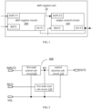
- FIG. 1 is a schematic diagram of a shift register unit according to some embodiments of the present disclosure. As illustrated in FIG. 1 , a shift register unit 10 includes an output control circuit 100 and a shift register circuit 200.
- the shift register circuit 200 includes a first input terminal INPUT1, a first output terminal OUT1, and a first reset terminal RST1.
- the shift register circuit 200 is configured to output a valid output level at the first output terminal OUT1 according to a first input signal received by the first input terminal INPUT1, and is configured to reset according to a first reset signal received by the first reset terminal RST1.
- the output control circuit 100 includes a second input terminal INPUT2, a second output terminal OUT2, and a second reset terminal RST2.
- the second output terminal OUT2 is electrically connected to the first output terminal OUT 1.
- the output control circuit 100 is configured to output an invalid output level at the second output terminal OUT2 according to a second input signal received by the second input terminal INPUT2, thereby controlling a level of the first output terminal OUT1 to the invalid output level, and is configured to reset according to a second reset signal received by the second reset terminal RST2.
- the first output terminal OUT1 and the second output terminal OUT2 are connected to a gate line to drive pixel circuits connected to the gate line.
- the "valid output level" in the shift register unit in the present disclosure refers to a level that enables the switching transistor in the pixel circuit connected thereto to be turned on so that data signals can be written into the pixel circuit
- the "invalid output level” refers to a level that cannot enable the switching transistor in the pixel circuit connected thereto to be turned on (i.e., the switching transistor is turned off).
- the valid output level may be higher or lower than the invalid output level.
- the shift register unit outputs a square wave pulse signal at the output terminal during operation, the valid output level corresponds to the level of the square-wave-pulse portion of the square wave pulse signal, and the invalid output level corresponds to the level of the non-square-wave-pulse portion.
- the second input signal may be an output signal of a first output terminal of a hind shift register unit cascaded with the shift register unit 10 in a gate drive circuit, so that the first output terminal OUT1 of the shift register circuit 200 outputs the invalid output level when the first output terminal of the hind shift register circuit outputs the valid output level, thereby avoiding the multi-output phenomenon of the first output terminal of the shift register circuit.
- the second reset signal may be an output signal of a first output terminal of a front shift register unit cascaded with the shift register unit 10 in the gate drive circuit or a trigger signal of a next frame, so as to ensure that the first output terminal of the shift register unit 10 can normally output during the next scanning, thereby realizing automatic control of the level of the first output terminal of the shift register circuit and ensuring normal display of the display panel.
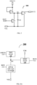
- FIG. 2 is a schematic diagram of an exemplary output control circuit provided by some embodiments of the present disclosure.
- the output control circuit 100 includes a control selection sub-circuit 110, a first node control sub-circuit 120, and a first node reset sub-circuit 130.
- the control selection sub-circuit 110 is configured to output the invalid output level at the second output terminal OUT2 under control of a level of a first node N1, thereby controlling a level of the first output terminal OUT1 to be the invalid output level during a non-output period.
- the control selection sub-circuit 110 can be connected to the first node N1, the second output terminal OUT2, and a first voltage terminal VGL, and is configured to be turned on under control of the level of the first node N1 such that the second output terminal OUT2 is electrically connected to the first voltage terminal VGL to receive a first voltage, and for example, the first voltage is the invalid output level, for example, a low level, thereby controlling the level of the first output terminal OUT1.
- the first node control sub-circuit 120 is configured to charge the first node N1 in response to the second input signal, to adjust the level of the first node N1 to the level which can turn on the control selection sub-circuit 110.
- the first node control sub-circuit 120 is connected to the second input terminal INPUT2, the first node N1, and the first voltage terminal VGL, and is configured to charge the first node N1 under control of the input signal received by the second input terminal INPUT2, to adjust the level of the first node N1 to the level which can turn on the control selection sub-circuit 110.
- the level of the first node N1 is adjusted to the level which can turn on the control selection sub-circuit 110 (for example, the first node N1 is charged), thereby turning on the control selection sub-circuit 110. Therefore, the second output terminal OUT2 is connected to the first voltage terminal VGL to receive the first voltage, so that the output of the first output terminal OUT1 of the shift register circuit 200 can be pulled down to output the invalid output level, thereby avoiding the multi-output phenomenon of the first output terminal of the shift register unit.
- the first node reset sub-circuit 130 is configured to reset the first node N1 in response to the second reset signal.
- the first node reset sub-circuit 130 is connected to the second reset terminal RST2, the first node N1, and the first voltage terminal VGL, and is configured to be turned on under control of the second reset signal received by the second reset terminal RST2, so that the first node N1 is electrically connected to the first voltage terminal VGL, so the first node N1 can be reset and the control selection sub-circuit 110 is turned off, thereby the first output terminal OUT1 of the shift register circuit 200 can normally output.
- the second reset signal may be an output signal of a first output terminal of a front shift register unit cascaded with the shift register unit 10 or a trigger signal of a next frame, so as to ensure that the first output terminal OUT1 of the shift register unit 10 can be out of control of the output control circuit 100 before the next normal output to ensure normal output.
- the first voltage terminal VGL can be configured to keep inputting a direct-current (DC) low level signal, for example, the DC low level signal is referred to as the first voltage, and for example, in the embodiments of the present disclosure, the first voltage is the invalid output level output by the first output terminal, which is same as that in the following embodiments and is not described again.
- DC direct-current
- the output control circuit 100 as illustrated in FIG. 2 may be implemented as the circuit structure as illustrated in FIG. 3 in an example.
- the control selection sub-circuit 110 may be implemented as a first transistor T1, for example.
- a gate electrode of the first transistor T1 is connected to the first node N1 to be turned on under control of the level of the first node N1, a first electrode of the first transistor T1 is connected to the second output terminal OUT2 and is connected to the first output terminal OUT1 of the shift register circuit 200 as well, and a second electrode of the first transistor T1 is connected to the first voltage terminal VGL to receive the first voltage.
- the first node control sub-circuit 120 may be implemented as a second transistor T2 and a first storage capacitor C 1.
- a gate electrode of the second transistor T2 and a first electrode of the second transistor T2 are electrically connected to each other and are both configured to be connected to the second input terminal INPUT2, and a second electrode of the second transistor T2 is configured to be connected to the first node N1.
- a first electrode of the first storage capacitor C1 is connected to the first node N1, and a second electrode of the first storage capacitor C1 is connected to a reference voltage terminal to receive a reference voltage.
- a voltage input at the reference voltage terminal is referred to as a reference voltage
- the reference voltage can be selected according to needs, such as low level (lower than the first voltage), ground, or high level, as long as it can help the first storage capacitor C1 to realize the function of storing electric charges, which is same as that in the following embodiments and is not described again.
- the reference voltage terminal may also be the first voltage terminal VGL, and the embodiments of the present disclosure are not limited thereto.
- the first node reset sub-circuit 130 may be implemented as a third transistor T3.
- a gate electrode of the third transistor T3 is connected to the second reset terminal RST2, a first electrode of the third transistor T3 is connected to the first node N1, and a second electrode of the third transistor T3 is connected to the first voltage terminal VGL to receive the first voltage.
- the first transistor T1, the second transistor T2, and the third transistor T3 are all illustrated by taking N-type transistors as examples, but the embodiments of the present disclosure are not limited thereto and may be implemented at least partially using P-type transistors as required.
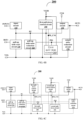
- FIG. 4A is a schematic diagram of a shift register circuit 200 according to some embodiments of the present disclosure.
- the shift register circuit 200 includes an input circuit 210, a pull-up node reset circuit 220, and an output circuit 230.
- the input circuit 210 is configured to charge a pull-up node PU in response to the first input signal.
- the input circuit 210 may be connected to the first input terminal INPUT1 and the pull-up node PU, and is configured to electrically connect the pull-up node PU with the first input terminal INPUT1 under control of the first input signal input by the first input terminal INPUT1 or with a high voltage terminal additionally provided, so that the pull-up node PU can be charged by a high level signal input by the first input terminal INPUT1 or a high level signal output by the high voltage terminal, to raise the voltage of the pull-up node PU to control the output circuit 230 to be turned on.
- the pull-up node reset circuit 220 is configured to reset the pull-up node PU in response to the first reset signal.
- the pull-up node reset circuit 220 may be configured to be connected to the first reset terminal RST1, so that the pull-up node PU can be electrically connected to a low level signal or a low voltage terminal which is the first voltage terminal VGL or the reference voltage terminal for example, under control of the first reset signal input by the first reset terminal RST1, thereby pulling down and resetting the pull-up node PU.
- the output circuit 230 is configured to output a clock signal input from a clock signal terminal CLK to the first output terminal OUT1 under control of the level of the pull-up node PU, and the signal which is output serves as an output signal of the shift register circuit 200 to be input to the second output terminal OUT2 of the output control circuit 100 connected thereto.
- the output circuit 230 may be configured to be turned on under control of the level of the pull-up node PU to electrically connect the clock signal terminal CLK with the first output terminal OUT1, so that the clock signal input by the clock signal terminal CLK can be output to the first output terminal OUT1.
- the shift register circuit 200 may further include a first pull-down circuit 240, a first pull-down control circuit 250, a pull-up node noise reduction circuit 260, and an output noise reduction circuit 270.
- the input circuit 210, the pull-up node reset circuit 220 and the output circuit 230 in this shift register circuit 200 are similar to that in the shift register circuit 200 described in FIG. 4A , and are not described here again.
- the pull-down circuit 240 is configured to control a level of a first pull-down node PD1 under control of levels of the pull-up node PU and a first pull-down control node PD_CN1, thereby controlling the pull-up node noise reduction circuit 260 and the output noise reduction circuit 270.
- the first pull-down circuit 240 may be connected to the first voltage terminal VGL, a second voltage terminal VGH1, the pull-up node PU, the first pull-down node PD1, and the first pull-down control node PD_CN1, and can electrically connect the first pull-down node PD1 with the first voltage terminal VGL under control of the level of the pull-up node PU, so as to pull-down and control the level of the first pull-down node PD1 to a low potential.
- the first pull-down circuit 240 can electrically connect the first pull-down node PD1 with the second voltage terminal VGH1 under control of the level of the first pull-down control node PD_CN1, thereby charging the first pull-down node PD1 to a high potential.
- the first pull-down control circuit 250 is configured to control the level of the first pull-down control node PD_CN1 under control of the level of the pull-up node PU.
- the first pull-down control circuit 250 may be connected to the first voltage terminal VGL, the second voltage terminal VGH1, the pull-up node PU and the first pull-down control node PD_CN1, and can electrically connect the first pull-down control node PD_CN1 with the first voltage terminal VGL under control of the level of the pull-up node PU, thereby controlling the level of the first pull-down control node PD_CN1.
- the shift register circuit 200 may further include a second pull-down circuit 241 and a second pull-down control circuit 251.
- the input circuit 210, the pull-up node reset circuit 220, the output circuit 230, the first pull-down circuit 240, and the first pull-down control circuit 250 in this shift register circuit 200 are similar to that in the shift register circuit 200 described in FIG. 4A and FIG. 4B , and are not described here again.
- the second pull-down circuit 241 is connected to the first voltage terminal VGL, a third voltage terminal VGH2, the pull-up node PU, a second pull-down node PD2, and a second pull-down control node PD_CN2, and can electrically connect the second pull-down node PD2 with the first voltage terminal VGL under control of the level of the pull-up node PU, thereby pulling down and controlling the level of the second pull-down node PD2 to a low potential.
- the second pull-down circuit 241 can electrically connect the second pull-down node PD2 with the third voltage terminal VGH2 under control of the level of the second pull-down control node PD_CN2, thereby charging the second pull-down node PD2 to a high potential.
- the second pull-down control circuit 251 is configured to control the level of the second pull-down control node PD_CN2 under control of the level of the pull-up node PU.
- the second pull-down control circuit 251 is connected to the first voltage terminal VGL, the third voltage terminal VGH2, the pull-up node PU and the second pull-down control node PD_CN2, and can electrically connect the second pull-down control node PD_CN2 with the first voltage terminal VGL under control of the level of the pull-up node PU, thereby controlling the level of the second pull-down control node PD_CN2.
- the pull-up node noise reduction circuit 260 and the output noise reduction circuit 270 in the shift register unit 200 operate under alternating control of the first pull-down node PD1 and the second pull-down node PD2, and the second voltage terminal VGH1 and the third voltage terminal VHG2 are alternately at high levels, so as to reduce the stress of transistors connected to the second voltage terminal VGH1 and the third voltage terminal VGH2 and prolong the service life of the transistors.
- the pull-up node noise reduction circuit 260 is configured to reduce a noise of the pull-up node PU under control of the level of the first pull-down node PD1 or the level of the second pull-down node PD2.
- the pull-up node noise reduction circuit 260 may be configured to be connected to the first voltage terminal VGL to electrically connect the pull-up node PU with the first voltage terminal VGL under control of the level of the first pull-down node PD1 or the level of the second pull-down node PD2, thereby performing pull-down noise reduction on the pull-up node PU.
- the output noise reduction circuit 270 is configured to reduce a noise of the first output terminal OUT1 under control of the level of the first pull-down node PD1 or the level of the second pull-down node PD2.
- the output noise reduction circuit 270 may be configured to electrically connect the first output terminal OUT1 with the first voltage terminal VGL under control of the level of the first pull-down node PD1 or the level of the second pull-down node PD2, thereby performing pull-down noise reduction on the first output terminal OUT1.
- the second voltage terminal VGH1 and the third voltage terminal VGH2 can be configured to alternately input DC high level signals, and for example, the DC high level signal input by the second voltage terminal VGH1 is referred to as a second voltage, and the DC high level signal input by the third voltage terminal VGH2 is referred to as a third voltage.
- the second voltage and the third voltage can be exactly the same voltage, and the second voltage or the third voltage is greater than the first voltage. The following embodiments are the same as this and are not described again.
- the shift register circuit 200 as illustrated in FIG. 4C may be implemented as the circuit structure as illustrated in FIG. 5 in an example.
- each transistor is illustrated as an N-type transistor as an example, which is not limitative to the embodiments of the present disclosure.
- the input circuit 210 may be implemented as a fourth transistor T4.
- a gate electrode of the fourth transistor T4 and a first electrode of the fourth transistor T4 are electrically connected to each other and are both configured to be connected to the first input terminal INPUT1 to receive the first input signal, and a second electrode of the fourth transistor T4 is configured to be connected to the pull-up node PU, so that in a case where the first input signal received by the first input terminal INPUT 1 is a conductive signal (high level signal), the conductive signal is used by the fourth transistor T4 to charge the pull-up node PU to a high level.
- the pull-up node reset circuit 220 may be implemented as a fifth transistor T5.
- a gate electrode of the fifth transistor T5 is configured to be connected to the first reset terminal RST1 to receive the first reset signal
- a first electrode of the fifth transistor T5 is configured to be connected to the pull-up node PU
- a second electrode of the fifth transistor T5 is configured to be connected to the first voltage terminal VGL to receive the first voltage.
- the pull-up node PU and the first voltage terminal VGL are electrically connected, so that the pull-up node PU can be reset to reduce from a high level to a low level.
- the output circuit 230 may be implemented as a sixth transistor T6 and a second storage capacitor C2.
- a gate electrode of the sixth transistor T6 is configured to be connected to the pull-up node PU, a first electrode of the sixth transistor T6 is configured to be connected to the clock signal terminal CLK to receive the clock signal, and a second electrode of the sixth transistor T6 is configured to be connected to the first output terminal OUT1.
- a first electrode of the second storage capacitor C2 is configured to be connected to the gate electrode of the sixth transistor T6, and a second electrode of the second storage capacitor C2 is connected to the second electrode of the sixth transistor T6.
- the first pull-down circuit 240 may be implemented as a seventh transistor T7 and an eighth transistor T8.
- a gate electrode of the seventh transistor T7 is configured to be connected to the first pull-down control node PD_CN1, a first electrode of the seventh transistor T7 is configured to be connected to the second voltage terminal VGH1 to receive the second voltage, and a second electrode of the seventh transistor T7 is configured to be connected to the first pull-down node PD1.
- a gate electrode of the eighth transistor T8 is configured to be connected to the pull-up node PU, a first electrode of the eighth transistor T8 is configured to be connected to the first pull-down node PD1, and a second electrode of the eighth transistor T8 is configured to be connected to the first voltage terminal VGL to receive the first voltage.
- the first pull-down control circuit 250 may be implemented as a ninth transistor T9 and a tenth transistor T10.
- a gate electrode of the ninth transistor T9 and a first electrode of the ninth transistor T9 are electrically connected to each other and are both configured to be connected to the second voltage terminal VGH1 to receive the second voltage, and a second electrode of the ninth transistor T9 is configured to be connected to the first pull-down control node PD_CN1.
- a gate electrode of the tenth transistor T10 is configured to be connected to the pull-up node PU, a first electrode of the tenth transistor T10 is configured to be connected to the first pull-down control node PD_CN1, and a second electrode of the tenth transistor T10 is configured to be connected to the first voltage terminal VGL to receive the first voltage.
- the second pull-down circuit 241 may be implemented as a twenty-seventh transistor T27 and a twenty-eighth transistor T28.
- a gate electrode of the twenty-seventh transistor T27 is configured to be connected to the second pull-down control node PD_CN2
- a first electrode of the twenty-seventh transistor T27 is configured to be connected to the third voltage terminal VGH2 to receive the third voltage
- a second electrode of the twenty-seventh transistor T27 is configured to be connected to the second pull-down node PD2.
- a gate electrode of the twenty-eighth transistor T28 is configured to be connected to the pull-up node PU, a first electrode of the twenty-eighth transistor T28 is configured to be connected to the second pull-down node PD2, and a second electrode of the twenty-eighth transistor T28 is configured to be connected to the first voltage terminal VGL to receive the first voltage.
- the second pull-down control circuit 251 may be implemented as a twenty-ninth transistor T29 and a twentieth transistor T20.
- a gate electrode of the twenty-ninth transistor T29 and a first electrode of the twenty-ninth transistor T29 are electrically connected to each other and are both configured to be connected to the third voltage terminal VGH2 to receive the third voltage, and a second electrode of the twenty-ninth transistor T29 is configured to be connected to the second pull-down control node PD_CN2.
- a gate electrode of the twentieth transistor T20 is configured to be connected to the pull-up node PU, a first electrode of the twentieth transistor T20 is configured to be connected to the second pull-down control node PD_CN2, and a second electrode of the twentieth transistor T20 is configured to be connected to the first voltage terminal VGL to receive the first voltage.
- the pull-up node noise reduction circuit 260 may be implemented as an eleventh transistor T11 and a twenty-first transistor T21.
- a gate electrode of the eleventh transistor T11 is configured to be connected to the first pull-down node PD1
- a first electrode of the eleventh transistor T11 is configured to be connected to the pull-up node PU
- a second electrode of the eleventh transistor T11 is configured to be connected to the first voltage terminal VGL to receive the first voltage.
- the eleventh transistor T11 is turned on in a case where the first pull-down node PD1 is at a high potential, and the pull-up node PU is connected to the first voltage terminal VGL, so that the pull-up node PU can be pulled down to realize noise reduction.
- a gate electrode of the twenty-first transistor T21 is configured to be connected to the second pull-down node PD2, a first electrode of the twenty-first transistor T21 is configured to be connected to the pull-up node PU, and a second electrode of the twenty-first transistor T21 is configured to be connected to the first voltage terminal VGL to receive the first voltage.
- the twenty-first transistor T21 is turned on in a case where the second pull-down node PD2 is at a high potential, and the pull-up node PU is connected to the first voltage terminal VGL, so that the pull-up node PU can be pulled down to realize noise reduction.
- the output noise reduction circuit 270 may be implemented as a twelfth transistor T12 and a twenty-second transistor T22.
- a gate electrode of the twelfth transistor T12 is configured to be connected to the first pull-down node PD1
- a first electrode of the twelfth transistor T12 is configured to be connected to the first output terminal OUT1
- a second electrode of the twelfth transistor T12 is configured to be connected to the first voltage terminal VGL to receive the first voltage.
- the twelfth transistor T12 is turned on in a case where the first pull-down node PD1 is at a high potential, and the first output terminal OUT1 is connected to the first voltage terminal VGL, so that the noise can be reduced at the first output terminal OUT1.
- a gate electrode of the twenty-second transistor T22 is configured to be connected to the second pull-down node PD2, a first electrode of the twenty-second transistor T22 is configured to be connected to the first output terminal OUT1, and a second electrode of the twenty-second transistor T22 is configured to be connected to the first voltage terminal VGL to receive the first voltage.
- the twenty-second transistor T22 is turned on in a case where the second pull-down node PD2 is at a high potential, and the first output terminal OUT1 is connected to the first voltage terminal VGL, so that the noise can be reduced at the first output terminal OUT1.
- the first node N1, the pull-up node PU, the first pull-down node PD1, the second pull-down node PD2, the first pull-down control node PD_CN1, and the second pull-down control node PD_CN2 do not represent actual components, but represent the junction points of related electrical connections in the circuit diagram.
- the transistors used in the embodiments of the present disclosure can be thin film transistors, field effect transistors, or other switching devices with the same characteristics, and the embodiments of the present disclosure are all described with thin film transistors as examples.
- the source electrode and drain electrode of the transistor used here can be symmetrical in structure, so the source electrode and drain electrode can be structurally indistinguishable.
- one electrode is directly described as the first electrode and the other electrode is described as the second electrode.
- the transistors in the embodiments of the present disclosure are all described by taking N-type transistors as examples, in which the first electrode of the transistor is the drain electrode and the second electrode is the source electrode.
- the present disclosure includes but is not limited to this.
- one or more transistors in the shift register unit provided by the embodiments of the present disclosure may also adopt P-type transistors.
- the first electrode of the transistor is the source electrode and the second electrode is the drain electrode, as long as the polarities of the respective electrodes of the selected type of transistors are correspondingly connected according to the polarities of the respective electrodes of the respective transistors in the embodiments of the present disclosure, and the respective voltage terminals provide corresponding high voltages or low voltages.
- indium gallium zinc oxide IGZO
- LTPS low temperature polysilicon
- amorphous silicon such as hydrogenated amorphous silicon
- the term "pull-up” means charging a node or an electrode of a transistor so as to raise the absolute value of the level of the node or the electrode, thereby realizing the operation (e.g., turn-on) of the corresponding transistor; and the term “pull-down” means discharging a node or an electrode of a transistor so as to reduce the absolute value of the level of the node or the electrode, thereby realizing the operation (e.g., turn-off) of the corresponding transistor.
- pulse-up means discharging a node or an electrode of a transistor so as to reduce the absolute value of the level of the node or the electrode, thereby realizing the operation (e.g., turn-on) of the corresponding transistor
- pulse-down means charging a node or an electrode of a transistor so as to raise the absolute value of the level of the node or the electrode, thereby realizing the operation (e.g., turn-off) of the corresponding transistor.
- the transistors in the shift register circuit 200 are all N-type transistors.
- the first voltage terminal VGL maintains inputting a first voltage of DC low level
- the second voltage terminal VGH1 and the third voltage terminal VGH2 alternately input a second voltage and a third voltage of DC high level
- the clock signal terminal CLK inputs a clock signal.
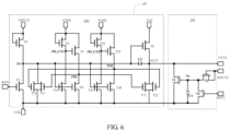
- FIG. 6 is a circuit schematic diagram of a specific implementation example of the shift register unit as illustrated in FIG. 1 .
- the shift register unit 10 includes an output control circuit 100 and a shift register circuit 200.
- the output control circuit 100 adopts a circuit structure as illustrated in FIG. 3
- the shift register circuit 200 adopts a circuit structure as illustrated in FIG. 5 .
- the connection relationship between the output control circuit 100 and the shift register circuit 200 is illustrated in FIG. 6 , and the first output terminal OUT1 and the second output terminal OUT2 are electrically connected to each other.
- shift register circuit 200 in the embodiments of the present disclosure is not limited to the examples described above, and any shift register circuit that can be cascaded to form a gate drive circuit to output multi-level scanning signals can be applied in the embodiments of the present disclosure.
- the embodiments of the present disclosure provide a gate drive circuit 20, which includes a plurality of shift register units 10 that are cascaded.
- each shift register unit 10 is described taking the circuit structure illustrated in FIG. 6 as an example, but the embodiments of the present disclosure are not limited thereto.
- the gate drive circuit 20 further includes 2m (m is an integer greater than 0) clock signal lines which are configured to supply clock signals to each shift register unit.
- the gate drive circuit 20 illustrated in FIG. 7A or FIG. 8A includes two clock signal lines, therefore, in this case, m is equal to 1; and the gate drive circuit 20 illustrated in FIG. 9A includes four clock signal lines, therefore, in this case, m is equal to 2.
- a second input terminal INPUT2 of other shift register units is connected to a first output terminal OUT1 of a hind shift register unit which is separated by m-1 shift register units.
- m-1 shift register units are closely adjacent.
- a second input terminal INPUT2 of other shift register units is connected to a first output terminal OUT1 of a hinder shift register unit, that is, connected to the first output terminal OUT1 of the hinder shift register unit which is separated by 0 shift register unit.
- the gate drive circuit 20 is connected in such a way that, except for the last two shift register units, a second input terminal INPUT2 of other shift register units is connected to a first output terminal OUT1 of a hind shift register unit which is separated by one shift register unit.
- input signals may be separately supplied thereto, or they may be sequentially connected to the first output terminals OUT1 of the first to mth shift register units.
- a second input signal may be separately provided to the second input terminal INPUT2 of the last shift register unit, or the second input terminal INPUT2 of the last shift register unit may be connected to the first output terminal OUT1 of the first shift register unit.
- the gate drive circuit 20 illustrated in FIG. 7A or FIG. 8A a second input signal may be separately provided to the second input terminal INPUT2 of the last shift register unit, or the second input terminal INPUT2 of the last shift register unit may be connected to the first output terminal OUT1 of the first shift register unit.
- second input signals may be separately provided to the second input terminals INPUT2 of the last two shift register units, or the second input terminals INPUT2 of the last two shift register units may be sequentially connected to the first output terminals OUT1 of the first to second shift register units, and for example, the second input terminal INPUT2 of the last shift register unit is connected to the first output terminal OUT1 of the second shift register unit, and the second input terminal INPUT2 of the last second shift register unit is connected to the first output terminal OUT1 of the first shift register unit.
- the first input terminal INPUT1 of each of other shift register units is connected to the first output terminal OUT1 of a front shift register unit which is separated by m-1 shift register units, and first input signals can be separately provided for the first input terminals INPUT1 of the first to mth shift register units.
- the first input terminals INPUT1 of the first to mth shift register units can be connected to the first output terminals OUT1 of the last m shift register units in sequence.
- connection mode of the first or the first to mth shift register units is same as that of the second reset terminal RST2 of the same shift register units, which is described in detail below. Except for the last m shift register units, the first reset terminal RST1 of each of the other shift register units is connected to the first output terminal OUT1 of the hind shift register unit which is separated by m-1 shift register units.
- the first reset terminals RST1 of the last m shift register units may be separately provided with reset signals (e.g., same as the second input signal of the second input terminal INPUT2 of the same shift register unit), or the first reset terminals RST1 of the last m shift register units may be sequentially connected to the first output terminals OUT1 of the first to mth shift register units, e.g., the connection mode thereof is same as the connection mode of the second input terminal INPUT2 of the same shift register unit, and is not repeated here.
- the second reset terminal RST2 of the output control circuit 100 of each shift register unit is connected to a trigger signal line STV1, for example, as illustrated in FIG. 7A .
- the second reset terminal RST2 of the output control circuit 100 of each of the other shift register units is connected to the first output terminal OUT1 of the front shift register unit which is separated by m-1 shift register units.
- the second reset signals may be separately provided for the second reset terminals RST2 of the first to mth shift register units (e.g., same as the signal of the first input terminal INPUT 1 of the same shift register unit), or the second reset terminals RST2 of the first to mth shift register units may be connected in sequence to the first output terminals OUT1 of the last m shift register units.
- this example includes two clock signal lines, i.e., m is equal to 1.
- the second reset terminal RST2 of the output control circuit 100 of each of the other shift register units is connected to the first output terminal OUT1 of the adjacent front shift register unit, i.e., connected to the first output terminal OUT1 of the front shift register unit which is separated by 0 shift register unit.
- the second reset signal may be separately provided to the second reset terminal RST2 of the first shift register unit (e.g., same as the signal of the first input terminal INPUT1 of the same shift register unit), or the second reset terminal RST2 of the first shift register unit may be connected to the first output terminal OUT1 of the last shift register unit. For example, as illustrated in FIG.
- the second reset terminal RST2 of the output control circuit 100 of each of the other shift register units is connected to the first output terminal OUT1 of the front shift register unit which is separated by one shift register unit.
- the second reset signals may be separately provided for the second reset terminals RST2 of the first and second shift register units (e.g., same as that the signal of the first input terminal INPUT1 of the same shift register unit), or the second reset terminals RST2 of the first and second shift register units are connected to the first output terminals OUT1 of the last two shift register units in sequence, and for example, the second reset terminal RST2 of the first shift register unit is connected to the first output terminal OUT1 of the last second shift register unit, and the second reset terminal RST2 of the second shift register unit is connected to the first output terminal OUT1 of the last shift register unit.
- an example of the embodiments of the present disclosure provides a gate drive circuit 20, which includes a plurality of shift register units 10 that are cascaded, a first clock signal line CLK1, a second clock signal line CLK2, and a trigger signal line STV1.
- each shift register unit 10 adopts the circuit structure as illustrated in FIG. 6 .
- the gate drive circuit 20 may further include four, six or eight clock signal lines, the number of which depends on the specific situations, and the embodiments of the present disclosure are not limited thereto.
- each of the shift register units further includes a clock signal terminal CLK and is configured to be connected to the first clock signal line CLK1 or the second clock signal line CLK2 to receive a first clock signal or a second clock signal.
- the first clock signal line CLK1 is connected to clock signal terminals CLK of (2n-1)th (n is an integer greater than 0) shift register units
- the second clock signal line CLK2 is connected to clock signal terminals CLK of (2n)th shift register units.
- the embodiments of the present disclosure include but are not limited to the above-mentioned connection mode.
- the first clock signal line CLK1 may be connected to the clock signal terminals CLK of the (2n)th (n is an integer greater than 0) shift register units
- the second clock signal line CLK2 may be connected to the clock signal terminals CLK of the (2n-1)th shift register units.
- OUT1_N-1 illustrated in FIG. 7A represents a first output terminal of (N-1)th shift register unit
- OUT1_N represents a first output terminal of Nth shift register unit
- OUT1_N+1 represents a first output terminal of (N+1)th shift register unit
- OUT2_N-1 illustrated in FIG. 7A represents a second output terminal of an output control circuit of the (N-1)th shift register unit
- OUT2_N represents a second output terminal of an output control circuit of the Nth shift register unit
- OUT2_N+1 represents a second output terminal of an output control circuit of the (N+1)th shift register unit, and so on.
- the reference numerals in the following embodiments are similar to this and are not repeated again.
- the gate drive circuit 20 may further include a timing controller 300.
- the timing controller 300 may be configured to be connected to the trigger signal line STV1, the first clock signal line CLK1, and the second clock signal line CLK2, to provide trigger signals and clock signals to each shift register unit.
- the timing controller 300 may also be configured to provide reset signals.
- the second input terminal INPUT2 of each of the other shift register units is connected to the first output terminal OUT1 of the adjacent hind shift register unit.
- the second input terminal INPUT2 of the last shift register unit may be separately provided with an input signal, or the second input terminal INPUT2 of the last shift register unit may be connected to the first output terminal OUT1 of the first shift register unit.
- the first reset terminal RST1 of each of the other shift register units is connected to the first output terminal OUT1 of the adjacent hind shift register unit.
- the first input terminal INPUT1 of each of the other shift register units is connected to the first output terminal OUT1 of the adjacent front shift register unit.
- the second reset terminal RST2 of the output control circuit 100 of each shift register unit is connected to the trigger signal line STV1 to receive the trigger signal, so as to simultaneously reset the first node N1 of the output control circuit 100 of each shift register unit when a frame starts scanning, thus ensuring that the Nth shift register unit resets the first node N1 of the Nth shift register unit in response to the second reset signal before the first output terminal OUT1 of the shift register circuit 200 of the Nth shift register unit enters the period when the valid output level is output, thereby not affecting the normal output of each shift register circuit.
- the second reset signal is the trigger signal.
- the first input INPUT1 of the first shift register unit may be connected to the trigger signal line STV1 and configured to receive the trigger signal STV, or be connected to the first output OUT1 of the last shift register unit.
- the first reset terminal RST1 of the last shift register unit may be configured to receive a separately provided first reset signal RESET1 (e.g., same as the signal of the second input terminal INPUT2 of the same shift register unit), or be connected to the first output terminal OUT1 of the first shift register unit, which is not illustrated in FIG. 7A for the sake of brevity.
- a shift register unit B is a hind shift register unit of another shift register unit A, indicates that a gate scanning signal output by the shift register unit B is later in timing than a gate scanning signal output by the shift register unit A.
- a shift register unit B is a front shift register unit of another shift register unit A, indicates that a gate scanning signal output by the shift register unit B is earlier in timing than a gate scanning signal output by the shift register unit A.
- the clock signal timing provided by the trigger signal line STV1, the first clock signal line CLK1, and the second clock signal line CLK2 may adopt the signal timing illustrated in FIG. 7B , to realize the function of outputting gate scanning signals row by row by the gate drive circuit 20.
- STV1, CLK1, CLK2, VGH1, VGH2, OUT1_N, N1, OUT2_N and OUT1_N+1 represent not only corresponding signal terminals or signal lines, but also corresponding signals.
- the valid output level is a high level and the invalid output level is a low level.
- the first clock signal CLK1 and the second clock signal CLK2 are complementary to each other.
- the gate drive circuit 20 can perform following operations respectively.
- the embodiments of the present disclosure take the working principle of the Nth shift register unit in the gate drive circuit 20 as an example, and the working principle of the other shift register units is the same and is not described again.
- the Nth shift register unit includes an Nth shift register circuit and an Nth output control circuit.
- an Nth frame is a phase of outputting the gate scanning signals row by row
- an (N+1)th frame is a phase of outputting the gate scanning signals row by row next to the Nth frame.
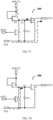
- FIG. 7C is a schematic diagram in a case where the output control circuit 100 as illustrated in FIG. 3 is in the second phase 2
- FIG. 7D is a schematic diagram in a case where the output control circuit 100 as illustrated in FIG. 3 is in the third phase 3.
- transistors identified by dashed lines in FIG. 7C and FIG. 7D both indicate that they are in a turn-off state in the corresponding phases
- dashed lines with arrows in FIG. 7C and FIG.7D indicate the current direction of the output control circuit 100 in the corresponding phases.
- the transistors as illustrated in FIG. 7C and FIG. 7D are explained by taking N-type transistors as an example, i.e., the gate electrode of each transistor is turned on when a high level is provided, and is turned off when a low level is provided.
- the trigger signal line STV1 provides a low level signal
- the first clock signal line CLK1 provides a high level signal. Because the clock signal terminal CLK of the Nth shift register unit is connected to the first clock signal line CLK1, the high level signal input by the clock signal terminal CLK is output to the first output terminal OUT1_N of the Nth shift register unit during this phase.
- the high level is referred to as a valid output level, that is, the first output terminal OUT1 of the Nth shift register unit is in a period when the valid output level is output during this phase.
- the second clock signal line CLK2 provides a low level signal.
- the clock signal terminal CLK of the (N+1)th shift register unit is connected to the second clock signal line CLK2, the low level signal input by the clock signal terminal CLK during this phase is output to the first output terminal OUT1_N+1 of the (N+1)th shift register unit.
- the output control circuit 100 is in a turn-off state during this phase, and because the second output terminal OUT2_N of the output control circuit 100 of the Nth shift register unit is connected to the first output terminal OUT1_N of the shift register circuit 200 of the Nth shift register unit, the second output terminal OUT2_N of the output control circuit 100 of the Nth shift register unit outputs a high level signal during this phase.
- the level of potential in the signal timing as illustrated in FIG. 7B is only schematic and does not represent the true potential value or relative proportion.
- the high level signal corresponds to the turn-on signal of the N-type transistor, while the low level signal corresponds to the turn-off signal of the N-type transistor.
- the trigger signal line STV1 provides a low level signal and the first clock signal line CLK1 provides a low level signal. Because the clock signal terminal CLK of the Nth shift register unit is connected to the first clock signal line CLK1, the low level signal input by the clock signal terminal CLK is output to the first output terminal OUT1_N of the Nth shift register unit during this phase.
- the low level is referred to as an invalid output level, that is, the first output terminal OUT1 of the Nth shift register unit is in a period when the invalid output level is output during this phase.
- the second clock signal line CLK2 provides a high level signal.
- the clock signal terminal CLK of the (N+1)th shift register unit is connected to the second clock signal line CLK2
- the high level signal input by the clock signal terminal CLK is output to the first output terminal OUT1_N+1 of the (N+1)th shift register unit during this phase. Therefore, during this phase, the first output terminal OUT1 of the (N+1)th shift register unit is in a period when the valid output level is output.
- the second input terminal INPUT2 of the Nth output control circuit 100 receives a high level signal.
- the second transistor T2 is turned on in response to the input high level signal received by the second input terminal INPUT2
- the first transistor T1 is turned on in response to the high level of the first node N1
- the third transistor T3 is turned off in response to the low level of the trigger signal.
- a charging path of the first node N1 (as illustrated by the dashed line 1 with an arrow in FIG. 7C ) and an output path of the invalid output level of the second output terminal OUT2 (as illustrated by the dashed line 2 with an arrow in FIG. 7C ) are formed in the output control circuit 100 as illustrated in FIG. 3 . Because the second transistor T2 is turned on, the valid output level of the first output terminal OUT1_N+1 of the (N+1)th shift register unit received at the second input terminal INPUT2 charges the first node N1 to a high level.
- the first transistor T1 is turned on under control of the high level of the first node N1, so that the second output terminal OUT2 of the output control circuit 100 of the Nth shift register unit is connected to the first voltage terminal VGL, thus the second output terminal OUT2 outputs a first voltage, i.e., outputs the invalid output level. Because in the Nth shift register unit, the second output terminal OUT2_N is connected to the first output terminal OUT1_N, the output of the first output terminal OUT1_N of the shift register circuit 200 of the Nth shift register unit is also pulled down to output the invalid output level, and therefore, the first output terminal OUT1_N of the Nth shift register unit enters a period when the valid output level is output.
- the (N+1)th frame starts scanning, while the first output terminal OUT1_N of the shift register circuit 200 of the Nth shift register unit is still in the period when the invalid output level is output.
- the trigger signal line STV1 provides a high level signal. Because the second reset terminal RST2 of the Nth output control circuit 100 is connected to the trigger signal line STV1, the first node reset sub-circuits 130 of the output control circuits 100 of all shift register units are turned on during this phase.
- the third transistor T3 is turned on in response to the second reset signal (i.e., the trigger signal) received by the second reset terminal RST2, the first transistor T1 is turned off under control of the low level of the first node N1, and the second transistor T2 is turned off under control of the second input signal input by the second input terminal INPUT2.
- the second reset signal i.e., the trigger signal
- a reset path of the first node N1 (as illustrated by the dashed line with an arrow in FIG. 7D ) is formed in the output control circuit 100 as illustrated in FIG. 3 . Because the third transistor T3 is turned on, the first node N1 is connected to the first voltage terminal VGL, and the first node N1 is discharged to the first voltage (low level).
- both the first electrode and the second electrode of the first storage capacitor C1 are connected to the first voltage terminal VGL, so the first storage capacitor C1 is discharged and continues to stabilize the voltage of the first node N1, so that the first transistor T1 is turned off under control of the level of the first node N1, so as to close the control on the first output terminal OUT1 of the shift register unit and ensure that the first output terminal OUT1 of each shift register unit can normally output the valid output level during the (N+1)th frame scanning.
- FIG. 8A is another example of a gate drive circuit 20 provided by some embodiments of the present disclosure.
- the gate drive circuit 20 as illustrated in FIG. 8A is similar in structure to the gate drive circuit 20 as illustrated in FIG. 7A , except followings: in the gate drive circuit 20, except for the first output control circuit 100, the second reset terminal RST2 of each of the other output control circuits 100 is connected to the first output terminal OUT1 of the adjacent front shift register unit; the second reset terminal RST2 of the output control circuit 100 of the first shift register unit can be configured to receive a second reset signal RESET2 that is separately provided or be connected to the first output terminal OUT1 of the last shift register unit, thereby ensuring that the Nth shift register unit resets the first node N1 of the Nth shift register unit in response to the second reset signal before the first output terminal OUT1 of the shift register circuit 200 of the Nth shift register unit enters the period when the valid output level is output.
- the second reset signal is the output signal of the first output terminal OUT1 of the adjacent front shift register unit. It should be noted that the trigger signal line STV1 and the second reset signal RESET2 are not illustrated in FIG. 8A for the sake of brevity.
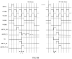
- the timing of the trigger signal and the clock signals provided by the trigger signal line STV1, the first clock signal line CLK1, and the second clock signal line CLK2 may adopt the signal timing as illustrated in FIG. 8B , to realize the function of outputting gate scanning signals row by row by the gate drive circuit 20.
- the operation principle of the gate drive circuit 20 as illustrated in FIG. 8A is described below with reference to the signal timing as illustrated in FIG. 8B .
- the valid output level is a high level and the invalid output level is a low level.
- the first clock signal CLK1 and the second clock signal CLK2 are complementary to each other.
- the gate drive circuit 20 can perform following operations respectively.
- the operation principle of the gate drive circuit 20 illustrated in FIG. 8A is similar to that of the gate drive circuit illustrated in FIG. 7A , except for the third phase 3. Therefore, similar parts are not described in detail, and the specific operation process of the gate drive circuit 20 during the third phase 3 is described below.
- the second clock signal line CLK2 provides a high level signal. Because the clock signal terminal CLK of the (N-1)th shift register unit is connected to the second clock signal line CLK2, the high level signal input by the clock signal terminal CLK is output to the first output terminal OUT1_N-1 of the (N-1)th shift register unit during this phase. Therefore, in this phase, the first output terminal OUT1_N-1 of the (N-1)th shift register unit is in a period when the valid output level is output.
- the first node reset sub-circuit of the output control circuit of the Nth shift register unit is turned on during this phase to reset the first node, thus not affecting the normal output of the Nth shift register circuit cascaded with the (N-1)th shift register unit.
- An embodiment of the present disclosure also provides a gate drive circuit 20.
- the gate drive circuit 20 includes a plurality of shift register units 10 that are cascaded, a first clock signal line CLK1, a second clock signal line CLK2, a third clock signal line CLK3, and a fourth clock signal line CLK4.
- each shift register unit 10 adopts the circuit structure as illustrated in FIG. 6 .
- each of the shift register circuits 200 in the plurality of shift register units further includes a clock signal terminal CLK, and is configured to be connected to a corresponding clock signal line to receive a first clock signal, a second clock signal, a third clock signal, or a fourth clock signal according to an order in the cascaded shift register units.
- the first clock signal line CLK1 is connected to, for example, clock signal terminals CLK of (4n-3)th (n is an integer greater than 0) shift register units;
- the second clock signal line CLK2 is connected to, for example, clock signal terminals CLK of (4n-2)th shift register units;
- the third clock signal line CLK3 is connected to, for example, clock signal terminals CLK of (4n-1)th shift register units;
- the fourth clock signal line CLK4 is connected to, for example, clock signal terminals CLK of (4n)th shift register units.
- a second input terminal INPUT2 of each of other shift register units is connected to a first output terminal OUT1 of a hind shift register unit which is separated by one shift register unit.
- second input terminals INPUT2 of the last two shift register units may be configured to receive separately provided second input signals, or, the second input terminal INPUT2 of the last shift register unit is connected to a first output terminal OUT1 of a second shift register unit, and the second input terminal INPUT2 of the last second shift register unit is connected to a first output terminal OUT1 of a first shift register unit.
- a first input terminal INPUT 1 of other shift register units is connected to a first output terminal OUT1 of a front shift register unit which is separated by one shift register unit; and except for the last two shift register units, a first reset terminal RST1 of the other shift register units is connected to the first output terminal OUT1 of the hind shift register unit which is separated by one shift register unit.
- a second reset terminal RST2 of an output control circuit 100 of the other shift register units is connected to the first output terminal OUT1 of the front shift register unit which is separated by one shift register unit.
- second reset terminals RST2 of the first and second shift register units may be configured to receive separately provided second reset signals, or, the second reset terminal RST2 of the first shift register unit is connected to the first output terminal OUT1 of the last second shift register unit, and the second reset terminal RST2 of the second shift register unit is connected to the first output terminal OUT1 of the last shift register unit.
- first input terminals INPUT 1 of the first and second shift register units may be configured to receive the trigger signal STV1, or, the first input terminal INPUT1 of the first shift register unit is connected to the first output terminal OUT1 of the last second shift register unit, and the first input terminal INPUT1 of the second shift register unit is connected to the first output terminal OUT1 of the last shift register unit.
- First reset terminals RST1 of the last two shift register units may be configured to receive a separately provided first reset signal RESET1, or, the first reset terminal RST1 of the last second shift register unit may be connected to the first output terminal OUT1 of the first shift register unit, and the first reset terminal RST1 of the last shift register unit may be connected to the first output terminal OUT1 of the second shift register unit.
- the trigger signal STV1 and the first reset signal RESET1 are not illustrated in FIG. 9A .
- the gate drive circuit 20 may further include a timing controller 300.
- the timing controller 300 may be configured to be connected to the first clock signal line CLK1, the second clock signal line CLK2, the third clock signal line CLK3, and the fourth clock signal line CLK4, to provide touch scanning control signals and clock signals to each shift register unit.
- the timing controller 300 may also be configured to provide the trigger signal STV1 and the reset signal.
- the trigger signal STV1 is provided by the trigger signal line STV1, which is not illustrated in FIG. 9A for the sake of brevity.
- the timing of the trigger signal and the clock signals provided by the trigger signal line STV1, the first clock signal line CLK1, the second clock signal line CLK2, the third clock signal line CLK3, and the fourth clock signal line CLK4 may adopt the signal timing as illustrated in FIG. 9B , to realize the function of outputting gate scanning signals row by row by the gate drive circuit 20.
- the clock signal on the clock signal line may be attenuated during transmission, which may cause insufficient charging voltage to latter gate lines.
- the load on each clock signal line can be reduced by providing clock signals to each shift register unit of the gate drive circuit through a plurality of clock signal lines, thereby improving the charging rate.
- gate drive circuit 20 provided in the embodiments of the present disclosure may further include six, eight, and more clock signal lines, and the embodiments of the present disclosure are not limited thereto.
- the valid output level is a high level and the invalid output level is a low level.
- the first clock signal CLK1 to the fourth clock signal CLK4 are sequentially delayed by 1/2 square wave width, the first clock signal CLK1 and the third clock signal CLK3 are complementary to each other, and the second clock signal CLK2 and the fourth clock signal CLK4 are complementary to each other.
- the gate drive circuit 20 can perform following operations respectively. It should be noted that the embodiments of the present disclosure take the working principle of the (N+1)th shift register unit as an example, and the working principle of other shift register units is similar to this and is not described again.
- the third clock signal line CLK3 provides a high level signal. Because the clock signal terminal CLK of the (N+1)th shift register unit is connected to the third clock signal line CLK3, the high level signal input by the clock signal terminal CLK is output to the first output terminal OUT1_N+1 of the (N+1)th shift register unit during this phase.
- the high level is referred to as the valid output level, that is, the first output terminal OUT1_N+1 of the (N+1)th shift register unit is in the period when the valid output level is output.
- the first clock signal line CLK1 provides a low level signal.
- the clock signal terminal CLK of the (N+3)th shift register unit (not illustrated in the figure) is connected to the first clock signal line CLK1
- the low level signal input by the clock signal terminal CLK is output to the first output terminal OUT1_N+3 of the (N+3)th shift register unit during this phase.
- the second input terminal INPUT2 of the (N+1)th output control circuit 100 is connected to the first output terminal OUT1_N+3 of the (N+3)th shift register unit, the output control circuit 100 is in a turn-off state during this phase.
- the second output terminal OUT2_N+1 of the output control circuit 100 of the (N+1)th shift register unit is connected to the first output terminal OUT1_N+1 of the shift register circuit 200 of the (N+1)th shift register unit, the second output terminal OUT2_N+1 of the output control circuit 100 of the (N+1)th shift register unit outputs a high level signal during this phase.
- the level of potential in the signal timing as illustrated in FIG. 9B is only schematic and does not represent the true potential value or relative proportion.
- the high level signal corresponds to the turn-on signal of the N-type transistor
- the low level signal corresponds to the turn-off signal of the N-type transistor.
- the fourth clock signal line CLK4 provides a high level signal. Because the clock signal terminal CLK of the (N+2)th shift register unit is connected to the fourth clock signal line CLK4, the high level signal input by the clock signal terminal CLK is output to the first output terminal OUT1_N+2 of the (N+2)th shift register unit during this phase. Therefore, the first output terminal OUT1_N+2 of the (N+2)th shift register unit is in the period when the valid output level is output.
- the third clock signal line CLK3 provides a low level signal. Because the clock signal terminal CLK of the (N+1)th shift register unit is connected to the third clock signal line CLK3, the low level signal input by the clock signal terminal CLK is output to the first output terminal OUT1_N+1 of the (N+1)th shift register unit during this phase.
- the low level is referred to as the invalid output level, i.e., in this phase, the first output terminal OUT1_N+1 of the (N+1)th shift register unit is in the period when the invalid output level is output.
- the first clock signal line CLK1 provides a high level signal.
- the clock signal terminal CLK of the (N+3)th shift register unit is connected to the first clock signal line CLK1
- the high level signal input by the clock signal terminal CLK is output to the first output terminal OUT1_N+3 of the (N+3)th shift register unit during this phase. Therefore, the first output terminal OUT1_N+3 of the (N+3)th shift register unit is in the period when the valid output level is output.
- the second input terminal INPUT2 of the (N+1)th shift register unit Because the second input terminal INPUT2 of the (N+1)th shift register unit is connected to the first output terminal OUT1_N+1 of the (N+3)th shift register unit, the second input terminal INPUT2 of the (N+1)th shift register unit receives a high level signal, thereby charging the first node N1 to ensure that the first output terminal OUT_N+1 of the (N+1)th shift register unit enters the period when the invalid output signal is output.
- the operation process when the second input terminal INPUT2 of the (N+1)th shift register unit receives the high level signal is similar to the operation principle of the output control circuit 100 as illustrated in FIG. 7C , and is not described here again.
- the first clock signal line CLK1 provides a high level signal. Because the clock signal terminal CLK of the (N-1)th shift register unit is connected to the first clock signal line CLK1, the high level signal input by the clock signal terminal CLK is output to the first output terminal OUT1_N-1 of the (N-1)th shift register unit during this phase. Therefore, the first output terminal OUT1_N-1 of the (N-1)th shift register unit is in the period when the valid output level is output in this phase.
- the second reset terminal RST2 of the (N+1)th shift register unit receives a high level signal, thereby resetting the first node N1_N+1 of the (N+1)th shift register unit before the first output terminal OUT1_N+1 of the shift register circuit of the (N+1)th shift register unit enters the period when the valid output level is output, thereby ensuring the normal output of the (N+1)th shift register unit.
- the operation process of the second reset terminal RST2 of the (N+1)th shift register unit when receiving the high level signal is similar to the operation principle of the output control circuit 100 as illustrated in FIG. 7D , and is not repeated here.
- the second clock signal line CLK2 provides a high level signal, and the Nth shift register unit enters the period when the valid output level is output.
- the third clock signal line CLK3 provides a high level signal, and the (N+1)th shift register unit enters the period when the valid output level is output.
- the gate drive circuit 20 may be disposed on a side of the display panel.
- the display panel includes a plurality of rows of gate lines, each row of gate lines is, for example, used to drive pixel circuits of a row of pixel units, gate electrodes of switching transistors of the pixel circuits are connected to the gate lines, and the first output terminal OUT1 or the second output terminal OUT2 of each shift register unit in the gate drive circuit 20 may be configured to be sequentially connected to the plurality of rows of gate lines for outputting gate scanning signals.
- the gate drive circuits 20 may be provided on both sides of the display panel to realize double-sided driving, and the embodiments of the present disclosure do not limit the arrangement of the gate drive circuits 20.
- the embodiments of the present disclosure also provide a display device 1.
- the display device 1 includes the gate drive circuit 20 provided by the embodiments of the present disclosure.
- the display device 1 includes a pixel array comprising a plurality of pixel units 40.
- the display device 1 may further include a data drive circuit 30.
- the data drive circuit 30 is used to provide data signals for the pixel array; and the gate drive circuit 20 is used to provide gate scanning signals for the pixel array.
- the data drive circuit 30 is electrically connected to the pixel units 40 through data lines 31, and the gate drive circuit 20 is specifically implemented as a GOA, for example, directly prepared on the array substrate of the display device 1 and electrically connected to the pixel units 40 through gate lines 21.
- the display device 1 in this embodiment may be any product or component having a display function such as a liquid crystal panel, a liquid crystal television, a display, an organic light-emitting diode (OLED) panel, an OLED TV, an electronic paper display device, a mobile phone, a tablet computer, a notebook computer, a digital photo frame, a navigator, etc.
- the display device 1 may also include other conventional components such as a display panel, and the embodiments of the present disclosure are not limited thereto.
- the technical effect of the display device 1 provided by the embodiments of the present disclosure may be referred to the corresponding description of the gate drive circuit 20 in the above embodiments, and is not described here again.
- An embodiment of the present disclosure also provides a method of driving a gate drive circuit of a display device for example, which may include following operations:
- controlling the second output terminal of the output control circuit of the Nth shift register unit to output the invalid output level includes: during the period when the first output terminal of the shift register circuit of the Nth shift register unit does not output the valid output level, a third transistor T3 being turned off under control of the second reset signal, and a second transistor T2 being turned on in response to the second input signal received by the second input terminal, thereby controlling a level of a first node N1 (e.g., charging the first node N1) such that a first transistor T1 is turned on under control of the level of the first node N1, to connect the second output terminal to a first voltage terminal VGL, so as to control the second output terminal to output the invalid output level.
- a first node N1 e.g., charging the first node N1
- Resetting the first node of the output control circuit of the Nth shift register unit before the first output terminal of the shift register circuit of the Nth shift register unit enters the period when the valid output level is output includes: before the first output terminal of the shift register circuit of the Nth shift register unit enters the period when the valid output level is output, the second transistor T2 being turned off under control of the second input signal received by the second input terminal, the third transistor T3 being turned on under control of the second reset signal so that the first node N1 is connected to the first voltage terminal VGL, thereby resetting the first node N1, so the first transistor T1 is turned off under control of the level of the first node N1.
- the gate drive circuit includes 2m clock signal lines, and the method may more specifically include following operations sequentially:
- m is equal to 1; and for the example as illustrated in FIG. 9A , in a case where four clock signal lines are included, m is equal to 2. It should be noted that the value of m is related to the number of clock signal lines, which may depend on the specific situations, and the embodiments of the present disclosure are not limited thereto.
Landscapes
- Engineering & Computer Science (AREA)
- Physics & Mathematics (AREA)
- Computer Hardware Design (AREA)
- General Physics & Mathematics (AREA)
- Theoretical Computer Science (AREA)
- Chemical & Material Sciences (AREA)
- Crystallography & Structural Chemistry (AREA)
- Control Of Indicators Other Than Cathode Ray Tubes (AREA)
- Liquid Crystal Display Device Control (AREA)
Claims (6)
- Gate-Ansteuerungsvorrichtung (20), umfassend:p Schieberegistereinheiten (10), die kaskadiert sind, wobei p eine ganze Zahl größer als 1 ist,jede Schieberegistereinheit (10) der p Schieberegistereinheiten (10) umfasst:eine Schieberegisterschaltung (200) und eine Ausgangssteuerschaltung (100),wobei die Schieberegisterschaltung (200) einen ersten Eingangsanschluss (INPUT1), einen ersten Ausgangsanschluss (OUT1) und einen ersten Rücksetzanschluss (RST1) umfasst, und die Schieberegisterschaltung (200) konfiguriert ist, dass sie einen gültigen Ausgangspegel an dem ersten Ausgangsanschluss (OUT1) gemäß einem ersten Eingangssignal ausgibt, das von dem ersten Eingangsanschluss (INPUT1) empfangen wird, und konfiguriert ist, dass sie gemäß einem ersten Rücksetzsignal, das von dem ersten Rücksetzanschluss (RST1) empfangen wird, zurückgesetzt wird; unddie Ausgangssteuerschaltung (100) einen zweiten Eingangsanschluss (INPUT2), einen zweiten Ausgangsanschluss (OUT2) und einen zweiten Rücksetzanschluss (RST2) umfasst, wobei der zweite Ausgangsanschluss (OUT2) elektrisch mit dem ersten Ausgangsanschluss (OUT1) verbunden ist, und die Ausgangssteuerschaltung (100) konfiguriert ist, dass sie einen ungültigen Ausgangspegel an dem zweiten Ausgangsanschluss (OUT2) gemäß einem zweiten Eingangssignal ausgibt, das von dem zweiten Eingangsanschluss (INPUT2) empfangen wird, wodurch ein Pegel des ersten Ausgangsanschlusses (OUT1) gesteuert wird, dass er der ungültige Ausgangspegel ist, und konfiguriert ist, dass er gemäß einem zweiten Rücksetzsignal, das von dem zweiten Rücksetzanschluss (RST2) empfangen wird, zurückgesetzt wird;die Ausgangssteuerschaltung (100) weiterhin eine Steuerauswahlteilschaltung (110) umfasst, wobei die Steuerauswahlteilschaltung (110) mit einem ersten Knoten (N1), dem zweiten Ausgangsanschluss (OUT2) und einem ersten Spannungsanschluss (VGL) verbunden ist, und die Steuerauswahlteilschaltung (110) konfiguriert ist, dass sie den ungültigen Ausgangspegel an dem zweiten Ausgangsanschluss (OUT2) unter Steuerung eines Pegels des ersten Knotens (N1) ausgibt, wodurch der Pegel des ersten Ausgangsanschlusses (OUT1) auf dem ungültigen Ausgangspegel während einer Nicht-Ausgabeperiode gesteuert wird;die Ausgangssteuerschaltung (100) weiterhin eine erste Knotensteuerteilschaltung (120) und eine erste Knotenrücksetzteilschaltung (130) umfasst;die erste Knotensteuerteilschaltung (120) mit dem zweiten Eingangsanschluss (INPUT2), dem ersten Knoten (N1) und dem ersten Spannungsanschluss (VGL) verbunden ist, und die erste Knotenrücksetzteilschaltung (130) mit dem zweiten Rücksetzanschluss (RST2), dem ersten Knoten (N1) und dem ersten Spannungsanschluss (VGL) verbunden ist;die erste Knotensteuerteilschaltung (120) konfiguriert ist, dass sie den Pegel des ersten Knotens (N1) auf einen Pegel einstellt, der die Steuerauswahlteilschaltung (110) in Reaktion auf das zweite Eingangssignal einschaltet; unddie erste Knotenrücksetzteilschaltung (130) konfiguriert ist, dass sie den ersten Knoten (N1) in Reaktion auf das zweite Rücksetzsignal zurücksetzt;die Steuerauswahlteilschaltung (110) einen ersten Transistor (T1) umfasst,eine Gate-Elektrode des ersten Transistors (T1) mit dem ersten Knoten (N1) verbunden ist, eine erste Elektrode des ersten Transistors (T1) mit dem zweiten Ausgangsanschluss (OUT2) verbunden ist, und eine zweite Elektrode des ersten Transistors (T1) mit dem ersten Spannungsanschluss (VGL) verbunden ist, um eine erste Spannung zu empfangen;die erste Knotensteuerteilschaltung (120) einen zweiten Transistor (T2) und einen ersten Speicherkondensator (C1) umfasst;eine Gate-Elektrode des zweiten Transistors (T2) und eine erste Elektrode des zweiten Transistors (T2) elektrisch miteinander verbunden sind und konfiguriert sind, dass sie mit dem zweiten Eingangsanschluss (INPUT2) verbunden sind, um das zweite Eingangssignal zu empfangen, und eine zweite Elektrode des zweiten Transistors (T2) konfiguriert ist, dass sie mit dem ersten Knoten (N1) verbunden wird; undeine erste Elektrode des ersten Speicherkondensators (C1) mit dem ersten Knoten (N1) verbunden ist, und eine zweite Elektrode des ersten Speicherkondensators (C1) mit einem Referenzspannungsanschluss verbunden ist, um eine Referenzspannung zu empfangen;die erste Knotenrücksetzteilschaltung (130) einen dritten Transistor (T3) umfasst,eine Gate-Elektrode des dritten Transistors (T3) mit dem zweiten Rücksetzanschluss (RST2) verbunden ist, um das zweite Rücksetzsignal zu empfangen, eine erste Elektrode des dritten Transistors (T3) mit dem ersten Knoten (N1) verbunden ist, und eine zweite Elektrode des dritten Transistors (T3) mit dem ersten Spannungsanschluss (VGL) verbunden ist, um eine erste Spannung zu empfangen;wobei, mit Ausnahme der (p-m+1)-ten bis p-ten Schieberegistereinheiten (10), der zweite Eingangsanschluss einer der anderen Schieberegistereinheiten (10) mit dem ersten Ausgangsanschluss einer hinteren Schieberegistereinheit (10) verbunden ist, die durch m-1 Schieberegistereinheiten (10) getrennt ist;mit Ausnahme der ersten bis m-ten Schieberegistereinheiten (10) der erste Eingangsanschluss einer der anderen Schieberegistereinheiten (10) mit dem ersten Ausgangsanschluss einer vorderen Schieberegistereinheit (10) verbunden ist, die durch m-1 Schieberegistereinheiten (10) getrennt ist;mit Ausnahme der (p-m+1)-ten bis p-ten Schieberegistereinheiten (10) der erste Rücksetzanschluss einer der anderen Schieberegistereinheiten (10) mit dem ersten Ausgangsanschluss der hinteren Schieberegistereinheit (10) verbunden ist, die durch die m-1 Schieberegistereinheiten (10) getrennt ist; undm eine ganze Zahl größer als 0 ist und p größer als m ist;die Gate-Ansteuerungsvorrichtung (20) weiterhin eine Triggersignalleitung (STV1) umfasst,wobei zweite Rücksetzanschlüsse (RST2) von jeweiligen p Schieberegistereinheiten (10) alle mit der Triggersignalleitung (STV1) verbunden sind, um ein Triggersignal zu empfangen, und die p Schieberegistereinheiten (10) alle das Triggersignal als das zweite Rücksetzsignal empfangen.
- Gate-Ansteuerungsvorrichtung (20) nach Anspruch 1, wobei die Schieberegisterschaltung (200) weiterhin eine Eingangsschaltung (210), eine Rücksetzschaltung (220) für einen Pull-up-Knoten und eine Ausgangsschaltung (230) umfasst;die Eingangsschaltung (210) mit dem ersten Eingangsanschluss (INPUT1) verbunden ist und konfiguriert ist, dass sie einen Pegel eines Pull-up-Knotens (PU) gemäß dem ersten Eingangssignal steuert, das von dem ersten Eingangsanschluss (INPUT1) empfangen wird;die Rücksetzschaltung (220) für einen Pull-up-Knoten mit dem ersten Rücksetzanschluss (RST1) verbunden ist und konfiguriert ist, dass sie den Pull-up-Knoten (PU) gemäß dem ersten Rücksetzsignal, das von dem ersten Rücksetzanschluss (RST1) empfangen wird, zurücksetzt; unddie Ausgangsschaltung (230) mit dem ersten Ausgangsanschluss (OUT1) verbunden ist und konfiguriert ist, dass sie ein Taktsignal an den ersten Ausgangsanschluss (OUT1) unter Steuerung des Pegels des Pull-up-Knotens (PU) ausgibt.
- Anzeigevorrichtung (1), umfassend:
die Gate-Ansteuerungsvorrichtung (20) nach Anspruch 1. - Verfahren zum Ansteuern der Gate-Ansteuerungsvorrichtung (20) nach Anspruch 1, umfassend:Steuern eines zweiten Ausgangsanschlusses einer Ausgangssteuerschaltung einer N-ten Schieberegistereinheit, um den ungültigen Ausgangspegel während einer Periode auszugeben, wenn ein erster Ausgangsanschluss einer Schieberegisterschaltung der N-ten Schieberegistereinheit den gültigen Ausgangspegel nicht ausgibt;Rücksetzen eines ersten Knotens der Ausgangssteuerschaltung der N-ten Schieberegistereinheit, bevor der erste Ausgangsanschluss der Schieberegisterschaltung der N-ten Schieberegistereinheit in die Periode eintritt, in der der gültige Ausgangspegel ausgegeben wird; undN ist eine ganze Zahl größer als 0.
- Verfahren nach Anspruch 4, wobei das Steuern des zweiten Ausgangsanschlusses der Ausgangssteuerschaltung der N-ten Schieberegistereinheit zum Ausgeben des ungültigen Ausgangspegels während der Periode, in der der erste Ausgangsanschluss der Schieberegisterschaltung der N-ten Schieberegistereinheit den gültigen Ausgangspegel nicht ausgibt, umfasst:
während der Periode, in der der erste Ausgangsanschluss der Schieberegisterschaltung der N-ten Schieberegistereinheit nicht den gültigen Ausgangspegel ausgibt, ein dritter Transistor unter der Steuerung des zweiten Rücksetzsignals ausgeschaltet wird und ein zweiter Transistor in Reaktion auf das zweite Eingangssignal, das von dem zweiten Eingangsanschluss empfangen wird, eingeschaltet wird, wodurch ein Pegel eines ersten Knotens gesteuert wird, so dass ein erster Transistor unter der Steuerung des Pegels des ersten Knotens eingeschaltet wird, um den zweiten Ausgangsanschluss mit einem ersten Spannungsanschluss zu verbinden, um den zweiten Ausgangsanschluss zu steuern, um den ungültigen Ausgangspegel auszugeben. - Verfahren nach Anspruch 4 oder 5, wobei das Zurücksetzen des ersten Knotens der Ausgangssteuerschaltung der N-ten Schieberegistereinheit, bevor der erste Ausgangsanschluss der Schieberegisterschaltung der N-ten Schieberegistereinheit in die Periode eintritt, in der der gültige Ausgangspegel ausgegeben wird, umfasst:
bevor der erste Ausgangsanschluss der Schieberegisterschaltung der N-ten Schieberegistereinheit in die Periode eintritt, wenn der gültige Ausgangspegel ausgegeben wird, ein zweiter Transistor unter der Steuerung des zweiten Eingangssignals, das von dem zweiten Eingangsanschluss empfangen wird, ausgeschaltet wird, und ein dritter Transistor unter der Steuerung des zweiten Rücksetzsignals eingeschaltet wird, so dass der erste Knoten mit einem ersten Spannungsanschluss verbunden wird, wodurch der erste Knoten zurückgesetzt wird, um einen ersten Transistor unter der Steuerung eines Pegels des ersten Knotens auszuschalten.
Applications Claiming Priority (2)
| Application Number | Priority Date | Filing Date | Title |
|---|---|---|---|
| CN201810293238.6A CN110322848B (zh) | 2018-03-30 | 2018-03-30 | 移位寄存器单元、栅极驱动电路、显示装置及驱动方法 |
| PCT/CN2018/111918 WO2019184323A1 (zh) | 2018-03-30 | 2018-10-25 | 移位寄存器单元、栅极驱动电路、显示装置及驱动方法 |
Publications (3)
| Publication Number | Publication Date |
|---|---|
| EP3779944A1 EP3779944A1 (de) | 2021-02-17 |
| EP3779944A4 EP3779944A4 (de) | 2021-12-01 |
| EP3779944B1 true EP3779944B1 (de) | 2023-11-29 |
Family
ID=68060835
Family Applications (1)
| Application Number | Title | Priority Date | Filing Date |
|---|---|---|---|
| EP18901805.4A Active EP3779944B1 (de) | 2018-03-30 | 2018-10-25 | Schieberegistereinheit, gate-ansteuerungsvorrichtung, anzeigevorrichtung und ansteuerungsverfahren |
Country Status (4)
| Country | Link |
|---|---|
| US (1) | US11361704B2 (de) |
| EP (1) | EP3779944B1 (de) |
| CN (1) | CN110322848B (de) |
| WO (1) | WO2019184323A1 (de) |
Families Citing this family (8)
| Publication number | Priority date | Publication date | Assignee | Title |
|---|---|---|---|---|
| CN113724770B (zh) * | 2020-02-05 | 2024-09-03 | 京东方科技集团股份有限公司 | 一种移位寄存器及其驱动方法 |
| CN111210758B (zh) | 2020-02-28 | 2023-01-31 | 合肥鑫晟光电科技有限公司 | 栅极驱动电路及显示装置 |
| CN113971940B (zh) * | 2020-07-24 | 2023-03-10 | 京东方科技集团股份有限公司 | 栅驱动电路和显示面板 |
| CN114333666B (zh) * | 2020-09-30 | 2024-01-23 | 京东方科技集团股份有限公司 | 栅极驱动电路及其驱动方法和显示面板 |
| CN112951175B (zh) * | 2021-04-01 | 2025-05-16 | 京东方科技集团股份有限公司 | 移位寄存器、栅极驱动电路、显示面板及装置 |
| CN116030766A (zh) * | 2021-10-26 | 2023-04-28 | 武汉京东方光电科技有限公司 | 移位寄存器单元、栅极驱动电路及显示装置 |
| CN114038439B (zh) * | 2021-11-29 | 2023-04-07 | 京东方科技集团股份有限公司 | 一种栅极驱动电路及驱动方法、阵列基板、显示装置 |
| CN118414659B (zh) * | 2022-11-29 | 2026-01-16 | 京东方科技集团股份有限公司 | 移位寄存器单元、驱动控制电路、显示装置及驱动方法 |
Family Cites Families (22)
| Publication number | Priority date | Publication date | Assignee | Title |
|---|---|---|---|---|
| TWI338879B (en) * | 2006-05-30 | 2011-03-11 | Au Optronics Corp | Shift register |
| TWI336064B (en) | 2006-06-29 | 2011-01-11 | Au Optronics Corp | Stressless shift register |
| WO2011080936A1 (ja) | 2009-12-28 | 2011-07-07 | シャープ株式会社 | シフトレジスタ |
| KR101250128B1 (ko) * | 2010-03-19 | 2013-04-05 | 샤프 가부시키가이샤 | 시프트 레지스터 |
| CN102629456A (zh) * | 2011-08-22 | 2012-08-08 | 北京京东方光电科技有限公司 | 一种tft-lcd显示屏及其驱动电路与驱动方法 |
| CN102629459A (zh) | 2011-10-26 | 2012-08-08 | 北京京东方光电科技有限公司 | 栅线驱动方法、移位寄存器及栅线驱动装置 |
| TWI490847B (zh) * | 2013-04-26 | 2015-07-01 | Chunghwa Picture Tubes Ltd | 閘極驅動電路 |
| JP6245422B2 (ja) * | 2013-07-24 | 2017-12-13 | Tianma Japan株式会社 | 走査回路、及び表示装置 |
| CN103928001B (zh) * | 2013-12-31 | 2016-12-07 | 上海天马微电子有限公司 | 一种栅极驱动电路和显示装置 |
| CN104485086A (zh) * | 2015-01-04 | 2015-04-01 | 京东方科技集团股份有限公司 | 移位寄存器单元及驱动方法、栅极驱动电路及显示器件 |
| CN104916251B (zh) * | 2015-07-10 | 2018-09-28 | 京东方科技集团股份有限公司 | 栅极驱动电路、触控显示装置和触控显示驱动方法 |
| CN105185349B (zh) * | 2015-11-04 | 2018-09-11 | 京东方科技集团股份有限公司 | 一种移位寄存器、栅极集成驱动电路及显示装置 |
| CN205069087U (zh) * | 2015-11-04 | 2016-03-02 | 京东方科技集团股份有限公司 | 一种移位寄存器、栅极集成驱动电路及显示装置 |
| CN105513524B (zh) * | 2016-02-01 | 2018-05-04 | 京东方科技集团股份有限公司 | 移位寄存器单元及其驱动方法、栅极驱动电路和显示装置 |
| CN105810251A (zh) | 2016-04-08 | 2016-07-27 | 京东方科技集团股份有限公司 | 移位寄存器、显示基板和显示装置 |
| CN105702194B (zh) * | 2016-04-26 | 2019-05-10 | 京东方科技集团股份有限公司 | 一种移位寄存器单元、栅极驱动电路及其驱动方法 |
| CN106023936B (zh) | 2016-07-28 | 2018-10-23 | 武汉华星光电技术有限公司 | 扫描驱动电路及具有该电路的平面显示装置 |
| CN106448536B (zh) * | 2016-10-31 | 2019-05-14 | 合肥鑫晟光电科技有限公司 | 移位寄存器、栅极驱动电路、显示面板及驱动方法 |
| CN106910470A (zh) * | 2017-04-19 | 2017-06-30 | 京东方科技集团股份有限公司 | 移位寄存器单元、移位寄存器电路、显示面板 |
| CN106898292B (zh) | 2017-05-05 | 2018-07-20 | 合肥鑫晟光电科技有限公司 | 扫描驱动电路及其驱动方法、阵列基板和显示装置 |
| CN107039017A (zh) * | 2017-06-21 | 2017-08-11 | 京东方科技集团股份有限公司 | 移位寄存器单元及其驱动方法、栅极驱动电路、显示装置 |
| CN107256701B (zh) * | 2017-08-16 | 2019-06-04 | 京东方科技集团股份有限公司 | 移位寄存器单元及其驱动方法、栅极驱动电路、显示装置 |
-
2018
- 2018-03-30 CN CN201810293238.6A patent/CN110322848B/zh not_active Expired - Fee Related
- 2018-10-25 EP EP18901805.4A patent/EP3779944B1/de active Active
- 2018-10-25 US US16/482,538 patent/US11361704B2/en active Active
- 2018-10-25 WO PCT/CN2018/111918 patent/WO2019184323A1/zh not_active Ceased
Also Published As
| Publication number | Publication date |
|---|---|
| EP3779944A4 (de) | 2021-12-01 |
| US20210335209A1 (en) | 2021-10-28 |
| EP3779944A1 (de) | 2021-02-17 |
| CN110322848A (zh) | 2019-10-11 |
| CN110322848B (zh) | 2021-01-08 |
| US11361704B2 (en) | 2022-06-14 |
| WO2019184323A1 (zh) | 2019-10-03 |
Similar Documents
| Publication | Publication Date | Title |
|---|---|---|
| EP3779944B1 (de) | Schieberegistereinheit, gate-ansteuerungsvorrichtung, anzeigevorrichtung und ansteuerungsverfahren | |
| KR102246726B1 (ko) | 시프트 레지스터 유닛, 게이트 구동 회로, 디스플레이 디바이스 및 구동 방법 | |
| US11127478B2 (en) | Shift register unit and driving method thereof, gate driving circuit, and display device | |
| US11315471B2 (en) | Shift register unit, driving device, display device and driving method | |
| EP3333843B1 (de) | Schieberegister, gatetreiberschaltung, ansteuerungsverfahren für anzeigetafel sowie anzeigevorrichtung | |
| US11227524B2 (en) | Shift register unit and driving method thereof, gate driving circuit and driving method thereof, and display device | |
| EP3779956B1 (de) | Schieberegistereinheit, antriebsverfahren dafür, gate-treiberschaltung und anzeigevorrichtung | |
| US11538394B2 (en) | Gate driver circuit, display device and driving method | |
| EP3041000B1 (de) | Schieberegistereinheit, schieberegister und anzeigevorrichtung | |
| US11094389B2 (en) | Shift register unit and driving method, gate driving circuit, and display device | |
| US20190287446A1 (en) | Shift register unit, driving method, gate drive circuit, and display device | |
| WO2017117895A1 (en) | Shift register, driving method, and gate electrode drive circuit | |
| EP3882901B1 (de) | Schieberegistereinheit und antriebsverfahren, gate-treiberschaltung und anzeigevorrichtung | |
| US11081031B2 (en) | Gate control unit, driving method thereof, gate driver on array and display apparatus | |
| US11249591B2 (en) | Shift register unit and driving method, gate driver, touch display panel, and touch display device | |
| CN109545156B (zh) | 移位寄存器单元、栅极驱动电路、显示装置以及驱动方法 | |
| CN110880304B (zh) | 移位寄存器单元、栅极驱动电路、显示装置及驱动方法 | |
| EP3736815A1 (de) | Schieberegistereinheit, gate-ansteuerungsvorrichtung, anzeigevorrichtung und steuerungsverfahren | |
| US11393402B2 (en) | OR logic operation circuit and driving method, shift register unit, gate drive circuit, and display device | |
| US11562676B2 (en) | Display panel and display device | |
| CN113168802A (zh) | 移位寄存器单元及其驱动方法、栅极驱动电路及显示装置 |
Legal Events
| Date | Code | Title | Description |
|---|---|---|---|
| STAA | Information on the status of an ep patent application or granted ep patent |
Free format text: STATUS: UNKNOWN |
|
| STAA | Information on the status of an ep patent application or granted ep patent |
Free format text: STATUS: THE INTERNATIONAL PUBLICATION HAS BEEN MADE |
|
| PUAI | Public reference made under article 153(3) epc to a published international application that has entered the european phase |
Free format text: ORIGINAL CODE: 0009012 |
|
| STAA | Information on the status of an ep patent application or granted ep patent |
Free format text: STATUS: REQUEST FOR EXAMINATION WAS MADE |
|
| 17P | Request for examination filed |
Effective date: 20190731 |
|
| AK | Designated contracting states |
Kind code of ref document: A1 Designated state(s): AL AT BE BG CH CY CZ DE DK EE ES FI FR GB GR HR HU IE IS IT LI LT LU LV MC MK MT NL NO PL PT RO RS SE SI SK SM TR |
|
| AX | Request for extension of the european patent |
Extension state: BA ME |
|
| DAV | Request for validation of the european patent (deleted) | ||
| DAX | Request for extension of the european patent (deleted) | ||
| A4 | Supplementary search report drawn up and despatched |
Effective date: 20211102 |
|
| RIC1 | Information provided on ipc code assigned before grant |
Ipc: G11C 19/28 20060101ALI20211026BHEP Ipc: G09G 3/20 20060101AFI20211026BHEP |
|
| STAA | Information on the status of an ep patent application or granted ep patent |
Free format text: STATUS: EXAMINATION IS IN PROGRESS |
|
| 17Q | First examination report despatched |
Effective date: 20230118 |
|
| GRAP | Despatch of communication of intention to grant a patent |
Free format text: ORIGINAL CODE: EPIDOSNIGR1 |
|
| STAA | Information on the status of an ep patent application or granted ep patent |
Free format text: STATUS: GRANT OF PATENT IS INTENDED |
|
| INTG | Intention to grant announced |
Effective date: 20230622 |
|
| GRAS | Grant fee paid |
Free format text: ORIGINAL CODE: EPIDOSNIGR3 |
|
| GRAA | (expected) grant |
Free format text: ORIGINAL CODE: 0009210 |
|
| STAA | Information on the status of an ep patent application or granted ep patent |
Free format text: STATUS: THE PATENT HAS BEEN GRANTED |
|
| AK | Designated contracting states |
Kind code of ref document: B1 Designated state(s): AL AT BE BG CH CY CZ DE DK EE ES FI FR GB GR HR HU IE IS IT LI LT LU LV MC MK MT NL NO PL PT RO RS SE SI SK SM TR |
|
| REG | Reference to a national code |
Ref country code: GB Ref legal event code: FG4D |
|
| REG | Reference to a national code |
Ref country code: CH Ref legal event code: EP |
|
| REG | Reference to a national code |
Ref country code: IE Ref legal event code: FG4D |
|
| REG | Reference to a national code |
Ref country code: DE Ref legal event code: R096 Ref document number: 602018062033 Country of ref document: DE |
|
| REG | Reference to a national code |
Ref country code: LT Ref legal event code: MG9D |
|
| REG | Reference to a national code |
Ref country code: NL Ref legal event code: MP Effective date: 20231129 |
|
| PG25 | Lapsed in a contracting state [announced via postgrant information from national office to epo] |
Ref country code: GR Free format text: LAPSE BECAUSE OF FAILURE TO SUBMIT A TRANSLATION OF THE DESCRIPTION OR TO PAY THE FEE WITHIN THE PRESCRIBED TIME-LIMIT Effective date: 20240301 |
|
| PG25 | Lapsed in a contracting state [announced via postgrant information from national office to epo] |
Ref country code: IS Free format text: LAPSE BECAUSE OF FAILURE TO SUBMIT A TRANSLATION OF THE DESCRIPTION OR TO PAY THE FEE WITHIN THE PRESCRIBED TIME-LIMIT Effective date: 20240329 |
|
| PG25 | Lapsed in a contracting state [announced via postgrant information from national office to epo] |
Ref country code: LT Free format text: LAPSE BECAUSE OF FAILURE TO SUBMIT A TRANSLATION OF THE DESCRIPTION OR TO PAY THE FEE WITHIN THE PRESCRIBED TIME-LIMIT Effective date: 20231129 |
|
| PG25 | Lapsed in a contracting state [announced via postgrant information from national office to epo] |
Ref country code: ES Free format text: LAPSE BECAUSE OF FAILURE TO SUBMIT A TRANSLATION OF THE DESCRIPTION OR TO PAY THE FEE WITHIN THE PRESCRIBED TIME-LIMIT Effective date: 20231129 |
|
| PG25 | Lapsed in a contracting state [announced via postgrant information from national office to epo] |
Ref country code: LT Free format text: LAPSE BECAUSE OF FAILURE TO SUBMIT A TRANSLATION OF THE DESCRIPTION OR TO PAY THE FEE WITHIN THE PRESCRIBED TIME-LIMIT Effective date: 20231129 Ref country code: IS Free format text: LAPSE BECAUSE OF FAILURE TO SUBMIT A TRANSLATION OF THE DESCRIPTION OR TO PAY THE FEE WITHIN THE PRESCRIBED TIME-LIMIT Effective date: 20240329 Ref country code: GR Free format text: LAPSE BECAUSE OF FAILURE TO SUBMIT A TRANSLATION OF THE DESCRIPTION OR TO PAY THE FEE WITHIN THE PRESCRIBED TIME-LIMIT Effective date: 20240301 Ref country code: ES Free format text: LAPSE BECAUSE OF FAILURE TO SUBMIT A TRANSLATION OF THE DESCRIPTION OR TO PAY THE FEE WITHIN THE PRESCRIBED TIME-LIMIT Effective date: 20231129 Ref country code: BG Free format text: LAPSE BECAUSE OF FAILURE TO SUBMIT A TRANSLATION OF THE DESCRIPTION OR TO PAY THE FEE WITHIN THE PRESCRIBED TIME-LIMIT Effective date: 20240229 |
|
| REG | Reference to a national code |
Ref country code: AT Ref legal event code: MK05 Ref document number: 1636952 Country of ref document: AT Kind code of ref document: T Effective date: 20231129 |
|
| PG25 | Lapsed in a contracting state [announced via postgrant information from national office to epo] |
Ref country code: NL Free format text: LAPSE BECAUSE OF FAILURE TO SUBMIT A TRANSLATION OF THE DESCRIPTION OR TO PAY THE FEE WITHIN THE PRESCRIBED TIME-LIMIT Effective date: 20231129 |
|
| PG25 | Lapsed in a contracting state [announced via postgrant information from national office to epo] |
Ref country code: SE Free format text: LAPSE BECAUSE OF FAILURE TO SUBMIT A TRANSLATION OF THE DESCRIPTION OR TO PAY THE FEE WITHIN THE PRESCRIBED TIME-LIMIT Effective date: 20231129 Ref country code: RS Free format text: LAPSE BECAUSE OF FAILURE TO SUBMIT A TRANSLATION OF THE DESCRIPTION OR TO PAY THE FEE WITHIN THE PRESCRIBED TIME-LIMIT Effective date: 20231129 Ref country code: PL Free format text: LAPSE BECAUSE OF FAILURE TO SUBMIT A TRANSLATION OF THE DESCRIPTION OR TO PAY THE FEE WITHIN THE PRESCRIBED TIME-LIMIT Effective date: 20231129 Ref country code: NO Free format text: LAPSE BECAUSE OF FAILURE TO SUBMIT A TRANSLATION OF THE DESCRIPTION OR TO PAY THE FEE WITHIN THE PRESCRIBED TIME-LIMIT Effective date: 20240229 Ref country code: NL Free format text: LAPSE BECAUSE OF FAILURE TO SUBMIT A TRANSLATION OF THE DESCRIPTION OR TO PAY THE FEE WITHIN THE PRESCRIBED TIME-LIMIT Effective date: 20231129 Ref country code: LV Free format text: LAPSE BECAUSE OF FAILURE TO SUBMIT A TRANSLATION OF THE DESCRIPTION OR TO PAY THE FEE WITHIN THE PRESCRIBED TIME-LIMIT Effective date: 20231129 Ref country code: HR Free format text: LAPSE BECAUSE OF FAILURE TO SUBMIT A TRANSLATION OF THE DESCRIPTION OR TO PAY THE FEE WITHIN THE PRESCRIBED TIME-LIMIT Effective date: 20231129 |
|
| PG25 | Lapsed in a contracting state [announced via postgrant information from national office to epo] |
Ref country code: DK Free format text: LAPSE BECAUSE OF FAILURE TO SUBMIT A TRANSLATION OF THE DESCRIPTION OR TO PAY THE FEE WITHIN THE PRESCRIBED TIME-LIMIT Effective date: 20231129 |
|
| PG25 | Lapsed in a contracting state [announced via postgrant information from national office to epo] |
Ref country code: AT Free format text: LAPSE BECAUSE OF FAILURE TO SUBMIT A TRANSLATION OF THE DESCRIPTION OR TO PAY THE FEE WITHIN THE PRESCRIBED TIME-LIMIT Effective date: 20231129 Ref country code: CZ Free format text: LAPSE BECAUSE OF FAILURE TO SUBMIT A TRANSLATION OF THE DESCRIPTION OR TO PAY THE FEE WITHIN THE PRESCRIBED TIME-LIMIT Effective date: 20231129 |
|
| PG25 | Lapsed in a contracting state [announced via postgrant information from national office to epo] |
Ref country code: SK Free format text: LAPSE BECAUSE OF FAILURE TO SUBMIT A TRANSLATION OF THE DESCRIPTION OR TO PAY THE FEE WITHIN THE PRESCRIBED TIME-LIMIT Effective date: 20231129 |
|
| PG25 | Lapsed in a contracting state [announced via postgrant information from national office to epo] |
Ref country code: SM Free format text: LAPSE BECAUSE OF FAILURE TO SUBMIT A TRANSLATION OF THE DESCRIPTION OR TO PAY THE FEE WITHIN THE PRESCRIBED TIME-LIMIT Effective date: 20231129 Ref country code: SK Free format text: LAPSE BECAUSE OF FAILURE TO SUBMIT A TRANSLATION OF THE DESCRIPTION OR TO PAY THE FEE WITHIN THE PRESCRIBED TIME-LIMIT Effective date: 20231129 Ref country code: RO Free format text: LAPSE BECAUSE OF FAILURE TO SUBMIT A TRANSLATION OF THE DESCRIPTION OR TO PAY THE FEE WITHIN THE PRESCRIBED TIME-LIMIT Effective date: 20231129 Ref country code: IT Free format text: LAPSE BECAUSE OF FAILURE TO SUBMIT A TRANSLATION OF THE DESCRIPTION OR TO PAY THE FEE WITHIN THE PRESCRIBED TIME-LIMIT Effective date: 20231129 Ref country code: EE Free format text: LAPSE BECAUSE OF FAILURE TO SUBMIT A TRANSLATION OF THE DESCRIPTION OR TO PAY THE FEE WITHIN THE PRESCRIBED TIME-LIMIT Effective date: 20231129 Ref country code: DK Free format text: LAPSE BECAUSE OF FAILURE TO SUBMIT A TRANSLATION OF THE DESCRIPTION OR TO PAY THE FEE WITHIN THE PRESCRIBED TIME-LIMIT Effective date: 20231129 Ref country code: CZ Free format text: LAPSE BECAUSE OF FAILURE TO SUBMIT A TRANSLATION OF THE DESCRIPTION OR TO PAY THE FEE WITHIN THE PRESCRIBED TIME-LIMIT Effective date: 20231129 Ref country code: AT Free format text: LAPSE BECAUSE OF FAILURE TO SUBMIT A TRANSLATION OF THE DESCRIPTION OR TO PAY THE FEE WITHIN THE PRESCRIBED TIME-LIMIT Effective date: 20231129 |
|
| PG25 | Lapsed in a contracting state [announced via postgrant information from national office to epo] |
Ref country code: PT Free format text: LAPSE BECAUSE OF FAILURE TO SUBMIT A TRANSLATION OF THE DESCRIPTION OR TO PAY THE FEE WITHIN THE PRESCRIBED TIME-LIMIT Effective date: 20240401 |
|
| PG25 | Lapsed in a contracting state [announced via postgrant information from national office to epo] |
Ref country code: PT Free format text: LAPSE BECAUSE OF FAILURE TO SUBMIT A TRANSLATION OF THE DESCRIPTION OR TO PAY THE FEE WITHIN THE PRESCRIBED TIME-LIMIT Effective date: 20240401 |
|
| REG | Reference to a national code |
Ref country code: DE Ref legal event code: R097 Ref document number: 602018062033 Country of ref document: DE |
|
| PLBE | No opposition filed within time limit |
Free format text: ORIGINAL CODE: 0009261 |
|
| STAA | Information on the status of an ep patent application or granted ep patent |
Free format text: STATUS: NO OPPOSITION FILED WITHIN TIME LIMIT |
|
| PG25 | Lapsed in a contracting state [announced via postgrant information from national office to epo] |
Ref country code: SI Free format text: LAPSE BECAUSE OF FAILURE TO SUBMIT A TRANSLATION OF THE DESCRIPTION OR TO PAY THE FEE WITHIN THE PRESCRIBED TIME-LIMIT Effective date: 20231129 |
|
| PG25 | Lapsed in a contracting state [announced via postgrant information from national office to epo] |
Ref country code: SI Free format text: LAPSE BECAUSE OF FAILURE TO SUBMIT A TRANSLATION OF THE DESCRIPTION OR TO PAY THE FEE WITHIN THE PRESCRIBED TIME-LIMIT Effective date: 20231129 |
|
| 26N | No opposition filed |
Effective date: 20240830 |
|
| REG | Reference to a national code |
Ref country code: CH Ref legal event code: PL |
|
| GBPC | Gb: european patent ceased through non-payment of renewal fee |
Effective date: 20241025 |
|
| PG25 | Lapsed in a contracting state [announced via postgrant information from national office to epo] |
Ref country code: MC Free format text: LAPSE BECAUSE OF FAILURE TO SUBMIT A TRANSLATION OF THE DESCRIPTION OR TO PAY THE FEE WITHIN THE PRESCRIBED TIME-LIMIT Effective date: 20231129 |
|
| PG25 | Lapsed in a contracting state [announced via postgrant information from national office to epo] |
Ref country code: GB Free format text: LAPSE BECAUSE OF NON-PAYMENT OF DUE FEES Effective date: 20241025 |
|
| PG25 | Lapsed in a contracting state [announced via postgrant information from national office to epo] |
Ref country code: LU Free format text: LAPSE BECAUSE OF NON-PAYMENT OF DUE FEES Effective date: 20241025 Ref country code: BE Free format text: LAPSE BECAUSE OF NON-PAYMENT OF DUE FEES Effective date: 20241031 |
|
| PG25 | Lapsed in a contracting state [announced via postgrant information from national office to epo] |
Ref country code: FR Free format text: LAPSE BECAUSE OF NON-PAYMENT OF DUE FEES Effective date: 20241031 |
|
| PG25 | Lapsed in a contracting state [announced via postgrant information from national office to epo] |
Ref country code: CH Free format text: LAPSE BECAUSE OF NON-PAYMENT OF DUE FEES Effective date: 20241031 |
|
| REG | Reference to a national code |
Ref country code: BE Ref legal event code: MM Effective date: 20241031 |
|
| PG25 | Lapsed in a contracting state [announced via postgrant information from national office to epo] |
Ref country code: FI Free format text: LAPSE BECAUSE OF FAILURE TO SUBMIT A TRANSLATION OF THE DESCRIPTION OR TO PAY THE FEE WITHIN THE PRESCRIBED TIME-LIMIT Effective date: 20231129 |
|
| PG25 | Lapsed in a contracting state [announced via postgrant information from national office to epo] |
Ref country code: IE Free format text: LAPSE BECAUSE OF NON-PAYMENT OF DUE FEES Effective date: 20241025 |
|
| PGFP | Annual fee paid to national office [announced via postgrant information from national office to epo] |
Ref country code: DE Payment date: 20251021 Year of fee payment: 8 |
|
| PG25 | Lapsed in a contracting state [announced via postgrant information from national office to epo] |
Ref country code: CY Free format text: LAPSE BECAUSE OF FAILURE TO SUBMIT A TRANSLATION OF THE DESCRIPTION OR TO PAY THE FEE WITHIN THE PRESCRIBED TIME-LIMIT; INVALID AB INITIO Effective date: 20181025 |
|
| PG25 | Lapsed in a contracting state [announced via postgrant information from national office to epo] |
Ref country code: HU Free format text: LAPSE BECAUSE OF FAILURE TO SUBMIT A TRANSLATION OF THE DESCRIPTION OR TO PAY THE FEE WITHIN THE PRESCRIBED TIME-LIMIT; INVALID AB INITIO Effective date: 20181025 |