EP3780127B1 - Transducteur photo-électrique, élément d'imagerie, capteur optique, et composé - Google Patents
Transducteur photo-électrique, élément d'imagerie, capteur optique, et composé Download PDFInfo
- Publication number
- EP3780127B1 EP3780127B1 EP19777795.6A EP19777795A EP3780127B1 EP 3780127 B1 EP3780127 B1 EP 3780127B1 EP 19777795 A EP19777795 A EP 19777795A EP 3780127 B1 EP3780127 B1 EP 3780127B1
- Authority
- EP
- European Patent Office
- Prior art keywords
- photoelectric conversion
- conversion element
- compound
- film
- substituent
- Prior art date
- Legal status (The legal status is an assumption and is not a legal conclusion. Google has not performed a legal analysis and makes no representation as to the accuracy of the status listed.)
- Active
Links
Images






Classifications
-
- H—ELECTRICITY
- H10—SEMICONDUCTOR DEVICES; ELECTRIC SOLID-STATE DEVICES NOT OTHERWISE PROVIDED FOR
- H10F—INORGANIC SEMICONDUCTOR DEVICES SENSITIVE TO INFRARED RADIATION, LIGHT, ELECTROMAGNETIC RADIATION OF SHORTER WAVELENGTH OR CORPUSCULAR RADIATION
- H10F39/00—Integrated devices, or assemblies of multiple devices, comprising at least one element covered by group H10F30/00, e.g. radiation detectors comprising photodiode arrays
- H10F39/80—Constructional details of image sensors
- H10F39/805—Coatings
- H10F39/8053—Colour filters
-
- H—ELECTRICITY
- H10—SEMICONDUCTOR DEVICES; ELECTRIC SOLID-STATE DEVICES NOT OTHERWISE PROVIDED FOR
- H10K—ORGANIC ELECTRIC SOLID-STATE DEVICES
- H10K85/00—Organic materials used in the body or electrodes of devices covered by this subclass
- H10K85/60—Organic compounds having low molecular weight
- H10K85/649—Aromatic compounds comprising a hetero atom
- H10K85/654—Aromatic compounds comprising a hetero atom comprising only nitrogen as heteroatom
-
- C—CHEMISTRY; METALLURGY
- C07—ORGANIC CHEMISTRY
- C07D—HETEROCYCLIC COMPOUNDS
- C07D209/00—Heterocyclic compounds containing five-membered rings, condensed with other rings, with one nitrogen atom as the only ring hetero atom
- C07D209/02—Heterocyclic compounds containing five-membered rings, condensed with other rings, with one nitrogen atom as the only ring hetero atom condensed with one carbocyclic ring
- C07D209/04—Indoles; Hydrogenated indoles
- C07D209/10—Indoles; Hydrogenated indoles with substituted hydrocarbon radicals attached to carbon atoms of the hetero ring
- C07D209/12—Radicals substituted by oxygen atoms
-
- C—CHEMISTRY; METALLURGY
- C07—ORGANIC CHEMISTRY
- C07D—HETEROCYCLIC COMPOUNDS
- C07D209/00—Heterocyclic compounds containing five-membered rings, condensed with other rings, with one nitrogen atom as the only ring hetero atom
- C07D209/56—Ring systems containing three or more rings
- C07D209/58—[b]- or [c]-condensed
- C07D209/60—Naphtho [b] pyrroles; Hydrogenated naphtho [b] pyrroles
-
- C—CHEMISTRY; METALLURGY
- C07—ORGANIC CHEMISTRY
- C07D—HETEROCYCLIC COMPOUNDS
- C07D209/00—Heterocyclic compounds containing five-membered rings, condensed with other rings, with one nitrogen atom as the only ring hetero atom
- C07D209/56—Ring systems containing three or more rings
- C07D209/96—Spiro-condensed ring systems
-
- C—CHEMISTRY; METALLURGY
- C07—ORGANIC CHEMISTRY
- C07D—HETEROCYCLIC COMPOUNDS
- C07D401/00—Heterocyclic compounds containing two or more hetero rings, having nitrogen atoms as the only ring hetero atoms, at least one ring being a six-membered ring with only one nitrogen atom
- C07D401/02—Heterocyclic compounds containing two or more hetero rings, having nitrogen atoms as the only ring hetero atoms, at least one ring being a six-membered ring with only one nitrogen atom containing two hetero rings
- C07D401/06—Heterocyclic compounds containing two or more hetero rings, having nitrogen atoms as the only ring hetero atoms, at least one ring being a six-membered ring with only one nitrogen atom containing two hetero rings linked by a carbon chain containing only aliphatic carbon atoms
-
- C—CHEMISTRY; METALLURGY
- C07—ORGANIC CHEMISTRY
- C07D—HETEROCYCLIC COMPOUNDS
- C07D403/00—Heterocyclic compounds containing two or more hetero rings, having nitrogen atoms as the only ring hetero atoms, not provided for by group C07D401/00
- C07D403/02—Heterocyclic compounds containing two or more hetero rings, having nitrogen atoms as the only ring hetero atoms, not provided for by group C07D401/00 containing two hetero rings
- C07D403/06—Heterocyclic compounds containing two or more hetero rings, having nitrogen atoms as the only ring hetero atoms, not provided for by group C07D401/00 containing two hetero rings linked by a carbon chain containing only aliphatic carbon atoms
-
- C—CHEMISTRY; METALLURGY
- C07—ORGANIC CHEMISTRY
- C07D—HETEROCYCLIC COMPOUNDS
- C07D405/00—Heterocyclic compounds containing both one or more hetero rings having oxygen atoms as the only ring hetero atoms, and one or more rings having nitrogen as the only ring hetero atom
- C07D405/02—Heterocyclic compounds containing both one or more hetero rings having oxygen atoms as the only ring hetero atoms, and one or more rings having nitrogen as the only ring hetero atom containing two hetero rings
- C07D405/06—Heterocyclic compounds containing both one or more hetero rings having oxygen atoms as the only ring hetero atoms, and one or more rings having nitrogen as the only ring hetero atom containing two hetero rings linked by a carbon chain containing only aliphatic carbon atoms
-
- C—CHEMISTRY; METALLURGY
- C07—ORGANIC CHEMISTRY
- C07D—HETEROCYCLIC COMPOUNDS
- C07D409/00—Heterocyclic compounds containing two or more hetero rings, at least one ring having sulfur atoms as the only ring hetero atoms
- C07D409/02—Heterocyclic compounds containing two or more hetero rings, at least one ring having sulfur atoms as the only ring hetero atoms containing two hetero rings
- C07D409/06—Heterocyclic compounds containing two or more hetero rings, at least one ring having sulfur atoms as the only ring hetero atoms containing two hetero rings linked by a carbon chain containing only aliphatic carbon atoms
-
- C—CHEMISTRY; METALLURGY
- C07—ORGANIC CHEMISTRY
- C07D—HETEROCYCLIC COMPOUNDS
- C07D413/00—Heterocyclic compounds containing two or more hetero rings, at least one ring having nitrogen and oxygen atoms as the only ring hetero atoms
- C07D413/02—Heterocyclic compounds containing two or more hetero rings, at least one ring having nitrogen and oxygen atoms as the only ring hetero atoms containing two hetero rings
- C07D413/06—Heterocyclic compounds containing two or more hetero rings, at least one ring having nitrogen and oxygen atoms as the only ring hetero atoms containing two hetero rings linked by a carbon chain containing only aliphatic carbon atoms
-
- C—CHEMISTRY; METALLURGY
- C07—ORGANIC CHEMISTRY
- C07D—HETEROCYCLIC COMPOUNDS
- C07D417/00—Heterocyclic compounds containing two or more hetero rings, at least one ring having nitrogen and sulfur atoms as the only ring hetero atoms, not provided for by group C07D415/00
- C07D417/02—Heterocyclic compounds containing two or more hetero rings, at least one ring having nitrogen and sulfur atoms as the only ring hetero atoms, not provided for by group C07D415/00 containing two hetero rings
- C07D417/06—Heterocyclic compounds containing two or more hetero rings, at least one ring having nitrogen and sulfur atoms as the only ring hetero atoms, not provided for by group C07D415/00 containing two hetero rings linked by a carbon chain containing only aliphatic carbon atoms
-
- C—CHEMISTRY; METALLURGY
- C07—ORGANIC CHEMISTRY
- C07D—HETEROCYCLIC COMPOUNDS
- C07D471/00—Heterocyclic compounds containing nitrogen atoms as the only ring hetero atoms in the condensed system, at least one ring being a six-membered ring with one nitrogen atom, not provided for by groups C07D451/00 - C07D463/00
- C07D471/02—Heterocyclic compounds containing nitrogen atoms as the only ring hetero atoms in the condensed system, at least one ring being a six-membered ring with one nitrogen atom, not provided for by groups C07D451/00 - C07D463/00 in which the condensed system contains two hetero rings
- C07D471/04—Ortho-condensed systems
-
- C—CHEMISTRY; METALLURGY
- C07—ORGANIC CHEMISTRY
- C07D—HETEROCYCLIC COMPOUNDS
- C07D487/00—Heterocyclic compounds containing nitrogen atoms as the only ring hetero atoms in the condensed system, not provided for by groups C07D451/00 - C07D477/00
- C07D487/02—Heterocyclic compounds containing nitrogen atoms as the only ring hetero atoms in the condensed system, not provided for by groups C07D451/00 - C07D477/00 in which the condensed system contains two hetero rings
- C07D487/04—Ortho-condensed systems
-
- C—CHEMISTRY; METALLURGY
- C07—ORGANIC CHEMISTRY
- C07D—HETEROCYCLIC COMPOUNDS
- C07D487/00—Heterocyclic compounds containing nitrogen atoms as the only ring hetero atoms in the condensed system, not provided for by groups C07D451/00 - C07D477/00
- C07D487/12—Heterocyclic compounds containing nitrogen atoms as the only ring hetero atoms in the condensed system, not provided for by groups C07D451/00 - C07D477/00 in which the condensed system contains three hetero rings
- C07D487/14—Ortho-condensed systems
-
- C—CHEMISTRY; METALLURGY
- C07—ORGANIC CHEMISTRY
- C07D—HETEROCYCLIC COMPOUNDS
- C07D491/00—Heterocyclic compounds containing in the condensed ring system both one or more rings having oxygen atoms as the only ring hetero atoms and one or more rings having nitrogen atoms as the only ring hetero atoms, not provided for by groups C07D451/00 - C07D459/00, C07D463/00, C07D477/00 or C07D489/00
- C07D491/02—Heterocyclic compounds containing in the condensed ring system both one or more rings having oxygen atoms as the only ring hetero atoms and one or more rings having nitrogen atoms as the only ring hetero atoms, not provided for by groups C07D451/00 - C07D459/00, C07D463/00, C07D477/00 or C07D489/00 in which the condensed system contains two hetero rings
- C07D491/04—Ortho-condensed systems
- C07D491/044—Ortho-condensed systems with only one oxygen atom as ring hetero atom in the oxygen-containing ring
- C07D491/048—Ortho-condensed systems with only one oxygen atom as ring hetero atom in the oxygen-containing ring the oxygen-containing ring being five-membered
-
- C—CHEMISTRY; METALLURGY
- C07—ORGANIC CHEMISTRY
- C07D—HETEROCYCLIC COMPOUNDS
- C07D491/00—Heterocyclic compounds containing in the condensed ring system both one or more rings having oxygen atoms as the only ring hetero atoms and one or more rings having nitrogen atoms as the only ring hetero atoms, not provided for by groups C07D451/00 - C07D459/00, C07D463/00, C07D477/00 or C07D489/00
- C07D491/02—Heterocyclic compounds containing in the condensed ring system both one or more rings having oxygen atoms as the only ring hetero atoms and one or more rings having nitrogen atoms as the only ring hetero atoms, not provided for by groups C07D451/00 - C07D459/00, C07D463/00, C07D477/00 or C07D489/00 in which the condensed system contains two hetero rings
- C07D491/04—Ortho-condensed systems
- C07D491/056—Ortho-condensed systems with two or more oxygen atoms as ring hetero atoms in the oxygen-containing ring
-
- C—CHEMISTRY; METALLURGY
- C07—ORGANIC CHEMISTRY
- C07D—HETEROCYCLIC COMPOUNDS
- C07D491/00—Heterocyclic compounds containing in the condensed ring system both one or more rings having oxygen atoms as the only ring hetero atoms and one or more rings having nitrogen atoms as the only ring hetero atoms, not provided for by groups C07D451/00 - C07D459/00, C07D463/00, C07D477/00 or C07D489/00
- C07D491/02—Heterocyclic compounds containing in the condensed ring system both one or more rings having oxygen atoms as the only ring hetero atoms and one or more rings having nitrogen atoms as the only ring hetero atoms, not provided for by groups C07D451/00 - C07D459/00, C07D463/00, C07D477/00 or C07D489/00 in which the condensed system contains two hetero rings
- C07D491/10—Spiro-condensed systems
- C07D491/113—Spiro-condensed systems with two or more oxygen atoms as ring hetero atoms in the oxygen-containing ring
-
- C—CHEMISTRY; METALLURGY
- C07—ORGANIC CHEMISTRY
- C07D—HETEROCYCLIC COMPOUNDS
- C07D491/00—Heterocyclic compounds containing in the condensed ring system both one or more rings having oxygen atoms as the only ring hetero atoms and one or more rings having nitrogen atoms as the only ring hetero atoms, not provided for by groups C07D451/00 - C07D459/00, C07D463/00, C07D477/00 or C07D489/00
- C07D491/12—Heterocyclic compounds containing in the condensed ring system both one or more rings having oxygen atoms as the only ring hetero atoms and one or more rings having nitrogen atoms as the only ring hetero atoms, not provided for by groups C07D451/00 - C07D459/00, C07D463/00, C07D477/00 or C07D489/00 in which the condensed system contains three hetero rings
- C07D491/14—Ortho-condensed systems
-
- C—CHEMISTRY; METALLURGY
- C07—ORGANIC CHEMISTRY
- C07D—HETEROCYCLIC COMPOUNDS
- C07D491/00—Heterocyclic compounds containing in the condensed ring system both one or more rings having oxygen atoms as the only ring hetero atoms and one or more rings having nitrogen atoms as the only ring hetero atoms, not provided for by groups C07D451/00 - C07D459/00, C07D463/00, C07D477/00 or C07D489/00
- C07D491/12—Heterocyclic compounds containing in the condensed ring system both one or more rings having oxygen atoms as the only ring hetero atoms and one or more rings having nitrogen atoms as the only ring hetero atoms, not provided for by groups C07D451/00 - C07D459/00, C07D463/00, C07D477/00 or C07D489/00 in which the condensed system contains three hetero rings
- C07D491/14—Ortho-condensed systems
- C07D491/153—Ortho-condensed systems the condensed system containing two rings with oxygen as ring hetero atom and one ring with nitrogen as ring hetero atom
-
- C—CHEMISTRY; METALLURGY
- C07—ORGANIC CHEMISTRY
- C07D—HETEROCYCLIC COMPOUNDS
- C07D491/00—Heterocyclic compounds containing in the condensed ring system both one or more rings having oxygen atoms as the only ring hetero atoms and one or more rings having nitrogen atoms as the only ring hetero atoms, not provided for by groups C07D451/00 - C07D459/00, C07D463/00, C07D477/00 or C07D489/00
- C07D491/22—Heterocyclic compounds containing in the condensed ring system both one or more rings having oxygen atoms as the only ring hetero atoms and one or more rings having nitrogen atoms as the only ring hetero atoms, not provided for by groups C07D451/00 - C07D459/00, C07D463/00, C07D477/00 or C07D489/00 in which the condensed system contains four or more hetero rings
-
- C—CHEMISTRY; METALLURGY
- C07—ORGANIC CHEMISTRY
- C07D—HETEROCYCLIC COMPOUNDS
- C07D495/00—Heterocyclic compounds containing in the condensed system at least one hetero ring having sulfur atoms as the only ring hetero atoms
- C07D495/02—Heterocyclic compounds containing in the condensed system at least one hetero ring having sulfur atoms as the only ring hetero atoms in which the condensed system contains two hetero rings
- C07D495/04—Ortho-condensed systems
-
- C—CHEMISTRY; METALLURGY
- C07—ORGANIC CHEMISTRY
- C07D—HETEROCYCLIC COMPOUNDS
- C07D495/00—Heterocyclic compounds containing in the condensed system at least one hetero ring having sulfur atoms as the only ring hetero atoms
- C07D495/02—Heterocyclic compounds containing in the condensed system at least one hetero ring having sulfur atoms as the only ring hetero atoms in which the condensed system contains two hetero rings
- C07D495/10—Spiro-condensed systems
-
- C—CHEMISTRY; METALLURGY
- C07—ORGANIC CHEMISTRY
- C07D—HETEROCYCLIC COMPOUNDS
- C07D495/00—Heterocyclic compounds containing in the condensed system at least one hetero ring having sulfur atoms as the only ring hetero atoms
- C07D495/12—Heterocyclic compounds containing in the condensed system at least one hetero ring having sulfur atoms as the only ring hetero atoms in which the condensed system contains three hetero rings
- C07D495/14—Ortho-condensed systems
-
- C—CHEMISTRY; METALLURGY
- C07—ORGANIC CHEMISTRY
- C07D—HETEROCYCLIC COMPOUNDS
- C07D498/00—Heterocyclic compounds containing in the condensed system at least one hetero ring having nitrogen and oxygen atoms as the only ring hetero atoms
- C07D498/02—Heterocyclic compounds containing in the condensed system at least one hetero ring having nitrogen and oxygen atoms as the only ring hetero atoms in which the condensed system contains two hetero rings
- C07D498/04—Ortho-condensed systems
-
- C—CHEMISTRY; METALLURGY
- C07—ORGANIC CHEMISTRY
- C07D—HETEROCYCLIC COMPOUNDS
- C07D498/00—Heterocyclic compounds containing in the condensed system at least one hetero ring having nitrogen and oxygen atoms as the only ring hetero atoms
- C07D498/22—Heterocyclic compounds containing in the condensed system at least one hetero ring having nitrogen and oxygen atoms as the only ring hetero atoms in which the condensed system contains four or more hetero rings
-
- C—CHEMISTRY; METALLURGY
- C07—ORGANIC CHEMISTRY
- C07D—HETEROCYCLIC COMPOUNDS
- C07D513/00—Heterocyclic compounds containing in the condensed system at least one hetero ring having nitrogen and sulfur atoms as the only ring hetero atoms, not provided for in groups C07D463/00, C07D477/00 or C07D499/00 - C07D507/00
- C07D513/02—Heterocyclic compounds containing in the condensed system at least one hetero ring having nitrogen and sulfur atoms as the only ring hetero atoms, not provided for in groups C07D463/00, C07D477/00 or C07D499/00 - C07D507/00 in which the condensed system contains two hetero rings
- C07D513/04—Ortho-condensed systems
-
- C—CHEMISTRY; METALLURGY
- C07—ORGANIC CHEMISTRY
- C07D—HETEROCYCLIC COMPOUNDS
- C07D517/00—Heterocyclic compounds containing in the condensed system at least one hetero ring having selenium, tellurium, or halogen atoms as ring hetero atoms
- C07D517/02—Heterocyclic compounds containing in the condensed system at least one hetero ring having selenium, tellurium, or halogen atoms as ring hetero atoms in which the condensed system contains two hetero rings
- C07D517/04—Ortho-condensed systems
-
- H—ELECTRICITY
- H10—SEMICONDUCTOR DEVICES; ELECTRIC SOLID-STATE DEVICES NOT OTHERWISE PROVIDED FOR
- H10F—INORGANIC SEMICONDUCTOR DEVICES SENSITIVE TO INFRARED RADIATION, LIGHT, ELECTROMAGNETIC RADIATION OF SHORTER WAVELENGTH OR CORPUSCULAR RADIATION
- H10F39/00—Integrated devices, or assemblies of multiple devices, comprising at least one element covered by group H10F30/00, e.g. radiation detectors comprising photodiode arrays
- H10F39/10—Integrated devices
- H10F39/12—Image sensors
-
- H—ELECTRICITY
- H10—SEMICONDUCTOR DEVICES; ELECTRIC SOLID-STATE DEVICES NOT OTHERWISE PROVIDED FOR
- H10F—INORGANIC SEMICONDUCTOR DEVICES SENSITIVE TO INFRARED RADIATION, LIGHT, ELECTROMAGNETIC RADIATION OF SHORTER WAVELENGTH OR CORPUSCULAR RADIATION
- H10F39/00—Integrated devices, or assemblies of multiple devices, comprising at least one element covered by group H10F30/00, e.g. radiation detectors comprising photodiode arrays
- H10F39/80—Constructional details of image sensors
- H10F39/805—Coatings
-
- H—ELECTRICITY
- H10—SEMICONDUCTOR DEVICES; ELECTRIC SOLID-STATE DEVICES NOT OTHERWISE PROVIDED FOR
- H10K—ORGANIC ELECTRIC SOLID-STATE DEVICES
- H10K30/00—Organic devices sensitive to infrared radiation, light, electromagnetic radiation of shorter wavelength or corpuscular radiation
-
- H—ELECTRICITY
- H10—SEMICONDUCTOR DEVICES; ELECTRIC SOLID-STATE DEVICES NOT OTHERWISE PROVIDED FOR
- H10K—ORGANIC ELECTRIC SOLID-STATE DEVICES
- H10K85/00—Organic materials used in the body or electrodes of devices covered by this subclass
- H10K85/60—Organic compounds having low molecular weight
- H10K85/649—Aromatic compounds comprising a hetero atom
- H10K85/656—Aromatic compounds comprising a hetero atom comprising two or more different heteroatoms per ring
-
- H—ELECTRICITY
- H10—SEMICONDUCTOR DEVICES; ELECTRIC SOLID-STATE DEVICES NOT OTHERWISE PROVIDED FOR
- H10K—ORGANIC ELECTRIC SOLID-STATE DEVICES
- H10K85/00—Organic materials used in the body or electrodes of devices covered by this subclass
- H10K85/60—Organic compounds having low molecular weight
- H10K85/649—Aromatic compounds comprising a hetero atom
- H10K85/657—Polycyclic condensed heteroaromatic hydrocarbons
-
- H—ELECTRICITY
- H10—SEMICONDUCTOR DEVICES; ELECTRIC SOLID-STATE DEVICES NOT OTHERWISE PROVIDED FOR
- H10K—ORGANIC ELECTRIC SOLID-STATE DEVICES
- H10K85/00—Organic materials used in the body or electrodes of devices covered by this subclass
- H10K85/60—Organic compounds having low molecular weight
- H10K85/649—Aromatic compounds comprising a hetero atom
- H10K85/657—Polycyclic condensed heteroaromatic hydrocarbons
- H10K85/6572—Polycyclic condensed heteroaromatic hydrocarbons comprising only nitrogen in the heteroaromatic polycondensed ring system, e.g. phenanthroline or carbazole
-
- H—ELECTRICITY
- H10—SEMICONDUCTOR DEVICES; ELECTRIC SOLID-STATE DEVICES NOT OTHERWISE PROVIDED FOR
- H10K—ORGANIC ELECTRIC SOLID-STATE DEVICES
- H10K30/00—Organic devices sensitive to infrared radiation, light, electromagnetic radiation of shorter wavelength or corpuscular radiation
- H10K30/30—Organic devices sensitive to infrared radiation, light, electromagnetic radiation of shorter wavelength or corpuscular radiation comprising bulk heterojunctions, e.g. interpenetrating networks of donor and acceptor material domains
-
- H—ELECTRICITY
- H10—SEMICONDUCTOR DEVICES; ELECTRIC SOLID-STATE DEVICES NOT OTHERWISE PROVIDED FOR
- H10K—ORGANIC ELECTRIC SOLID-STATE DEVICES
- H10K39/00—Integrated devices, or assemblies of multiple devices, comprising at least one organic radiation-sensitive element covered by group H10K30/00
- H10K39/30—Devices controlled by radiation
- H10K39/32—Organic image sensors
-
- Y—GENERAL TAGGING OF NEW TECHNOLOGICAL DEVELOPMENTS; GENERAL TAGGING OF CROSS-SECTIONAL TECHNOLOGIES SPANNING OVER SEVERAL SECTIONS OF THE IPC; TECHNICAL SUBJECTS COVERED BY FORMER USPC CROSS-REFERENCE ART COLLECTIONS [XRACs] AND DIGESTS
- Y02—TECHNOLOGIES OR APPLICATIONS FOR MITIGATION OR ADAPTATION AGAINST CLIMATE CHANGE
- Y02E—REDUCTION OF GREENHOUSE GAS [GHG] EMISSIONS, RELATED TO ENERGY GENERATION, TRANSMISSION OR DISTRIBUTION
- Y02E10/00—Energy generation through renewable energy sources
- Y02E10/50—Photovoltaic [PV] energy
- Y02E10/549—Organic PV cells
Definitions
- the present invention relates to a photoelectric conversion element, an imaging element, an optical sensor, and a compound.
- JP-A-2009-167348 discloses a photoelectric conversion element having a photoelectric conversion film containing a predetermined compound.
- US-A-2009/184235 discloses a merocyanine dye of formula (1) wherein A 1 is a divalent atomic group, n is an integer of 1-3, A 2 and A 3 each independently are an aromatic hydrocarbon ring or a heterocyclic ring having 3-18 carbon atoms, and R 11 and R 12 each independently Are H, C 1-18 -alkyl, C 6-18 -aryl, or a C 3-18 -heterocyclic group.
- US 5,030,708 relates methine dyes of a specified general Formula (I) or (II) and to polyester compositions having copolymerized therein or reacted therewith at least 0.001 wt.% of these colorants.
- an imaging element there is a laminated type imaging element in which a plurality of photoelectric conversion elements that receive different types of light are laminated.
- a part of the incidence ray is absorbed by the photoelectric conversion elements arranged on the incident side, and the transmitted light is absorbed by the photoelectric conversion elements arranged further inside.
- the absorption peak of each photoelectric conversion element has a narrow half-width.
- the present inventors have examined the characteristics of the photoelectric conversion element specifically disclosed in Example section of JP-A-2009-167348 , and have found that the half-width of the absorption peak of the photoelectric conversion film in the photoelectric conversion element is wide, and further improvement is necessary.
- the photoelectric conversion element is required to have excellent photoelectric conversion efficiency.
- an object of the present invention is to provide a photoelectric conversion element including a photoelectric conversion film having a narrow half-width of absorption peak and an excellent photoelectric conversion efficiency.
- Another object of the present invention is to provide an imaging element, an optical sensor, and a compound.
- the inventors of the present invention have conducted extensive studies on the above-described problems. As a result, the inventors have found that it is possible to solve the above-described problems by applying the compound having a predetermined structure to the photoelectric conversion film, and have completed the present invention.
- the invention provides a photoelectric conversion element which comprises (i) a conductive film, (ii) a photoelectric conversion film, and (iii) a transparent conductive film in this order; wherein the photoelectric conversion film contains a compound of formula (1) as defined above.
- the invention provides an imaging element and an optical sensor, each comprising the present photoelectric conversion element.
- a photoelectric conversion element including a photoelectric conversion film having a narrow half-width of absorption peak and an excellent photoelectric conversion efficiency.
- an imaging element an optical sensor, and a compound.
- a substituent for which whether it is substituted or unsubstituted is not specified may be further substituted with a substituent (for example, a substituent W described below) within the scope not impairing an intended effect.
- a substituent for example, a substituent W described below
- alkyl group refers to an unsubstituted alkyl group or an alkyl group with which a substituent (for example, a substituent W described below) may be substituted.
- substituteduent examples include groups exemplified as the substituent W described later.
- the “substituent” is preferably alkyl, aryl or heteroaryl.
- the "aromatic ring” means a ring exhibiting aromaticity.
- the “aromatic ring” may or may not have a substituent.
- the “aromatic ring” may be a "monocyclic aromatic ring” consisting of one ring exhibiting aromaticity, or a “polycyclic aromatic ring” in which two or more rings are condensed.
- polycyclic aromatic ring has two or more rings exhibiting aromaticity.
- aromatic ring may be either an aromatic hydrocarbon ring or an aromatic heterocyclic ring.
- aromatic ring (a monocyclic aromatic ring or a polycyclic aromatic ring)" may bond to each other to further form a ring.
- Examples of the monocyclic aromatic ring include a monocyclic aromatic hydrocarbon ring such as a benzene ring, and a monocyclic aromatic heterocyclic ring such as a pyrrole ring, a furan ring, a thiophene ring, an imidazole ring, and an oxazole ring.
- a monocyclic aromatic hydrocarbon ring such as a benzene ring
- a monocyclic aromatic heterocyclic ring such as a pyrrole ring, a furan ring, a thiophene ring, an imidazole ring, and an oxazole ring.
- polycyclic aromatic ring examples include a polycyclic aromatic hydrocarbon ring such as a naphthalene ring, an anthracene ring, a fluorene ring, and a phenanthrene ring, and polycyclic aromatic heterocyclic ring such as a quinoline ring and a benzothiophene ring.
- non-aromatic ring means a ring that does not exhibit aromaticity.
- the "non-aromatic ring” may or may not have a substituent.
- the "non-aromatic ring” may be a "monocyclic non-aromatic ring” consisting of one ring that does not exhibit aromaticity, or may be a "polycyclic non-aromatic ring” in which two or more rings that do not exhibit aromaticity are condensed and which does not exhibit aromaticity as a whole.
- the substituents of the non-aromatic ring may bond to each other to form a ring, or the substituents of the non-aromatic ring may bond to each other to form an aromatic ring.
- the non-aromatic ring may have an aromatic ring as a substituent (or a part thereof).
- non-aromatic ring containing no aromatic structure does not include an aromatic ring as a part of the non-aromatic ring.
- the substituent (or part thereof) of the non-aromatic ring is not an aromatic ring, and a ring formed of the substituents of the non-aromatic ring bonding to each other is not an aromatic ring.
- non-aromatic ring examples include an aliphatic hydrocarbon ring (a cycloalkane ring and the like) and a cycloalkene ring.
- the numerical range represented by “to” means a range including numerical values denoted before and after “to” as a lower limit value and an upper limit value.
- a hydrogen atom may be a light hydrogen atom (an ordinary hydrogen atom) or a deuterium atom (a double hydrogen atom).
- a bulky substituent is introduced into a compound of Formula (2b-1) or (2b-2) described below (hereinafter, also referred to as "specific compound") contained in the photoelectric conversion film. It is assumed that by introducing a bulky substituent in the specific compound, steric repulsion between specific compounds occurs to the extent that excellent photoelectric conversion efficiency is obtained, and by suppressing the association of specific compounds in the photoelectric conversion film, the half-width of the absorption peak of the photoelectric conversion film is narrowed, and excellent photoelectric conversion efficiency is obtained.
- Fig. 1 shows a schematic cross-sectional view of one embodiment of a photoelectric conversion element of the present invention.
- a photoelectric conversion element 10a shown in Fig. 1 has a configuration in which a conductive film (hereinafter, also referred to as a lower electrode) 11 functioning as the lower electrode, an electron blocking film 16A, a photoelectric conversion film 12 containing the specific compound described below, and a transparent conductive film (hereinafter, also referred to as an upper electrode) 15 functioning as the upper electrode are laminated in this order.
- a conductive film hereinafter, also referred to as a lower electrode
- an electron blocking film 16A a photoelectric conversion film 12 containing the specific compound described below
- an upper electrode 15 functioning as the upper electrode
- FIG. 2 shows a configuration example of another photoelectric conversion element.
- a photoelectric conversion element 10b shown in Fig. 2 has a configuration in which the electron blocking film 16A, the photoelectric conversion film 12, a positive hole blocking film 16B, and the upper electrode 15 are laminated on the lower electrode 11 in this order.
- the lamination order of the electron blocking film 16A, the photoelectric conversion film 12, and the positive hole blocking film 16B in Figs. 1 and 2 may be appropriately changed according to the application and the characteristics.
- the photoelectric conversion element 10a (or 10b) it is preferable that light is incident on the photoelectric conversion film 12 through the upper electrode 15.
- the voltage can be applied.
- the lower electrode 11 and the upper electrode 15 form a pair of electrodes and the voltage of 1 ⁇ 10 -5 to 1 ⁇ 10 7 V/cm is applied thereto.
- the voltage to be applied is more preferably 1 ⁇ 10 -4 to 1 ⁇ 10 7 V/cm, and still more preferably 1 ⁇ 10 -3 to 5 ⁇ 10 6 V/cm.
- the voltage application method is preferable that the voltage is applied such that the electron blocking film 16A side is a cathode and the photoelectric conversion film 12 side is an anode, in Figs. 1 and 2 .
- the voltage can be applied by the same method.
- the photoelectric conversion element 10a (or 10b) can be suitably applied to applications of the imaging element.
- the photoelectric conversion film is a film containing a specific compound as a photoelectric conversion material.
- a photoelectric conversion element including a photoelectric conversion film having a narrow half-width of absorption peak and an excellent photoelectric conversion efficiency can be obtained.
- the present compound is a compound of Formula (2b-1) or (2b-2):
- R 2 and R 3 each independently represent a substituent.
- the substituents represented by R 2 and R 3 are preferably alkyl (preferably having 1-4 carbon atoms), or aryl.
- the aryl group is an aryl group which may have a substituent.
- the carbon atoms of the aryl group are not particularly limited, but is preferably 6-30, more preferably 6-18, and still more preferably 6.
- the aryl group may have a monocyclic structure or a condensed ring structure (a fused ring structure) in which two or more rings are condensed.
- aryl group for example, phenyl, naphthyl, anthryl or fluorenyl is preferable.
- Examples of the substituent that the aryl group may have include the substituent W described below, and examples thereof include alkyl and halogen, and alkyl is preferable.
- the aryl group may have a plurality of types of substituents.
- the number of substituents that the aryl group has is not particularly limited, but is preferably 1-5, and more preferably 2-3.
- the aryl group is preferably an aryl group which may be substituted with a substituent other than halogen.
- the total number of carbon atoms contained in R 2 and R 3 is not particularly limited, is often 2 or more, and 4 or more is preferable from the viewpoint of obtaining a superior effect of the present invention.
- the total number of carbon atoms is not particularly limited, but is preferably 12 or less.
- R 2 and R 3 may bond to each other to form a ring. More specifically, R 2 and R 3 may each independently bond to each other via a single bond or a linking group to form a ring. Examples of the type of ring formed include an aromatic ring (an aromatic hydrocarbon ring or an aromatic heterocyclic ring) and a non-aromatic ring.
- R 5 and R 6 each independently are H or a substituent.
- the substituents represented by R 5 and R 6 are preferably alkyl (preferably having 1-4 carbon atoms), or aryl.
- the definition of the aryl group is the same as the definition of the aryl group described for R 2 and R 3 .
- R 5 and R 6 are preferably H.
- Rg 1 to Rg 4 each independently are H or a substituent.
- Rg 1 to Rg 4 may bond to each other to form a ring.
- Rg 1 and Rg 2 , Rg 2 and Rg 3 , and Rg 3 and Rg 4 may respectively independently bond to each other to form a ring through a single bond or a linking group.
- Examples of the type of ring formed include an aromatic ring (an aromatic hydrocarbon ring or an aromatic heterocyclic ring) and a non-aromatic ring.
- R 11 -R 16 each independently are H or a substituent.
- the substituents represented by R 11 and R 16 are preferably alkyl (preferably having 1-4 carbon atoms), or aryl.
- the definition of the aryl group is the same as the definition of the aryl group described for R 2 and R 3 .
- R 11 -R 16 may bond to each other to form a non-aromatic ring containing no aromatic ring structure, or a fluorene ring.
- R 11 and R 12 , R 12 and R 13 , R 13 and R 14 , R 14 and R 15 , and R 15 and R 16 may respectively independently bond to each other to form a non-aromatic ring containing no aromatic ring structure through a single bond or a linking group, or a fluorene ring.
- R 17 -R 24 each independently are H or a substituent.
- the substituents represented by R 17 -R 24 are preferably alkyl (preferably having 1-4 carbon atoms), or aryl.
- the definition of the aryl group is the same as the definition of the aryl group described for R 2 and R 3 .
- R 17 -R 24 may bond to each other to form a non-aromatic ring containing no aromatic ring structure, or a fluorene ring.
- R 17 and R 18 , R 18 and R 19 , R 19 and R 20 , R 20 and R 21 , R 21 and R 22 , R 22 and R 23 , and R 23 and R 23 may respectively independently bond to each other to form a non-aromatic ring containing no aromatic ring structure through a single bond or a linking group, or a fluorene ring.
- R 18 and R 19 may bond to each other to form a fluorene ring.
- a 9,9'-spirobi[9H-fluorene] ring may be formed with the carbon atom to which R 18 and R 19 directly bond to each other as a spiro atom.
- Rc3 is a group of Formula (4A) or a polycyclic aromatic ring which may have a substituent, and is preferably a group of Formula (5A) or (5B), or a naphthyl group which may have a substituent:
- T 1 -T 4 each independently are CR e12 or a nitrogen atom.
- R e12 is H or a substituent (C 1-4 -alkyl or halogen.
- R f2 is alkyl (preferably having 1-4 carbon atoms), cyano, aryl which may have a substituent, or heteroaryl which may have a substituent.
- the carbon atoms of the aryl group are not particularly limited, but is preferably 6-30, more preferably 6-18, and still more preferably 6.
- the aryl group may have a monocyclic structure or a condensed ring structure (a fused ring structure) in which two or more rings are condensed.
- aryl group for example, phenyl, naphthyl, anthryl or fluorenyl is preferable.
- Examples of the substituent that the aryl group may have include the substituent W described below, and examples thereof include alkyl and halogen, and alkyl is preferable.
- the aryl group may have a plurality of types of substituents.
- the number of substituents that the aryl group has is not particularly limited, but is preferably 1-5, and more preferably 2-3.
- the aryl group is preferably aryl which may be substituted with a substituent other than halogen.
- the number of hetero atoms of the heteroaryl group is not particularly limited, but is preferably 1-10, more preferably 1-4, and still more preferably 1-2.
- the number of ring members of the heteroaryl group is not particularly limited, but is preferably 3-8, more preferably 5-7, and still more preferably 5-6.
- the heteroaryl group may have a monocyclic structure or a condensed ring structure in which two or more rings are condensed. In a case of the condensed ring structure, an aromatic hydrocarbon ring having no hetero atom (for example, a benzene ring) may be included.
- heteroaryl group examples include furyl, pyridyl, quinolyl, isoquinolyl, acridinyl, phenanthridinyl, pteridinyl, pyrazinyl, quinoxalinyl, pyrimidinyl, quinazolyl, pyridazinyl, cinnolinyl, phthalazinyl, triazinyl, oxazolyl, benzoxazolyl, thiazolyl, benzothiazolyl, imidazolyl, benzimidazolyl, pyrazolyl, indazolyl, isoxazolyl, benzisoxazolyl, isothiazolyl, benzisothiazolyl, oxadiazolyl, thiadiazolyl, triazolyl, tetrazolyl, benzofuryl, thienyl, benzothienyl, dibenzofuryl, dibenzothienyl,
- furyl, thienyl, pyridyl, quinolyl, isoquinolyl or carbazolyl is preferable.
- Examples of the substituent that the heteroaryl group may have include the same substituent that the aryl group may have.
- the number of substituents that the heteroaryl group has is not particularly limited, but is preferably 1-5, and more preferably 1-3.
- R e12 s may be the same as or different from each other, and R e12 s may bond to each other to form a non-aromatic ring containing no aromatic ring structure.
- R e1 -R e4 each independently are H or a substituent (C 1-4 -alkyl or halogen). R e1 -R e4 may bond to each other to form a non-aromatic ring containing no aromatic ring structure.
- R f1 is alkyl (preferably having 1-4 carbon atoms).
- R e5 -R e11 , and R e13 -R e14 each independently are H or a substituent (C 1-4 -alkyl).
- R e5 -R e11 and R e13 -R e14 may bond to each other to form a ring.
- R e13 -R e14 preferably represent a substituent (C 1-4 -alkyl).
- the total number of carbon atoms contained in Res, R 2 , R 3 , and R 11 to R 16 is 5 or more. That is, the total number of carbon atoms contained in Rc 3 , the carbon atoms contained in R 2 , the carbon atoms contained in R 3 , the carbon atoms contained in R 11 , the carbon atoms contained in R 12 , the carbon atoms contained in R 13 , the carbon atoms contained in R 14 , the carbon atoms contained in R 15 , and the carbon atoms contained in R 16 is 5 or more.
- the total number of carbon atoms is preferably 11 or more, more preferably 15 or more, from the viewpoint of obtaining a superior effect of the present invention.
- the total number of carbon atoms is not particularly limited, but is preferably 30 or less.
- the total number of carbon atoms contained in Rc 3 , R 2 , R 3 , and R 17 to R 24 is 5 or more. That is, the total number of carbon atoms contained in Rc 3 , the carbon atoms contained in R 2 , the carbon atoms contained in R 3 , the carbon atoms contained in R 17 , the carbon atoms contained in R 18 , the carbon atoms contained in R 19 , the carbon atoms contained in R 20 , the carbon atoms contained in R 21 , the carbon atoms contained in R 22 , the carbon atoms contained in R 23 , and the carbon atoms contained in R 24 is 5 or more.
- the total number of carbon atoms is preferably 11 or more, more preferably 15 or more, from the viewpoint of obtaining a superior effect of the present invention.
- the total number of carbon atoms is not particularly limited, but is preferably 30 or less.
- the total number of carbon atoms contained in R 2 and R 3 is 4 or more. That is, the total number of carbon atoms contained in R 2 and the number of carbon atoms contained in R 3 is 4 or more.
- the compounds of the Formulae (2b-1) and (2b-2) have none of a carboxy group, a salt of a carboxy group, a phosphoric acid group, a salt of a phosphoric acid group, a sulfonic acid group, or a salt of a sulfonic acid group.
- substituent W examples include halogen (such as F, Cl, Br and I), alkyl (including cycloalkyl, bicycloalkyl and tricycloalkyl), alkenyl (including cycloalkenyl and bicycloalkenyl), alkynyl, aryl, heteroaryl (may be referred to as a heterocyclic group), cyano, hydroxy, nitro, alkoxy, aryloxy, silyloxy, heterocyclic oxy, acyloxy, carbamoyloxy, alkoxycarbonyloxy, aryloxycarbonyloxy, amino (including anilino), ammonium, acylamino, aminocarbonylamino, alkoxycarbonylamino, aryloxycarbonylamino, sulfamoylamino, alkyl- or arylsulfonylamino, mercapto, alkylthio, arylthio, heterocyclic thio, sulf
- substituent W may be further substituted with the substituent W.
- an alkyl group may be substituted with a halogen atom.
- the specific compound is particularly useful as a material of the photoelectric conversion film used for the imaging element, the optical sensor, or a photoelectric cell.
- the specific compound usually functions as the p-type organic semiconductor in the photoelectric conversion film in many cases.
- the specific compound can also be used as a coloring material, a liquid crystal material, an organic semiconductor material, a charge transport material, a pharmaceutical material, and a fluorescent diagnostic material.
- the specific compound is preferably a compound in which an ionization potential in a single film is -5.0 to -6.0 eV from the viewpoints of stability in a case of using the compound as the p-type organic semiconductor and matching of energy levels between the compound and the n-type organic semiconductor.
- the maximum absorption wavelength of the specific compound is not particularly limited, but is preferably in the range of 500 to ⁇ 590 nm, more preferably in the range of 520 to ⁇ 580 nm, and still more preferably in the range of 540 to ⁇ 570 nm from the point that the photoelectric conversion film in the present photoelectric conversion element is suitably used as an organic photoelectric conversion film that receives (absorbs) green light and performs photoelectrically conversion.
- the maximum absorption wavelength is a value obtained by adjusting the absorption spectrum of the specific compound to a concentration at which the light absorbance becomes 0.5-1, and measuring the solution in a solution state (solvent: chloroform).
- the maximum absorption wavelength of the photoelectric conversion film is not particularly limited, but is preferably in the range of 500 to ⁇ 590 nm, more preferably in the range of 520 to ⁇ 580 nm, and still more preferably in the range of 540 to ⁇ 570 nm from the point that the photoelectric conversion film in the present photoelectric conversion element is suitably used as an organic photoelectric conversion film that receives (absorbs) green light and performs photoelectrically conversion.
- the photoelectric conversion film contains the n-type organic semiconductor as a component other than the specific compound.
- the n-type organic semiconductor is an acceptor-property organic semiconductor material (a compound), and refers to an organic compound having a property of easily accepting an electron. More specifically, the n-type organic semiconductor refers to an organic compound having a large electron affinity of two organic compounds used in contact with each other. Therefore, any organic compound having an electron accepting property can be used as the acceptor type organic semiconductor.
- n-type organic semiconductor examples include fullerenes selected from the group consisting of a fullerene and derivatives thereof, fused aromatic carbocyclic compounds (for example, a naphthalene derivative, an anthracene derivative, a phenanthrene derivative, a tetracene derivative, a pyrene derivative, a perylene derivative, and a fluoranthene derivative); a heterocyclic compound having a 5- to 7-membered ring having at least one of a nitrogen atom, an oxygen atom, and a sulfur atom (for example, pyridine, pyrazine, pyrimidine, pyridazine, triazine, quinoline, quinoxaline, quinazoline, phthalazine, cinnoline, isoquinoline, pteridine, acridine, phenazine, phenanthroline, tetrazole, pyrazole, imidazole, and thiazo
- examples of the n-type organic semiconductor (compound) include fullerenes selected from the group consisting of a fullerene and derivatives thereof.
- fullerene examples include fullerene C60, fullerene C70, fullerene C76, fullerene C78, fullerene C80, fullerene C82, fullerene C84, fullerene C90, fullerene C96, fullerene C240, fullerene C540, and mixed fullerene.
- fullerene derivatives include compounds in which a substituent is added to the above fullerenes.
- substituent alkyl, aryl, or a heterocyclic group is preferable.
- fullerene derivative the compounds described in JP-A-2007-123707 are preferable.
- An organic dye may be used as the n-type organic semiconductor.
- the organic dye include a cyanine dye, a styryl dye, a hemicyanine dye, a merocyanine dye (including zeromethine merocyanine (simple merocyanine)), a rhodacyanine dye, an allopolar dye, an oxonol dye, a hemioxonol dye, a squarylium dye, a croconium dye, an azamethine dye, a coumarin dye, an arylidene dye, an anthraquinone dye, a triphenylmethane dye, an azo dye, an azomethine dye, a metallocene dye, a fluorenone dye, a flugide dye, a perylene dye, a phenazine dye, a phenothiazine dye, a quinone dye, a diphenylmethan
- the molecular weight of the n-type organic semiconductor is preferably 200-1200, and more preferably 200-900.
- the photoelectric conversion film in the photoelectric conversion element according to the embodiment of the present invention is suitably used as an organic photoelectric conversion film that receives (absorbs) green light and performs photoelectrically conversion
- the n-type organic semiconductor is colorless or has an absorption maximum wavelength and/or an absorption waveform close to that of the specific compound, and as the specific value, the absorption maximum wavelength of the n-type organic semiconductor is preferably 400 nm or less or in the range of 500-600 nm.
- the photoelectric conversion film has a bulk hetero structure formed in a state in which the specific compound and the n-type organic semiconductor are mixed.
- the bulk hetero structure refers to a layer in which the specific compound and the n-type organic semiconductor are mixed and dispersed in the photoelectric conversion film.
- the photoelectric conversion film having the bulk hetero structure can be formed by either a wet method or a dry method.
- the bulk hetero structure is described in detail in, for example, paragraphs [0013]-[0014] of JP-A-2005-303266 .
- the photoelectric conversion film is substantially formed of the specific compound and the n-type organic semiconductor.
- substantially means that the total content of the specific compound and the n-type organic semiconductor to the total mass of the photoelectric conversion film is 95 mass% or more.
- the n-type organic semiconductor contained in the photoelectric conversion film may be used alone or in combination of two or more.
- the photoelectric conversion film may further contain the p-type organic semiconductor.
- the p-type organic semiconductor include the compounds shown below.
- the p-type organic semiconductor here means a p-type organic semiconductor which is a compound different from the specific compound.
- the p-type organic semiconductor may be used alone or in combination of two or more.
- the p-type organic semiconductor is a donor organic semiconductor material (a compound), and refers to an organic compound having a property of easily donating an electron. More specifically, the p-type organic semiconductor means an organic compound having a smaller ionization potential in a case where two organic compounds are used in contact with each other.
- Examples of p-type organic semiconductors include triarylamine compounds (for example, N, N'-bis (3-methylphenyl)-(1,1'-biphenyl)-4,4'-diamine (TPD), 4,4'-bis [N-(naphthyl)-N-Phenyl-amino] biphenyl ( ⁇ -NPD), the compounds disclosed in paragraphs [0128]-[0148] of JP-A-2011-228614 , the compounds disclosed in paragraphs [0052]-[0063] of JP-A-2011-176259 , the compounds disclosed in paragraphs [0119]-[0158] of JP-A_2011-225544 , the compounds disclosed in paragraphs [0044]-[0051] of JP-A-2015-153910 , and the compounds disclosed in paragraphs [0086]-[0090] of JP-A-2012-094660 , pyrazoline compounds, styrylamine compounds, hydrazone compounds, polysi
- Examples of the p-type organic semiconductor include compounds having an ionization potential smaller than that of the n-type organic semiconductor, and in a case where this condition is satisfied, the organic dyes exemplified as the n-type organic semiconductor can be used.
- the compounds that can be used as the p-type semiconductor compound are exemplified below.
- the photoelectric conversion film containing the specific compound is a non-luminescent film, and has a feature different from an organic light emitting diode (OLED).
- the non-luminescent film means a film having a luminescence quantum efficiency of ⁇ 1%, and the luminescence quantum efficiency is preferably ⁇ 0.5%, and more preferably ⁇ 0.1%.
- the photoelectric conversion film can be formed mostly by a dry film formation method.
- the dry film formation method include a physical vapor deposition method such as a vapor deposition method (in particular, a vacuum evaporation method), a sputtering method, an ion plating method, and molecular beam epitaxy (MBE), and chemical vapor deposition (CVD) such as plasma polymerization.
- the vacuum evaporation method is preferable.
- producing conditions such as a degree of vacuum and a vapor deposition temperature can be set according to the normal method.
- the thickness of the photoelectric conversion film is preferably 10-1000 nm, more preferably 50-800 nm, still more preferably 50-500 nm, and particularly preferably 50-300 nm.
- the electrode (the upper electrode (the transparent conductive film) 15 and the lower electrode (the conductive film) 11) is formed of a conductive material.
- the conductive material include metals, alloys, metal oxides, electrically conductive compounds, and mixtures thereof.
- the upper electrode 15 is preferably transparent to light to be detected.
- the material forming the upper electrode 15 include conductive metal oxides such as tin oxide (ATO, FTO) doped with antimony, fluorine, or the like, tin oxide, zinc oxide, indium oxide, indium tin oxide (ITO), and indium zinc oxide (IZO); metal thin films such as gold, silver, chromium, and nickel; mixtures or laminates of these metals and the conductive metal oxides; and organic conductive materials such as polyaniline, polythiophene, and polypyrrole.
- conductive metal oxides are preferable from the viewpoints of high conductivity, transparency, and the like.
- the sheet resistance is preferably 100-10000 ⁇ / ⁇ , and the degree of freedom of the range of the film thickness that can be thinned is large.
- the thickness of the upper electrode (the transparent conductive film) 15 is thinner, the amount of light that the upper electrode absorbs becomes smaller, and the light transmittance usually increases.
- the increase in the light transmittance causes an increase in light absorbance in the photoelectric conversion film and an increase in the photoelectric conversion ability, which is preferable.
- the film thickness of the upper electrode 15 is preferably 5-100 nm, and more preferably 5-20 nm.
- the lower electrode 11 has transparency or an opposite case where the lower electrode does not have transparency and reflects light, depending on the application.
- a material constituting the lower electrode 11 include conductive metal oxides such as tin oxide (ATO, FTO) doped with antimony, fluorine, or the like, tin oxide, zinc oxide, indium oxide, indium tin oxide (ITO), and indium zinc oxide (IZO); metals such as gold, silver, chromium, nickel, titanium, tungsten, and aluminum, conductive compounds (for example, titanium nitride (TiN)) such as oxides or nitrides of these metals; mixtures or laminates of these metals and conductive metal oxides; and organic conductive materials such as polyaniline, polythiophene, and polypyrrole.
- conductive metal oxides such as tin oxide (ATO, FTO) doped with antimony, fluorine, or the like, tin oxide, zinc oxide, indium oxide, indium tin oxide (I
- the method of forming electrodes is not particularly limited, and can be appropriately selected in accordance with the electrode material. Specific examples thereof include a wet method such as a printing method and a coating method; a physical method such as a vacuum evaporation method, a sputtering method, and an ion plating method; and a chemical method such as a CVD method and a plasma CVD method.
- examples thereof include an electron beam method, a sputtering method, a resistance thermal vapor deposition method, a chemical reaction method (such as a sol-gel method), and a coating method with a dispersion of indium tin oxide.
- the photoelectric conversion element according to the embodiment of the present invention has one or more interlayers between the conductive film and the transparent conductive film, in addition to the photoelectric conversion film.
- Example of the interlayer includes the charge blocking film.
- the charge blocking film include the electron blocking film and the positive hole blocking film.
- the electron blocking film is a donor organic semiconductor material (a compound), and the p-type organic semiconductor described above can be used.
- a polymer material can also be used as the electron blocking film.
- a polymer material examples include a polymer such as phenylenevinylene, fluorene, carbazole, indole, pyrene, pyrrole, picoline, thiophene, acetylene, and diacetylene, and a derivative thereof.
- the electron blocking film may be configured by a plurality of films.
- the electron blocking film may be formed of an inorganic material.
- an inorganic material has a dielectric constant larger than that of an organic material. Therefore, in a case where the inorganic material is used in the electron blocking film, a large voltage is applied to the photoelectric conversion film. Therefore, the photoelectric conversion efficiency increases.
- the inorganic material that can be used in the electron blocking film include calcium oxide, chromium oxide, copper chromium oxide, manganese oxide, cobalt oxide, nickel oxide, copper oxide, copper gallium oxide, copper strontium oxide, niobium oxide, molybdenum oxide, copper indium oxide, silver indium oxide, and iridium oxide.
- a positive hole blocking film is an acceptor-property organic semiconductor material (a compound), and the n-type organic semiconductor described above can be used.
- the method of producing the charge blocking film is not particularly limited, but a dry film formation method and a wet film formation method are exemplified.
- Examples of the dry film formation method include a vapor deposition method and a sputtering method.
- the vapor deposition method may be any of physical vapor deposition (PVD) method and chemical vapor deposition (CVD) method, and physical vapor deposition method such as vacuum evaporation method is preferable.
- Examples of the wet film formation method include an inkjet method, a spray method, a nozzle printing method, a spin coating method, a dip coating method, a casting method, a die coating method, a roll coating method, a bar coating method, and a gravure coating method, and an inkjet method is preferable from the viewpoint of high precision patterning.
- Each thickness of the charge blocking films is preferably 3-200 nm, more preferably 5-100 nm, and still more preferably 5-30 nm.
- the photoelectric conversion element may further include a substrate.
- the type of substrate to be used is not particularly limited, but a semiconductor substrate, a glass substrate, and a plastic substrate are exemplified.
- the position of the substrate is not particularly limited, but in general, the conductive film, the photoelectric conversion film, and the transparent conductive film are laminated on the substrate in this order.
- the photoelectric conversion element may further include a sealing layer.
- the performance of the photoelectric conversion material may deteriorate noticeably due to the presence of deterioration factors such as water molecules.
- the deterioration can be prevented by sealing and coating the entirety of the photoelectric conversion film with the sealing layer such as diamond-like carbon (DLC) or ceramics such as metal oxide, or metal nitride, and metal nitride oxide which are dense and into which water molecules do not permeate.
- the sealing layer such as diamond-like carbon (DLC) or ceramics such as metal oxide, or metal nitride, and metal nitride oxide which are dense and into which water molecules do not permeate.
- DLC diamond-like carbon
- ceramics such as metal oxide, or metal nitride, and metal nitride oxide which are dense and into which water molecules do not permeate.
- the material of the sealing layer may be selected and the sealing layer may be produced according to the description in paragraphs [0210]-[0215] of JP-A-2011-082508 .
- An example of the application of the photoelectric conversion element includes an imaging element.
- the imaging element is an element that converts optical information of an image into an electric signal, and usually, a plurality of photoelectric conversion elements are arranged in a matrix on the same plane, and an optical signal is converted into the electric signal in each photoelectric conversion element (pixels) to sequentially output the electric signal to the outside of the imaging element for each pixel. Therefore, each pixel is formed of one or more photoelectric conversion elements and one or more transistors.
- Fig. 3 is a schematic cross-sectional view showing a schematic configuration of an imaging element for describing an embodiment of the present invention.
- This imaging element is mounted on an imaging element such as a digital camera and a digital video camera, an electronic endoscope, and imaging modules such as a cellular phone.
- An imaging element 20a shown in Fig. 3 includes a photoelectric conversion element 10a according to the embodiment of the present invention, a blue photoelectric conversion element 22, and a red photoelectric conversion element 24, which are laminated along the light incident direction.
- the photoelectric conversion element 10a can mainly function as a green photoelectric conversion element capable of receiving green light.
- the imaging element 20a is a so-called laminated type color separation imaging element.
- the photoelectric conversion element 10a, the blue photoelectric conversion element 22, and the red photoelectric conversion element 24 have different wavelength spectra to be detected. That is, the blue photoelectric conversion element 22 and the red photoelectric conversion element 24 correspond to photoelectric conversion elements that receive (absorb) light having a wavelength different from a wavelength of the light received by the photoelectric conversion element 10a.
- the photoelectric conversion element 10a can mainly receive green light
- the blue photoelectric conversion element 22 can mainly receive blue light
- the red photoelectric conversion element can mainly receive red light.
- Green light means light in the wavelength range of 500-600 nm
- blue light means light in the wavelength range of 400-500 nm
- red light means light in the wavelength range of 600-700 nm.
- the imaging element 20a which is a laminated type color separation imaging element, one pixel can be configured with three light receiving sections of green, blue, and red, and a large area of the light receiving section can be taken.
- the photoelectric conversion element 10a according to the embodiment of the present invention has a narrow absorption peak half-width, and thus absorptions of blue light and red light do not occur, and it is difficult to affect the detectability of the blue photoelectric conversion element 22 and the red photoelectric conversion element 24.
- the configurations of the blue photoelectric conversion element 22 and the red photoelectric conversion element 24 are not particularly limited.
- the photoelectric conversion element having a configuration in which colors are separated by using silicon using a difference in light absorption length may be used.
- both the blue photoelectric conversion element 22 and the red photoelectric conversion element 24 may be made of silicon.
- the photoelectric conversion element 10a mainly receives the green light having the center wavelength, and the remaining blue light and red light are easily separated.
- Blue light and red light have different light absorption lengths for silicon (wavelength dependence of absorption coefficient for silicon), blue light is easily absorbed near the surface of silicon, and red light can penetrate deeper into the silicon. Based on such a difference in light absorption length, blue light is mainly received by the blue photoelectric conversion element 22 existing in a shallower position, and red light is mainly received by the red photoelectric conversion element 24 existing in a deeper position.
- the blue photoelectric conversion element 22 and the red photoelectric conversion element 24 may be the photoelectric conversion element (the blue photoelectric conversion element 22 or the red photoelectric conversion element 24) having a configuration including a conductive film, an organic photoelectric conversion film having an absorption maximum for blue light or red light, and the transparent conductive film in this order.
- the photoelectric conversion element according to the embodiment of the present invention, the blue photoelectric conversion element, and the red photoelectric conversion element are arranged in this order from the light incident side, but the arrangement is not limited to the aspect, and may be another aspect.
- the blue photoelectric conversion element, the photoelectric conversion element according to the embodiment of the present invention, and the red photoelectric conversion element may be arranged in this order from the light incident side.
- the configuration in which the photoelectric conversion elements of the three primary colors of blue, green, and red are laminated as the imaging element is described, but the configuration may be two layers (two colors) or four layers (four colors) or more.
- the photoelectric conversion element 10a may be arranged on the arrayed blue photoelectric conversion element 22 and red photoelectric conversion element 24.
- a color filter that absorbs light of a predetermined wavelength may be arranged on the light incident side.
- the photoelectric conversion element according to the embodiment of the present invention, the blue photoelectric conversion element, and the red photoelectric conversion element may be arranged in the same plane position.
- the photoelectric conversion element may be used in a single layer.
- blue, red, and green color filters may be arranged on the photoelectric conversion element 10a according to the embodiment of the present invention.
- the photoelectric conversion element examples include the photoelectric cell and the optical sensor, but the photoelectric conversion element according to the embodiment of the present invention is preferably used as the optical sensor.
- the photoelectric conversion element may be used alone as the optical sensor. Alternately, the photoelectric conversion element may be used as a line sensor in which the photoelectric conversion elements are linearly arranged or as a two-dimensional sensor in which the photoelectric conversion elements are arranged on a plane.
- a compound (D-3) was synthesized according to the following scheme.
- 2,6-Difluoroaniline (46.7 g, 362 mmol), 2-bromonaphthalene (50.0 g, 241 mmol), palladium (II) acetate (1.62 g, 7.23 mmol), 2-dicyclohexylphosphino-2', 6'-Dimethoxybiphenyl (S-Phos) (5.94 g, 14.5 mmol), cesium carbonate (157 g, 481 mmol), and toluene (500 mL) were placed in a three-necked flask of 2L, and degassing and nitrogen gas replacement were performed. The solution in the flask was heated to 110 °C under a nitrogen atmosphere and stirred for 12 hours.
- a compound 4 (40 g, 178 mmol) was added to a mixed solvent of tetrahydrofuran (200 mL) and acetic acid (200 mL), and the obtained solution was added with an aqueous sodium nitrite solution (87.8 mL, 356 mmol) dropwise at room temperature and reacted for 20 minutes.
- the obtained solution was extracted with toluene (434 mL), the obtained extract was washed with water (434 mL), and the aqueous layer was removed.
- Water (88 mL) and ethanol (88 mL) were added to the obtained organic layer containing a compound 5, and the obtained solution was cooled to 0 °C in an ice bath to add zinc powder (81.5 g, 1.
- a compound 6 (8.00 g, 26.1 mmol), cyclohexyl methyl ketone (3.62 g, 28.7 mmol), and 60% hexafluorophosphoric acid (7.23 mL) were added to ethanol (80 mL) and the obtained solution was heated and refluxed for 2 hours under a nitrogen atmosphere.
- the obtained solution was cooled to room temperature, 10M aqueous sodium hydroxide solution (100 mL) was added to the solution for neutralization, the organic layer was extracted with MTBE, and the obtained extract was washed with brine, and the washed extract was concentrated under reduced pressure to about 20 mL.
- a compound (D-4) was synthesized according to the following scheme.
- a compound 6 (3.00 g, 9.83 mmol), 3-methyl-2-butanone (1.27 g, 14.7 mmol), and 60% hexafluorophosphoric acid (2.71 mL) were added to ethanol (30 mL) and the obtained solution was heated and refluxed for 2 hours under a nitrogen atmosphere.
- the obtained solution was cooled to room temperature, 10M aqueous sodium hydroxide solution (50 mL) was added to the solution for neutralization, the organic layer was extracted with MTBE, and the obtained extract was washed with brine, and the washed extract was concentrated under reduced pressure.
- the obtained compound (D-4) was identified by NMR and MS.
- a compound (D-5) was synthesized according to the following scheme in the same manner as the compound (D-4).
- a compound (D-6) was synthesized according to the following scheme in the same manner as the compound (D-4).
- a compound (D-7) was synthesized according to the following scheme in the same manner as the compound (D-4).
- a compound (D-17) was synthesized according to the following scheme in the same manner as the synthesis of the compound (D-6).
- a compound (D-18) was synthesized according to the following scheme with reference to the synthesis of the compounds (D-6) and (D-3).
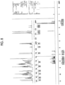
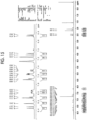
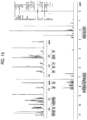
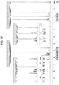
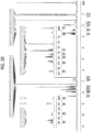
- Figs. 18 to 21 show 1 H NMR spectra (400 MHz, DMSO) of the compounds (D-22) and (D-24)-(D-26), respectively.
- the photoelectric conversion element of the form of Fig. 1 was produced using the obtained compound.
- the photoelectric conversion element includes a lower electrode 11, an electron blocking film 16A, a photoelectric conversion film 12, and an upper electrode 15.
- an amorphous ITO was formed into a film on the glass substrate by the sputtering method to form the lower electrode 11 (a thickness: 30 nm). Furthermore, the compound (EB-1) was formed into a film on the lower electrode 11 by the vacuum thermal vapor deposition method to form the electron blocking film 16A (a thickness: 30 nm).
- the compound (D-5) and the fullerene (C 60 ) were subjected to co-vapor deposition by the vacuum evaporation method so as to be respectively 100 nm in terms of single layer on the electron blocking film 16A to form a film in a state where the temperature of the substrate was controlled to 25°C, and the photoelectric conversion film 12 having the bulk hetero structure of 200 nm was formed.
- amorphous ITO was formed into a film on the photoelectric conversion film 12 by a sputtering method to form the upper electrode 15 (the transparent conductive film) (the thickness: 10 nm).
- the SiO film was formed as the sealing layer on the upper electrode 15 by a vacuum evaporation method
- an aluminum oxide (Al 2 O 3 ) layer was formed thereon by an atomic layer chemical vapor deposition (ALCVD) method to produce a photoelectric conversion element.
- ACVD atomic layer chemical vapor deposition
- the photoelectric conversion elements were produced using the compounds (D-6) to (D-32) and comparative compounds (R-1) to (R-6).
- the comparative compound (R-6) was thermally decomposed during vapor deposition and a photoelectric conversion element could not be produced.
- a voltage was applied to each of the photoelectric conversion elements manufactured in Examples and Comparative Examples so that the electric field strength was 1.0 ⁇ 10 5 V/cm.
- the photoelectric conversion efficiency of each photoelectric conversion element with respect to the photoelectric conversion element formed by using the compound (D-1) was evaluated as a relative value.
- the compound (D-5) and the fullerene (C 60 ) were subjected to co-vapor deposition by the vacuum thermal vapor deposition method so as to be respectively 100 nm in terms of single layer to form a film in a state where the temperature of the glass substrate was controlled to 25 °C, and the photoelectric conversion film having the bulk hetero structure of 200 nm was formed.
- the maximum absorption wavelength and absorption half-width of the photoelectric conversion film were measured using a spectrophotometer U3310 manufactured by Hitachi High-Tech Co., Ltd.
- the absorption half-width represents the difference between the two wavelengths at which the light absorbance at the maximum absorption wavelength was 0.5 times that of the maximum absorption wavelength (the point at which the light absorbance at 0.5 times the maximum absorption is at the maximum absorption wavelength was observed at two points on the long wavelength side and the short wavelength side).
- the absorption half-width is preferably "AA”, “A” or “B”, and more preferably “AA” or “A”.
- the compound (D-5) was changed to the compounds (D-6) to (D-32) and the comparative compounds (R-1) to (R-5), and the same evaluations as above were carried out.
- the half-width of the absorption peak of the photoelectric conversion film was narrow.
- the performance of the photoelectric conversion element according to the embodiment of the present invention is "A" or higher in all evaluation items of 5-7, 10, 17, 18, 22, 24-27, 30 and 31 (are)).
- the same imaging element as shown in Fig. 3 was produced using the compounds (D-5) to (D-31).
- the photoelectric conversion element functioning as a green photoelectric conversion element was produced by the method described above.
- the blue photoelectric conversion element and the red photoelectric conversion element were produced with reference to the description of JP-A-2005-303266 .
- the absorption peak of the photoelectric conversion film in the photoelectric conversion element according to the embodiment of the present invention has a narrow half-width, light was easily received by the blue photoelectric conversion element and the red photoelectric conversion element, and color separation performance was excellent.
Landscapes
- Chemical & Material Sciences (AREA)
- Organic Chemistry (AREA)
- Physics & Mathematics (AREA)
- Spectroscopy & Molecular Physics (AREA)
- Engineering & Computer Science (AREA)
- Materials Engineering (AREA)
- Electromagnetism (AREA)
- Light Receiving Elements (AREA)
- Solid State Image Pick-Up Elements (AREA)
- Heterocyclic Carbon Compounds Containing A Hetero Ring Having Oxygen Or Sulfur (AREA)
- Indole Compounds (AREA)
- Nitrogen Condensed Heterocyclic Rings (AREA)
- Plural Heterocyclic Compounds (AREA)
- Facsimile Heads (AREA)
- Transforming Light Signals Into Electric Signals (AREA)
Claims (9)
- Composé de formule (2b-1) ou (2b-2) :

 Rc3 est un cycle aromatique polycyclique facultativement substitué, ou un groupe de formule (4A) :
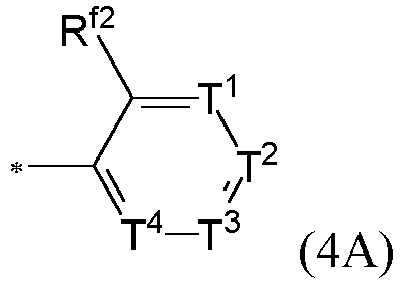 T1 à T4 sont chacun indépendamment N ou CRe12 dans lequel Re12 est chacun indépendamment H ou un substituant et, si une pluralité de Re12 sont présents, ils peuvent se lier l'un à l'autre pour former un cycle non-aromatique ne contenant aucune structure de cycle aromatique, etRf2 est un groupe alkyle, cyano, aryle facultativement substitué, ou hétéroaryle facultativement substitué ;R2, R3 sont chacun indépendamment un substituant, et R2 et R3 peuvent se lier l'un à l'autre pour former un cycle,Rs, R6 sont chacun indépendamment H ou un substituant,R11 à R24 sont chacun indépendamment H ou un substituant, et R11 à R16 et R17 à R24 peuvent se lier l'un à l'autre pour former un cycle non-aromatique ne contenant aucune structure de cycle aromatique ou un cycle fluorène,Rg1 à Rg4 sont chacun indépendamment H ou un substituant, et Rg1 à Rg4 peuvent se lier l'un à l'autre pour former un cycle,dans la formule (2b-1) le nombre total d'atomes de carbone contenus dans Rc3, R2, R3 et R11 à R16 est ≥ 5, etdans la formule (2b-2) le nombre total d'atomes de carbone contenus dans R2 et R3 est ≥ 4, et le nombre total d'atomes de carbone contenus dans Rc3, R2,R3 et R17 à R24 est ≥ 5.
 - Composé selon la revendication 1, dans lequel Rc3 est un groupe naphthyle facultativement substitué ou un groupe de formule (5A) ou (5B) :
 Re1 à Re4 sont chacun indépendamment H ou un substituant, Re1 à Re4 peuvent se lier l'un à l'autre pour former un cycle non-aromatique ne contenant aucune structure de cycle aromatique,Rf1 est un groupe alkyle, etRe5 à Re11, Re13 et Re14 sont chacun indépendamment H ou un substituant, et Re5 à Re11 et Re13 à Re14 peuvent se lier l'un à l'autre pour former un cycle.
 - Transducteur photo-électrique qui comprend (i) un film conducteur, (ii) un film de conversion photoélectrique, et (iii) un film conducteur transparent dans cet ordre ; dans lequel le film de conversion photoélectrique contient un composé de formule (2b-1) ou (2b-2) tel que défini selon la revendication 1 ou la revendication 2.
- Transducteur photo-électrique selon la revendication 3, dans lequel le film de conversion photoélectrique contient en outre un semiconducteur organique de type n, de préférence un semiconducteur organique de type n contenant des fullerènes choisis parmi un fullerène et un dérivé de celui-ci, et présente une hétérostructure massive formée dans un état où le composé de formule (2b-1) ou (2b-2) et le semiconducteur organique de type n sont mélangés.
- Transducteur photo-électrique selon la revendication 3 ou la revendication 4, comprenant en outre une ou plusieurs intercouches entre le film conducteur et le film conducteur transparent, en plus du film de conversion photoélectrique.
- Élément d'imagerie comprenant le transducteur photo-électrique selon l'une quelconque des revendications 3 à 5, et facultativement comprenant en outre un autre transducteur photo-électrique qui reçoit de la lumière présentant une longueur d'onde différente d'une longueur d'onde de lumière reçue par le transducteur photo-électrique.
- Élément d'imagerie selon la revendication 6, qui comprend en outre un autre transducteur photo-électrique, et dans lequel- le transducteur photo-électrique et l'autre transducteur photo-électrique sont laminés, et- au moins une partie du rayon d'incidence est transmise par le biais du transducteur photo-électrique, puis est reçue par l'autre transducteur photo-électrique.
- Élément d'imagerie selon la revendication 6 ou la revendication 7, dans lequel le transducteur photo-électrique est un transducteur photo-électrique vert et l'autre transducteur photo-électrique inclut un transducteur photo-électrique bleu et un transducteur photo-électrique rouge.
- Capteur optique comprenant le transducteur photo-électrique selon l'une quelconque des revendications 3 à 5.
Priority Applications (1)
| Application Number | Priority Date | Filing Date | Title |
|---|---|---|---|
| EP23162605.2A EP4227296A1 (fr) | 2018-03-28 | 2019-03-26 | Élément de conversion photoélectrique, élément d'imagerie, capteur optique et composé |
Applications Claiming Priority (3)
| Application Number | Priority Date | Filing Date | Title |
|---|---|---|---|
| JP2018062556 | 2018-03-28 | ||
| JP2018225658 | 2018-11-30 | ||
| PCT/JP2019/012786 WO2019189134A1 (fr) | 2018-03-28 | 2019-03-26 | Transducteur photo-électrique, élément d'imagerie, capteur optique, et composé |
Related Child Applications (2)
| Application Number | Title | Priority Date | Filing Date |
|---|---|---|---|
| EP23162605.2A Division-Into EP4227296A1 (fr) | 2018-03-28 | 2019-03-26 | Élément de conversion photoélectrique, élément d'imagerie, capteur optique et composé |
| EP23162605.2A Division EP4227296A1 (fr) | 2018-03-28 | 2019-03-26 | Élément de conversion photoélectrique, élément d'imagerie, capteur optique et composé |
Publications (3)
| Publication Number | Publication Date |
|---|---|
| EP3780127A1 EP3780127A1 (fr) | 2021-02-17 |
| EP3780127A4 EP3780127A4 (fr) | 2021-04-28 |
| EP3780127B1 true EP3780127B1 (fr) | 2024-09-18 |
Family
ID=68061650
Family Applications (2)
| Application Number | Title | Priority Date | Filing Date |
|---|---|---|---|
| EP19777795.6A Active EP3780127B1 (fr) | 2018-03-28 | 2019-03-26 | Transducteur photo-électrique, élément d'imagerie, capteur optique, et composé |
| EP23162605.2A Withdrawn EP4227296A1 (fr) | 2018-03-28 | 2019-03-26 | Élément de conversion photoélectrique, élément d'imagerie, capteur optique et composé |
Family Applications After (1)
| Application Number | Title | Priority Date | Filing Date |
|---|---|---|---|
| EP23162605.2A Withdrawn EP4227296A1 (fr) | 2018-03-28 | 2019-03-26 | Élément de conversion photoélectrique, élément d'imagerie, capteur optique et composé |
Country Status (7)
| Country | Link |
|---|---|
| US (1) | US11171165B2 (fr) |
| EP (2) | EP3780127B1 (fr) |
| JP (1) | JP7026780B2 (fr) |
| KR (1) | KR102342654B1 (fr) |
| CN (1) | CN111868951B (fr) |
| TW (1) | TWI823917B (fr) |
| WO (1) | WO2019189134A1 (fr) |
Families Citing this family (8)
| Publication number | Priority date | Publication date | Assignee | Title |
|---|---|---|---|---|
| CN113316572A (zh) * | 2019-04-26 | 2021-08-27 | 株式会社艾迪科 | 多次甲基化合物 |
| WO2021141078A1 (fr) * | 2020-01-10 | 2021-07-15 | 富士フイルム株式会社 | Élément de conversion photoélectrique, élément d'imagerie et capteur optique |
| CN116194444A (zh) * | 2020-07-17 | 2023-05-30 | 富士胶片株式会社 | 光电转换元件、成像元件、光传感器及化合物 |
| KR102857075B1 (ko) * | 2021-02-05 | 2025-09-08 | 후지필름 가부시키가이샤 | 광전 변환 소자, 촬상 소자, 광 센서, 화합물 |
| JP7725270B2 (ja) * | 2021-07-09 | 2025-08-19 | 富士フイルム株式会社 | 光電変換素子、撮像素子、光センサ、化合物 |
| JPWO2023054346A1 (fr) | 2021-09-29 | 2023-04-06 | ||
| CN117447384B (zh) * | 2023-10-24 | 2024-12-27 | 四川大学 | 一种螺杂环芳基类化合物及其应用 |
| WO2025142297A1 (fr) * | 2023-12-28 | 2025-07-03 | 富士フイルム株式会社 | Élément de conversion photoélectrique, élément d'imagerie, procédé de production d'élément d'imagerie, capteur optique et composé |
Citations (2)
| Publication number | Priority date | Publication date | Assignee | Title |
|---|---|---|---|---|
| US4705521A (en) * | 1986-08-22 | 1987-11-10 | Eastman Kodak Company | Process for reheating dye-receiving element containing stabilizer |
| US4757046A (en) * | 1986-10-06 | 1988-07-12 | Eastman Kodak Company | Merocyanine dye-donor element used in thermal dye transfer |
Family Cites Families (22)
| Publication number | Priority date | Publication date | Assignee | Title |
|---|---|---|---|---|
| JPS531250A (en) | 1976-06-28 | 1978-01-09 | Aoyoshi Seisakushiyo Kk | Method of producing synthetic resin shank and mold therefor |
| FR2577934B1 (fr) * | 1985-02-26 | 1988-01-08 | Saint Gobain Vitrage | Couche adhesive a base de polyurethane et son utilisation dans les vitrages feuilletes |
| US5030708A (en) * | 1990-12-17 | 1991-07-09 | Eastman Kodak Company | Colored polyester compositions |
| JP2005303266A (ja) | 2004-03-19 | 2005-10-27 | Fuji Photo Film Co Ltd | 撮像素子、その電場印加方法および印加した素子 |
| JP4972288B2 (ja) | 2004-08-30 | 2012-07-11 | 富士フイルム株式会社 | 撮像素子 |
| JP2006086160A (ja) * | 2004-09-14 | 2006-03-30 | Fuji Photo Film Co Ltd | 光電変換膜、光電変換素子、及び撮像素子、並びに、これらに電場を印加する方法 |
| TWI334232B (en) | 2005-10-13 | 2010-12-01 | Tube Smith Technology Co Ltd | Blue-laser-adsorbing material |
| JP4914597B2 (ja) | 2005-10-31 | 2012-04-11 | 富士フイルム株式会社 | 光電変換素子及び撮像素子、並びに、これらに電場を印加する方法 |
| JP2009135318A (ja) | 2007-11-30 | 2009-06-18 | Fujifilm Corp | 光電変換素子、撮像素子及び光センサー |
| JP5337381B2 (ja) * | 2008-01-18 | 2013-11-06 | 富士フイルム株式会社 | メロシアニン色素及び光電変換素子 |
| US8847208B2 (en) | 2009-06-03 | 2014-09-30 | Fujifilm Corporation | Photoelectric conversion device and imaging device having decreased dark current |
| JP5557663B2 (ja) | 2009-09-11 | 2014-07-23 | 富士フイルム株式会社 | 光電変換素子及びその製造方法、光センサ、並びに撮像素子及びそれらの駆動方法 |
| CN102024907B (zh) | 2009-09-11 | 2016-03-09 | 富士胶片株式会社 | 光电转换装置,其制备方法,光传感器,成像装置及它们的驱动方法 |
| JP4825925B2 (ja) | 2010-03-31 | 2011-11-30 | 富士フイルム株式会社 | 光電変換素子及びその製造方法、光センサ、並びに撮像素子及びそれらの駆動方法 |
| JP2012077064A (ja) * | 2010-09-08 | 2012-04-19 | Fujifilm Corp | 光電変換材料、該材料を含む膜、光電変換素子、光電変換素子の製造方法、光電変換素子の使用方法、光センサ、撮像素子 |
| JP5323025B2 (ja) | 2010-10-26 | 2013-10-23 | 富士フイルム株式会社 | 固体撮像素子 |
| JP6047109B2 (ja) | 2014-02-14 | 2016-12-21 | 富士フイルム株式会社 | 光電変換素子、光センサおよび撮像素子 |
| JP6872317B2 (ja) | 2015-03-27 | 2021-05-19 | 東友ファインケム株式会社Dongwoo Fine−Chem Co., Ltd. | 着色硬化性樹脂組成物 |
| KR102903774B1 (ko) | 2015-05-29 | 2025-12-24 | 소니 세미컨덕터 솔루션즈 가부시키가이샤 | 광전변환 소자 및 고체 촬상 장치 |
| JP6618785B2 (ja) | 2015-10-15 | 2019-12-11 | 日本化薬株式会社 | 撮像素子用光電変換素子用材料及びそれを含む光電変換素子 |
| WO2017159025A1 (fr) | 2016-03-15 | 2017-09-21 | ソニー株式会社 | Élément de conversion photoélectrique et dispositif de prise d'image à semi-conducteurs |
| JP6739290B2 (ja) | 2016-07-07 | 2020-08-12 | 日本化薬株式会社 | 撮像素子用光電変換素子用材料及びそれを含む光電変換素子 |
-
2019
- 2019-03-26 CN CN201980020313.4A patent/CN111868951B/zh active Active
- 2019-03-26 WO PCT/JP2019/012786 patent/WO2019189134A1/fr not_active Ceased
- 2019-03-26 JP JP2020510882A patent/JP7026780B2/ja active Active
- 2019-03-26 EP EP19777795.6A patent/EP3780127B1/fr active Active
- 2019-03-26 KR KR1020207025670A patent/KR102342654B1/ko active Active
- 2019-03-26 EP EP23162605.2A patent/EP4227296A1/fr not_active Withdrawn
- 2019-03-28 TW TW108110815A patent/TWI823917B/zh active
-
2020
- 2020-09-08 US US17/015,067 patent/US11171165B2/en active Active
Patent Citations (2)
| Publication number | Priority date | Publication date | Assignee | Title |
|---|---|---|---|---|
| US4705521A (en) * | 1986-08-22 | 1987-11-10 | Eastman Kodak Company | Process for reheating dye-receiving element containing stabilizer |
| US4757046A (en) * | 1986-10-06 | 1988-07-12 | Eastman Kodak Company | Merocyanine dye-donor element used in thermal dye transfer |
Also Published As
| Publication number | Publication date |
|---|---|
| EP3780127A4 (fr) | 2021-04-28 |
| KR102342654B1 (ko) | 2021-12-23 |
| TWI823917B (zh) | 2023-12-01 |
| KR20200118153A (ko) | 2020-10-14 |
| EP4227296A1 (fr) | 2023-08-16 |
| CN111868951B (zh) | 2025-01-17 |
| EP3780127A1 (fr) | 2021-02-17 |
| TW201942107A (zh) | 2019-11-01 |
| JPWO2019189134A1 (ja) | 2021-03-18 |
| CN111868951A (zh) | 2020-10-30 |
| US11171165B2 (en) | 2021-11-09 |
| JP7026780B2 (ja) | 2022-02-28 |
| US20200411569A1 (en) | 2020-12-31 |
| WO2019189134A1 (fr) | 2019-10-03 |
Similar Documents
| Publication | Publication Date | Title |
|---|---|---|
| EP3780127B1 (fr) | Transducteur photo-électrique, élément d'imagerie, capteur optique, et composé | |
| US11201294B2 (en) | Photoelectric conversion element, optical sensor, imaging element, and compound | |
| US11785843B2 (en) | Photoelectric conversion element, optical sensor, and imaging element | |
| US10886479B2 (en) | Photoelectric conversion element, optical sensor, imaging element, and compound | |
| US20230232713A1 (en) | Photoelectric conversion element, imaging element, optical sensor, and compound | |
| US12268092B2 (en) | Photoelectric conversion element, imaging element, optical sensor, material for photoelectric conversion element, and compound | |
| EP4290596A1 (fr) | Élément de conversion photoélectrique, élément d'imagerie, photocapteur et composé | |
| US20190140189A1 (en) | Photoelectric conversion element, imaging element, optical sensor, and compound | |
| US20210135121A1 (en) | Photoelectric conversion element, imaging element, optical sensor, and compound | |
| KR20190062531A (ko) | 광전 변환 소자, 광 센서 및 촬상 소자 | |
| US20190157350A1 (en) | Photoelectric conversion element, imaging element, optical sensor, and compound | |
| US20220109117A1 (en) | Photoelectric conversion element, imaging element, optical sensor, and material for photoelectric conversion element | |
| JP7133707B2 (ja) | 光電変換素子、撮像素子、光センサ、光電変換素子用材料、撮像素子用材料、光センサ用材料 | |
| JP7382404B2 (ja) | 光電変換素子、撮像素子、光センサ、光電変換素子用材料 | |
| JP7215970B2 (ja) | 光電変換素子、撮像素子、光センサ、光電変換素子用材料、化合物 | |
| EP3805241A1 (fr) | Composé et dispositif photoélectrique, capteur d'image et dispositif électronique le comprenant |
Legal Events
| Date | Code | Title | Description |
|---|---|---|---|
| STAA | Information on the status of an ep patent application or granted ep patent |
Free format text: STATUS: THE INTERNATIONAL PUBLICATION HAS BEEN MADE |
|
| PUAI | Public reference made under article 153(3) epc to a published international application that has entered the european phase |
Free format text: ORIGINAL CODE: 0009012 |
|
| STAA | Information on the status of an ep patent application or granted ep patent |
Free format text: STATUS: REQUEST FOR EXAMINATION WAS MADE |
|
| 17P | Request for examination filed |
Effective date: 20200921 |
|
| AK | Designated contracting states |
Kind code of ref document: A1 Designated state(s): AL AT BE BG CH CY CZ DE DK EE ES FI FR GB GR HR HU IE IS IT LI LT LU LV MC MK MT NL NO PL PT RO RS SE SI SK SM TR |
|
| AX | Request for extension of the european patent |
Extension state: BA ME |
|
| RAP3 | Party data changed (applicant data changed or rights of an application transferred) |
Owner name: FUJIFILM CORPORATION |
|
| A4 | Supplementary search report drawn up and despatched |
Effective date: 20210326 |
|
| DAV | Request for validation of the european patent (deleted) | ||
| DAX | Request for extension of the european patent (deleted) | ||
| STAA | Information on the status of an ep patent application or granted ep patent |
Free format text: STATUS: EXAMINATION IS IN PROGRESS |
|
| 17Q | First examination report despatched |
Effective date: 20221118 |
|
| REG | Reference to a national code |
Ref country code: DE Ref country code: DE Ref legal event code: R079 Ref document number: 602019059127 Country of ref document: DE Free format text: PREVIOUS MAIN CLASS: H01L0051420000 Ipc: C07D0209120000 |
|
| RIC1 | Information provided on ipc code assigned before grant |
Ipc: C07D 495/14 20060101ALI20231219BHEP Ipc: C07D 495/10 20060101ALI20231219BHEP Ipc: C07D 487/04 20060101ALI20231219BHEP Ipc: C07D 513/04 20060101ALI20231219BHEP Ipc: C07D 498/04 20060101ALI20231219BHEP Ipc: C07D 495/04 20060101ALI20231219BHEP Ipc: C07D 491/153 20060101ALI20231219BHEP Ipc: C07D 491/14 20060101ALI20231219BHEP Ipc: C07D 491/048 20060101ALI20231219BHEP Ipc: C07D 471/04 20060101ALI20231219BHEP Ipc: C07D 413/06 20060101ALI20231219BHEP Ipc: C07D 409/06 20060101ALI20231219BHEP Ipc: C07D 405/06 20060101ALI20231219BHEP Ipc: H01L 27/146 20060101ALI20231219BHEP Ipc: C07D 417/06 20060101ALI20231219BHEP Ipc: C07D 403/06 20060101ALI20231219BHEP Ipc: C07D 401/06 20060101ALI20231219BHEP Ipc: C07D 209/96 20060101ALI20231219BHEP Ipc: C07D 209/60 20060101ALI20231219BHEP Ipc: C07D 209/12 20060101AFI20231219BHEP |
|
| GRAP | Despatch of communication of intention to grant a patent |
Free format text: ORIGINAL CODE: EPIDOSNIGR1 |
|
| STAA | Information on the status of an ep patent application or granted ep patent |
Free format text: STATUS: GRANT OF PATENT IS INTENDED |
|
| INTG | Intention to grant announced |
Effective date: 20240201 |
|
| GRAJ | Information related to disapproval of communication of intention to grant by the applicant or resumption of examination proceedings by the epo deleted |
Free format text: ORIGINAL CODE: EPIDOSDIGR1 |
|
| STAA | Information on the status of an ep patent application or granted ep patent |
Free format text: STATUS: EXAMINATION IS IN PROGRESS |
|
| INTC | Intention to grant announced (deleted) | ||
| GRAP | Despatch of communication of intention to grant a patent |
Free format text: ORIGINAL CODE: EPIDOSNIGR1 |
|
| STAA | Information on the status of an ep patent application or granted ep patent |
Free format text: STATUS: GRANT OF PATENT IS INTENDED |
|
| INTG | Intention to grant announced |
Effective date: 20240711 |
|
| GRAS | Grant fee paid |
Free format text: ORIGINAL CODE: EPIDOSNIGR3 |
|
| GRAA | (expected) grant |
Free format text: ORIGINAL CODE: 0009210 |
|
| STAA | Information on the status of an ep patent application or granted ep patent |
Free format text: STATUS: THE PATENT HAS BEEN GRANTED |
|
| AK | Designated contracting states |
Kind code of ref document: B1 Designated state(s): AL AT BE BG CH CY CZ DE DK EE ES FI FR GB GR HR HU IE IS IT LI LT LU LV MC MK MT NL NO PL PT RO RS SE SI SK SM TR |
|
| REG | Reference to a national code |
Ref country code: GB Ref legal event code: FG4D |
|
| REG | Reference to a national code |
Ref country code: CH Ref legal event code: EP |
|
| REG | Reference to a national code |
Ref country code: IE Ref legal event code: FG4D |
|
| REG | Reference to a national code |
Ref country code: DE Ref legal event code: R096 Ref document number: 602019059127 Country of ref document: DE |
|
| REG | Reference to a national code |
Ref country code: LT Ref legal event code: MG9D |
|
| PG25 | Lapsed in a contracting state [announced via postgrant information from national office to epo] |
Ref country code: NO Free format text: LAPSE BECAUSE OF FAILURE TO SUBMIT A TRANSLATION OF THE DESCRIPTION OR TO PAY THE FEE WITHIN THE PRESCRIBED TIME-LIMIT Effective date: 20241218 |
|
| PG25 | Lapsed in a contracting state [announced via postgrant information from national office to epo] |
Ref country code: GR Free format text: LAPSE BECAUSE OF FAILURE TO SUBMIT A TRANSLATION OF THE DESCRIPTION OR TO PAY THE FEE WITHIN THE PRESCRIBED TIME-LIMIT Effective date: 20241219 Ref country code: FI Free format text: LAPSE BECAUSE OF FAILURE TO SUBMIT A TRANSLATION OF THE DESCRIPTION OR TO PAY THE FEE WITHIN THE PRESCRIBED TIME-LIMIT Effective date: 20240918 |
|
| PG25 | Lapsed in a contracting state [announced via postgrant information from national office to epo] |
Ref country code: BG Free format text: LAPSE BECAUSE OF FAILURE TO SUBMIT A TRANSLATION OF THE DESCRIPTION OR TO PAY THE FEE WITHIN THE PRESCRIBED TIME-LIMIT Effective date: 20240918 |
|
| PG25 | Lapsed in a contracting state [announced via postgrant information from national office to epo] |
Ref country code: LV Free format text: LAPSE BECAUSE OF FAILURE TO SUBMIT A TRANSLATION OF THE DESCRIPTION OR TO PAY THE FEE WITHIN THE PRESCRIBED TIME-LIMIT Effective date: 20240918 |
|
| PG25 | Lapsed in a contracting state [announced via postgrant information from national office to epo] |
Ref country code: HR Free format text: LAPSE BECAUSE OF FAILURE TO SUBMIT A TRANSLATION OF THE DESCRIPTION OR TO PAY THE FEE WITHIN THE PRESCRIBED TIME-LIMIT Effective date: 20240918 |
|
| REG | Reference to a national code |
Ref country code: NL Ref legal event code: MP Effective date: 20240918 |
|
| PG25 | Lapsed in a contracting state [announced via postgrant information from national office to epo] |
Ref country code: RS Free format text: LAPSE BECAUSE OF FAILURE TO SUBMIT A TRANSLATION OF THE DESCRIPTION OR TO PAY THE FEE WITHIN THE PRESCRIBED TIME-LIMIT Effective date: 20241218 |
|
| PG25 | Lapsed in a contracting state [announced via postgrant information from national office to epo] |
Ref country code: RS Free format text: LAPSE BECAUSE OF FAILURE TO SUBMIT A TRANSLATION OF THE DESCRIPTION OR TO PAY THE FEE WITHIN THE PRESCRIBED TIME-LIMIT Effective date: 20241218 Ref country code: NO Free format text: LAPSE BECAUSE OF FAILURE TO SUBMIT A TRANSLATION OF THE DESCRIPTION OR TO PAY THE FEE WITHIN THE PRESCRIBED TIME-LIMIT Effective date: 20241218 Ref country code: LV Free format text: LAPSE BECAUSE OF FAILURE TO SUBMIT A TRANSLATION OF THE DESCRIPTION OR TO PAY THE FEE WITHIN THE PRESCRIBED TIME-LIMIT Effective date: 20240918 Ref country code: HR Free format text: LAPSE BECAUSE OF FAILURE TO SUBMIT A TRANSLATION OF THE DESCRIPTION OR TO PAY THE FEE WITHIN THE PRESCRIBED TIME-LIMIT Effective date: 20240918 Ref country code: GR Free format text: LAPSE BECAUSE OF FAILURE TO SUBMIT A TRANSLATION OF THE DESCRIPTION OR TO PAY THE FEE WITHIN THE PRESCRIBED TIME-LIMIT Effective date: 20241219 Ref country code: FI Free format text: LAPSE BECAUSE OF FAILURE TO SUBMIT A TRANSLATION OF THE DESCRIPTION OR TO PAY THE FEE WITHIN THE PRESCRIBED TIME-LIMIT Effective date: 20240918 Ref country code: BG Free format text: LAPSE BECAUSE OF FAILURE TO SUBMIT A TRANSLATION OF THE DESCRIPTION OR TO PAY THE FEE WITHIN THE PRESCRIBED TIME-LIMIT Effective date: 20240918 |
|
| REG | Reference to a national code |
Ref country code: AT Ref legal event code: MK05 Ref document number: 1724605 Country of ref document: AT Kind code of ref document: T Effective date: 20240918 |
|
| PG25 | Lapsed in a contracting state [announced via postgrant information from national office to epo] |
Ref country code: NL Free format text: LAPSE BECAUSE OF FAILURE TO SUBMIT A TRANSLATION OF THE DESCRIPTION OR TO PAY THE FEE WITHIN THE PRESCRIBED TIME-LIMIT Effective date: 20240918 |
|
| PG25 | Lapsed in a contracting state [announced via postgrant information from national office to epo] |
Ref country code: PT Free format text: LAPSE BECAUSE OF FAILURE TO SUBMIT A TRANSLATION OF THE DESCRIPTION OR TO PAY THE FEE WITHIN THE PRESCRIBED TIME-LIMIT Effective date: 20250120 Ref country code: IS Free format text: LAPSE BECAUSE OF FAILURE TO SUBMIT A TRANSLATION OF THE DESCRIPTION OR TO PAY THE FEE WITHIN THE PRESCRIBED TIME-LIMIT Effective date: 20250118 |
|
| PG25 | Lapsed in a contracting state [announced via postgrant information from national office to epo] |
Ref country code: RO Free format text: LAPSE BECAUSE OF FAILURE TO SUBMIT A TRANSLATION OF THE DESCRIPTION OR TO PAY THE FEE WITHIN THE PRESCRIBED TIME-LIMIT Effective date: 20240918 Ref country code: SM Free format text: LAPSE BECAUSE OF FAILURE TO SUBMIT A TRANSLATION OF THE DESCRIPTION OR TO PAY THE FEE WITHIN THE PRESCRIBED TIME-LIMIT Effective date: 20240918 |
|
| PG25 | Lapsed in a contracting state [announced via postgrant information from national office to epo] |
Ref country code: ES Free format text: LAPSE BECAUSE OF FAILURE TO SUBMIT A TRANSLATION OF THE DESCRIPTION OR TO PAY THE FEE WITHIN THE PRESCRIBED TIME-LIMIT Effective date: 20240918 |
|
| PG25 | Lapsed in a contracting state [announced via postgrant information from national office to epo] |
Ref country code: EE Free format text: LAPSE BECAUSE OF FAILURE TO SUBMIT A TRANSLATION OF THE DESCRIPTION OR TO PAY THE FEE WITHIN THE PRESCRIBED TIME-LIMIT Effective date: 20240918 Ref country code: AT Free format text: LAPSE BECAUSE OF FAILURE TO SUBMIT A TRANSLATION OF THE DESCRIPTION OR TO PAY THE FEE WITHIN THE PRESCRIBED TIME-LIMIT Effective date: 20240918 |
|
| PG25 | Lapsed in a contracting state [announced via postgrant information from national office to epo] |
Ref country code: CZ Free format text: LAPSE BECAUSE OF FAILURE TO SUBMIT A TRANSLATION OF THE DESCRIPTION OR TO PAY THE FEE WITHIN THE PRESCRIBED TIME-LIMIT Effective date: 20240918 Ref country code: PL Free format text: LAPSE BECAUSE OF FAILURE TO SUBMIT A TRANSLATION OF THE DESCRIPTION OR TO PAY THE FEE WITHIN THE PRESCRIBED TIME-LIMIT Effective date: 20240918 |
|
| PG25 | Lapsed in a contracting state [announced via postgrant information from national office to epo] |
Ref country code: IT Free format text: LAPSE BECAUSE OF FAILURE TO SUBMIT A TRANSLATION OF THE DESCRIPTION OR TO PAY THE FEE WITHIN THE PRESCRIBED TIME-LIMIT Effective date: 20240918 Ref country code: SK Free format text: LAPSE BECAUSE OF FAILURE TO SUBMIT A TRANSLATION OF THE DESCRIPTION OR TO PAY THE FEE WITHIN THE PRESCRIBED TIME-LIMIT Effective date: 20240918 |
|
| REG | Reference to a national code |
Ref country code: DE Ref legal event code: R097 Ref document number: 602019059127 Country of ref document: DE |
|
| PG25 | Lapsed in a contracting state [announced via postgrant information from national office to epo] |
Ref country code: DK Free format text: LAPSE BECAUSE OF FAILURE TO SUBMIT A TRANSLATION OF THE DESCRIPTION OR TO PAY THE FEE WITHIN THE PRESCRIBED TIME-LIMIT Effective date: 20240918 |
|
| PLBE | No opposition filed within time limit |
Free format text: ORIGINAL CODE: 0009261 |
|
| STAA | Information on the status of an ep patent application or granted ep patent |
Free format text: STATUS: NO OPPOSITION FILED WITHIN TIME LIMIT |
|
| 26N | No opposition filed |
Effective date: 20250619 |
|
| PG25 | Lapsed in a contracting state [announced via postgrant information from national office to epo] |
Ref country code: SE Free format text: LAPSE BECAUSE OF FAILURE TO SUBMIT A TRANSLATION OF THE DESCRIPTION OR TO PAY THE FEE WITHIN THE PRESCRIBED TIME-LIMIT Effective date: 20240918 |
|
| PG25 | Lapsed in a contracting state [announced via postgrant information from national office to epo] |
Ref country code: MC Free format text: LAPSE BECAUSE OF FAILURE TO SUBMIT A TRANSLATION OF THE DESCRIPTION OR TO PAY THE FEE WITHIN THE PRESCRIBED TIME-LIMIT Effective date: 20240918 |
|
| REG | Reference to a national code |
Ref country code: CH Ref legal event code: H13 Free format text: ST27 STATUS EVENT CODE: U-0-0-H10-H13 (AS PROVIDED BY THE NATIONAL OFFICE) Effective date: 20251023 |
|
| PG25 | Lapsed in a contracting state [announced via postgrant information from national office to epo] |
Ref country code: LU Free format text: LAPSE BECAUSE OF NON-PAYMENT OF DUE FEES Effective date: 20250326 |
|
| GBPC | Gb: european patent ceased through non-payment of renewal fee |
Effective date: 20250326 |
|
| REG | Reference to a national code |
Ref country code: BE Ref legal event code: MM Effective date: 20250331 |
|
| PG25 | Lapsed in a contracting state [announced via postgrant information from national office to epo] |
Ref country code: GB Free format text: LAPSE BECAUSE OF NON-PAYMENT OF DUE FEES Effective date: 20250326 |
|
| PG25 | Lapsed in a contracting state [announced via postgrant information from national office to epo] |
Ref country code: FR Free format text: LAPSE BECAUSE OF NON-PAYMENT OF DUE FEES Effective date: 20250331 |
|
| PG25 | Lapsed in a contracting state [announced via postgrant information from national office to epo] |
Ref country code: BE Free format text: LAPSE BECAUSE OF NON-PAYMENT OF DUE FEES Effective date: 20250331 |
|
| PG25 | Lapsed in a contracting state [announced via postgrant information from national office to epo] |
Ref country code: CH Free format text: LAPSE BECAUSE OF NON-PAYMENT OF DUE FEES Effective date: 20250331 |
|
| PG25 | Lapsed in a contracting state [announced via postgrant information from national office to epo] |
Ref country code: IE Free format text: LAPSE BECAUSE OF NON-PAYMENT OF DUE FEES Effective date: 20250326 |
|
| PGFP | Annual fee paid to national office [announced via postgrant information from national office to epo] |
Ref country code: DE Payment date: 20260128 Year of fee payment: 8 |