EP3784006A1 - Beleuchtungsvorrichtung - Google Patents
Beleuchtungsvorrichtung Download PDFInfo
- Publication number
- EP3784006A1 EP3784006A1 EP20161771.9A EP20161771A EP3784006A1 EP 3784006 A1 EP3784006 A1 EP 3784006A1 EP 20161771 A EP20161771 A EP 20161771A EP 3784006 A1 EP3784006 A1 EP 3784006A1
- Authority
- EP
- European Patent Office
- Prior art keywords
- light
- light source
- voltage divider
- source
- lighting apparatus
- Prior art date
- Legal status (The legal status is an assumption and is not a legal conclusion. Google has not performed a legal analysis and makes no representation as to the accuracy of the status listed.)
- Granted
Links
Images

Classifications
-
- H—ELECTRICITY
- H05—ELECTRIC TECHNIQUES NOT OTHERWISE PROVIDED FOR
- H05B—ELECTRIC HEATING; ELECTRIC LIGHT SOURCES NOT OTHERWISE PROVIDED FOR; CIRCUIT ARRANGEMENTS FOR ELECTRIC LIGHT SOURCES, IN GENERAL
- H05B45/00—Circuit arrangements for operating light-emitting diodes [LED]
- H05B45/30—Driver circuits
- H05B45/37—Converter circuits
-
- H—ELECTRICITY
- H05—ELECTRIC TECHNIQUES NOT OTHERWISE PROVIDED FOR
- H05B—ELECTRIC HEATING; ELECTRIC LIGHT SOURCES NOT OTHERWISE PROVIDED FOR; CIRCUIT ARRANGEMENTS FOR ELECTRIC LIGHT SOURCES, IN GENERAL
- H05B45/00—Circuit arrangements for operating light-emitting diodes [LED]
- H05B45/20—Controlling the colour of the light
-
- H—ELECTRICITY
- H05—ELECTRIC TECHNIQUES NOT OTHERWISE PROVIDED FOR
- H05B—ELECTRIC HEATING; ELECTRIC LIGHT SOURCES NOT OTHERWISE PROVIDED FOR; CIRCUIT ARRANGEMENTS FOR ELECTRIC LIGHT SOURCES, IN GENERAL
- H05B45/00—Circuit arrangements for operating light-emitting diodes [LED]
- H05B45/30—Driver circuits
- H05B45/357—Driver circuits specially adapted for retrofit LED light sources
- H05B45/3574—Emulating the electrical or functional characteristics of incandescent lamps
- H05B45/3577—Emulating the dimming characteristics, brightness or colour temperature of incandescent lamps
-
- H—ELECTRICITY
- H05—ELECTRIC TECHNIQUES NOT OTHERWISE PROVIDED FOR
- H05B—ELECTRIC HEATING; ELECTRIC LIGHT SOURCES NOT OTHERWISE PROVIDED FOR; CIRCUIT ARRANGEMENTS FOR ELECTRIC LIGHT SOURCES, IN GENERAL
- H05B45/00—Circuit arrangements for operating light-emitting diodes [LED]
- H05B45/40—Details of LED load circuits
- H05B45/44—Details of LED load circuits with an active control inside an LED matrix
- H05B45/46—Details of LED load circuits with an active control inside an LED matrix having LEDs disposed in parallel lines
Definitions
- the present application is related to a lighting apparatus and more particularly related to a lighting apparatus with desired color temperature.
- LED Light Emitted Diode
- More and more traditional lighting devices are replaced with LED lighting devices for LED having low cost and high optical efficiency.
- color temperature is playing a more and more important role.
- the color temperature of a LED lighting apparatus is preferred to be kept at a desired color temperature.
- the color temperature of a LED lighting apparatus is preferred to be adjusted dynamically by users with manual control or under automatic control.
- more than one types of LED devices may be used together to achieve a mixed optical parameter, e.g. color temperature.
- more than one control circuits need to be prepared for each type of LED devices. But, such design usually involves higher cost and may cause some instable light output.
- a lighting apparatus includes a first light source, a second light source, a current source, a pulse width modulation (PWM) circuit for generating a PWM signal and a switch circuit.
- PWM pulse width modulation
- the first light source emits a first light with a first optical parameter.
- the second light source emits a second light with a second optical parameter.
- the first optical parameter and the second optical parameter comprise color temperature and/or light spectrum distribution, e.g. different strengths on different frequency segments.
- the first light source and the second light source may each include one more than one LED modules. To emit different color temperatures, different fluorescent layers may be disposed upon LED chips for generating different color temperatures.
- the current source generates a driving current.
- the current source may be various constant current circuits that may convert DC (Direct Current) or AC (Alternating Current) to a suitable driving current for driving LED modules to emit light.
- the pulse width modulation (PWM) circuit is used for generating a PWM signal.
- the switch circuit guides the driving current to either the first light source or the second light source by reference to the PWM signal so as by mixing the first light of the first optical parameter and the second light of the second optical parameter to obtain a desired mixed output light of a mixed optical parameter.
- the switch circuit when the PWM signal is at high level, guides the driving current to the first light source, and when the PWM signal is at low level, the switch circuit guides the driving current to the second light source.
- a PWM signal is a square wave that has consecutive high voltage levels and low voltage levels.
- the PWM signal is at high voltage level, e.g., the PWM signal being at high level, the driving current is directed to drive the first light source.
- the PWM signal is at low voltage level, e.g. the PWM signal being at low level, the driving current is directed to the second light source.
- the first optical parameter is a first color temperature and the second optical parameter is a second color temperature and a mixed color temperature of the mixed output light is adjusted by changing the PWM signal. For example, in a time period, the first light source is turned on for 70% of time while the second light source is turned on for 30% of time. In such case, the mixed color temperature appears to be 70% of the color temperature of the first light source plus 30% of the color temperature of the second light source.
- the first light source and the second light source do not receive the driving current at the same time. In other words, the first light source and second light source are controlled not to turn on at the same time according to the PWM signal.
- the first light source and the second light source are LED light sources.
- the PMW signal is also supplied to the current source for determining a current value of the driving current.
- the same PWM signal is used for adjusting or determining the mixed color temperature and also used for adjusting or determining the overall driving current, so as to adjust luminance level.
- the light apparatus also includes an AC/DC converter for converting an AC power source to a DC power source supplying to the current source for generating the driving current.
- the switch circuit includes a first switch unit connected in series with the first light source forming a first light path.
- a control gate of the first switch unit receives the PWM signal.
- the switch circuit also includes a second switch unit connected in series with the second light source forming a second light path. The second light path is connected with the first light path in parallel.
- a one-way conductive unit with a first terminal connected to a control gate of the second switch unit and a first output terminal of the current source.
- a second terminal of the one-way conductive unit is connected between the first switch unit and the first light source.
- the first switch unit and the second switch unit are transistors.
- the switch circuit further includes a first voltage divider.
- the first voltage divider includes a first voltage divider resistor and a second divider resistor connected with the first light path in parallel.
- the control gate of the first switch unit is connected between the first voltage divider resistor and the second voltage divider resistor.
- the switch circuit may further include a second voltage divider.
- the second voltage divider includes a fourth voltage divider resistor and a fifth voltage divider resistor.
- the second voltage divider is connected with the second light path in parallel.
- the control gate of the second switch unit is connected between the fourth voltage divider resistor and the fifth voltage divider resistor.
- the switch circuit may also include a third voltage divider.
- the third voltage divider includes a third voltage divider resistor.
- the third voltage divider resistor is connected between a second terminal of the one-way conductor and a second output terminal of the current source.
- the one-way conductor is a diode device.
- the first output terminal is a positive terminal of the current source, and the second output terminal is a negative terminal of the current source.
- the lighting apparatus may also include a tuner module connected to the current source for adjusting the driving current according to the PWM signal.
- the lighting apparatus may also further include a tuner module connected to the current source for adjusting the driving current by inputting a second PWM signal.
- a lighting apparatus includes a first light source 306, a second light source 305, a current source 302, a switch circuit 303 and a PWM (Pulse Width Modulation) circuit 304.
- a PWM Pulse Width Modulation
- the switch circuit 303 receives a PWM signal from the PWM circuit 304 and distributes a driving current in alternating order to either the first light source 306 or the second light source 305.
- a lighting apparatus includes a first light source, a second light source, a current source, a PWM (Pulse Width Modulation) circuit for generating a PWM signal and a switch circuit.
- PWM Pulse Width Modulation
- the first light source emits a first light with a first optical parameter.
- the second light source emits a second light with a second optical parameter.
- the first optical parameter and the second optical parameter comprise color temperature and/or light spectrum distribution, e.g., different strengths on different frequency segments.
- the first light source and the second light source may each include one more than one LED (Light Emitting Diode) modules. To emit different color temperatures, different fluorescent layers may be disposed upon LED chips for generating different color temperatures.
- the current source generates a driving current.
- the current source may be various constant current circuits that may convert DC (Direct Current) or AC (Alternating Current) to a suitable driving current for driving LED modules to emit light.
- the PWM circuit is used for generating a PWM signal.
- the switch circuit guides the driving current to either the first light source or the second light source by reference to the PWM signal so as by mixing the first light of the first optical parameter and the second light of the second optical parameter to obtain a desired mixed output light of a mixed optical parameter.
- the switch circuit when the PWM signal is at high level, guides the driving current to the first light source, and when the PWM signal is at low level, the switch circuit guides the driving current to the second light source.
- a PWM signal is a square wave that has consecutive high voltage levels and low voltage levels.
- the driving current is directed to drive the first light source.
- the PWM signal is at low voltage level, e.g. the PWM signal being at low level, the driving current is directed to the second light source.
- the first optical parameter is a first color temperature and the second optical parameter is a second color temperature and a mixed color temperature of the mixed output light is adjusted by changing the PWM signal. For example, in a time period, the first light source is turned on for 70% of time while the second light source is turned on for 30% of time. In such case, the mixed color temperature appears to be 70% of the color temperature of the first light source plus 30% of the color temperature of the second light source.
- the first light source and the second light source do not receive the driving current at the same time. In other words, the first light source and second light source are controlled not to turn on at the same time according to the PWM signal.
- the first light source and the second light source are LED light sources.
- the PMW signal is also supplied to the current source for determining a current value of the driving current.
- the same PWM signal is used for adjusting or determining the mixed color temperature and also used for adjusting or determining the overall driving current, so as to adjust luminance level.
- the light apparatus also includes an AC/DC converter for converting an AC power source to a DC power source supplying to the current source for generating the driving current.
- the switch circuit includes a first switch unit connected in series with the first light source forming a first light path.
- a control gate of the first switch unit receives the PWM signal.
- the switch circuit also includes a second switch unit connected in series with the second light source forming a second light path. The second light path is connected with the first light path in parallel.
- a one-way conductive unit with a first terminal connected to a control gate of the second switch unit and a first output terminal of the current source.
- a second terminal of the one-way conductive unit is connected between the first switch unit and the first light source.
- the first switch unit and the second switch unit are transistors.
- the switch circuit further includes a first voltage divider.
- the first voltage divider includes a first voltage divider resistor and a second divider resistor connected with the first light path in parallel.
- the control gate of the first switch unit is connected between the first voltage divider resistor and the second voltage divider resistor.
- the switch circuit may further include a second voltage divider.
- the second voltage divider includes a fourth voltage divider resistor and a fifth voltage divider resistor.
- the second voltage divider is connected with the second light path in parallel.
- the control gate of the second switch unit is connected between the fourth voltage divider resistor and the fifth voltage divider resistor.
- the switch circuit may also include a third voltage divider.
- the third voltage divider includes a third voltage divider resistor.
- the third voltage divider resistor is connected between a second terminal of the one-way conductor and a second output terminal of the current source.
- the one-way conductor is a diode device.
- the first output terminal is a positive terminal of the current source, and the second output terminal is a negative terminal of the current source.
- the lighting apparatus may also include a tuner module connected to the current source for adjusting the driving current according to the PWM signal.
- the lighting apparatus may also further include a tuner module connected to the current source for adjusting the driving current by inputting a second PWM signal.
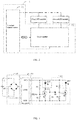
- Fig. 2 shows an embodiment.
- the embodiment illustrates a lighting apparatus with color temperature adjusting or determining function by mixing multiple LED modules with different color temperatures.
- the first light source may be selected with a warm color temperature while the second light source may be selected with a cold color temperature.
- the first light source may include more than one LED modules connected in series or in other combination manner.
- the second light source may include more than one LED modules connected in series or in other combination manner.
- the lighting apparatus includes a constant current source 11.
- the constant current source 11 receives a power input and converts the power input into a constant current supplying to two LED light sources.
- the switch module 12 includes a PWM signal input terminal for receiving a PWM signal from a PWM circuit as a color temperature control signal.
- the switch module 12 also includes two terminals respectively connected to a first LED module 171 and a second LED module 172 with different color temperatures.
- the constant current source 11 has its positive output terminals respectively connected to the first LED module 171 and the second LED module 172.
- the LED module 171 and the second LED module 172 then further connect to a negative output terminal of the constant current source 11 via the switch module 11.
- the switch module 12 uses its internal circuit to decode the PWM signal to control a first light path of the first LED module 171 and a second light path of the second LED module 172 to turn on and turn off in a corresponding on/off ratio to produce desired color temperature.
- the first LED module 171 when the PWM signal is at high voltage level, the first LED module 171 is turned on and the second LED module 172 is turned off.
- the PWM signal when the PWM signal is at low voltage level, the first LED module 171 is turned off and the second LED module 172 is turned on.
- Such design may avoid undesired blink while the current is kept constant and stable.
- only one PWM circuit is necessary and thus the overall cost is decreased at the same time.
- Fig. 3 a circuit diagram is provided to teach, not to limit the present application scope, persons of ordinary skilled in the art to enable the present application.
- the lighting apparatus in Fig. 3 includes a constant module 411.
- the constant current module 411 receives a power input and converts the power input to a constant current supplying to two LED modules.
- the constant current module 411 includes an AC/DC conversion module for converting an AC power input to a DC output.
- the switch module 412 controls turn-on and turn-off of the first LED module and the second LED module according to a PWM signal. In the same time, the switch module 412 keeps the sum of current used by the first LED module and the second LED module.
- the switch module 12 includes a first transistor Q1, a second transistor Q2 and a one-way conductor unit D1.
- the first transistor Q1 and the second transistor Q2 may be field effect transistors.
- the first transistor Q1 and the first LED module LED1 are connected in series forming a first light path.
- the control gate of the first transistor Q1 receives a PWM signal.
- the second transistor Q2 and the second LED module LED2 are connected in series forming a second light path.
- the second light path and the first light path are connected in parallel.
- the positive terminal of the one-way conductor unit D1 is connected to the control gate of the second transistor Q2 and the positive output OUT+ of the constant current module 411.
- the negative terminal of the one-way conductor unit D1 is connected between the first transistor Q1 and the first LED module LED module.
- the positive terminals of the two LED modules respectively connect to the positive output terminals OUT+.
- the negative terminals of the two LED modules are respectively connected to drain ends of the two transistors.
- the source ends of the transistors are respectively connected to the negative output terminal OUT- of the constant current module 411.
- the first transistor When the PWM signal is at high voltage level, the first transistor is turned on and the current of the constant current module is output via the terminal OUT+ to the first LED module LED1, the transistor Q1 and the terminal OUT-.
- the first transistor Q1 is turned on, the drain end of the first transistor Q1 is at low voltage level, which means the negative terminal of the one-way conductor unit D1 is at low voltage level. Because the one-way conductor unit Q1 only allows one-way connection, the positive terminal of the one-way conductor unit Q1 is also at low voltage level, which means the control gate of the second transistor Q2 being at low voltage level.
- the second transistor Q2 is turned off in such time.
- the second LED module LED2 is turned off and not emitting light.
- the first transistor Q1 When the PWM signal is at low voltage level, the first transistor Q1 is turned off.
- the first LED module LED1 is turned off. Because the first transistor Q1 is turned off, the drain end of the first transistor Q1 is at high voltage level, which means the negative terminal of the one-way conductor unit D1 is at high voltage level. Meanwhile, the positive terminal of the one-way conductor unit D1 is also at high voltage which is the same in the positive output terminal OUT+ of the constant current module 411.
- the control gate of the second transistor Q2 is at high voltage level and thus the second transistor Q2 is turned on and causes the second LED module LED2 to turn on.
- the driving current output by the constant current module 411 is either directed to the fist LED module LED1 or the second LED module LED2.
- the switch module 412 further includes a first voltage divider unit connected to the first light path in parallel.
- the first voltage divider unit includes a first voltage divider resistor R1 and a second voltage divider resistor R2.
- the control gate of the first transistor Q1 is connected between the first voltage divider resistor R1 and the second voltage resistor R2.
- the switch module 412 also includes a second voltage divider unit connected to the second light path in parallel.
- the second voltage divider includes a fourth voltage divider resistor R4 and a fifth voltage divider resistor R5.
- the control gate of the second transistor Q2 is connected between the fourth voltage divider resistor R4 and the fifth voltage divider resistor R5.
- the switch module 412 also includes a third voltage divider unit.
- the third voltage divider unit includes a third voltage divider resistor R3.
- the third voltage divider is connected between the negative terminal of the one-way conductor unit D1 and the negative terminal OUT- of the constant current module 411.
- the one-way conductor unit D1 is a diode device.
- the lighting apparatus may include a rectifier like a bridge module.
Landscapes
- Circuit Arrangement For Electric Light Sources In General (AREA)
Applications Claiming Priority (1)
| Application Number | Priority Date | Filing Date | Title |
|---|---|---|---|
| US16/546,162 US10772175B1 (en) | 2019-08-20 | 2019-08-20 | Lighting apparatus |
Publications (2)
| Publication Number | Publication Date |
|---|---|
| EP3784006A1 true EP3784006A1 (de) | 2021-02-24 |
| EP3784006B1 EP3784006B1 (de) | 2024-07-24 |
Family
ID=69784145
Family Applications (1)
| Application Number | Title | Priority Date | Filing Date |
|---|---|---|---|
| EP20161771.9A Active EP3784006B1 (de) | 2019-08-20 | 2020-03-09 | Beleuchtungsvorrichtung |
Country Status (2)
| Country | Link |
|---|---|
| US (1) | US10772175B1 (de) |
| EP (1) | EP3784006B1 (de) |
Families Citing this family (3)
| Publication number | Priority date | Publication date | Assignee | Title |
|---|---|---|---|---|
| CN207720473U (zh) * | 2017-12-15 | 2018-08-10 | 漳州立达信灯具有限公司 | 多档色温切换led电路 |
| JP2024125101A (ja) * | 2023-03-03 | 2024-09-13 | ラピステクノロジー株式会社 | ドライバ回路 |
| CN221354542U (zh) * | 2023-12-07 | 2024-07-16 | 江门市江海区和成照明有限公司 | 一种色温控制电路 |
Citations (3)
| Publication number | Priority date | Publication date | Assignee | Title |
|---|---|---|---|---|
| US20130043801A1 (en) * | 2011-08-19 | 2013-02-21 | Chao-Li Kuwu | Lighting device |
| US20150373790A1 (en) * | 2014-06-19 | 2015-12-24 | Nxp B.V. | Circuit and lighting unit for dimmable lighting applications |
| US10314124B1 (en) * | 2018-05-21 | 2019-06-04 | Shenzhen Longood Intelligent Electric Co., Ltd | LED driving power supply based on 2.4G remote controlling adjustment of brightness and color temperature |
Family Cites Families (11)
| Publication number | Priority date | Publication date | Assignee | Title |
|---|---|---|---|---|
| US20060237636A1 (en) * | 2003-06-23 | 2006-10-26 | Advanced Optical Technologies, Llc | Integrating chamber LED lighting with pulse amplitude modulation to set color and/or intensity of output |
| US9781793B2 (en) * | 2008-12-12 | 2017-10-03 | 02Micro, Inc. | Controlling brightness and color temperature of light sources |
| EP2671016B1 (de) * | 2011-02-04 | 2016-04-20 | Koninklijke Philips N.V. | Beleuchtungseinheit mit led-streifen |
| US20130229120A1 (en) * | 2012-03-05 | 2013-09-05 | Luxera, Inc. | Solid State Lighting System, Apparatus and Method with Flicker Removal |
| US8829800B2 (en) * | 2012-09-07 | 2014-09-09 | Cree, Inc. | Lighting component with independent DC-DC converters |
| US9844113B2 (en) * | 2013-01-25 | 2017-12-12 | Dialog Semiconductor Inc. | Adjusting color temperature in a dimmable LED lighting system |
| JP2015056377A (ja) * | 2013-09-13 | 2015-03-23 | パナソニックIpマネジメント株式会社 | 照明用光源及び照明装置 |
| JP6145821B2 (ja) * | 2013-09-13 | 2017-06-14 | パナソニックIpマネジメント株式会社 | 照明用光源及び照明装置 |
| US9618162B2 (en) * | 2014-04-25 | 2017-04-11 | Cree, Inc. | LED lamp |
| ES2908577T3 (es) * | 2016-04-22 | 2022-05-03 | Signify Holding Bv | Un procedimiento de control de una disposición de iluminación y un circuito de control de iluminación |
| CN207720473U (zh) * | 2017-12-15 | 2018-08-10 | 漳州立达信灯具有限公司 | 多档色温切换led电路 |
-
2019
- 2019-08-20 US US16/546,162 patent/US10772175B1/en active Active
-
2020
- 2020-03-09 EP EP20161771.9A patent/EP3784006B1/de active Active
Patent Citations (3)
| Publication number | Priority date | Publication date | Assignee | Title |
|---|---|---|---|---|
| US20130043801A1 (en) * | 2011-08-19 | 2013-02-21 | Chao-Li Kuwu | Lighting device |
| US20150373790A1 (en) * | 2014-06-19 | 2015-12-24 | Nxp B.V. | Circuit and lighting unit for dimmable lighting applications |
| US10314124B1 (en) * | 2018-05-21 | 2019-06-04 | Shenzhen Longood Intelligent Electric Co., Ltd | LED driving power supply based on 2.4G remote controlling adjustment of brightness and color temperature |
Also Published As
| Publication number | Publication date |
|---|---|
| US10772175B1 (en) | 2020-09-08 |
| EP3784006B1 (de) | 2024-07-24 |
Similar Documents
| Publication | Publication Date | Title |
|---|---|---|
| US8183795B2 (en) | LED current-supplying circuit and LED current-controlling circuit | |
| EP1860922B1 (de) | Verfahren und Vorrichtung zur Stromversorgung lichtemittierender Dioden-Arrays | |
| US8471483B2 (en) | Multi-channel LED driving system | |
| US9560704B2 (en) | LED driving device and LED lighting apparatus | |
| US8106596B2 (en) | Light source driving circuit | |
| US8269432B2 (en) | Offline LED lighting circuit with dimming control | |
| US9295119B2 (en) | Lighting device and illumination apparatus using the same | |
| EP3784006A1 (de) | Beleuchtungsvorrichtung | |
| WO2020037807A1 (zh) | 可调光照明装置及调光电路 | |
| JP2014176295A (ja) | 照明装置 | |
| US20110043510A1 (en) | Power supply for liquid crystal display | |
| US8247996B2 (en) | Backlight driving system utilizing one PWM controller to control two backlight units separately | |
| WO2016131558A1 (en) | Color-tunable led module with anti-parallel led strings | |
| CN103379706B (zh) | 驱动电路 | |
| CN212970164U (zh) | 一种基于0-10v调光器的调光调色电路及照明灯具 | |
| CN217904696U (zh) | 用于照明组件的调光电路以及照明组件 | |
| CN106982492B (zh) | 一种具有过载保护电路的调光器 | |
| JP7638198B2 (ja) | 照明装置、照明装置の駆動方法、車両用灯具 | |
| KR20160041290A (ko) | 색온도 제어 기능을 가지는 조명 장치 | |
| TW202021423A (zh) | Led背光驅動雙控制器級聯的系統和方法 | |
| KR20150076831A (ko) | 발광 다이오드 구동 장치 | |
| KR101961850B1 (ko) | LED(Light Emitting Diode) 조명 제어 장치 | |
| CN113068287B (zh) | 具有稳定输出电压的调光电路 | |
| CN223053139U (zh) | 一种推拔开关兼容通断控制led调色电路及照明装置 | |
| US8604720B2 (en) | Light emitting diode driving method |
Legal Events
| Date | Code | Title | Description |
|---|---|---|---|
| PUAI | Public reference made under article 153(3) epc to a published international application that has entered the european phase |
Free format text: ORIGINAL CODE: 0009012 |
|
| STAA | Information on the status of an ep patent application or granted ep patent |
Free format text: STATUS: REQUEST FOR EXAMINATION WAS MADE |
|
| 17P | Request for examination filed |
Effective date: 20200309 |
|
| AK | Designated contracting states |
Kind code of ref document: A1 Designated state(s): AL AT BE BG CH CY CZ DE DK EE ES FI FR GB GR HR HU IE IS IT LI LT LU LV MC MK MT NL NO PL PT RO RS SE SI SK SM TR |
|
| AX | Request for extension of the european patent |
Extension state: BA ME |
|
| STAA | Information on the status of an ep patent application or granted ep patent |
Free format text: STATUS: EXAMINATION IS IN PROGRESS |
|
| 17Q | First examination report despatched |
Effective date: 20221110 |
|
| GRAP | Despatch of communication of intention to grant a patent |
Free format text: ORIGINAL CODE: EPIDOSNIGR1 |
|
| STAA | Information on the status of an ep patent application or granted ep patent |
Free format text: STATUS: GRANT OF PATENT IS INTENDED |
|
| RIC1 | Information provided on ipc code assigned before grant |
Ipc: H05B 45/3577 20200101ALI20240417BHEP Ipc: H05B 45/46 20200101ALI20240417BHEP Ipc: H05B 45/20 20200101AFI20240417BHEP |
|
| INTG | Intention to grant announced |
Effective date: 20240507 |
|
| GRAS | Grant fee paid |
Free format text: ORIGINAL CODE: EPIDOSNIGR3 |
|
| GRAA | (expected) grant |
Free format text: ORIGINAL CODE: 0009210 |
|
| STAA | Information on the status of an ep patent application or granted ep patent |
Free format text: STATUS: THE PATENT HAS BEEN GRANTED |
|
| AK | Designated contracting states |
Kind code of ref document: B1 Designated state(s): AL AT BE BG CH CY CZ DE DK EE ES FI FR GB GR HR HU IE IS IT LI LT LU LV MC MK MT NL NO PL PT RO RS SE SI SK SM TR |
|
| REG | Reference to a national code |
Ref country code: GB Ref legal event code: FG4D |
|
| REG | Reference to a national code |
Ref country code: CH Ref legal event code: EP |
|
| REG | Reference to a national code |
Ref country code: IE Ref legal event code: FG4D Ref country code: DE Ref legal event code: R096 Ref document number: 602020034341 Country of ref document: DE |
|
| REG | Reference to a national code |
Ref country code: LT Ref legal event code: MG9D |
|
| REG | Reference to a national code |
Ref country code: NL Ref legal event code: MP Effective date: 20240724 |
|
| PG25 | Lapsed in a contracting state [announced via postgrant information from national office to epo] |
Ref country code: PT Free format text: LAPSE BECAUSE OF FAILURE TO SUBMIT A TRANSLATION OF THE DESCRIPTION OR TO PAY THE FEE WITHIN THE PRESCRIBED TIME-LIMIT Effective date: 20241125 |
|
| REG | Reference to a national code |
Ref country code: AT Ref legal event code: MK05 Ref document number: 1707484 Country of ref document: AT Kind code of ref document: T Effective date: 20240724 |
|
| PG25 | Lapsed in a contracting state [announced via postgrant information from national office to epo] |
Ref country code: NL Free format text: LAPSE BECAUSE OF FAILURE TO SUBMIT A TRANSLATION OF THE DESCRIPTION OR TO PAY THE FEE WITHIN THE PRESCRIBED TIME-LIMIT Effective date: 20240724 |
|
| PG25 | Lapsed in a contracting state [announced via postgrant information from national office to epo] |
Ref country code: PT Free format text: LAPSE BECAUSE OF FAILURE TO SUBMIT A TRANSLATION OF THE DESCRIPTION OR TO PAY THE FEE WITHIN THE PRESCRIBED TIME-LIMIT Effective date: 20241125 Ref country code: NL Free format text: LAPSE BECAUSE OF FAILURE TO SUBMIT A TRANSLATION OF THE DESCRIPTION OR TO PAY THE FEE WITHIN THE PRESCRIBED TIME-LIMIT Effective date: 20240724 |
|
| PG25 | Lapsed in a contracting state [announced via postgrant information from national office to epo] |
Ref country code: NO Free format text: LAPSE BECAUSE OF FAILURE TO SUBMIT A TRANSLATION OF THE DESCRIPTION OR TO PAY THE FEE WITHIN THE PRESCRIBED TIME-LIMIT Effective date: 20241024 |
|
| PG25 | Lapsed in a contracting state [announced via postgrant information from national office to epo] |
Ref country code: GR Free format text: LAPSE BECAUSE OF FAILURE TO SUBMIT A TRANSLATION OF THE DESCRIPTION OR TO PAY THE FEE WITHIN THE PRESCRIBED TIME-LIMIT Effective date: 20241025 Ref country code: FI Free format text: LAPSE BECAUSE OF FAILURE TO SUBMIT A TRANSLATION OF THE DESCRIPTION OR TO PAY THE FEE WITHIN THE PRESCRIBED TIME-LIMIT Effective date: 20240724 Ref country code: PL Free format text: LAPSE BECAUSE OF FAILURE TO SUBMIT A TRANSLATION OF THE DESCRIPTION OR TO PAY THE FEE WITHIN THE PRESCRIBED TIME-LIMIT Effective date: 20240724 |
|
| PG25 | Lapsed in a contracting state [announced via postgrant information from national office to epo] |
Ref country code: BG Free format text: LAPSE BECAUSE OF FAILURE TO SUBMIT A TRANSLATION OF THE DESCRIPTION OR TO PAY THE FEE WITHIN THE PRESCRIBED TIME-LIMIT Effective date: 20240724 |
|
| PG25 | Lapsed in a contracting state [announced via postgrant information from national office to epo] |
Ref country code: LV Free format text: LAPSE BECAUSE OF FAILURE TO SUBMIT A TRANSLATION OF THE DESCRIPTION OR TO PAY THE FEE WITHIN THE PRESCRIBED TIME-LIMIT Effective date: 20240724 |
|
| PG25 | Lapsed in a contracting state [announced via postgrant information from national office to epo] |
Ref country code: AT Free format text: LAPSE BECAUSE OF FAILURE TO SUBMIT A TRANSLATION OF THE DESCRIPTION OR TO PAY THE FEE WITHIN THE PRESCRIBED TIME-LIMIT Effective date: 20240724 Ref country code: IS Free format text: LAPSE BECAUSE OF FAILURE TO SUBMIT A TRANSLATION OF THE DESCRIPTION OR TO PAY THE FEE WITHIN THE PRESCRIBED TIME-LIMIT Effective date: 20241124 |
|
| PG25 | Lapsed in a contracting state [announced via postgrant information from national office to epo] |
Ref country code: HR Free format text: LAPSE BECAUSE OF FAILURE TO SUBMIT A TRANSLATION OF THE DESCRIPTION OR TO PAY THE FEE WITHIN THE PRESCRIBED TIME-LIMIT Effective date: 20240724 |
|
| PG25 | Lapsed in a contracting state [announced via postgrant information from national office to epo] |
Ref country code: ES Free format text: LAPSE BECAUSE OF FAILURE TO SUBMIT A TRANSLATION OF THE DESCRIPTION OR TO PAY THE FEE WITHIN THE PRESCRIBED TIME-LIMIT Effective date: 20240724 Ref country code: RS Free format text: LAPSE BECAUSE OF FAILURE TO SUBMIT A TRANSLATION OF THE DESCRIPTION OR TO PAY THE FEE WITHIN THE PRESCRIBED TIME-LIMIT Effective date: 20241024 |
|
| PG25 | Lapsed in a contracting state [announced via postgrant information from national office to epo] |
Ref country code: RS Free format text: LAPSE BECAUSE OF FAILURE TO SUBMIT A TRANSLATION OF THE DESCRIPTION OR TO PAY THE FEE WITHIN THE PRESCRIBED TIME-LIMIT Effective date: 20241024 Ref country code: PL Free format text: LAPSE BECAUSE OF FAILURE TO SUBMIT A TRANSLATION OF THE DESCRIPTION OR TO PAY THE FEE WITHIN THE PRESCRIBED TIME-LIMIT Effective date: 20240724 Ref country code: NO Free format text: LAPSE BECAUSE OF FAILURE TO SUBMIT A TRANSLATION OF THE DESCRIPTION OR TO PAY THE FEE WITHIN THE PRESCRIBED TIME-LIMIT Effective date: 20241024 Ref country code: LV Free format text: LAPSE BECAUSE OF FAILURE TO SUBMIT A TRANSLATION OF THE DESCRIPTION OR TO PAY THE FEE WITHIN THE PRESCRIBED TIME-LIMIT Effective date: 20240724 Ref country code: IS Free format text: LAPSE BECAUSE OF FAILURE TO SUBMIT A TRANSLATION OF THE DESCRIPTION OR TO PAY THE FEE WITHIN THE PRESCRIBED TIME-LIMIT Effective date: 20241124 Ref country code: HR Free format text: LAPSE BECAUSE OF FAILURE TO SUBMIT A TRANSLATION OF THE DESCRIPTION OR TO PAY THE FEE WITHIN THE PRESCRIBED TIME-LIMIT Effective date: 20240724 Ref country code: GR Free format text: LAPSE BECAUSE OF FAILURE TO SUBMIT A TRANSLATION OF THE DESCRIPTION OR TO PAY THE FEE WITHIN THE PRESCRIBED TIME-LIMIT Effective date: 20241025 Ref country code: FI Free format text: LAPSE BECAUSE OF FAILURE TO SUBMIT A TRANSLATION OF THE DESCRIPTION OR TO PAY THE FEE WITHIN THE PRESCRIBED TIME-LIMIT Effective date: 20240724 Ref country code: ES Free format text: LAPSE BECAUSE OF FAILURE TO SUBMIT A TRANSLATION OF THE DESCRIPTION OR TO PAY THE FEE WITHIN THE PRESCRIBED TIME-LIMIT Effective date: 20240724 Ref country code: BG Free format text: LAPSE BECAUSE OF FAILURE TO SUBMIT A TRANSLATION OF THE DESCRIPTION OR TO PAY THE FEE WITHIN THE PRESCRIBED TIME-LIMIT Effective date: 20240724 Ref country code: AT Free format text: LAPSE BECAUSE OF FAILURE TO SUBMIT A TRANSLATION OF THE DESCRIPTION OR TO PAY THE FEE WITHIN THE PRESCRIBED TIME-LIMIT Effective date: 20240724 |
|
| PG25 | Lapsed in a contracting state [announced via postgrant information from national office to epo] |
Ref country code: SM Free format text: LAPSE BECAUSE OF FAILURE TO SUBMIT A TRANSLATION OF THE DESCRIPTION OR TO PAY THE FEE WITHIN THE PRESCRIBED TIME-LIMIT Effective date: 20240724 Ref country code: RO Free format text: LAPSE BECAUSE OF FAILURE TO SUBMIT A TRANSLATION OF THE DESCRIPTION OR TO PAY THE FEE WITHIN THE PRESCRIBED TIME-LIMIT Effective date: 20240724 Ref country code: DK Free format text: LAPSE BECAUSE OF FAILURE TO SUBMIT A TRANSLATION OF THE DESCRIPTION OR TO PAY THE FEE WITHIN THE PRESCRIBED TIME-LIMIT Effective date: 20240724 |
|
| PG25 | Lapsed in a contracting state [announced via postgrant information from national office to epo] |
Ref country code: EE Free format text: LAPSE BECAUSE OF FAILURE TO SUBMIT A TRANSLATION OF THE DESCRIPTION OR TO PAY THE FEE WITHIN THE PRESCRIBED TIME-LIMIT Effective date: 20240724 |
|
| PG25 | Lapsed in a contracting state [announced via postgrant information from national office to epo] |
Ref country code: CZ Free format text: LAPSE BECAUSE OF FAILURE TO SUBMIT A TRANSLATION OF THE DESCRIPTION OR TO PAY THE FEE WITHIN THE PRESCRIBED TIME-LIMIT Effective date: 20240724 |
|
| REG | Reference to a national code |
Ref country code: DE Ref legal event code: R097 Ref document number: 602020034341 Country of ref document: DE |
|
| PG25 | Lapsed in a contracting state [announced via postgrant information from national office to epo] |
Ref country code: IT Free format text: LAPSE BECAUSE OF FAILURE TO SUBMIT A TRANSLATION OF THE DESCRIPTION OR TO PAY THE FEE WITHIN THE PRESCRIBED TIME-LIMIT Effective date: 20240724 Ref country code: SK Free format text: LAPSE BECAUSE OF FAILURE TO SUBMIT A TRANSLATION OF THE DESCRIPTION OR TO PAY THE FEE WITHIN THE PRESCRIBED TIME-LIMIT Effective date: 20240724 |
|
| PLBE | No opposition filed within time limit |
Free format text: ORIGINAL CODE: 0009261 |
|
| STAA | Information on the status of an ep patent application or granted ep patent |
Free format text: STATUS: NO OPPOSITION FILED WITHIN TIME LIMIT |
|
| 26N | No opposition filed |
Effective date: 20250425 |
|
| PG25 | Lapsed in a contracting state [announced via postgrant information from national office to epo] |
Ref country code: SE Free format text: LAPSE BECAUSE OF FAILURE TO SUBMIT A TRANSLATION OF THE DESCRIPTION OR TO PAY THE FEE WITHIN THE PRESCRIBED TIME-LIMIT Effective date: 20240724 |
|
| PG25 | Lapsed in a contracting state [announced via postgrant information from national office to epo] |
Ref country code: MC Free format text: LAPSE BECAUSE OF FAILURE TO SUBMIT A TRANSLATION OF THE DESCRIPTION OR TO PAY THE FEE WITHIN THE PRESCRIBED TIME-LIMIT Effective date: 20240724 |
|
| REG | Reference to a national code |
Ref country code: CH Ref legal event code: H13 Free format text: ST27 STATUS EVENT CODE: U-0-0-H10-H13 (AS PROVIDED BY THE NATIONAL OFFICE) Effective date: 20251024 |
|
| PG25 | Lapsed in a contracting state [announced via postgrant information from national office to epo] |
Ref country code: LU Free format text: LAPSE BECAUSE OF NON-PAYMENT OF DUE FEES Effective date: 20250309 |
|
| GBPC | Gb: european patent ceased through non-payment of renewal fee |
Effective date: 20250309 |
|
| REG | Reference to a national code |
Ref country code: BE Ref legal event code: MM Effective date: 20250331 |
|
| PG25 | Lapsed in a contracting state [announced via postgrant information from national office to epo] |
Ref country code: GB Free format text: LAPSE BECAUSE OF NON-PAYMENT OF DUE FEES Effective date: 20250309 |
|
| PGFP | Annual fee paid to national office [announced via postgrant information from national office to epo] |
Ref country code: FR Payment date: 20251210 Year of fee payment: 7 |
|
| PG25 | Lapsed in a contracting state [announced via postgrant information from national office to epo] |
Ref country code: BE Free format text: LAPSE BECAUSE OF NON-PAYMENT OF DUE FEES Effective date: 20250331 |
|
| PG25 | Lapsed in a contracting state [announced via postgrant information from national office to epo] |
Ref country code: CH Free format text: LAPSE BECAUSE OF NON-PAYMENT OF DUE FEES Effective date: 20250331 |
|
| PG25 | Lapsed in a contracting state [announced via postgrant information from national office to epo] |
Ref country code: IE Free format text: LAPSE BECAUSE OF NON-PAYMENT OF DUE FEES Effective date: 20250309 |
|
| PGFP | Annual fee paid to national office [announced via postgrant information from national office to epo] |
Ref country code: DE Payment date: 20251217 Year of fee payment: 7 |