EP3784010A1 - Schnell austauschbarer andockanschluss - Google Patents
Schnell austauschbarer andockanschluss Download PDFInfo
- Publication number
- EP3784010A1 EP3784010A1 EP20192032.9A EP20192032A EP3784010A1 EP 3784010 A1 EP3784010 A1 EP 3784010A1 EP 20192032 A EP20192032 A EP 20192032A EP 3784010 A1 EP3784010 A1 EP 3784010A1
- Authority
- EP
- European Patent Office
- Prior art keywords
- bar
- elongated bar
- docking connector
- elongated
- frame
- Prior art date
- Legal status (The legal status is an assumption and is not a legal conclusion. Google has not performed a legal analysis and makes no representation as to the accuracy of the status listed.)
- Granted
Links
Images



Classifications
-
- H—ELECTRICITY
- H05—ELECTRIC TECHNIQUES NOT OTHERWISE PROVIDED FOR
- H05K—PRINTED CIRCUITS; CASINGS OR CONSTRUCTIONAL DETAILS OF ELECTRIC APPARATUS; MANUFACTURE OF ASSEMBLAGES OF ELECTRICAL COMPONENTS
- H05K7/00—Constructional details common to different types of electric apparatus
- H05K7/14—Mounting supporting structure in casing or on frame or rack
- H05K7/1438—Back panels or connecting means therefor; Terminals; Coding means to avoid wrong insertion
- H05K7/1452—Mounting of connectors; Switching; Reinforcing of back panels
-
- H—ELECTRICITY
- H01—ELECTRIC ELEMENTS
- H01R—ELECTRICALLY-CONDUCTIVE CONNECTIONS; STRUCTURAL ASSOCIATIONS OF A PLURALITY OF MUTUALLY-INSULATED ELECTRICAL CONNECTING ELEMENTS; COUPLING DEVICES; CURRENT COLLECTORS
- H01R13/00—Details of coupling devices of the kinds covered by groups H01R12/70 or H01R24/00 - H01R33/00
- H01R13/46—Bases; Cases
- H01R13/516—Means for holding or embracing insulating body, e.g. casing, hoods
- H01R13/518—Means for holding or embracing insulating body, e.g. casing, hoods for holding or embracing several coupling parts, e.g. frames
-
- H—ELECTRICITY
- H01—ELECTRIC ELEMENTS
- H01R—ELECTRICALLY-CONDUCTIVE CONNECTIONS; STRUCTURAL ASSOCIATIONS OF A PLURALITY OF MUTUALLY-INSULATED ELECTRICAL CONNECTING ELEMENTS; COUPLING DEVICES; CURRENT COLLECTORS
- H01R13/00—Details of coupling devices of the kinds covered by groups H01R12/70 or H01R24/00 - H01R33/00
- H01R13/62—Means for facilitating engagement or disengagement of coupling parts or for holding them in engagement
- H01R13/622—Screw-ring or screw-casing
Definitions
- the present invention relates to a docking connector for holding modules for connector pins.
- the interface devices come in a wide variety of sizes that can hold small number of contacts or very large numbers of contacts.
- the receiver and test adapter in an interface device typically each have a frame that holds a plurality of modules.
- the different types of interface devices often have modules of different dimensions such that modules from one interface type cannot be used in a different interface type.
- U.S. Patent No. 8,351,218 discloses an interface device having multiple tiers such that modules of a first size can be mounted in the receiver or test adapter in one tier and modules of a second size can be mounted in the receiver or test adapter in a second tier. In this manner, modules of different sizes can be used simultaneously in the same interface device.
- FIGs. 1A-1D and 2 Exemplary prior docking connectors are shown in FIGs. 1A-1D and 2 . Each of these prior docking connectors has two pairs of opposing sides to form a rectangular or square frame. As shown in the example in FIG. 1A , one pair of opposing sides, the top and bottom in FIG. 1A , has holes or other means for connecting a plurality of modules to the frame in a side-by-side manner. In other examples such as are shown in FIGs. 1B-1D , the frame includes intermediate members having holes or other means for connecting modules between the intermediate members and a side or between two intermediate members. Additionally, U.S. Published Patent Application No. 2018/0358735 discloses a configurable docking connector in which modules of differing sizes may be used.
- the present invention is a docking connector having a frame formed by a U-shaped member and a removable member, wherein the U-shaped member forms three sides of a rectangle, i.e., an elongated portion and two parallel sides extending from opposite ends of the elongated portion. Then each end of the elongated removable member is connected to an end of one of the parallel sides of the U-shaped member with a removable screw. Further, the elongated portion of the U-shaped member has a ridge facing the inside of the frame, wherein the ridge has a plurality of threaded holes for receiving screws to secure modules to the elongated member.
- the present invention is a docking connector having a first frame portion comprising a first elongated bar and a side extending perpendicular from each end of the first portion, wherein the first elongated bar has a plurality of spaced grooves perpendicular to the first bar, each groove being configured to receive an end of a module spaced along its length and a second frame portion comprising a second elongated bar, the second having a groove along its length for receiving a plurality of modules.
- the second frame portion is removably secured to the first frame portion with a screw at each end to form a frame having two pairs of opposing sides with the spaced grooves on the first bar and the groove on the second elongated bar facing an interior of the frame.
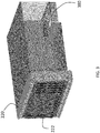
- FIG. 3 An application for a docking connector in accordance with the present invention may be referred to as a "secondary docking connector.”
- the interface system 100 has a plurality of printed circuit boards (PCB's) 310 mounted in a fixture 300.
- the system has a standard interface comprising a receiver or receivers 210 mounted to test equipment (not shown) and a fixture or enclosure 300 having one or more interchangeable test adapters (ITA) 220 that each mate with the receiver 210.
- PCB's printed circuit boards
- ITA interchangeable test adapters
- the test adapter 220 has a first plurality of modules 222 mounted in the test adapter 220, a plurality of PCB's 310 each having a first end connected to the first plurality of modules 222 and a secondary docking connector 380 having a second plurality of modules 350 connected to second ends of the plurality of PCB's.
- the modules 222 typically are each mounted to the test adapter frame with a screw at each end of the module.
- the enclosure or fixture 300 further has a cover 320 and supporting structure 330, 340.
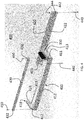
- one of the PCB's 310 is shown in a position in which it appears to have been pulled out through the front of the text adapter 220.
- a conventional docking connector however, even if the screws mounting the module 222 are removed and the module is removed the PCB 310 cannot be removed through the face of the test adapter 220 because movement of the second plurality of modules 350 in that direction is blocked by the secondary docking connector 380.
- the present invention solves this shortcoming by providing a "quick exchange" docking connector that allows the bottom bar of the docking connector to be quickly removed to allow the PCB's to slide directly out of the face of the test adapter 220.
- bottom bar here is used to refer to the side of the docking connector frame that is closest to the test adapter 220.
- the opposing side of the docking connector that is furthest form the test adapter 220 is referred to herein at the "top bar.”
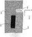
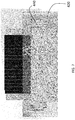
- the quick exchange docking connector 400 has a top bar 412 having an elongated portion and a perpendicular side portion 413 extending from each end of the elongated portion. Each side portion 413 has a mounting member 416 adapted to engage with a mounting member on a second elongated bar 430.
- a removable bottom bar 420 is connected to the top bar 412 via screws 440 placed through thru-hole 442 in a mounting member 423 on the bottom bar 420 and thru-hole 418 in the top bar and secured in threaded holes 444. When connected the top bar and the bottom bar form a rectangular frame in which modules may be mounted.
- the elongated portion of the top bar 412 has on its side facing the interior of the docking connector frame has a plurality of horseshoe-shaped grooves 414 each for receiving an end of a module 350.
- the bottom bar 420 has a groove along is length facing the interior of the frame for receiving a second end of each module.
- the two screws 440 are removed from the docking connector thereby freeing the bottom bar 420 to be moved in Direction A away from the top bar and then in direction B to be removed altogether. If the screws securing the modules 222 o the test adapter 220 are removed (either before or after removing the bottom bar o the docking connector, once the bottom bar 420 is removed the PCB's can slide directly out of the front of the test adapter.
- This quick exchange docking connector design provides for each removal of the PCB's from a fixture or enclosure for replacing, repairing, or otherwise servicing the PCB's.
Landscapes
- Engineering & Computer Science (AREA)
- Microelectronics & Electronic Packaging (AREA)
- Details Of Connecting Devices For Male And Female Coupling (AREA)
- Coupling Device And Connection With Printed Circuit (AREA)
Applications Claiming Priority (1)
| Application Number | Priority Date | Filing Date | Title |
|---|---|---|---|
| US201962889527P | 2019-08-20 | 2019-08-20 |
Publications (3)
| Publication Number | Publication Date |
|---|---|
| EP3784010A1 true EP3784010A1 (de) | 2021-02-24 |
| EP3784010C0 EP3784010C0 (de) | 2025-11-05 |
| EP3784010B1 EP3784010B1 (de) | 2025-11-05 |
Family
ID=72193261
Family Applications (1)
| Application Number | Title | Priority Date | Filing Date |
|---|---|---|---|
| EP20192032.9A Active EP3784010B1 (de) | 2019-08-20 | 2020-08-20 | Schnell austauschbarer andockanschluss |
Country Status (2)
| Country | Link |
|---|---|
| US (1) | US20210057843A1 (de) |
| EP (1) | EP3784010B1 (de) |
Citations (9)
| Publication number | Priority date | Publication date | Assignee | Title |
|---|---|---|---|---|
| US4583808A (en) * | 1985-03-05 | 1986-04-22 | Ncr Corporation | Configurable multiple connector panel |
| US20020137389A1 (en) * | 2001-03-26 | 2002-09-26 | Mac Panel Company | Connection interface system |
| US7091415B2 (en) | 2004-08-16 | 2006-08-15 | Virginia Panel Corporation | Low profile mass interconnect device |
| US7297014B1 (en) | 2006-07-10 | 2007-11-20 | Virginia Panel Corporation | Spring lock interface engagement system |
| US8351218B2 (en) | 2008-03-05 | 2013-01-08 | Virginia Panel Corporation | Multi-tier mass interconnect device |
| US8348693B2 (en) | 2009-11-09 | 2013-01-08 | Virginia Panel Corporation | Electrical connector interface with latch operated by threaded drive shaft |
| US20150087175A1 (en) * | 2013-09-25 | 2015-03-26 | Jeffery P Stowers | High Speed Data Module For High Life Cycle Interconnect Device |
| US9257787B2 (en) | 2009-02-03 | 2016-02-09 | Virginia Panel Corporation | Interface device |
| US20180358735A1 (en) | 2017-06-08 | 2018-12-13 | Virginia Panel Corporation | Configurable docking connector |
Family Cites Families (1)
| Publication number | Priority date | Publication date | Assignee | Title |
|---|---|---|---|---|
| ITMI20130462A1 (it) * | 2013-03-27 | 2014-09-28 | Westec S R L | Struttura di telaio di supporto per connettori modulari. |
-
2020
- 2020-08-20 US US16/998,233 patent/US20210057843A1/en not_active Abandoned
- 2020-08-20 EP EP20192032.9A patent/EP3784010B1/de active Active
Patent Citations (9)
| Publication number | Priority date | Publication date | Assignee | Title |
|---|---|---|---|---|
| US4583808A (en) * | 1985-03-05 | 1986-04-22 | Ncr Corporation | Configurable multiple connector panel |
| US20020137389A1 (en) * | 2001-03-26 | 2002-09-26 | Mac Panel Company | Connection interface system |
| US7091415B2 (en) | 2004-08-16 | 2006-08-15 | Virginia Panel Corporation | Low profile mass interconnect device |
| US7297014B1 (en) | 2006-07-10 | 2007-11-20 | Virginia Panel Corporation | Spring lock interface engagement system |
| US8351218B2 (en) | 2008-03-05 | 2013-01-08 | Virginia Panel Corporation | Multi-tier mass interconnect device |
| US9257787B2 (en) | 2009-02-03 | 2016-02-09 | Virginia Panel Corporation | Interface device |
| US8348693B2 (en) | 2009-11-09 | 2013-01-08 | Virginia Panel Corporation | Electrical connector interface with latch operated by threaded drive shaft |
| US20150087175A1 (en) * | 2013-09-25 | 2015-03-26 | Jeffery P Stowers | High Speed Data Module For High Life Cycle Interconnect Device |
| US20180358735A1 (en) | 2017-06-08 | 2018-12-13 | Virginia Panel Corporation | Configurable docking connector |
Also Published As
| Publication number | Publication date |
|---|---|
| US20210057843A1 (en) | 2021-02-25 |
| EP3784010C0 (de) | 2025-11-05 |
| EP3784010B1 (de) | 2025-11-05 |
Similar Documents
| Publication | Publication Date | Title |
|---|---|---|
| JP3949661B2 (ja) | ファイバ光学部品のための高密度モジューラ・バックプレーン・コネクタ | |
| EP2854239B1 (de) | Schnelles Datenmodul für Verbindungsvorrichtung mit hoher Lebensdauer | |
| US9160088B2 (en) | Backplane communication system and rack assembly of the same | |
| US20160286678A1 (en) | Housing for expansion cards | |
| US20170229825A1 (en) | Patch panel frame for circuit board module | |
| EP3413402A1 (de) | Konfigurierbarer andockverbinder | |
| US20180254571A1 (en) | Card edge connector assembly | |
| US8894438B2 (en) | Receptacle assembly having angled receptacle guide frames | |
| EP2929650B1 (de) | Netzwerkvorrichtung | |
| CA3007406A1 (en) | Coaxial connector assembly and communication system having a plurality of coaxial contacts | |
| EP0309127A2 (de) | Fiberoptischer Adapter | |
| US20170083057A1 (en) | VARIABLE WIDTH PCIe INTERFACE | |
| CA2821707A1 (en) | Line light irradiation device | |
| US4468858A (en) | Tool for separating mated connectors | |
| US8351218B2 (en) | Multi-tier mass interconnect device | |
| US8325488B2 (en) | Card module and module connector assembly | |
| US8760875B2 (en) | High density digital signal cross-connect system | |
| EP0443492A1 (de) | Steckverbinder mit geschützten Leistungskontakten | |
| EP3784010B1 (de) | Schnell austauschbarer andockanschluss | |
| JP6021619B2 (ja) | 光コネクタ、光コネクタシステム、光バックプレーン装置 | |
| WO2016068892A1 (en) | Optical connector assembly apparatus | |
| KR20090123410A (ko) | 솔리드 스테이트 디스크 스토리지 검사용 캐리 보드 조립체 | |
| US11611182B2 (en) | Exchangeable extended life connections for mass interconnects | |
| CN217902430U (zh) | 视野可调的读码器 | |
| CN219532449U (zh) | 一种光纤测试盒子 |
Legal Events
| Date | Code | Title | Description |
|---|---|---|---|
| PUAI | Public reference made under article 153(3) epc to a published international application that has entered the european phase |
Free format text: ORIGINAL CODE: 0009012 |
|
| STAA | Information on the status of an ep patent application or granted ep patent |
Free format text: STATUS: THE APPLICATION HAS BEEN PUBLISHED |
|
| AK | Designated contracting states |
Kind code of ref document: A1 Designated state(s): AL AT BE BG CH CY CZ DE DK EE ES FI FR GB GR HR HU IE IS IT LI LT LU LV MC MK MT NL NO PL PT RO RS SE SI SK SM TR |
|
| AX | Request for extension of the european patent |
Extension state: BA ME |
|
| STAA | Information on the status of an ep patent application or granted ep patent |
Free format text: STATUS: REQUEST FOR EXAMINATION WAS MADE |
|
| 17P | Request for examination filed |
Effective date: 20210824 |
|
| RBV | Designated contracting states (corrected) |
Designated state(s): AL AT BE BG CH CY CZ DE DK EE ES FI FR GB GR HR HU IE IS IT LI LT LU LV MC MK MT NL NO PL PT RO RS SE SI SK SM TR |
|
| STAA | Information on the status of an ep patent application or granted ep patent |
Free format text: STATUS: EXAMINATION IS IN PROGRESS |
|
| 17Q | First examination report despatched |
Effective date: 20221010 |
|
| GRAP | Despatch of communication of intention to grant a patent |
Free format text: ORIGINAL CODE: EPIDOSNIGR1 |
|
| STAA | Information on the status of an ep patent application or granted ep patent |
Free format text: STATUS: GRANT OF PATENT IS INTENDED |
|
| INTG | Intention to grant announced |
Effective date: 20250526 |
|
| GRAS | Grant fee paid |
Free format text: ORIGINAL CODE: EPIDOSNIGR3 |
|
| GRAA | (expected) grant |
Free format text: ORIGINAL CODE: 0009210 |
|
| STAA | Information on the status of an ep patent application or granted ep patent |
Free format text: STATUS: THE PATENT HAS BEEN GRANTED |
|
| AK | Designated contracting states |
Kind code of ref document: B1 Designated state(s): AL AT BE BG CH CY CZ DE DK EE ES FI FR GB GR HR HU IE IS IT LI LT LU LV MC MK MT NL NO PL PT RO RS SE SI SK SM TR |
|
| REG | Reference to a national code |
Ref country code: CH Ref legal event code: F10 Free format text: ST27 STATUS EVENT CODE: U-0-0-F10-F00 (AS PROVIDED BY THE NATIONAL OFFICE) Effective date: 20251105 Ref country code: GB Ref legal event code: FG4D |
|
| REG | Reference to a national code |
Ref country code: DE Ref legal event code: R096 Ref document number: 602020061555 Country of ref document: DE |
|
| REG | Reference to a national code |
Ref country code: IE Ref legal event code: FG4D |
|
| U01 | Request for unitary effect filed |
Effective date: 20251205 |
|
| U07 | Unitary effect registered |
Designated state(s): AT BE BG DE DK EE FI FR IT LT LU LV MT NL PT RO SE SI Effective date: 20251212 |
|
| PG25 | Lapsed in a contracting state [announced via postgrant information from national office to epo] |
Ref country code: ES Free format text: LAPSE BECAUSE OF FAILURE TO SUBMIT A TRANSLATION OF THE DESCRIPTION OR TO PAY THE FEE WITHIN THE PRESCRIBED TIME-LIMIT Effective date: 20251105 |
|
| PG25 | Lapsed in a contracting state [announced via postgrant information from national office to epo] |
Ref country code: NO Free format text: LAPSE BECAUSE OF FAILURE TO SUBMIT A TRANSLATION OF THE DESCRIPTION OR TO PAY THE FEE WITHIN THE PRESCRIBED TIME-LIMIT Effective date: 20260205 |
|
| PG25 | Lapsed in a contracting state [announced via postgrant information from national office to epo] |
Ref country code: HR Free format text: LAPSE BECAUSE OF FAILURE TO SUBMIT A TRANSLATION OF THE DESCRIPTION OR TO PAY THE FEE WITHIN THE PRESCRIBED TIME-LIMIT Effective date: 20251105 |
|
| PG25 | Lapsed in a contracting state [announced via postgrant information from national office to epo] |
Ref country code: RS Free format text: LAPSE BECAUSE OF FAILURE TO SUBMIT A TRANSLATION OF THE DESCRIPTION OR TO PAY THE FEE WITHIN THE PRESCRIBED TIME-LIMIT Effective date: 20260205 |
|
| PG25 | Lapsed in a contracting state [announced via postgrant information from national office to epo] |
Ref country code: IS Free format text: LAPSE BECAUSE OF FAILURE TO SUBMIT A TRANSLATION OF THE DESCRIPTION OR TO PAY THE FEE WITHIN THE PRESCRIBED TIME-LIMIT Effective date: 20260305 |
|
| PG25 | Lapsed in a contracting state [announced via postgrant information from national office to epo] |
Ref country code: PL Free format text: LAPSE BECAUSE OF FAILURE TO SUBMIT A TRANSLATION OF THE DESCRIPTION OR TO PAY THE FEE WITHIN THE PRESCRIBED TIME-LIMIT Effective date: 20251105 |