EP3787166B1 - Schutzschema für stromwandler mit kaskadierten zweipoligen und einpoligen leistungshalbleiterbauelementen - Google Patents
Schutzschema für stromwandler mit kaskadierten zweipoligen und einpoligen leistungshalbleiterbauelementen Download PDFInfo
- Publication number
- EP3787166B1 EP3787166B1 EP19194929.6A EP19194929A EP3787166B1 EP 3787166 B1 EP3787166 B1 EP 3787166B1 EP 19194929 A EP19194929 A EP 19194929A EP 3787166 B1 EP3787166 B1 EP 3787166B1
- Authority
- EP
- European Patent Office
- Prior art keywords
- igbts
- converter
- flying capacitor
- voltage
- comparator circuit
- Prior art date
- Legal status (The legal status is an assumption and is not a legal conclusion. Google has not performed a legal analysis and makes no representation as to the accuracy of the status listed.)
- Active
Links
Images



Classifications
-
- H—ELECTRICITY
- H02—GENERATION; CONVERSION OR DISTRIBUTION OF ELECTRIC POWER
- H02M—APPARATUS FOR CONVERSION BETWEEN AC AND AC, BETWEEN AC AND DC, OR BETWEEN DC AND DC, AND FOR USE WITH MAINS OR SIMILAR POWER SUPPLY SYSTEMS; CONVERSION OF DC OR AC INPUT POWER INTO SURGE OUTPUT POWER; CONTROL OR REGULATION THEREOF
- H02M1/00—Details of apparatus for conversion
- H02M1/32—Means for protecting converters other than automatic disconnection
-
- H—ELECTRICITY
- H02—GENERATION; CONVERSION OR DISTRIBUTION OF ELECTRIC POWER
- H02M—APPARATUS FOR CONVERSION BETWEEN AC AND AC, BETWEEN AC AND DC, OR BETWEEN DC AND DC, AND FOR USE WITH MAINS OR SIMILAR POWER SUPPLY SYSTEMS; CONVERSION OF DC OR AC INPUT POWER INTO SURGE OUTPUT POWER; CONTROL OR REGULATION THEREOF
- H02M7/00—Conversion of AC power input into DC power output; Conversion of DC power input into AC power output
- H02M7/42—Conversion of DC power input into AC power output without possibility of reversal
- H02M7/44—Conversion of DC power input into AC power output without possibility of reversal by static converters
- H02M7/48—Conversion of DC power input into AC power output without possibility of reversal by static converters using discharge tubes with control electrode or semiconductor devices with control electrode
- H02M7/483—Converters with outputs that each can have more than two voltages levels
-
- H—ELECTRICITY
- H02—GENERATION; CONVERSION OR DISTRIBUTION OF ELECTRIC POWER
- H02H—EMERGENCY PROTECTIVE CIRCUIT ARRANGEMENTS
- H02H7/00—Emergency protective circuit arrangements specially adapted for specific types of electric machines or apparatus or for sectionalised protection of cable or line systems, and effecting automatic switching in the event of an undesired change from normal working conditions
- H02H7/10—Emergency protective circuit arrangements specially adapted for specific types of electric machines or apparatus or for sectionalised protection of cable or line systems, and effecting automatic switching in the event of an undesired change from normal working conditions for converters; for rectifiers
- H02H7/12—Emergency protective circuit arrangements specially adapted for specific types of electric machines or apparatus or for sectionalised protection of cable or line systems, and effecting automatic switching in the event of an undesired change from normal working conditions for converters; for rectifiers for static converters or rectifiers
- H02H7/122—Emergency protective circuit arrangements specially adapted for specific types of electric machines or apparatus or for sectionalised protection of cable or line systems, and effecting automatic switching in the event of an undesired change from normal working conditions for converters; for rectifiers for static converters or rectifiers for inverters, i.e. DC/AC converters
- H02H7/1227—Emergency protective circuit arrangements specially adapted for specific types of electric machines or apparatus or for sectionalised protection of cable or line systems, and effecting automatic switching in the event of an undesired change from normal working conditions for converters; for rectifiers for static converters or rectifiers for inverters, i.e. DC/AC converters responsive to abnormalities in the output circuit, e.g. short circuit
-
- H—ELECTRICITY
- H02—GENERATION; CONVERSION OR DISTRIBUTION OF ELECTRIC POWER
- H02M—APPARATUS FOR CONVERSION BETWEEN AC AND AC, BETWEEN AC AND DC, OR BETWEEN DC AND DC, AND FOR USE WITH MAINS OR SIMILAR POWER SUPPLY SYSTEMS; CONVERSION OF DC OR AC INPUT POWER INTO SURGE OUTPUT POWER; CONTROL OR REGULATION THEREOF
- H02M1/00—Details of apparatus for conversion
- H02M1/0095—Hybrid converter topologies, e.g. NPC mixed with flying capacitor, thyristor converter mixed with MMC or charge pump mixed with buck
-
- H—ELECTRICITY
- H02—GENERATION; CONVERSION OR DISTRIBUTION OF ELECTRIC POWER
- H02M—APPARATUS FOR CONVERSION BETWEEN AC AND AC, BETWEEN AC AND DC, OR BETWEEN DC AND DC, AND FOR USE WITH MAINS OR SIMILAR POWER SUPPLY SYSTEMS; CONVERSION OF DC OR AC INPUT POWER INTO SURGE OUTPUT POWER; CONTROL OR REGULATION THEREOF
- H02M7/00—Conversion of AC power input into DC power output; Conversion of DC power input into AC power output
- H02M7/42—Conversion of DC power input into AC power output without possibility of reversal
- H02M7/44—Conversion of DC power input into AC power output without possibility of reversal by static converters
- H02M7/48—Conversion of DC power input into AC power output without possibility of reversal by static converters using discharge tubes with control electrode or semiconductor devices with control electrode
- H02M7/483—Converters with outputs that each can have more than two voltages levels
- H02M7/4835—Converters with outputs that each can have more than two voltages levels comprising two or more cells, each including a switchable capacitor, the capacitors having a nominal charge voltage which corresponds to a given fraction of the input voltage, and the capacitors being selectively connected in series to determine the instantaneous output voltage
-
- H—ELECTRICITY
- H02—GENERATION; CONVERSION OR DISTRIBUTION OF ELECTRIC POWER
- H02M—APPARATUS FOR CONVERSION BETWEEN AC AND AC, BETWEEN AC AND DC, OR BETWEEN DC AND DC, AND FOR USE WITH MAINS OR SIMILAR POWER SUPPLY SYSTEMS; CONVERSION OF DC OR AC INPUT POWER INTO SURGE OUTPUT POWER; CONTROL OR REGULATION THEREOF
- H02M7/00—Conversion of AC power input into DC power output; Conversion of DC power input into AC power output
- H02M7/42—Conversion of DC power input into AC power output without possibility of reversal
- H02M7/44—Conversion of DC power input into AC power output without possibility of reversal by static converters
- H02M7/48—Conversion of DC power input into AC power output without possibility of reversal by static converters using discharge tubes with control electrode or semiconductor devices with control electrode
- H02M7/483—Converters with outputs that each can have more than two voltages levels
- H02M7/4837—Flying capacitor converters
-
- H—ELECTRICITY
- H02—GENERATION; CONVERSION OR DISTRIBUTION OF ELECTRIC POWER
- H02M—APPARATUS FOR CONVERSION BETWEEN AC AND AC, BETWEEN AC AND DC, OR BETWEEN DC AND DC, AND FOR USE WITH MAINS OR SIMILAR POWER SUPPLY SYSTEMS; CONVERSION OF DC OR AC INPUT POWER INTO SURGE OUTPUT POWER; CONTROL OR REGULATION THEREOF
- H02M7/00—Conversion of AC power input into DC power output; Conversion of DC power input into AC power output
- H02M7/42—Conversion of DC power input into AC power output without possibility of reversal
- H02M7/44—Conversion of DC power input into AC power output without possibility of reversal by static converters
- H02M7/48—Conversion of DC power input into AC power output without possibility of reversal by static converters using discharge tubes with control electrode or semiconductor devices with control electrode
- H02M7/483—Converters with outputs that each can have more than two voltages levels
- H02M7/487—Neutral point clamped inverters
-
- H—ELECTRICITY
- H02—GENERATION; CONVERSION OR DISTRIBUTION OF ELECTRIC POWER
- H02M—APPARATUS FOR CONVERSION BETWEEN AC AND AC, BETWEEN AC AND DC, OR BETWEEN DC AND DC, AND FOR USE WITH MAINS OR SIMILAR POWER SUPPLY SYSTEMS; CONVERSION OF DC OR AC INPUT POWER INTO SURGE OUTPUT POWER; CONTROL OR REGULATION THEREOF
- H02M1/00—Details of apparatus for conversion
- H02M1/0003—Details of control, feedback or regulation circuits
- H02M1/0009—Devices or circuits for detecting current in a converter
-
- Y—GENERAL TAGGING OF NEW TECHNOLOGICAL DEVELOPMENTS; GENERAL TAGGING OF CROSS-SECTIONAL TECHNOLOGIES SPANNING OVER SEVERAL SECTIONS OF THE IPC; TECHNICAL SUBJECTS COVERED BY FORMER USPC CROSS-REFERENCE ART COLLECTIONS [XRACs] AND DIGESTS
- Y02—TECHNOLOGIES OR APPLICATIONS FOR MITIGATION OR ADAPTATION AGAINST CLIMATE CHANGE
- Y02B—CLIMATE CHANGE MITIGATION TECHNOLOGIES RELATED TO BUILDINGS, e.g. HOUSING, HOUSE APPLIANCES OR RELATED END-USER APPLICATIONS
- Y02B70/00—Technologies for an efficient end-user side electric power management and consumption
- Y02B70/10—Technologies improving the efficiency by using switched-mode power supplies [SMPS], i.e. efficient power electronics conversion e.g. power factor correction or reduction of losses in power supplies or efficient standby modes
Definitions
- Embodiments of the present disclosure generally relate to the field of Multilevel Power Converters.
- the disclosure in particular relates to the field of multilevel power converters with cascaded semiconductors like flying capacitor converters or clamped converters like Active Neutral Point Clamped (ANPC) converters.
- ANPC Active Neutral Point Clamped
- a method and a circuit arrangement is disclosed in the embodiments for protecting all the semiconductor devices in the converters from excessive currents.
- Multilevel Power converters are used to convert electric energy from one form to another such as converting between AC and DC; or changing the voltage or frequency; or some combination of these.
- Power MOSFETs are very advantageous for power electronic converters due to their fast switching capabilities and resistive conduction behavior.
- silicon based power MOSFETs generally suffer from limited voltage blocking capability.
- the body diode has a poor dynamic performance. For this reason silicon, IGBTs have partly replaced them especially in industrial applications.
- SiC Silicon carbide
- the SiC MOSFETs offer a comparable and even higher voltage blocking capability than state-of-the-art silicon based IGBTs, very low switching losses, bidirectional conduction capability with low conduction losses, and a body diode with good dynamic performance, which renders separate anti-parallel diodes unnecessary.
- the main disadvantage of the SiC MOSFETs is the poor short circuit capability.
- FC flying capacitor
- the converter phase leg needs to be built with a large number of series-connected devices to enable connection to standard residential and industrial low-voltage distributions systems.
- the total voltage blocking capability of a phase leg can be increased by increasing the number of the flying capacitor cells.
- the FC converter can be combined with a polarity selector stage (PSS) which halves the input voltage of the FC converter. This may reduce the number of the FC cells. Because the polarity selector stage operates at fundamental frequency, IGBTs with a high voltage blocking capability can be used.
- PSS polarity selector stage
- each active switch is individually protected against short circuits e.g. by a standard desaturation detection circuitry.
- GB 2 564 700 A discloses a module for detecting a fault in a solid state switching device of a power electronics module.
- a power electronics module e.g. inverter
- the gate driver connects to, and provides a drive input to, a gate terminal of the switching device to activate the switching device.
- the controller provides a gate signal to the gate driver.
- the fault detector includes a capacitor (e.g. external Miller capacitor, CM) connected to a collector terminal of the switching device and a comparator connected to the capacitor. The comparator compares a voltage received from the capacitor against a threshold voltage.
- CM Miller capacitor
- EP 3 188 355 A1 concerns a voltage converter including a first set of silicon (Si)-based power devices coupled to a first direct current (DC) voltage source and a second set of Si-based power devices coupled to a second DC voltage source.
- the voltage converter may also include a first set of silicon-carbide (SiC)-based power devices coupled to the first set of Si-based power devices and to the second set of Si-based power devices.
- SiC silicon-carbide
- Each SiC-based power device of the first set of SiC-based power devices may switch at a higher frequency as compared to each Si-based power device of the first and second sets of the Si-based power electronic devices.
- FREDERIC RICHARDEAU ET AL (IEEE TRANSACTIONS ON POWER ELECTRONICS. VOL- 17. NO. 6, NOVEMBER 2002 ) concerns considerations about short-circuit tolerance of an IGBT multicell inverter when a commutation failure occurs.
- Several failure cases are explained. aim of this paper is to explain the intrinsic short-circuit tolerance of an IGBT multicell inverter when a commutation failure occurs Such a failure may either be a wrong gate voltage (malfunctioning of the driver board, auxiliary power supply failure, dv/dt disturbance) or an intrinsic IGBT failure (over-voltage/avalanche stress, temperature overshoot).
- HONGGANG SHENG ET AL (IEEE TRANSACTIONS ON POWER ELECTRONICS, vol. 27, no. 2, February 2012 ) describes a fault detection and protection scheme for Three-Level DC-DC Converters based on monitoring flying capacitor voltage.
- a protection circuit according to claim 1 is disclosed.
- a power converter according to claim 9 is disclosed.
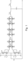
- FIG. 1 shows one phase leg of a power converter.
- the power converter in FIG. 1 is a converter according to the flying capacitor (FCC) concept.
- the FCC topology was developed in the 1990s, and it uses several floating capacitors instead of clamping diodes to share the voltage stress among devices and to achieve different voltage levels in the output.
- the FCC topology can be extended, achieving more levels in the output phase by the connection of more cells in tandem.
- a polarity selector stage formed of semiconductors 120 is arranged in the converter.
- the polarity selector stage halves the voltage input of the flying capacitor converter. With this measure, the number of FC cells needed is reduced.
- FC cells consist of semiconductors 130 and a capacitor (flying capacitor) 140. The semiconductors are operated complementarily.
- FIG. 1 shows a multitude of connected flying capacitor cells, symbolized by three FC cells separated by dotted lines.
- the FC cells form one phase leg.
- the phase leg is connected to a filter circuit comprising a quadripole (T-Network), comprising two inductors (L conv , L sup ) and one capacitor C 1 .
- the quadripole serves as a filter circuit to "smooth" the output current, which has a sinusoidal shape in the ideal case.
- FC converter technology employs a large number of active semiconductors, gate drivers and gate voltage supplies. Normally, each active semiconductor switch should be protected against short circuits, since in big installations high voltages and high currents are present.
- a common technology for monitoring and protecting the semiconductors is conventional standard desaturation detection circuitry.
- a protection circuit for a hybrid Active Neutral Point Clamped (ANPC) type power converter 100 with cascaded semiconductors 120, 130 is disclosed in a first embodiment of the present application.
- a polarity selection stage of the converter 100 comprises IGBTs 120, and at least two flying capacitor cells, arranged in the power converter 100, comprise each an arrangement of two MOSFET or SiCMOSFET type transistors 130 and a flying capacitor 140.
- the protection circuit comprises at least one comparator circuit 210, 310, 410, 420, adapted to monitor a voltage characteristic on a collector-emitter path of each of the IGBTs 120 arranged in the polarity selection stage (PSS) of the converter 100 and to monitor a voltage characteristic on the flying capacitor 140 of each of the at least two flying capacitor cells arranged in the power converter 100.
- PSS polarity selection stage
- the at least one comparator circuit 210, 310, 410, 420 is further adapted to output an electrical signal, representing the voltage characteristic of the IGBTs 120 and of the flying capacitor 140 of each of the at least two flying capacitor cells to at least one evaluation unit 220, 230, 320, 450, 520; wherein the at least one evaluation unit 220, 230, 320, 450, 520 is further adapted to evaluate the result from the at least one comparator circuit 210, 310, 410, 420 and to deactivate the IGBTs 120 of the polarity selection stage in case that the voltage characteristic of any of the IGBTs 120 and/or the flying capacitors of any of the flying capacitor cells 140 deviate from a predetermined threshold.
- the IGBTs can be utilized for overcurrent and/or short circuit protection. That is, excessive currents can be detected using e.g. a standard desaturation detection circuitry based on a collector-emitter voltage monitoring.
- the current flow from the main DC link to the FC converter stage is interrupted by turning off the IGBTs. If the switching frequency of the MOSFETs in the FC cells is high and therefore the capacitance of the flying capacitors small, the LV surface-mount MOSFETs are likely to withstand the energy stored in the flying capacitors and therefore no additional protection for the MOSFETs is necessary.
- the MOSFETs in the flying capacitor cells can be protected based on the flying capacitor cell voltage information. Even if no active cell voltage balancing is carried out, the cell voltages are typically measured for monitoring purposes. Thus, anomalies can be detected during operation based on sudden changes in the individual cell voltages, including flying capacitor cell voltage unbalances and over- and undervoltages, as well as MOSFETs failed in short or open circuit mode in the flying capacitor cells. A similar approach may be that a change rate of voltage is monitored to detect short circuits.
- ADC analog-to-digital converter
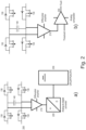
- FIG. 2a shows a flying capacitor (FC) cell.
- the cell may comprise semiconductors (MOSFETs) 130 and a capacitor 140 in a bridge like configuration. Two semiconductors 130 are respectively switched in a row, forming two branches. A capacitor 140 connects the two branches.
- a differential amplifier 210 having inputs. Two inputs are connected to first and second terminals of capacitor 140 as can be seen in FIG. 2a .
- the differential amplifier 210 having an output, connected to an input of an analog-to-digital converter 220, 515.
- the differential amplifier 210 evaluates a voltage behaviour of the capacitor 140 and feeds a signal of the evaluation to the A/D converter 220 which samples and digitizes the signal coming from the differential amplifier.
- the A/D converter 220 outputs a digital signal, comprising a behaviour of the voltage characteristic over the capacitor 140, to a calculation unit/FPGA/CPU 230 which is adapted to further analyse the signal from the A/D converter 220.
- FIG. 2b shows a similar arrangement with the difference that the differential amplifier 210 outputs its signal to a first input of an analog comparator 230.
- a predetermined signal acting as a threshold value is input into a second input of the analog comparator 230.
- the analog comparator outputs forward signal which may then be used for further purposes.
- the digital implementation enables more flexibility and use of advanced detection algorithms, but the analogue one may be more suitable for low-power and low-cost systems.
- Operation of the FC stage may be monitored by the FPGA based on the cell voltage measurements which are digitized with the ADCs. Sudden changes in the cell voltages may indicate a possible abnormal operation, e.g. shorted MOSFETs causing draining of a flying capacitor 140, overvoltage on the grid side etc.
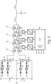
- An alternative method may be to monitor the voltage differences between adjacent cells as well as between the input and the first flying capacitor cell as can be seen in FIG. 3 .
- FIG. 3 shows an FC stage like it is shown in FIG. 2 , except that it has six semiconductors 130 from which respectively three semiconductors are switched in a row.
- Two capacitors 140 are arranged in a bridge like manner between the two branches comprising three semiconductors 130.
- the capacitor voltages are monitored, as in FIG. 2 , with a differential amplifier 310.
- an input voltage of the phase leg may be also monitored with a differential amplifier 310.
- Output signals of the three differential amplifiers 310 serve as input signals for two following differential amplifiers 310.
- These two differential amplifiers 310 generate output signals. Each of these output signals may be input in another analog comparator 320.
- the signal coming from the differential amplifier 310 may be compared with a threshold value.
- a failure signal FLT1 or FLT2 may be generated.
- the FPGA may additionally provide a gate control for the IGBTs (this is not shown in FIG. 5 ).
- the FPGA monitors the collector-emitter voltage of the IGBTs with the circuit consisting of a diode, a resistor and a Schmitt trigger. This logic signal may be used to detect desaturation by checking if the collector-emitter voltage drops fast enough after the IGBT is turned on. If the state of the logic signal does not change within a pre-defined time, this indicates a short circuit event.
- the circuit shown in FIG. 5 is simplified.
- the at least one comparator circuit 210, 310, 410, 420 may comprise an arrangement of a Schmitt-Trigger, a diode and a resistor.
- a circuit comprising a Schmitt trigger generates a status signal indicating the state of the IGBT based on the collector-emitter voltage, i.e. on or off (binary 1 or 0).
- the comparative operation may be carried out internally by the FPGA/CPU, which is time-based, and not voltage level-based as in the case of analog comparators.
- the FPGA can directly shutdown the IGBTs via signal outputs.
- the fault trigger can originate from any source, e.g. from the FC stage voltage monitoring, the IGBT desaturation protection, etc.
- any logic circuit or a CPU with a fast input capture function can be used.
- FIG. 7 A practical implementation 700 of a Schmitt trigger circuit 740 with some protection diodes (incl. a Zener diode 750), a filter capacitor 720, and a resistive voltage divider 730 to set a Schmitt trigger input voltage is shown in FIG. 7 .
- Terminal C is the point which connects to the resistor in FIG. 5
- terminal E is an IGBT emitter connection
- VCC a desired auxiliary voltage for the logic (e.g. 3.3 V) referenced to the emitter potential E.
- the at least one comparator circuit 210, 310, 410, 420 may comprise a differential amplifier. After the IGBT is turned on, the measured collector-emitter voltage may be compared in the differential amplifier to a pre-defined voltage level after a pre-defined time period to detect desaturation.
- FIG. 4 shows two simplified implementation examples for collector-emitter voltage monitoring. The most common one is based on an analog comparator which triggers the fault state if the IGBT collector-emitter voltage does not drop below the pre-set threshold when the IGBT is turned on ( FIG. 4a ).
- the IGBTs 120 are in the polarity selection stage.
- the four IGBTs 120 which are shown, are complementary switched. That means, the IGBTs can be activated only in specific configurations to avoid a short circuit of the DC link capacitors 110 which would destroy the IGBTs.
- Schmitt triggers have the purpose to form a digital signal from an analog signal by assigning a 0 or 1 two specific levels of the analog signal. Schmitt triggers and fast digital signal isolators guarantee a very small signal propagation delay.
- FC cell voltage monitoring there is no functional difference between analog and digital implementation. In both cases, voltage levels are monitored and compared.
- the at least one evaluation unit 220, 230, 320, 450, 520 may comprise an FPGA and/or a processor based control unit.
- the FPGA and/or the processor based control unit may comprise I/O terminals to receive values, representing e.g. voltage or current values from the least one comparator circuit 210, 310, 410, 420, 510 and to output control signals to control an activation state of the semiconductors 120, 130.
- the power converter is a converter according to a flying capacitor type.
- the flying capacitor converter may comprise at least two flying capacitor cells.
- the at least two cells in the flying capacitor converter may comprise an arrangement of at least two semiconductors 130 and a capacitor 140.
- an output of the IGBT stage is 550 V (each of the capacitors 110 in the PSS has half of the input voltage), which is also the input voltage of the FC stage.
- steady-state voltages of the FC cells are in an ideal case 412.5 V, 275 V and 137.5 V, starting from the cell closest to the DC input (left side).
- the protection concept provided in the present application may also be used in a further embodiment of the protection circuit, according to one or more other aspects, with other converter topologies comprising cascaded bipolar and unipolar devices.
- Such a converter type may be a converter type according to an Active Neutral Point Clamped (ANPC) Converter type.
- ANPC Active Neutral Point Clamped
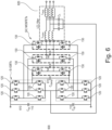
- FIG. 6 a 3-level hybrid Si/SiC active neutral point clamped (ANPC) converter consisting of silicon IGBTs and SiC MOSFETs is shown in FIG. 6 .
- the converter in FIG. 3 is a bi- directional three phase converter, which can be used to supply a three phase grid with power from e.g. a DC source (e.g. a solar plant).
- a DC source e.g. a solar plant
- the IGBT 120 stage acts as polarity selector stage operating at the fundamental frequency, whereas the SiC MOSFETs are pulse width modulated at high frequency.
- the poor short circuit capability of SiC MOSFETs can be overcome by utilizing the saturation characteristics of the IGBTs to limit the short circuit current flowing through the SiC MOSFETs.
- the energy in the voltage clamping capacitors (C clamp ) 140 is typically not high enough to destroy the SiC MOSFETs in case of short circuit only, it is sufficient that the current flow from the main dc link is interrupted by turning off the IGBTs. Therefore, only the IGBT stage needs to be equipped with a short circuit detection circuitry, e.g.
- the semiconductors 130 may also be MOSFET or SiC MOSFET type transistors, in particular when the semiconductors are used in an FC cell or as a clamping capacitor in an active neutral point clamped (ANPC) converter.
- ANPC active neutral point clamped
- a method for protecting a hybrid Active Neutral Point Clamped (ANPC) type power converter 100 with cascaded semiconductors 120, 130 is disclosed.
- a polarity selection stage of the converter 100 comprises IGBTs 120, and at least two flying capacitor cells, arranged in the power converter 100, each comprise an arrangement of two MOSFET or SiCMOSFET type transistors 130 and a flying capacitor 140.
- the method comprises to determine, with at least a first comparator circuit 210, 310, 410, 420, a voltage characteristic on terminals of each of the IGBTs 120and determining, with at least a second comparator circuit 210, 310, 410, 420, a voltage characteristic on terminals of each of the two or more flying capacitors 140 in the power converter.
- the method further comprises to evaluate, with one or more evaluation units 220, 230, 320, 450, 520, if the voltage characteristic on the terminals of any of the IGBTs 120 and if the voltage characteristic on the terminals of any of the two or more flying capacitors 140 in the power converter deviates from a predetermined threshold.
- the method further comprises to deactivate, with a deactivating unit, the IGBTs 120, when said voltage characteristics deviate from predetermined thresholds, to interrupt a current flow through the power converter. That means in other words, the voltage characteristics in a steady or normal operation modus is known and serves as reference values to decide if a deactivation is necessary or not.
- Some acceptable deviations e.g. in voltage or current may be stored as data in a memory of a controller which may control e.g. voltage behavior, rise time, fall time over the capacitors, current characteristic and other electrical values thereof from which a proper operation state can be derived. If perhaps, for any reason, a voltage, e.g. measured over the capacitors, does not fit such predetermined values, the semiconductors 120 are deactivated and a current flow is therefore interrupted.
- the at least one comparator circuit 210, 310, 410, 420 may comprise an arrangement of a Schmitt-Trigger, a diode and a resistor 530, 540, 550, 560.
- the at least one comparator circuit 210, 310, 410, 420 may comprise at least one differential amplifier.
- the at least one evaluation unit 220, 230, 320, 450, 520 may comprise an FPGA and/or a processor based control unit.
- the FPGA and/or the processor based control unit may further comprise I/O terminals, adapted to receive values from the least one comparator circuit 210, 310, 410, 420.
- the FPGA and/or the processor based control unit may further be adapted to output control signals to control an activation state of the semiconductors 120, 130.
- the FPGA and/or the processor based control unit may have the possibility to switch off (deactivate) the semiconductors 120, 130.
- Yet a further embodiment is a multilevel power converter with cascaded bipolar and/or unipolar semiconductors 120, 130, comprising a protection circuit according to one or more aspects of the present applications.
- a protection concept for multilevel converters comprising cascaded semiconductors is disclosed in the foregoing.
- the protection concept focuses mainly on a combination of a protection of IGBTs in a polarity selection stage of the converter.
- monitoring characteristics of cell voltages and or voltage characteristics of the flying capacitors is also considered in the protection concept.
- the IGBTs in the polarity selection stage are monitored with e.g. desaturation control circuits. In case these desaturation control circuits signalise an IGBT becoming defective, the IGBTs in the polarity selection stage are switched off like a main fuse to protect the following converter stages.
- the IGBT 120 collector-emitter voltages are monitored to detect short circuits in the phase current path and to avoid shoot-through of the main dc energy storage in case of IGBT failure.
- the FPGA receives the instantaneous switching states of the IGBTs and checks that each device turns on properly when the gate voltage is applied. In case the collector-emitter voltage does not drop fast enough after the gate has been turned on, a short circuit fault is triggered and the modulation stopped.
- the circuit monitoring the cell voltages, then also gives the command to switch off the IGBTs. This interrupts the current flow through the FC cells and therefore through the converter/converter leg.
Landscapes
- Engineering & Computer Science (AREA)
- Power Engineering (AREA)
- Protection Of Static Devices (AREA)
- Power Conversion In General (AREA)
- Inverter Devices (AREA)
Claims (9)
- Schutzschaltung für einen hybriden Leistungsumsetzer (100) des aktiven Typs mit geklemmtem Neutralpunkt (ANPC-Typ) mit kaskadierten Halbleitern (120, 130), wobei eine Polaritätsauswahlstufe des Umsetzers (100) IGBTs (120) umfasst und mindestens zwei fliegende Kondensatorzellen, die im Leistungsumsetzer (100) angeordnet sind, jeweils eine Anordnung von zwei Transistoren (130) des MOSFET- oder SiCMOSFET-Typs und einen fliegenden Kondensator (140) umfassen; wobei die Schutzschaltung Folgendes umfasst:mindestens eine Komparatorschaltung (210, 310, 410, 420, 510), die ausgelegt ist, eine Spannungscharakteristik in einem Kollektor/Emitter-Pfad jedes der IGBTs (120), die in der Polaritätsauswahlstufe des Umsetzers (100) angeordnet sind, zu überwachen, undeine Spannungscharakteristik an dem fliegenden Kondensator (140) jeder der mindestens zwei fliegenden Kondensatorzellen, die im Leistungsumsetzer (100) angeordnet sind, zu überwachen; wobeidie mindestens eine Komparatorschaltung (210, 310, 410, 420) ferner ausgelegt ist, ein elektrisches Signal, das die Spannungscharakteristik der IGBTs (120) und des fliegenden Kondensators (140) jeder der mindestens zwei fliegenden Kondensatorzellen repräsentiert, zu mindestens einer Bewertungseinheit (220, 230, 320, 450, 520) auszugeben; unddie mindestens eine Bewertungseinheit (220, 230, 320, 450, 520) ferner ausgelegt ist, das Ergebnis der mindestens einen Komparatorschaltung (210, 310, 410, 420) zu bewerten und die IGBTs (120) der Polaritätsauswahlstufe zu deaktivieren, falls die Spannungscharakteristik eines der IGBTs (120) und/oder der fliegenden Kondensatoren (140) einer der fliegenden Kondensatorzellen von einem vorgegebenen Schwellenwert abweicht.
- Schutzschaltung nach Anspruch 1, wobei die mindestens eine Komparatorschaltung (210, 310, 410, 420) eine Anordnung eines Schmitt-Triggers, einer Diode und eines Widerstands umfasst.
- Schutzschaltung nach Anspruch 1, wobei die mindestens eine Komparatorschaltung (210, 310, 410, 420) einen Differenzverstärker umfasst.
- Schutzschaltung nach Anspruch 1, wobei die mindestens eine Bewertungseinheit (220, 230, 320, 450, 520) ein FPGA und/oder eine prozessorbasierte Steuereinheit umfasst; wobei
das FPGA und/oder die prozessorbasierte Steuereinheit Eingangs-/Ausgangs-Anschlüsse umfassen, um Werte von der mindestens einen Komparatorschaltung (210, 310, 410, 420) zu empfangen und Steuersignale auszugeben, um einen Aktivierungszustand der Halbleiter (120, 130) zu steuern. - Verfahren zum Schützen eines hybriden Leistungsumsetzers (100) des aktiven Typs mit geklemmtem Neutralpunkt (ANPC-Typ) mit kaskadierten Halbleitern (120, 130); wobei eine Polaritätsauswahlstufe des Umsetzers (100) IGBTs (120) umfasst und mindestens zwei fliegende Kondensatorzellen, die im Leistungsumsetzer (100) angeordnet sind, jeweils eine Anordnung von zwei Transistoren (130) des MOSFET- oder SiCMOSFET-Typs und einen fliegenden Kondensator (140) umfassen; wobei die Schutzschaltung Folgendes umfasst:Bestimmen mit mindestens einer ersten Komparatorschaltung (210, 310, 410, 420) einer Spannungscharakteristik an Anschlüssen jedes der IGBTs (120) und Bestimmen mit mindestens einer zweiten Komparatorschaltung (210, 310, 410, 420) einer Spannungscharakteristik an Anschlüssen jedes der zwei oder mehr fliegenden Kondensatoren (140) im Leistungsumsetzer;Bewerten mit einer oder mehreren Bewertungseinheiten (220, 230, 320, 450, 520), ob die Spannungscharakteristik an den Anschlüssen eines der IGBTs (120) und die Spannungscharakteristik an den Anschlüssen eines der zwei oder mehr fliegenden Kondensatoren (140) im Leistungsumsetzer von einem vorgegebenen Schwellenwert abweichen; undDeaktivieren mit einer Deaktivierungseinheit der IGBTs (120), falls irgendeine Spannungscharakteristik von vorgegebenen Schwellenwerten abweicht, um einen Stromfluss durch den Leistungsumsetzer zu unterbrechen.
- Verfahren nach Anspruch 5, wobei die mindestens eine Komparatorschaltung (210, 310, 410, 420) eine Anordnung eines Schmitt-Triggers, einer Diode und eines Widerstands umfasst.
- Verfahren nach Anspruch 5, wobei die mindestens eine Komparatorschaltung (210, 310, 410, 420) mindestens einen Differenzverstärker umfasst.
- Verfahren nach Anspruch 5, wobei die mindestens eine Bewertungseinheit (220, 230, 320, 450, 520) ein FPGA und/oder eine prozessorbasierte Steuereinheit umfasst;
wobei
das FPGA und/oder die prozessorbasierte Steuereinheit Eingangs-/Ausgangs-Anschlüsse umfassen, um Werte von der mindestens einen Komparatorschaltung (210, 310, 410, 420) zu empfangen und Steuersignale auszugeben, um einen Aktivierungszustand der Halbleiter (120, 130) zu steuern. - Hybrider Leistungsumsetzer des aktiven Typs mit geklemmtem Neutralpunkt (ANPC-Typ) mit kaskadierten bipolaren und/oder unipolaren Halbleitern (120, 130), die eine Schutzschaltung nach den Ansprüchen 1 bis 4 umfassen.
Priority Applications (3)
| Application Number | Priority Date | Filing Date | Title |
|---|---|---|---|
| EP19194929.6A EP3787166B1 (de) | 2019-09-02 | 2019-09-02 | Schutzschema für stromwandler mit kaskadierten zweipoligen und einpoligen leistungshalbleiterbauelementen |
| US17/009,135 US11563370B2 (en) | 2019-09-02 | 2020-09-01 | Protection scheme for power converters utilizing cascaded bipolar and unipolar power semiconductor devices |
| CN202010903501.6A CN112532090B (zh) | 2019-09-02 | 2020-09-01 | 利用级联双极和单极功率半导体的功率转换器的保护方案 |
Applications Claiming Priority (1)
| Application Number | Priority Date | Filing Date | Title |
|---|---|---|---|
| EP19194929.6A EP3787166B1 (de) | 2019-09-02 | 2019-09-02 | Schutzschema für stromwandler mit kaskadierten zweipoligen und einpoligen leistungshalbleiterbauelementen |
Publications (3)
| Publication Number | Publication Date |
|---|---|
| EP3787166A1 EP3787166A1 (de) | 2021-03-03 |
| EP3787166C0 EP3787166C0 (de) | 2024-05-01 |
| EP3787166B1 true EP3787166B1 (de) | 2024-05-01 |
Family
ID=67840993
Family Applications (1)
| Application Number | Title | Priority Date | Filing Date |
|---|---|---|---|
| EP19194929.6A Active EP3787166B1 (de) | 2019-09-02 | 2019-09-02 | Schutzschema für stromwandler mit kaskadierten zweipoligen und einpoligen leistungshalbleiterbauelementen |
Country Status (3)
| Country | Link |
|---|---|
| US (1) | US11563370B2 (de) |
| EP (1) | EP3787166B1 (de) |
| CN (1) | CN112532090B (de) |
Families Citing this family (11)
| Publication number | Priority date | Publication date | Assignee | Title |
|---|---|---|---|---|
| CN115088171B (zh) * | 2019-12-31 | 2025-10-28 | Abb瑞士股份有限公司 | 用于操作具有浮置单元的功率电子转换器设备的方法 |
| EP4111827B1 (de) * | 2020-02-27 | 2024-11-20 | Signify Holding B.V. | Hybrid-schaltkondensatorschaltung mit automatischem ladungsausgleich |
| US11770066B2 (en) | 2021-06-11 | 2023-09-26 | Hamilton Sundstrand Corporation | Protection circuitry for power converters |
| EP4106125A1 (de) * | 2021-06-18 | 2022-12-21 | Carrier Fire & Security EMEA BV | Kurzschlussisolierer |
| EP4148964A1 (de) | 2021-09-14 | 2023-03-15 | ABB E-mobility B.V. | Verfahren und vorrichtung zur kompensation eines fehlerhaften schalters in einem mehrstufigen flugkondensatorumrichter |
| US12101038B2 (en) * | 2021-11-22 | 2024-09-24 | Abb Schweiz Ag | Uninterruptible power supply having short circuit load capability |
| JP7720986B2 (ja) * | 2022-03-09 | 2025-08-08 | 三菱電機株式会社 | 電力変換装置 |
| CN116050255B (zh) * | 2022-12-26 | 2026-04-21 | 北京交通大学 | 超级电容支路模型支路数量计算方法及模型构建方法 |
| EP4456395A1 (de) * | 2023-04-26 | 2024-10-30 | Abb Schweiz Ag | Flying-capacitor-konverter und verfahren zum schutz eines flying-capacitor-konverters |
| DE102023212612A1 (de) * | 2023-12-13 | 2025-06-18 | Robert Bosch Gesellschaft mit beschränkter Haftung | Teilnehmerstation für ein serielles Bussystem und Verfahren zur Kommunikation mit differentiellen Signalen in einem seriellen Bussystem |
| DE102024200624A1 (de) * | 2024-01-24 | 2025-01-02 | Zf Friedrichshafen Ag | Wechselrichter, Verfahren und Vorrichtung zum Betreiben eines Wechselrichters |
Family Cites Families (20)
| Publication number | Priority date | Publication date | Assignee | Title |
|---|---|---|---|---|
| JP6040582B2 (ja) * | 2012-06-14 | 2016-12-07 | 富士電機株式会社 | マルチレベル電力変換回路の保護制御方式 |
| JP6111541B2 (ja) * | 2012-07-09 | 2017-04-12 | 富士電機株式会社 | マルチレベル電力変換回路の制御方式 |
| US9356536B2 (en) * | 2013-01-11 | 2016-05-31 | ABBI Research Ltd. | Bidirectional power conversion with fault-handling capability |
| US9595889B2 (en) * | 2013-02-15 | 2017-03-14 | Eaton Corporation | System and method for single-phase and three-phase current determination in power converters and inverters |
| DE102013218207A1 (de) * | 2013-09-11 | 2015-03-12 | Siemens Aktiengesellschaft | Modularer Mehrpunktstromrichter für hohe Spannungen |
| DE102013221900A1 (de) * | 2013-10-29 | 2015-04-30 | Robert Bosch Gmbh | Überspannungsschutzschaltung für einen Leistungshalbleiter und Verfahren zum Schutz eines Leistungshalbleiters vor Überspannungen |
| US9948177B2 (en) * | 2015-01-07 | 2018-04-17 | Philips Lighting Holding B.V. | Power conversion device |
| US10732685B2 (en) * | 2015-02-27 | 2020-08-04 | Ge Energy Power Conversion Technology Limited | System and method for operating power converters |
| US10367428B2 (en) * | 2015-06-15 | 2019-07-30 | Toshiba Mitsubishi-Electric Industrial Systems Corporation | Power conversion device |
| US10191531B2 (en) * | 2015-12-29 | 2019-01-29 | General Electric Company | Hybrid converter system |
| CN107276378B (zh) * | 2016-04-08 | 2019-03-15 | 台达电子企业管理(上海)有限公司 | 预先充电控制方法 |
| CN107306083B (zh) * | 2016-04-22 | 2019-09-20 | 台达电子企业管理(上海)有限公司 | 飞跨电容的电压平衡控制装置与电压平衡控制方法 |
| US9979322B2 (en) * | 2016-06-24 | 2018-05-22 | General Electric Company | Modulator for a hybrid converter system |
| US10868529B2 (en) * | 2016-09-30 | 2020-12-15 | Infineon Technologies Austria Ag | System and method for an overpower detector |
| US10263412B2 (en) * | 2016-12-22 | 2019-04-16 | Infineon Technologies Austria Ag | System and method for desaturation detection |
| US10581342B2 (en) * | 2017-07-10 | 2020-03-03 | General Electric Company | Three-level two-stage decoupled active NPC converter |
| GB2564700A (en) * | 2017-07-21 | 2019-01-23 | Rolls Royce Plc | A power electronics module and a method of detecting a fault in a power electronics module |
| GB2564701A (en) * | 2017-07-21 | 2019-01-23 | Rolls Royce Plc | A power electronics module and a method of protecting a solid state switching device in a power electronics module |
| US10924031B2 (en) * | 2018-05-22 | 2021-02-16 | The Governors Of The University Of Alberta | Internal paralleled active neutral point clamped converter with logic-based flying capacitor voltage balancing |
| US10784857B1 (en) * | 2019-05-31 | 2020-09-22 | Texas Instruments Incorporated | Adaptive gate drivers and related methods and systems |
-
2019
- 2019-09-02 EP EP19194929.6A patent/EP3787166B1/de active Active
-
2020
- 2020-09-01 US US17/009,135 patent/US11563370B2/en active Active
- 2020-09-01 CN CN202010903501.6A patent/CN112532090B/zh active Active
Non-Patent Citations (3)
| Title |
|---|
| AZURZA ANDERSON JON ET AL: "All-Silicon 99.35% Efficient Three-Phase Seven-Level Hybrid Neutral Point Clamped/Flying Capacitor Inverter", CPSS TRANSACTIONS ON POWER ELECTRONICS AND APPLICATIONS, vol. 4, no. 1, 1 March 2019 (2019-03-01), pages 50 - 61, XP093087999, ISSN: 2475-742X, DOI: 10.24295/CPSSTPEA.2019.00006 * |
| HONGGANG SHENG ET AL: "A Fault Detection and Protection Scheme for Three-Level DC DC Converters Based on Monitoring Flying Capacitor Voltage", IEEE TRANSACTIONS ON POWER ELECTRONICS, INSTITUTE OF ELECTRICAL AND ELECTRONICS ENGINEERS, USA, vol. 27, no. 2, 1 February 2012 (2012-02-01), pages 685 - 697, XP011406663, ISSN: 0885-8993, DOI: 10.1109/TPEL.2011.2161333 * |
| KONSTANTINOU G ET AL: "The seven-level flying capacitor based ANPC converter for grid intergration of utility-scale PV systems", POWER ELECTRONICS FOR DISTRIBUTED GENERATION SYSTEMS (PEDG), 2012 3RD IEEE INTERNATIONAL SYMPOSIUM ON, IEEE, 25 June 2012 (2012-06-25), pages 592 - 597, XP032226622, ISBN: 978-1-4673-2021-4, DOI: 10.1109/PEDG.2012.6254062 * |
Also Published As
| Publication number | Publication date |
|---|---|
| US20210119442A1 (en) | 2021-04-22 |
| EP3787166A1 (de) | 2021-03-03 |
| CN112532090A (zh) | 2021-03-19 |
| EP3787166C0 (de) | 2024-05-01 |
| CN112532090B (zh) | 2024-08-02 |
| US11563370B2 (en) | 2023-01-24 |
Similar Documents
| Publication | Publication Date | Title |
|---|---|---|
| EP3787166B1 (de) | Schutzschema für stromwandler mit kaskadierten zweipoligen und einpoligen leistungshalbleiterbauelementen | |
| US10186952B2 (en) | Power conversion device | |
| US8411474B2 (en) | System and method for protection of a multilevel converter | |
| US8471584B2 (en) | Switching device failure detection system and method for multilevel converters | |
| CN101548461B (zh) | 在电压中间电路变流器中用于控制直流侧的短路的半导体保护元件 | |
| US10003273B2 (en) | Power conversion device | |
| US10396678B2 (en) | Power converter | |
| EP2822173B1 (de) | Indirekter matrixwandler | |
| KR20220024907A (ko) | 플라잉 커패시터 기반 벅 부스트 컨버터를 위한 단락 보호 시스템 및 방법 | |
| CN112640238B (zh) | 用于识别高压直流输电线路中的故障并且生成用于直流断路器的触发信号的方法和设备 | |
| JPH114150A (ja) | 半導体装置とこの半導体装置を用いた電力変換装置 | |
| US9369035B2 (en) | Power converter and method of operation | |
| KR102699856B1 (ko) | 전원 장치 | |
| US12255546B2 (en) | Power conversion device that converts electric power between DC circuit and AC circuit | |
| US11394200B2 (en) | Device and method for coupling two DC grids | |
| JP6455719B2 (ja) | 無停電電源システム | |
| CN118868651A (zh) | 飞跨电容器转换器以及用于保护飞跨电容器转换器的方法 | |
| JP3722649B2 (ja) | 3レベルインバータ | |
| JP7414380B2 (ja) | 電力変換装置 | |
| CN118783391B (zh) | 一种具有lc故障耐受结构的光伏变换系统 | |
| JP2004088858A (ja) | 電力変換装置 | |
| CN223141606U (zh) | 储能阀子模块及储能系统 | |
| RU2456739C1 (ru) | Устройство многоуровневой защиты двунаправленного инвертора напряжения | |
| JP2025067140A (ja) | 電力変換装置 |
Legal Events
| Date | Code | Title | Description |
|---|---|---|---|
| PUAI | Public reference made under article 153(3) epc to a published international application that has entered the european phase |
Free format text: ORIGINAL CODE: 0009012 |
|
| STAA | Information on the status of an ep patent application or granted ep patent |
Free format text: STATUS: THE APPLICATION HAS BEEN PUBLISHED |
|
| AK | Designated contracting states |
Kind code of ref document: A1 Designated state(s): AL AT BE BG CH CY CZ DE DK EE ES FI FR GB GR HR HU IE IS IT LI LT LU LV MC MK MT NL NO PL PT RO RS SE SI SK SM TR |
|
| AX | Request for extension of the european patent |
Extension state: BA ME |
|
| STAA | Information on the status of an ep patent application or granted ep patent |
Free format text: STATUS: REQUEST FOR EXAMINATION WAS MADE |
|
| 17P | Request for examination filed |
Effective date: 20210903 |
|
| RBV | Designated contracting states (corrected) |
Designated state(s): AL AT BE BG CH CY CZ DE DK EE ES FI FR GB GR HR HU IE IS IT LI LT LU LV MC MK MT NL NO PL PT RO RS SE SI SK SM TR |
|
| STAA | Information on the status of an ep patent application or granted ep patent |
Free format text: STATUS: EXAMINATION IS IN PROGRESS |
|
| 17Q | First examination report despatched |
Effective date: 20220804 |
|
| GRAP | Despatch of communication of intention to grant a patent |
Free format text: ORIGINAL CODE: EPIDOSNIGR1 |
|
| STAA | Information on the status of an ep patent application or granted ep patent |
Free format text: STATUS: GRANT OF PATENT IS INTENDED |
|
| INTG | Intention to grant announced |
Effective date: 20231220 |
|
| GRAS | Grant fee paid |
Free format text: ORIGINAL CODE: EPIDOSNIGR3 |
|
| GRAA | (expected) grant |
Free format text: ORIGINAL CODE: 0009210 |
|
| STAA | Information on the status of an ep patent application or granted ep patent |
Free format text: STATUS: THE PATENT HAS BEEN GRANTED |
|
| AK | Designated contracting states |
Kind code of ref document: B1 Designated state(s): AL AT BE BG CH CY CZ DE DK EE ES FI FR GB GR HR HU IE IS IT LI LT LU LV MC MK MT NL NO PL PT RO RS SE SI SK SM TR |
|
| REG | Reference to a national code |
Ref country code: GB Ref legal event code: FG4D |
|
| REG | Reference to a national code |
Ref country code: CH Ref legal event code: EP |
|
| REG | Reference to a national code |
Ref country code: IE Ref legal event code: FG4D |
|
| REG | Reference to a national code |
Ref country code: DE Ref legal event code: R096 Ref document number: 602019051243 Country of ref document: DE |
|
| U01 | Request for unitary effect filed |
Effective date: 20240522 |
|
| U07 | Unitary effect registered |
Designated state(s): AT BE BG DE DK EE FI FR IT LT LU LV MT NL PT SE SI Effective date: 20240603 |
|
| PG25 | Lapsed in a contracting state [announced via postgrant information from national office to epo] |
Ref country code: IS Free format text: LAPSE BECAUSE OF FAILURE TO SUBMIT A TRANSLATION OF THE DESCRIPTION OR TO PAY THE FEE WITHIN THE PRESCRIBED TIME-LIMIT Effective date: 20240901 |
|
| PG25 | Lapsed in a contracting state [announced via postgrant information from national office to epo] |
Ref country code: HR Free format text: LAPSE BECAUSE OF FAILURE TO SUBMIT A TRANSLATION OF THE DESCRIPTION OR TO PAY THE FEE WITHIN THE PRESCRIBED TIME-LIMIT Effective date: 20240501 |
|
| PG25 | Lapsed in a contracting state [announced via postgrant information from national office to epo] |
Ref country code: GR Free format text: LAPSE BECAUSE OF FAILURE TO SUBMIT A TRANSLATION OF THE DESCRIPTION OR TO PAY THE FEE WITHIN THE PRESCRIBED TIME-LIMIT Effective date: 20240802 |
|
| PG25 | Lapsed in a contracting state [announced via postgrant information from national office to epo] |
Ref country code: ES Free format text: LAPSE BECAUSE OF FAILURE TO SUBMIT A TRANSLATION OF THE DESCRIPTION OR TO PAY THE FEE WITHIN THE PRESCRIBED TIME-LIMIT Effective date: 20240501 |
|
| PG25 | Lapsed in a contracting state [announced via postgrant information from national office to epo] |
Ref country code: PL Free format text: LAPSE BECAUSE OF FAILURE TO SUBMIT A TRANSLATION OF THE DESCRIPTION OR TO PAY THE FEE WITHIN THE PRESCRIBED TIME-LIMIT Effective date: 20240501 |
|
| U20 | Renewal fee for the european patent with unitary effect paid |
Year of fee payment: 6 Effective date: 20240925 |
|
| PG25 | Lapsed in a contracting state [announced via postgrant information from national office to epo] |
Ref country code: PL Free format text: LAPSE BECAUSE OF FAILURE TO SUBMIT A TRANSLATION OF THE DESCRIPTION OR TO PAY THE FEE WITHIN THE PRESCRIBED TIME-LIMIT Effective date: 20240501 Ref country code: NO Free format text: LAPSE BECAUSE OF FAILURE TO SUBMIT A TRANSLATION OF THE DESCRIPTION OR TO PAY THE FEE WITHIN THE PRESCRIBED TIME-LIMIT Effective date: 20240801 Ref country code: IS Free format text: LAPSE BECAUSE OF FAILURE TO SUBMIT A TRANSLATION OF THE DESCRIPTION OR TO PAY THE FEE WITHIN THE PRESCRIBED TIME-LIMIT Effective date: 20240901 Ref country code: HR Free format text: LAPSE BECAUSE OF FAILURE TO SUBMIT A TRANSLATION OF THE DESCRIPTION OR TO PAY THE FEE WITHIN THE PRESCRIBED TIME-LIMIT Effective date: 20240501 Ref country code: GR Free format text: LAPSE BECAUSE OF FAILURE TO SUBMIT A TRANSLATION OF THE DESCRIPTION OR TO PAY THE FEE WITHIN THE PRESCRIBED TIME-LIMIT Effective date: 20240802 Ref country code: ES Free format text: LAPSE BECAUSE OF FAILURE TO SUBMIT A TRANSLATION OF THE DESCRIPTION OR TO PAY THE FEE WITHIN THE PRESCRIBED TIME-LIMIT Effective date: 20240501 Ref country code: RS Free format text: LAPSE BECAUSE OF FAILURE TO SUBMIT A TRANSLATION OF THE DESCRIPTION OR TO PAY THE FEE WITHIN THE PRESCRIBED TIME-LIMIT Effective date: 20240801 |
|
| PG25 | Lapsed in a contracting state [announced via postgrant information from national office to epo] |
Ref country code: CZ Free format text: LAPSE BECAUSE OF FAILURE TO SUBMIT A TRANSLATION OF THE DESCRIPTION OR TO PAY THE FEE WITHIN THE PRESCRIBED TIME-LIMIT Effective date: 20240501 |
|
| PG25 | Lapsed in a contracting state [announced via postgrant information from national office to epo] |
Ref country code: SK Free format text: LAPSE BECAUSE OF FAILURE TO SUBMIT A TRANSLATION OF THE DESCRIPTION OR TO PAY THE FEE WITHIN THE PRESCRIBED TIME-LIMIT Effective date: 20240501 Ref country code: RO Free format text: LAPSE BECAUSE OF FAILURE TO SUBMIT A TRANSLATION OF THE DESCRIPTION OR TO PAY THE FEE WITHIN THE PRESCRIBED TIME-LIMIT Effective date: 20240501 |
|
| PG25 | Lapsed in a contracting state [announced via postgrant information from national office to epo] |
Ref country code: SM Free format text: LAPSE BECAUSE OF FAILURE TO SUBMIT A TRANSLATION OF THE DESCRIPTION OR TO PAY THE FEE WITHIN THE PRESCRIBED TIME-LIMIT Effective date: 20240501 |
|
| PG25 | Lapsed in a contracting state [announced via postgrant information from national office to epo] |
Ref country code: SM Free format text: LAPSE BECAUSE OF FAILURE TO SUBMIT A TRANSLATION OF THE DESCRIPTION OR TO PAY THE FEE WITHIN THE PRESCRIBED TIME-LIMIT Effective date: 20240501 Ref country code: SK Free format text: LAPSE BECAUSE OF FAILURE TO SUBMIT A TRANSLATION OF THE DESCRIPTION OR TO PAY THE FEE WITHIN THE PRESCRIBED TIME-LIMIT Effective date: 20240501 Ref country code: RO Free format text: LAPSE BECAUSE OF FAILURE TO SUBMIT A TRANSLATION OF THE DESCRIPTION OR TO PAY THE FEE WITHIN THE PRESCRIBED TIME-LIMIT Effective date: 20240501 Ref country code: CZ Free format text: LAPSE BECAUSE OF FAILURE TO SUBMIT A TRANSLATION OF THE DESCRIPTION OR TO PAY THE FEE WITHIN THE PRESCRIBED TIME-LIMIT Effective date: 20240501 |
|
| REG | Reference to a national code |
Ref country code: DE Ref legal event code: R097 Ref document number: 602019051243 Country of ref document: DE |
|
| PLBE | No opposition filed within time limit |
Free format text: ORIGINAL CODE: 0009261 |
|
| STAA | Information on the status of an ep patent application or granted ep patent |
Free format text: STATUS: NO OPPOSITION FILED WITHIN TIME LIMIT |
|
| 26N | No opposition filed |
Effective date: 20250204 |
|
| PG25 | Lapsed in a contracting state [announced via postgrant information from national office to epo] |
Ref country code: MC Free format text: LAPSE BECAUSE OF FAILURE TO SUBMIT A TRANSLATION OF THE DESCRIPTION OR TO PAY THE FEE WITHIN THE PRESCRIBED TIME-LIMIT Effective date: 20240501 |
|
| REG | Reference to a national code |
Ref country code: CH Ref legal event code: PL |
|
| GBPC | Gb: european patent ceased through non-payment of renewal fee |
Effective date: 20240902 |
|
| PG25 | Lapsed in a contracting state [announced via postgrant information from national office to epo] |
Ref country code: GB Free format text: LAPSE BECAUSE OF NON-PAYMENT OF DUE FEES Effective date: 20240902 |
|
| PG25 | Lapsed in a contracting state [announced via postgrant information from national office to epo] |
Ref country code: CH Free format text: LAPSE BECAUSE OF NON-PAYMENT OF DUE FEES Effective date: 20240930 |
|
| PG25 | Lapsed in a contracting state [announced via postgrant information from national office to epo] |
Ref country code: IE Free format text: LAPSE BECAUSE OF NON-PAYMENT OF DUE FEES Effective date: 20240902 |
|
| U20 | Renewal fee for the european patent with unitary effect paid |
Year of fee payment: 7 Effective date: 20250924 |
|
| PG25 | Lapsed in a contracting state [announced via postgrant information from national office to epo] |
Ref country code: CY Free format text: LAPSE BECAUSE OF FAILURE TO SUBMIT A TRANSLATION OF THE DESCRIPTION OR TO PAY THE FEE WITHIN THE PRESCRIBED TIME-LIMIT; INVALID AB INITIO Effective date: 20190902 |
|
| PG25 | Lapsed in a contracting state [announced via postgrant information from national office to epo] |
Ref country code: HU Free format text: LAPSE BECAUSE OF FAILURE TO SUBMIT A TRANSLATION OF THE DESCRIPTION OR TO PAY THE FEE WITHIN THE PRESCRIBED TIME-LIMIT; INVALID AB INITIO Effective date: 20190902 |